雅马哈YAMAHA DTXPLORER电路原理图
 "雅马哈YAMAHA DTXPLORER电路原理图-0")
 "雅马哈YAMAHA DTXPLORER电路原理图-1")
 "雅马哈YAMAHA DTXPLORER电路原理图-2")
 "雅马哈YAMAHA DTXPLORER电路原理图-3")
 "雅马哈YAMAHA DTXPLORER电路原理图-4")
 "雅马哈YAMAHA DTXPLORER电路原理图-5")
 "雅马哈YAMAHA DTXPLORER电路原理图-6")
 "雅马哈YAMAHA DTXPLORER电路原理图-7")
 "雅马哈YAMAHA DTXPLORER电路原理图-8")
 "雅马哈YAMAHA DTXPLORER电路原理图-9")
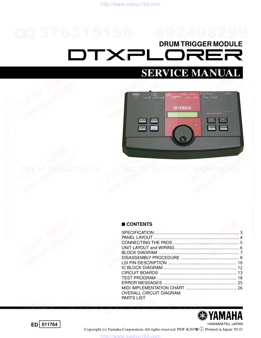
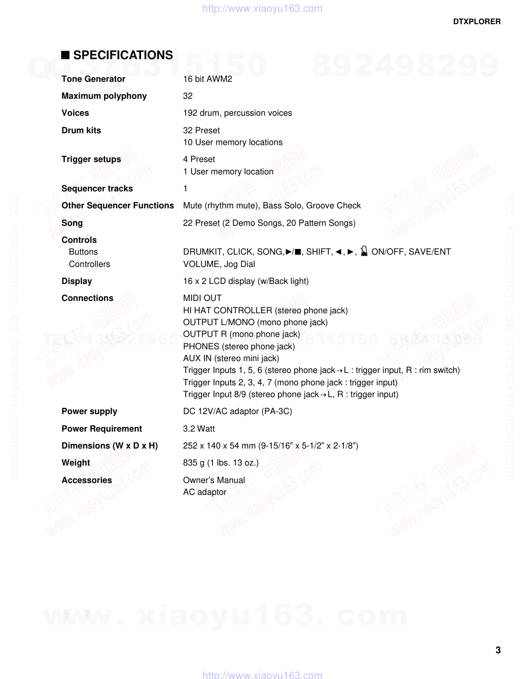
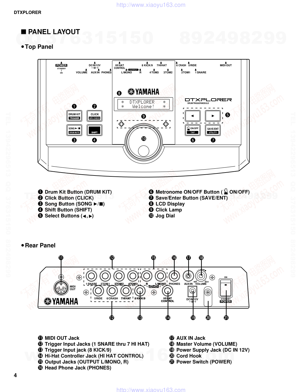
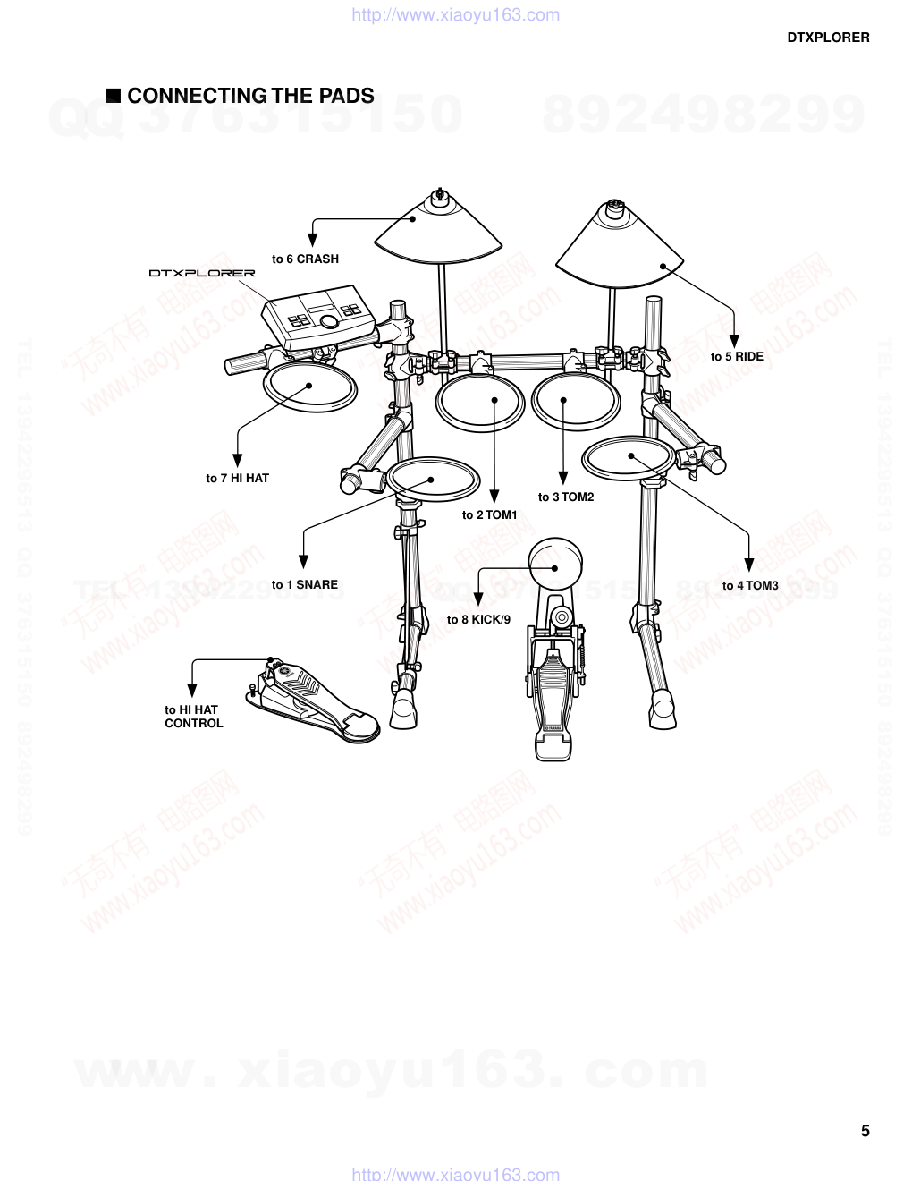
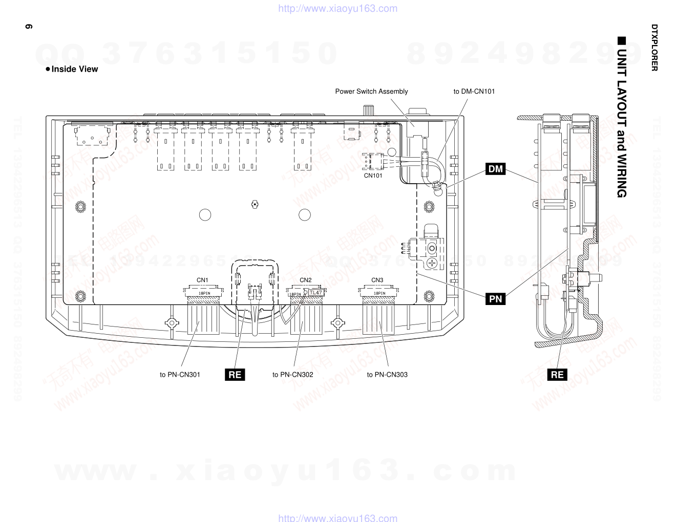
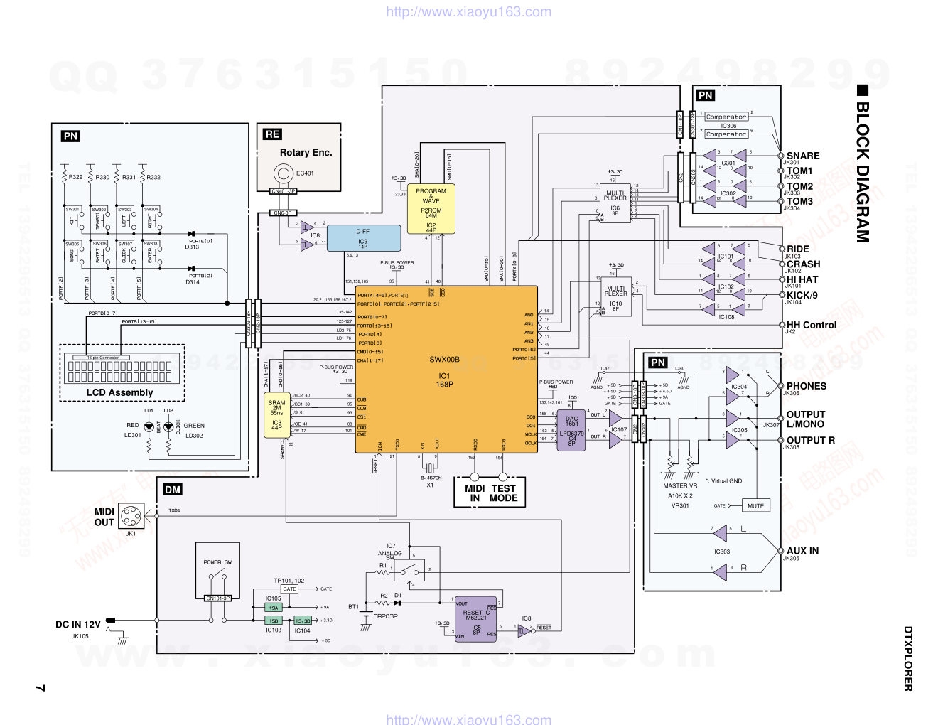
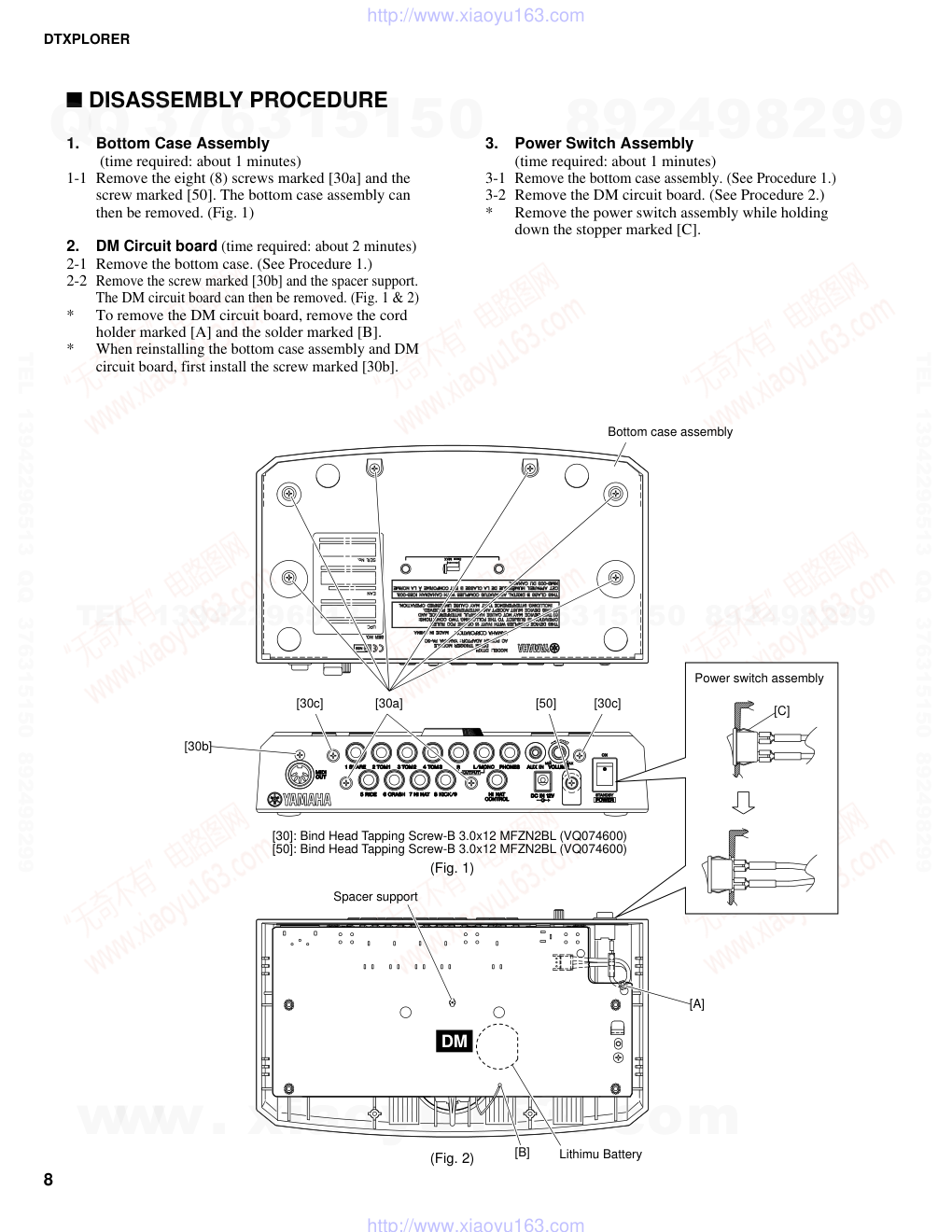
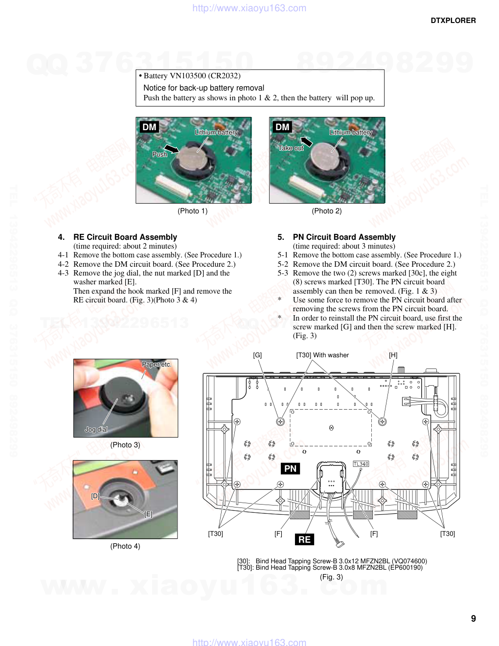
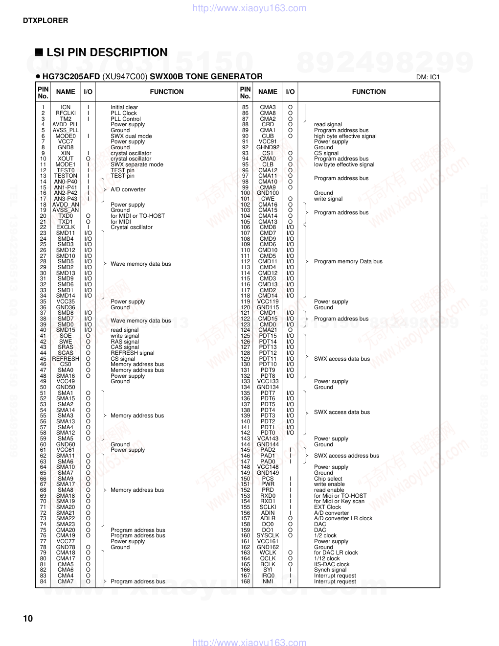
SERVICE MANUAL ED 011764 Copyright (c) Yamaha Corporation. All rights reserved. PDF-K265 IM Printed in Japan '05.01 I CONTENTS SPECIFICATION ....................................................................... 3 PANEL LAYOUT ........................................................................ 4 CONNECTING THE PADS........................................................ 5 UNIT LAYOUT and WIRING ...................................................... 6 BLOCK DIAGRAM .................................................................... 7 DISASSEMBLY PROCEDURE ................................................. 8 LSI PIN DESCRIPTION .......................................................... 10 IC BLOCK DIAGRAM.............................................................. 12 CIRCUIT BOARDS ................................................................. 13 TEST PROGRAM ................................................................... 18 ERROR MESSAGES .............................................................. 25 MIDI IMPLEMENTATION CHART ........................................... 26 OVERALL CIRCUIT DIAGRAM PARTS LIST DRUM TRIGGER MODULE www. xiaoyu163. com QQ 376315150 9 9 2 8 9 4 2 9 8 TEL 13942296513 9 9 2 8 9 4 2 9 8 0 5 1 5 1 3 6 7 3 Q Q TEL 13942296513 QQ 376315150 892498299 TEL 13942296513 QQ 376315150 892498299 http://www.xiaoyu163.com DTXPLORER 2 IMPORTANT NOTICE This manual has been provided for the use of authorized Yamaha Retailers and their service personnel. It has been assumed that basic service procedures inherent to the industry, and more specifically Yamaha Products, are already known and understood by the users, and have therefore not been restated. WARNING: Failure to follow appropriate service and safety procedures when servicing this product may result in personal injury, destruction of expensive components, and failure of the product to perform as specified. For these reasons, we advise all Yamaha product owners that all service required should be performed by an authorized Yamaha Retailer or the appointed service representative. IMPORTANT: The presentation or sale of this manual to any individual or firm does not constitute authorization, certification or recognition of any applicable technical capabilities, or establish a principle-agent relationship of any form. The data provided is believed to be accurate and applicable to the unit(s) indicated on the cover. The research, engineering, and service departments of Yamaha are continually striving to improve Yamaha products. Modifications are, therefore, inevitable and changes in specification are subject to change without notice or obligation to retrofit. Should any discrepancy appear to exist, please contact the distributor's Service Division. WARNING: Static discharges can destroy expensive components. Discharge any static electricity your body may have accumulated by grounding yourself to the ground bus in the unit (heavy gauge black wires connect to this bus). IMPORTANT: Turn the unit OFF during disassembly and part replacement. Recheck all work before you apply power to the unit. WARNING: CHEMICAL CONTENT NOTICE! The solder used in the production of this product contains LEAD. In addition, other electrical/electronic and /or plastic (where applicable) components may also contain traces of chemicals found by the California Health and Welfare Agency (and possibly other entities) to cause cancer and/or birth defects or other reproductive harm. DO NOT PLACE SOLDER, ELECTRICAL/ELECTRONIC OR PLASTIC COMPONENTS IN YOUR MOUTH FOR ANY REASON WHAT- SOEVER! Avoid prolonged, unprotected contact between solder and your skin! When soldering, do not inhale solder fumes or expose eyes to solder/flux vapor! If you come in contact with solder or components located inside the enclosure of this product, wash your hands before handling food. LITHIUM BATTERY HANDLING This product uses a lithium battery for memory back-up. WARNING: Lithium batteries are dangerous because they can be exploded by improper handling. Observe the following precautions when handling or replacing lithium batteries. • Leave lithium battery replacement to qualified service personnel. • Always replace with batteries of the same type. • When installing on the PC board by soldering, solder using the connection terminals provided on the battery cells. Never solder directly to the cells. Perform the soldering as quickly as possible. • Never reverse the battery polarities when installing. • Do not short the batteries. • Do not attempt to recharge these batteries. • Do not disassemble the batteries. • Never heat batteries or throw them into fire. ADVARSEL! Lithiumbatteri-Eksplosionsfare ved fejlagtig håndtering. Udskiftning må kun ske med batteri af samme fabrikat og type. Levér det brugte batteri tilbage til leverandoren. VARNING Explosionsfara vid felaktigt batteribyte. Använd samma batterityp eller en ekvivalent typ som rekommenderas av apparattillverkaren. Kassera använt batteri enligt fabrikantens instruktion. VAROITUS Paristo voi räjähtää, jos se on virheellisesti asennettu. Vaihda paristo ainoastaan laitevalmistajan suosittelemaan tyyppiin. Hävitä käytetty paristo valmistajan ohjeiden mukaisesti. The following information complies with Dutch Official Gazette 1995. 45; ESSENTIALS OF ORDER ON THE COLLECTION OF BATTERIES. • Please refer to the diassembly procedure for the removal of Back-up Battery. • Leest u voor het verwijderen van de backup batterij deze beschrijving. I WARNING Components having special characteristics are marked and must be replaced with parts having specification equal to those originally installed. www. xiaoyu163. com QQ 376315150 9 9 2 8 9 4 2 9 8 TEL 13942296513 9 9 2 8 9 4 2 9 8 0 5 1 5 1 3 6 7 3 Q Q TEL 13942296513 QQ 376315150 892498299 TEL 13942296513 QQ 376315150 892498299 http://www.xiaoyu163.com 3 DTXPLORER I SPECIFICATIONS Tone Generator 16 bit AWM2 Maximum polyphony 32 Voices 192 drum, percussion voices Drum kits 32 Preset 10 User memory locations Trigger setups 4 Preset 1 User memory location Sequencer tracks 1 Other Sequencer Functions Mute (rhythm mute), Bass Solo, Groove Check Song 22 Preset (2 Demo Songs, 20 Pattern Songs) Controls Buttons DRUMKIT, CLICK, SONG, / , SHIFT, , , ON/OFF, SAVE/ENT Controllers VOLUME, Jog Dial Display 16 x 2 LCD display (w/Back light) Connections MIDI OUT HI HAT CONTROLLER (stereo phone jack) OUTPUT L/MONO (mono phone jack) OUTPUT R (mono phone jack) PHONES (stereo phone jack) AUX IN (stereo mini jack) Trigger Inputs 1, 5, 6 (stereo phone jack→L : trigger input, R : rim switch) Trigger Inputs 2, 3, 4, 7 (mono phone jack : trigger input) Trigger Input 8/9 (stereo phone jack→L, R : trigger input) Power supply DC 12V/AC adaptor (PA-3C) Power Requirement 3.2 Watt Dimensions (W x D x H) 252 x 140 x 54 mm (9-15/16” x 5-1/2” x 2-1/8”) Weight 835 g (1 lbs. 13 oz.) Accessories Owner’s Manual AC adaptor www. xiaoyu163. com QQ 376315150 9 9 2 8 9 4 2 9 8 TEL 13942296513 9 9 2 8 9 4 2 9 8 0 5 1 5 1 3 6 7 3 Q Q TEL 13942296513 QQ 376315150 892498299 TEL 13942296513 QQ 376315150 892498299 http://www.xiaoyu163.com DTXPLORER 4 I PANEL LAYOUT q w e r t Drum Kit Button (DRUM KIT) Click Button (CLICK) Song Button (SONG / ) Shift Button (SHIFT) Select Buttons ( , ) y u i o !0 Metronome ON/OFF Button ( ON/OFF) Save/Enter Button (SAVE/ENT) LCD Display Click Lamp Jog Dial SAVE/ENT ON/OFF UTILITY TAP CLICK CLICK GRV.CHECK DRUM KIT TRIGGER TRIGGER SONG SONG DRUM MUTE / BEAT CLICK 1 SNARE 2 TOM1 3 TOM2 4 TOM3 DC IN 12V 5 RIDE PHONES 6 CRASH 7 HI HAT 8 KICK/9 L/MONO R MIDI OUT HI HAT CONTROL AUX IN VOLUME STANDBY ON DRUM TRIGGER MODULE SHIFT SHIFT * DTXPLORER * * Welcome! * q o !0 i w e r y u t 1 SNARE 1 SNARE 2 TOM1 2 TOM1 3 TOM2 3 TOM2 4 TOM3 4 TOM3 DC IN 12V DC IN 12V 5 RIDE 5 RIDE PHONES PHONES 6 CRASH 6 CRASH 7 HI HAT 7 HI HAT 8 KICK/9 8 KICK/9 MIDI OUT MIDI OUT HI HAT CONTROL HI HAT CONTROL AUX IN AUX IN VOLUME VOLUME STANDBY ON L/MONO L/MONO R MIN MAX !1 !2 !3 !4 !5 !6 !7 !8 !9 @0 @1 MIDI OUT Jack Trigger Input Jacks (1 SNARE thru 7 HI HAT) Trigger Input jack (8 KICK/9) Hi-Hat Controller Jack (HI HAT CONTROL) Output Jacks (OUTPUT L/MONO, R) Head Phone Jack (PHONES) AUX IN Jack Master Volume (VOLUME) Power Supply Jack (DC IN 12V) Cord Hook Power Switch (POWER) !1 !2 !5 !2 !4 !3 !6 !7 !8 !9 @0 @1 G Top Panel G Rear Panel www. xiaoyu163. com QQ 376315150 9 9 2 8 9 4 2 9 8 TEL 13942296513 9 9 2 8 9 4 2 9 8 0 5 1 5 1 3 6 7 3 Q Q TEL 13942296513 QQ 376315150 892498299 TEL 13942296513 QQ 376315150 892498299 http://www.xiaoyu163.com 5 DTXPLORER I CONNECTING THE PADS to 8 KICK/9 to 1 SNARE to 2 TOM1 to 3 TOM2 to 4 TOM3 to 5 RIDE to 6 CRASH to 7 HI HAT to HI HAT CONTROL www. xiaoyu163. com QQ 376315150 9 9 2 8 9 4 2 9 8 TEL 13942296513 9 9 2 8 9 4 2 9 8 0 5 1 5 1 3 6 7 3 Q Q TEL 13942296513 QQ 376315150 892498299 TEL 13942296513 QQ 376315150 892498299 http://www.xiaoyu163.com DTXPLORER 6 I UNIT LAYOUT and WIRING Inside View to PN-CN303 to DM-CN101 Power Switch Assembly to PN-CN302 to PN-CN301 CN3 CN101 CN2 CN1 PN DM RE RE www . x ia o y u 1 6 3 . c o m QQ 3 7 6 3 1 5 1 5 0 9 9 2 8 9 4 2 9 8 T E L 1 3 9 4 2 2 9 6 5 1 3 9 9 2 8 9 4 2 9 8 0 5 1 5 1 3 6 7 3 Q Q TEL 13942296513 QQ 376315150 892498299 TEL 13942296513 QQ 376315150 892498299 http://www.xiaoyu163.com 7 DTXPLORER I BLOCK DIAGRAM RE Rotary Enc. CN401-3P PROGRAM & WAVE P2ROM 64M IC2 44P 23,33 12 14 35 SWX00B IC1 168P SRAM 2M 55ns IC3 44P 8 9 XIN XOUT X1 /BC2 40 /BC1 39 /S 6 /OE 41 /W 17 90 95 93 88 101 119 1 21 135-142 125-127 LD2 75 LD1 76 133,143,161 DAC 16bit LPD6379 IC4 8P 8 158 6 + 5D TL47 TL340 AGND AGND + 4.5D + 9D GATE + 5D + 4.5D + 9A GATE 163 5 164 7 IC107 4 2 1 6 1 7 D-FF IC9 14P IC8 3 4 2 5 6 11 5,9,13 151,152,165 20,21,155,156,167,2 41 46 14 15 16 17 45 44 P-BUS POWER P-BUS POWER P-BUS POWER CN6-3P MULTI PLEXER IC10 8P MULTI PLEXER IC6 8P 12 14 15 11 1 5 2 4 13 3 10 9 13 10 9 12 14 16 16 IC301 IC302 IC101 IC102 IC108 JK301 JK302 JK303 JK304 JK103 JK102 JK101 JK104 JK2 JK306 JK307 JK308 JK305 IC306 1 2 7 6 CN1-18P CN301-18P PN PN PN DM 1 3 7 5 14 12 8 10 1 3 7 5 14 12 8 10 1 3 7 5 14 12 8 10 1 3 7 5 14 12 8 10 7 5 1 3 CN302 CN2 CN303-18P CN3-18P MASTER VR A10K X 2 VR301 IC304 IC305 3 1 5 7 3 1 5 7 7 5 1 3 IC303 *: Virtual GND * * CN302 CN2 IC8 1 2 5 1 7 3 RESET IC M62021 IC5 8P IC7 1 2 IC105 TR101, 102 IC103 IC104 JK105 JK1 CN101-3P RED LD301 GREEN LD302 D313 D314 SW301 SW302 SW303 SW304 SW305 SW306 SW307 SW308 CN2-18P CN302-18P CN2-18P EC401 ,PORTE[7] 154 153 33 5 4 D1 MUTE R1 R2 BT1 R329 R330 R331 R332 DC IN 12V PHONES RIDE SNARE TOM1 TOM2 TOM3 CRASH HI HAT KICK/9 HH Control AUX IN OUTPUT L/MONO OUTPUT R MIDI OUT MIDI IN TEST MODE LCD Assembly 16 pin Connector + 3.3D + 5D GATE + 9A GATE GATE www . x ia o y u 1 6 3 . c o m QQ 3 7 6 3 1 5 1 5 0 9 9 2 8 9 4 2 9 8 T E L 1 3 9 4 2 2 9 6 5 1 3 9 9 2 8 9 4 2 9 8 0 5 1 5 1 3 6 7 3 Q Q TEL 13942296513 QQ 376315150 892498299 TEL 13942296513 QQ 376315150 892498299 http://www.xiaoyu163.com DTXPLORER 8 I DISASSEMBLY PROCEDURE 1. Bottom Case Assembly (time required: about 1 minutes) 1-1 Remove the eight (8) screws marked [30a] and the screw marked [50]. The bottom case assembly can then be removed. (Fig. 1) 2. DM Circuit board (time required: about 2 minutes) 2-1 Remove the bottom case. (See Procedure 1.) 2-2 Remove the screw marked [30b] and the spacer support. The DM circuit board can then be removed. (Fig. 1 & 2) * To remove the DM circuit board, remove the cord holder marked [A] and the solder marked [B]. * When reinstalling the bottom case assembly and DM circuit board, first install the screw marked [30b]. (Fig. 2) [30]: Bind Head Tapping Screw-B 3.0x12 MFZN2BL (VQ074600) [50]: Bind Head Tapping Screw-B 3.0x12 MFZN2BL (VQ074600) (Fig. 1) 3. Power Switch Assembly (time required: about 1 minutes) 3-1 Remove the bottom case assembly. (See Procedure 1.) 3-2 Remove the DM circuit board. (See Procedure 2.) * Remove the power switch assembly while holding down the stopper marked [C]. Bottom case assembly Lithimu Battery [30a] [30c] [30b] Spacer support [50] [30c] DM [C] Power switch assembly [A] [B] www. xiaoyu163. com QQ 376315150 9 9 2 8 9 4 2 9 8 TEL 13942296513 9 9 2 8 9 4 2 9 8 0 5 1 5 1 3 6 7 3 Q Q TEL 13942296513 QQ 376315150 892498299 TEL 13942296513 QQ 376315150 892498299 http://www.xiaoyu163.com 9 DTXPLORER 4. RE Circuit Board Assembly (time required: about 2 minutes) 4-1 Remove the bottom case assembly. (See Procedure 1.) 4-2 Remove the DM circuit board. (See Procedure 2.) 4-3 Remove the jog dial, the nut marked [D] and the washer marked [E]. Then expand the hook marked [F] and remove the RE circuit board. (Fig. 3)(Photo 3 & 4) [30]: Bind Head Tapping Screw-B 3.0x12 MFZN2BL (VQ074600) [T30]: Bind Head Tapping Screw-B 3.0x8 MFZN2BL (EP600190) (Fig. 3) (Photo 4) (Photo 3) (Photo 2) (Photo 1) 5. PN Circuit Board Assembly (time required: about 3 minutes) 5-1 Remove the bottom case assembly. (See Procedure 1.) 5-2 Remove the DM circuit board. (See Procedure 2.) 5-3 Remove the two (2) screws marked [30c], the eight (8) screws marked [T30]. The PN circuit board assembly can then be removed. (Fig. 1 & 3) * Use some force to remove the PN circuit board after removing the screws from the PN circuit board. * In order to reinstall the PN circuit board, use first the screw marked [G] and then the screw marked [H]. (Fig. 3) [T30] [G] [H] With washer [T30] [T30] Battery VN103500 (CR2032) Notice for back-up battery removal Push the battery as shows in photo 1 & 2, then the battery will pop up. RE PN [D] [D] [E] [E] Jog dial Jog dial DM DM Lithium battery Lithium battery Lithium battery Lithium battery Push Push Take out Take out [F] [F] Paper etc. Paper etc. www. xiaoyu163. com QQ 376315150 9 9 2 8 9 4 2 9 8 TEL 13942296513 9 9 2 8 9 4 2 9 8 0 5 1 5 1 3 6 7 3 Q Q TEL 13942296513 QQ 376315150 892498299 TEL 13942296513 QQ 376315150 892498299 http://www.xiaoyu163.com DTXPLORER 10 I LSI PIN DESCRIPTION PIN No. NAME I/O FUNCTION PIN No. NAME I/O FUNCTION 1 2 3 4 5 6 7 8 9 10 11 12 13 14 15 16 17 18 19 20 21 22 23 24 25 26 27 28 29 30 31 32 33 34 35 36 37 38 39 40 41 42 43 44 45 46 47 48 49 50 51 52 53 54 55 56 57 58 59 60 61 62 63 64 65 66 67 68 69 70 71 72 73 74 75 76 77 78 79 80 81 82 83 84 ICN RFCLKI TM2 AVDD_PLL AVSS_PLL MODE0 VCC7 GND8 XIN XOUT MODE1 TEST0 TESTON AN0-P40 AN1-P41 AN2-P42 AN3-P43 AVDD_AN AVSS_AN TXD0 TXD1 EXCLK SMD11 SMD4 SMD3 SMD12 SMD10 SMD5 SMD2 SMD13 SMD9 SMD6 SMD1 SMD14 VCC35 GND36 SMD8 SMD7 SMD0 SMD15 SOE SWE SRAS SCAS REFRESH CS0 SMA0 SMA16 VCC49 GND50 SMA1 SMA15 SMA2 SMA14 SMA3 SMA13 SMA4 SMA12 SMA5 GND60 VCC61 SMA11 SMA6 SMA10 SMA7 SMA9 SMA17 SMA8 SMA18 SMA19 SMA20 SMA21 SMA22 SMA23 CMA20 CMA19 VCC77 GND78 CMA18 CMA17 CMA5 CMA6 CMA4 CMA7 I I I I I O I I I I I I I O O I I/O I/O I/O I/O I/O I/O I/O I/O I/O I/O I/O I/O I/O I/O I/O I/O O O O O O O O O O O O O O O O O O O O O O O O O O O O O O O O O O O O O O O O Initial clear PLL Clock PLL Control Power supply Ground SWX dual mode Power supply Ground crystal oscillator crystal oscillator SWX separate mode TEST pin TEST pin A/D converter Power supply Ground for MIDI or TO-HOST for MIDI Crystal oscillator Wave memory data bus Power supply Ground Wave memory data bus read signal write signal RAS signal CAS signal REFRESH signal CS signal Memory address bus Memory address bus Power supply Ground Memory address bus Ground Power supply Memory address bus Program address bus Program address bus Power supply Ground Program address bus 85 86 87 88 89 90 91 92 93 94 95 96 97 98 99 100 101 102 103 104 105 106 107 108 109 110 111 112 113 114 115 116 117 118 119 120 121 122 123 124 125 126 127 128 129 130 131 132 133 134 135 136 137 138 139 140 141 142 143 144 145 146 147 148 149 150 151 152 153 154 155 156 157 158 159 160 161 162 163 164 165 166 167 168 CMA3 CMA8 CMA2 CRD CMA1 CUB VCC91 GHND92 CS1 CMA0 CLB CMA12 CMA11 CMA10 CMA9 GND100 CWE CMA16 CMA15 CMA14 CMA13 CMD8 CMD7 CMD9 CMD6 CMD10 CMD5 CMD11 CMD4 CMD12 CMD3 CMD13 CMD2 CMD14 VCC119 GND115 CMD1 CMD15 CMD0 CMA21 PDT15 PDT14 PDT13 PDT12 PDT11 PDT10 PDT9 PDT8 VCC133 GND134 PDT7 PDT6 PDT5 PDT4 PDT3 PDT2 PDT1 PDT0 VCA143 GND144 PAD2 PAD1 PAD0 VCC148 GND149 PCS PWR PRD RXD0 RXD1 SCLKI ADIN ADLR DO0 DO1 SYSCLK VCC161 GND162 WCLK QCLK BCLK SYI IRQ0 NMI O O O O O O O O O O O O O O O O O O I/O I/O I/O I/O I/O I/O I/O I/O I/O I/O I/O I/O I/O I/O I/O I/O O I/O I/O I/O I/O I/O I/O I/O I/O I/O I/O I/O I/O I/O I/O I/O I/O I I I I I I I I I I O O O O O O O I I I read signal Program address bus high byte effective signal Power supply Ground CS signal Program address bus low byte effective signal Program address bus Ground write signal Program address bus Program memory Data bus Power supply Ground Program address bus SWX access data bus Power supply Ground SWX access data bus Power supply Ground SWX access address bus Power supply Ground Chip select write enable read enable for Midi or TO-HOST for Midi or Key scan EXT Clock A/D converter A/D converter LR clock DAC DAC 1/2 clock Power supply Ground for DAC LR clock 1/12 clock IIS-DAC clock Synch signal Interrupt request Interrupt request G HG73C205AFD (XU947C00) SWX00B TONE GENERATOR DM: IC1 www. xiaoyu163. com QQ 376315150 9 9 2 8 9 4 2 9 8 TEL 13942296513 9 9 2 8 9 4 2 9 8 0 5 1 5 1 3 6 7 3 Q Q TEL 13942296513 QQ 376315150 892498299 TEL 13942296513 QQ 376315150 892498299 http://www.xiaoyu163.com 11 DTXPLORER PIN No. NAME I/O FUNCTION PIN No. NAME I/O FUNCTION 1 2 3 4 ROUT REF Vss LOUT O O Rch analog output Voltage reference Ground Lch analog output 5 6 7 8 LRCK SI CLK Vdd I I I L/R Clock Sirial data input Shift clock Power supply +5A UPD6379A (XR998A00) DAC (Digital to Analog Converter) DM: IC4 www. xiaoyu163. com QQ 376315150 9 9 2 8 9 4 2 9 8 TEL 13942296513 9 9 2 8 9 4 2 9 8 0 5 1 5 1 3 6 7 3 Q Q TEL 13942296513 QQ 376315150 892498299 TEL 13942296513 QQ 376315150 892498299 http://www.xiaoyu163.com DTXPLORER 12 I IC BLOCK DIAGRAM G NJM2903M-TE1 (X5814A00) G NJM2904M (XV190A00) G NJM4556AM-TE1 (X5049A00) G UPC4570GG2 (XF291A00) Dual Operational Amplifier DM: IC106, 107, 108 PN: IC303, 304, 305, 306 G TC7S66FU (XR867A00) Analog Switch DM: IC7 G TC74HC4052AFT (XV869A00) Differential 4-Channel Multiplexer/Demultiplexer DM: IC6, 10 G TC7S32F (XM588A00) OR DM: IC12 D OUTPUT D -INPUT C OUTPUT B -INPUT A OUTPUT 1 2 3 4 5 6 7 8 9 10 11 12 13 14 C +INPUT B +INPUT A +INPUT A -INPUT D +INPUT C -INPUT B OUTPUT NJM2902M-TE1 (X4983A00) Quad Operational Amplifier DM: IC101, 102 PN: IC301, 302 74HC74DT (X2171A00) Dual D-Type Flip-Flop DM: IC9 + - + - + - + - -V +V Vcc OUT 1 2 3 5 4 IN A IN B Vss Vcc COUT 1 2 3 5 4 IN / OUT OUT / IN GND G SN74HC14PWR (XZ288A00) Hex Inverter DM: IC8 1 1A 2 3 4 5 6 7 1Y 2A 2Y 3A 3Y GND 8 9 10 11 12 13 14 VDD 6A 6Y 5A 5Y 4A 4Y Vcc 2CLR 2Q GND 1Q 1PR 1CRL 1 2 3 4 5 6 7 8 9 10 11 12 13 14 2PR 1Q 1CK 1D 2D 2CK 2Q Q PR Q CK D Q PR D CK Q CLR CLR INPUTS OUTPUTS L L H H H H PR H L L H H H CLR X X X L CLK X X X H L X D H H L H L Q Q L H H L H Q Q 1 2 3 4 5 6 7 0Y 2Y Y-COM 1Y INH VEE VSS 3Y 16 15 14 13 12 11 VDD 2X 1X X-COM 0X 3X A 8 9 10 B 2Y 0Y Y-COM 3Y 1Y INH B 2X 1X X-COM 0X 3X A 1 2 3 4 8 7 6 5 Output A Non-Inverting Input A -DC Voltage Supply (GND) +DC Voltage Supply Output B Inverting Input B Non-Inverting Input B Inverting Input A + - + - A B VOUT VBAT CS Ct RES VIN RES SW Reset Delay D1 R2 1.24V R1 RES GND 1 2 3 4 5 6 7 8 CS VIN Ct VOUT VBAT GND RES M62023FP (X2163A00) System Reset DM: IC5 + - 3 7 5 6 8 4 2 1 www. xiaoyu163. com QQ 376315150 9 9 2 8 9 4 2 9 8 TEL 13942296513 9 9 2 8 9 4 2 9 8 0 5 1 5 1 3 6 7 3 Q Q TEL 13942296513 QQ 376315150 892498299 TEL 13942296513 QQ 376315150 892498299 http://www.xiaoyu163.com 13 DTXPLORER I CIRCUIT BOARDS to PN-CN301 to PN-CN302 to PN-CN303 to Power Switch MIDI OUT 5.RIDE 6.CRASH 7.HI HAT 8.KICK/9 Rotary encoder H.H.CONT DC IN 12V DM Circuit Board (Version C) RE Circuit Board (Same as for version D) Component side Component side DM, RE: ENA-WD41150 0 1. Add a resister (V973290: RES CARBON FILM 1.0K 1/8W) between R16 and a through hole of DGND referring to pic.1&2. Confirm that one leg of the resister pierce to the through hole. 2. Check the value of resistance between the point indicated by arrow and DGND. Confirm the value is about 1.1k ohm. (Refer to pic.2) www . x ia o y u 1 6 3 . c o m QQ 3 7 6 3 1 5 1 5 0 9 9 2 8 9 4 2 9 8 T E L 1 3 9 4 2 2 9 6 5 1 3 9 9 2 8 9 4 2 9 8 0 5 1 5 1 3 6 7 3 Q Q TEL 13942296513 QQ 376315150 892498299 TEL 13942296513 QQ 376315150 892498299 http://www.xiaoyu163.com DTXPLORER 14 DM Circuit Board (Version C) Pattern side Pattern side RE Circuit Board (Same as for version D) www . x ia o y u 1 6 3 . c o m QQ 3 7 6 3 1 5 1 5 0 9 9 2 8 9 4 2 9 8 T E L 1 3 9 4 2 2 9 6 5 1 3 9 9 2 8 9 4 2 9 8 0 5 1 5 1 3 6 7 3 Q Q TEL 13942296513 QQ 376315150 892498299 TEL 13942296513 QQ 376315150 892498299 http://www.xiaoyu163.com 15 DTXPLORER to PN-CN301 to PN-CN302 to PN-CN303 to Power Switch MIDI OUT 5.RIDE 6.CRASH 7.HI HAT 8.KICK/9 H.H.CONT DC IN 12V DM Circuit Board (Version D) Component side DM, RE: ENA-WD41150 0 Rotary encoder RE Circuit Board (Same as for version C) Component side www . x ia o y u 1 6 3 . c o m QQ 3 7 6 3 1 5 1 5 0 9 9 2 8 9 4 2 9 8 T E L 1 3 9 4 2 2 9 6 5 1 3 9 9 2 8 9 4 2 9 8 0 5 1 5 1 3 6 7 3 Q Q TEL 13942296513 QQ 376315150 892498299 TEL 13942296513 QQ 376315150 892498299 http://www.xiaoyu163.com DTXPLORER 16 DM Circuit Board (Version D) Pattern side Pattern side RE Circuit Board (Same as for version C) www . x ia o y u 1 6 3 . c o m QQ 3 7 6 3 1 5 1 5 0 9 9 2 8 9 4 2 9 8 T E L 1 3 9 4 2 2 9 6 5 1 3 9 9 2 8 9 4 2 9 8 0 5 1 5 1 3 6 7 3 Q Q TEL 13942296513 QQ 376315150 892498299 TEL 13942296513 QQ 376315150 892498299 http://www.xiaoyu163.com 17 DTXPLORER Pattern side L/MONO -OUTPUT- R 4 TOM3 3 TOM2 2 TOM1 1 SNARE PHONES AUX IN VOL PN Circuit Board (Same as for version C) Component side DM, RE: ENA-WD41150 0 to DM-CN1 to DM-CN2 to DM-CN3 www. xiaoyu163. com QQ 376315150 9 9 2 8 9 4 2 9 8 TEL 13942296513 9 9 2 8 9 4 2 9 8 0 5 1 5 1 3 6 7 3 Q Q TEL 13942296513 QQ 376315150 892498299 TEL 13942296513 QQ 376315150 892498299 http://www.xiaoyu163.com DTXPLORER 18 I TEST PROGRAM A B C C-01. C-02. C-03. C-04. C-05. C-06. C-07. C-08. C-09. C-10. C-11. C-12. C-13. C-14. C-15. C-16. C-17. C-18. C-19. C-20. C-21. C-22. C-23. C-24. C-25. C-26. C-27. MEASURING CONDITION TEST ENTRY CARRYING ON THE TEST AND THE TEST AT THE TIME OF FAIL TEST ITEM ROM SRAM BATTERY MIDI OUT LCD LED SW ROTARY ENCODER TRIGGER IN 1 PROGRAM ROM READ (Automatic test) SRAM READ / WRITE (Automatic test) BUTTON BATTERY (Automatic test) OUTPUT AT KEY ON/OFF CHECK VISUALLY / DISPLAY EACH PATTERN ON LCD CHECK VISUALLY / LED ON/OFF PANEL SWITCH ON LEFT, RIGHT TRIGGER IN 2 TRIGGER IN 3 TRIGGER IN 4 TRIGGER IN 5 TRIGGER IN 6 TRIGGER IN 7 TRIGGER IN 8 RIM SW L IN 1 TRIGGER IN 9 RIM SW IN 1 RIM SW IN 5 RIM SW IN 6 HI HAT CONTROL OUTPUT L 1 kHz OUTPUT R 1 kHz AUX IN 32 ch OUT FACTORY SET Check the switch for ON/OFF operation. (3 zone side) Check the switch for ON/OFF operation. Check the switch for ON/OFF operation. Check the switch for ON/OFF operation. Maximum, Minimum Measurement Measurement Measurement Auditory check Test No. Title Judgment criteria, etc. L R R L Measuring condition 1) Use PA-3C (adapter). 2) Measuring instrunments Low-frequency oscillator, level meter, analog waveform measuring instrument, and powered speaker. * To measure audio output, use JIS C filter. 3) Jigs MIDI cable, USB cable, stereo (TRS) phone cable, and MIDI IN compatible module. Pad with 3 zone RIM switch (TP-65S etc.), HI-HAT controller. (HH65) Stereo phone cable www. xiaoyu163. com QQ 376315150 9 9 2 8 9 4 2 9 8 TEL 13942296513 9 9 2 8 9 4 2 9 8 0 5 1 5 1 3 6 7 3 Q Q TEL 13942296513 QQ 376315150 892498299 TEL 13942296513 QQ 376315150 892498299 http://www.xiaoyu163.com 19 DTXPLORER A. TEST ENTRY Perform the following operation when turning on power for the main unit. Turn on power for the main unit while holding down the following buttons at the same time. [KIT]+[SAVE/ENTER] In case of any change, set each of the parameters below. *Note that the change from ver. 1.00 to 1.02 is followed by a change of CR value. Also change ver. 1.00 to "3a50" and check it. For parameter setting, select the parameter you want to change using [←] and [→], and set it with ROTARY ENCODER. Each parameter is detailed below. All parameters are ranged from 00 to ff. The values referred to as the upper and lower limits are also included in the OK range. 67 Lower limit in the OK range in INPUT 1-9 7f Upper limit in the OK range in INPUT 1-9 3a Lower limit in the OK range after elapse of time in the time constant test for INPUT 1-9 50 Upper limit in the OK range after elapse of time in the time constant test for INPUT 1-9 04 Upper limit for the cross talk value in INPUT 1-9 *After changing all parameters, press [SAVE/ENTER] and the "Test No. Selection Screen" appears. B. CARRYING ON THE TEST AND THE TEST AT THE TIME OF FAIL In case of TEST ENTRY, the following screen first appears. In case of any chang, set each parameter below. For parameter setting, select the parmeter you want to change using [←] and [→], and set it with ROTARY ENCODER. Pressing the [SAVE/ENTER] key displays the following screen. This state is called the "Test No. Selection Screen". Using the [←] and [→] keys, select the Test No. and press the [SAVE/ENTER] key. The test can be automatically performed in order of Test No. starting with the selected Test No. In case of failure, the test stops with FAIL indicated. Carrying on the test which is judged to be FAIL. Press the [SHIFT] key in case each test is judged to be FAIL. The Test No. Selection Screen will appear. DIAG att cr xt 677f 3a50 04 DIAG att cr xt 677f 3a50 04 1 ROM C-01. ROM [Initial indication] [Test content] Read the data for ROM (IC2) and verify it. [Test method] Perform the test. [Check item] Check the result on the LCD. [Indication of judgment result] In case of OK Go on to the next test. In case of NG [Content of FAIL judgment] Not available [Completing the test] OK: The test will proceed to the next one automatically. NG: For handling the FAIL judgment, see "B. CARRYING ON THE TEST". C-2. SRAM [Initial indication] [Test content] WRITE/READ the data "A5" to SRAM (IC3) and perform Verify Check. [Test method] Perform the test. [Check item] Check the result on the LCD. [Indication of judgment result] In case of OK Go on to the next test. In case of NG [Content of FAIL judgment] Not available [Completing the test] OK: The test will proceed to the next one automatically. NG: For handling the FAIL judgment, see "B. CARRYING ON THE TEST". 1 ROM 1 ROM FAIL **** 2 SRAM 2 SRAM FAIL www. xiaoyu163. com QQ 376315150 9 9 2 8 9 4 2 9 8 TEL 13942296513 9 9 2 8 9 4 2 9 8 0 5 1 5 1 3 6 7 3 Q Q TEL 13942296513 QQ 376315150 892498299 TEL 13942296513 QQ 376315150 892498299 http://www.xiaoyu163.com DTXPLORER 20 [Completing the test] OK: In case of OK, press [SAVE/ENTER]. The test proceeds to the next one. NG: For handling the FAIL judgment, see "B. CARRYING ON THE TEST". C-05. LCD [Initial indication] [Test content] Visually check the dots on the LCD. [Test method] Check that all dots flash on and off alternately. [Check item] Check the result on the LCD. [Indication of judgment result] Not available [Content of FAIL judgment] Not available [Completing the test] OK: In case of OK, press [SAVE/ENTER]. The test proceeds to the next one. NG: For handling the FAIL judgment, see "B. CARRYING ON THE TEST". C-6. LED [Initial indication] [Test content] Make sure that the LED lights up correctly. [Test method] Check that the LEDs light up in the following order. BEAT (RED) → CLICK (GREEN) → Both light up. [Check item] Check that the LEDs light up in the above order. Visually check that the LEDs are not too dark. [Indication of judgment result] Not available [Content of FAIL judgment] Not available [Completing the test] OK: In case of OK, press [SAVE/ENTER]. The test proceeds to the next one. NG: For handling the FAIL judgment, see "B. CARRYING ON THE TEST". C-03. BATTERY [Initial indication] [Test content] Check that the battery is new. [Test method] Perform the test. [Check item] Check the result on the LCD. [Indication of judgment result] In case of OK Go on to the next test. In case of NG [Content of FAIL judgment] Not available [Completing the test] OK: The test will proceed to the next one automatically. NG: For handling the FAIL judgment, see "B. CARRYING ON THE TEST". C-4. MIDI OUT [Initial indication] [Test content] Output key on (90 3C 7F) from MIDI OUT. Output key off (90 3C 00) after 500 msec. [Test method] After connecting MIDI OUT and I/O box with the MIDI cable, perform the test. [Check item] Check that MIDI code is transmitted. [Indication of judgment result] Not available [Content of FAIL judgment] Not available 3 BATTERY 3 BATTERY FAIL 4 MIDI OUT 5 LCD 6 LED MIDI OUT MIDI cable MIDI IN DTXPLORER MIDI instrument www. xiaoyu163. com QQ 376315150 9 9 2 8 9 4 2 9 8 TEL 13942296513 9 9 2 8 9 4 2 9 8 0 5 1 5 1 3 6 7 3 Q Q TEL 13942296513 QQ 376315150 892498299 TEL 13942296513 QQ 376315150 892498299 http://www.xiaoyu163.com 21 DTXPLORER C-8. ROTARY ENCODER [Initial indication] [Test content] Make sure that ROTARY ENCODER operates correctly. [Test method] Rotate ROTARY ENCODER clockwise or anticlockwise according to the LCD indication. [Check item] Check the result on the LCD. [Indication of judgment result] In case of OK Go on to the next test. In case of NG [Content of FAIL judgment] Not available [Completing the test] OK: The test will proceed to the next one automatically. NG: For handling the FAIL judgment, see "B. CARRYING ON THE TEST". C-9. TRIGGER IN 1 C-10. TRIGGER IN 2 C-11. TRIGGER IN 3 C-12. TRIGGER IN 4 C-13. TRIGGER IN 5 C-14. TRIGGER IN 6 C-15. TRIGGER IN 7 C-16. TRIGGER IN 8 C-17. TRIGGER IN 9 [Initial indication] [Test content] Add looped signals from PHONES when inputting 1.SNARE — 8.KICK/9 and check that the inputted signals are entered into CPU with correct values. Also check that no signals are leaked to other inputs. *Output wave from PHONES is a tone burst sine wave with a frequency of 4 kHz and +4 dBm (load of 10 k ohm). C-07. PANEL SWITCH [Initial indication] [Test content] Make sure that the panel switches turn on and off correctly. [Test method] Turn on the panel switches from [KIT] to [SAVE/ENTER] according to the LCD indication as shown below. [ KIT ] [ CLICK ] [ SONG ] [ SHIFT ] [ <- ] [ -> ] [CLKPLAY] [ SAVE/ ] [Check item] Check the result on the LCD. [Indication of judgment result] In case of OK Go on to the next test. In case of NG [Content of FAIL judgment] Not available [Completing the test] OK: The test will proceed to the next one automatically. NG: For handling the FAIL judgment, see "B. CARRYING ON THE TEST". 7 SW FAIL 7 SW [ KIT ] SAVE/ENT ON/OFF UTILITY TAP CLICK CLICK GRV.CHECK DRUM KIT TRIGGER TRIGGER SONG SONG DRUM MUTE / SHIFT SHIFT 8 R.Encoder 8 R.Encoder CLOCKWIZE 8 R.Encoder ANTICLOCKWIZE 8 R.Encoder FAIL 9 TRIGGER IN01 waiting too Lo www. xiaoyu163. com QQ 376315150 9 9 2 8 9 4 2 9 8 TEL 13942296513 9 9 2 8 9 4 2 9 8 0 5 1 5 1 3 6 7 3 Q Q TEL 13942296513 QQ 376315150 892498299 TEL 13942296513 QQ 376315150 892498299 http://www.xiaoyu163.com DTXPLORER 22 The above appears, so press the switch for the 3 zone side. In case of OK, proceed to the next one and enter into 5.RIDE. Likewise, check up to 6.CRASH. [Check item] Check the result on the LCD. [Indication of judgment result] In case of OK Go on to the next test. In case of NG [Content of FAIL judgment] The test no longer proceeds to the next one. [Completing the test] OK: The test will proceed to the next one automatically. NG: For handling the FAIL judgment, see "B. CARRYING ON THE TEST". C-22. HI HAT CONTROL [Initial indication] [Test content] Check that the HI-HAT controller allows the control to operate correctly. [Test method] Insert the HI-HAT controller plug into the jack of HI-HAT control. Operate the sensor to the upper and the lower limit. (Order does not matter.) [Check item] Check the result on the LCD. [Indication of judgment result] In case of OK Go on to the next test. In case of NG Not available [Content of FAIL judgment] Controller operation will not allow the next test to follow. [Completing the test] OK: The test will proceed to the next one automatically. C-23. OUTPUT L 1 kHz [Initial indication] [Test content] Check that correct signals are outputted from OUTPUT (L/MONO). 29 RIM SW IN01 FAIL 22 H.H. CONT. [Test method] Maximize VOLUME. Put in the stero cable looped from PHONES in order starting with 1.SNARE. In case of OK, proceed to the next INPUT and the following apperas. So, put in 2.TOM1. Repeat the sequence until it gets to 8.KICK/9. [Check item] Check the result on the LCD. [Indication of judgment result] In case of OK Go on to the next test. In case of NG XXXXX refers to "too High", "XtalkIN2", "BAD CR", etc. [Content of FAIL judgment] The test no longer proceeds to the next one. [Completing the test] OK: The test will proceed to the next one automatically. NG: For handling the FAIL judgment, see "B. CARRYING ON THE TEST". C-18. RIM SW IN 1 C-19. RIM SW L IN 1 C-20. RIM SW IN 5 C-21. RIM SW IN 6 [Initial indication] [Test content] For input at three locations, i.e. 1.SNARE, 5.RIDE, and 6.CRASH, connect the RIM switch-fitted pad and check for correct operation. For IN1, also check 3 zone rim switch. [Test method] Connect the 3 zone RIM switch-fitted pad with each jack in order of INPUT 1, 5, and 6 and turn on the RIM switch. In case of OK 9 TRIGGER IN02 waiting too Lo 18 RIM SW IN01 waiting 19 RIM SW L IN01 waiting 9 TRIGGER IN02 FAIL XXXXX 18 RIM SW IN01 waiting 23 OUTPUT L 1kHz www. xiaoyu163. com QQ 376315150 9 9 2 8 9 4 2 9 8 TEL 13942296513 9 9 2 8 9 4 2 9 8 0 5 1 5 1 3 6 7 3 Q Q TEL 13942296513 QQ 376315150 892498299 TEL 13942296513 QQ 376315150 892498299 http://www.xiaoyu163.com 23 DTXPLORER [Indication of judgment result] Not available [Content of FAIL judgment] Not available [Completing the test] OK: In case of OK, press [SAVE/ENTER]. The test proceeds to the next one. NG: For handling the FAIL judgment, see "B. CARRYING ON THE TEST". C-25. AUX IN [Initial indication] [Test content] Check that the signals coming in form AUX IN are bieng outputted as correct signals. [Test method] Input sine waves into AUX IN (L, R) and with the standard stereo phone plugs inserted into PHONES (L, R), measure the frequency and output wave level of PHONES. [Check item] Input a sine wave of -20 dBm and 1 kHz into AUX IN (L) (with AUX IN (R) grounded). Maximize VOLUME. PHONES (L): -7.0 +/-2 dBm (Load of 33 ohm), distortion factor of 0.5 % or less*1 PHONES (R): -65 dBm or less*2 (Load of 33 ohm) Input a sine wave of -20 dBm and 1 kHz into AUX IN (R) (with AUX IN (L) grounded). Maximize VOLUME. PHONES (L): -65 dBm or less*2 (Load of 33 ohm) PHONES (R): -7.0 +/-2 dBm (Load of 33 ohm), distortion factor of 0.5 % or less*1 *1,*2: For inspection of the circuit board, the distortion factor must be 1.0 % or less and the sound -60 dBm or less. [Indication of judgment result] Not available [Content of FAIL judgment] Not available [Completing the test] OK: In case of OK, press [SAVE/ENTER]. The test proceeds to the next one. NG: For handling the FAIL judgment, see "B. CARRYING ON THE TEST". C-26. 32 ch OUT [Initial indication] 25 AUX INPUT [Test method] Insert the phone plugs into OUTPUT (for L/MONO, R) and measure the frequency, output waveform, and output level of each output. Maximize VOLUME. For AUX IN, make sure that the plug is not inserted or that the input voltage is -70 dBm or less. [Check item] OUTPUT (L/MONO): 1 kHz +/- 3 Hz, SIN wave, -5.5 +/-2 dBm (load of 10 k ohm), distortion factor of 0.5 % or less*1 OUTPUT (R): -65 dBm or less*2 (load of 10 k ohm) In case the plug is pulled out of OUTPUT (R) OUTPUT (L/MONO): 1 kHz +/- 3 Hz, SIN wave, -11.0 +/-2 dBm (load of 10 k ohm), distortion factor of 0.5 % or less*1 *1,*2: For inspection of the circuit board, the distortion factor must be 1.0 % or less and the sound -60 dBm or less. [Indication of judgment result] Not available [Content of FAIL judgment] Not available [Completing the test] OK: In case of OK, press [SAVE/ENTER]. The test proceeds to the next one. NG: For handling the FAIL judgment, see "B. CARRYING ON THE TEST". C-24. OUTPUT R 1 kHz [Initial indication] [Test content] Check that correct signals are outputted from OUTPUT (R). [Test method] Insert the standard plugs into OUTPUT (for L/MONO, R) and measure the frequency, output waveform, and output level of each output. Maximize VOLUME. For AUX IN, make sure that the plug is not inserted or that the input voltage is -70 dBm or less. [Check item] OUTPUT (R): 1 kHz +/- 3 Hz, SIN wave, -5.5 +/-2 dBm (load of 10 k ohm), distortion factor of 0.5 % or less*1 OUTPUT (L/MONO): -65 dBm or less*2 (load of 10 k ohm) *1,*2: For inspection of the circuit board, the distortion factor must be 1.0 % or less and the sound -60 dBm or less. 24 OUTPUT R 1kHz 26 32 ch OUT www. xiaoyu163. com QQ 376315150 9 9 2 8 9 4 2 9 8 TEL 13942296513 9 9 2 8 9 4 2 9 8 0 5 1 5 1 3 6 7 3 Q Q TEL 13942296513 QQ 376315150 892498299 TEL 13942296513 QQ 376315150 892498299 http://www.xiaoyu163.com DTXPLORER 24 Others. Version Check You can check the ROM version if you turn on power while holding down the [SHIFT] key. Inspecting the Main Unit for Sound Production 1. When play mode starts after test mode is completed, maximaize VOLUME and check that the noise level meets the requirements below. OUTPUT (L/MOMO): -75 dBm or less (Load of 10 k ohm) OUTPUT (R): -75 dBm or less (Load of 10 k ohm) PHONES (L): -75 dBm or less (Load of 33 ohm) PHONES (R): -75 dBm or less (Load of 33 ohm) 2. With VOLUME maximized, turn on and off power several times and check that no clicks are produced. 3. Connect the speakers with OUTPUT L and R and turn on power. Press [SONG] two times and check that music is produced. Check that the tone is not distorted. 4. Turn VOLUME in order of "MIN" and "MAX" and check that the volume changes from zero to maximum. 5. Press the [SONG] button and check that the production of music stops. 6. For factory setting, hold down [←] and [→] at the same time and turn on power. * Perform the factory setting as required. [Test content] Check that 32 sounds are correctly produced with 1 to 16 ch producing sounds from OUTPUT (L/MONO) and 17 to 32 ch producing sounds from OUTPUT (R). [Test method] Pressing SAVE/ENTER causes the LCD to indicate the following, with a sound (approx. 0.3 sec.) and no sound (approx. 0.1 sec.) being repeated 16 times. Maximize VOLUME. XX: No. of channel currently producing sounds. [Check item] Auditorily check that 32 sounds are produced correctly. [Indication of judgment result] Not available [Content of FAIL judgment] Not available [Completing the test] OK: In case of OK, press [SAVE/ENTER]. The test procceds to the next one. NG: For handling the FAIL judgment, see "B. CARRYING ON THE TEST". C-27. FACTORY SET [Initial indication] [Test content] Set to the factory settings. [Test method] Pressing [SAVE/ENTER] allows the factory setting to be set. [Check item] Not available [Indication of judgment result] Not available [Content of FAIL judgment] Not available [Completing the test] At the end of test mode, the following indication appears. Turn on power again and perform the test for sound production in the following order in the normal mode of the main unit. 26 32 ch OUT Lch=XX Rch=XX 27 FACTORY SET complete! reset by power sw. www. xiaoyu163. com QQ 376315150 9 9 2 8 9 4 2 9 8 TEL 13942296513 9 9 2 8 9 4 2 9 8 0 5 1 5 1 3 6 7 3 Q Q TEL 13942296513 QQ 376315150 892498299 TEL 13942296513 QQ 376315150 892498299 http://www.xiaoyu163.com 25 DTXPLORER I ERROR MESSAGES An Error Message will appear when incorrect settings or operation are detected, or abnormal operation occurs. Check the Error Message below and make the appropriate corrections. This message appears just after the power is switched on and the device can not correctly read the data. The cause of the problem may be that the backup RAM data has been damaged or the backup battery power is low. The internal memory backup battery power is too low. User data may be deleted. ERROR Data Initialized WARNING Battery Low www. xiaoyu163. com QQ 376315150 9 9 2 8 9 4 2 9 8 TEL 13942296513 9 9 2 8 9 4 2 9 8 0 5 1 5 1 3 6 7 3 Q Q TEL 13942296513 QQ 376315150 892498299 TEL 13942296513 QQ 376315150 892498299 http://www.xiaoyu163.com DTXPLORER 26 I MIDI IMPLEMENTATION CHART www. xiaoyu163. com QQ 376315150 9 9 2 8 9 4 2 9 8 TEL 13942296513 9 9 2 8 9 4 2 9 8 0 5 1 5 1 3 6 7 3 Q Q TEL 13942296513 QQ 376315150 892498299 TEL 13942296513 QQ 376315150 892498299 http://www.xiaoyu163.com DM RE from DM2/2: N6 Notation for Circuit Diagrams 1. How to identify inter-sheet connectors The number indicates the destination page. This indicates the location of the counter inter-sheet connector. (The alphabet indicates horizontal direction and the number indicates vertical direction.) Signal name Note: See parts list for details of circuit board component parts. : Ceramic Capacitor : Tantalum Capacitor Parts inside of ( ), are not installed. Pattern side SYSTEM RESET ANALOG SWITCH SYSTEM RESET ANALOG SWITCH For version C only (P.C.B.) For version D and later (P.C.B.) In case of version D (P.C.B.) In case of version C (P.C.B.) to IC18-1 DTXPLORER to PN-CN303 PROGRAM & WAVE 64M P2 ROM SRAM 2M SWX00B to PN-CN302 to PN-CN301 n DM 1/2 CIRCUIT DIAGURAM (DTXPLORER) n DM 1/2 CIRCUIT DIAGRAM (DTXPLORER) B A C D E F G H I J K L M N O P Q R S T U V W X 2 1 3 4 5 6 7 8 9 10 11 12 13 14 15 16 17 DIC-00028 DIC-00030 from DM 2/2: N6 from DM 2/2: N7 H.H.CONT MIDI OUT from DM 2/2: Q4 to DM 2/2: Q2 from DM 2/2: M14 DAC OP AMP MULTIPLEXER INVERTER D-FF OR w w w . x i a o y u 1 6 3 . c o m Q Q 3 7 6 3 1 5 1 5 0 9 9 2 8 9 4 2 9 8 T E L 1 3 9 4 2 2 9 6 5 1 3 9 9 2 8 9 4 2 9 8 0 5 1 5 1 3 6 7 3 Q Q TEL 13942296513 QQ 376315150 892498299 TEL 13942296513 QQ 376315150 892498299 http://www.xiaoyu163.com DTXPLORER n DM 2/2 CIRCUIT DIAGRAM (DTXPLORER) n DM 2/2 CIRCUIT DIAGRAM (DTXPLORER) B A C D E F G H I J K L M N O P Q R S T U V W X 2 1 3 4 5 6 7 8 9 10 11 12 13 14 15 16 17 DIC-00028 DC IN 12V 8. KICK/9 7. HI HAT 6. CRASH 5. RIDE POWER UPC2933AT-E1(X0638A00) REGULATOR +3.3V �DM: IC104 1: INPUT 2: GND 3: OUTPUT 4: GND 1 4 2 3 NJM7805FA (XJ607A00) REGULATOR +5V �DM: IC103 1 2 3 1: OUTPUT 2: COMMON 3: INPUT NJM78M09DL1A (XZ940A00) REGULATOR +9V �DM: IC105 1 2 3 1: INPUT 2: GND 3: OUTPUT to DM 1/2: E13 to DM 1/2: O14 to DM 1/2: O14 to DM 1/2: E4 from DM 1/2: E15 REGULATOR +9V OP AMP D-FF REGULATOR +5V REGULATOR +3.3V OP AMP DM to DM1/2: O14 Notation for Circuit Diagrams 1. How to identify inter-sheet connectors The number indicates the destination page. This indicates the location of the counter inter-sheet connector. (The alphabet indicates horizontal direction and the number indicates vertical direction.) Signal name : Ceramic Capacitor Note: See parts list for details of circuit board component parts. For version D and later (P.C.B.). w w w . x i a o y u 1 6 3 . c o m Q Q 3 7 6 3 1 5 1 5 0 9 9 2 8 9 4 2 9 8 T E L 1 3 9 4 2 2 9 6 5 1 3 9 9 2 8 9 4 2 9 8 0 5 1 5 1 3 6 7 3 Q Q TEL 13942296513 QQ 376315150 892498299 TEL 13942296513 QQ 376315150 892498299 http://www.xiaoyu163.com DTXPLORER to DM-CN1 PHONES OUTPUT L /MONO OUTPUT R to LCD to DM-CN2 to DM-CN3 n PN CIRCUIT DIAGRAM (DTXPLORER) n PN CIRCUIT DIAGURAM (DTXPLORER) B A C D E F G H I J K L M N O P Q R S T U V W X 2 1 3 4 5 6 7 8 9 10 11 12 13 14 15 16 17 DIC-00029 1. SNARE 3. TOM2 4. TOM3 AUX IN 2. TOM1 OP AMP OP AMP PN : Ceramic Capacitor Note: See parts list for details of circuit board component parts. w w w . x i a o y u 1 6 3 . c o m Q Q 3 7 6 3 1 5 1 5 0 9 9 2 8 9 4 2 9 8 T E L 1 3 9 4 2 2 9 6 5 1 3 9 9 2 8 9 4 2 9 8 0 5 1 5 1 3 6 7 3 Q Q TEL 13942296513 QQ 376315150 892498299 TEL 13942296513 QQ 376315150 892498299 http://www.xiaoyu163.com PARTS LIST I CONTENTS OVERALL ASSEMBLY ............................................................... 2 ELECTRICAL PARTS ................................................................ 4 I WARNING Components having special characteristics are marked and must be replaced with parts having specification equal to those originally installed. • The numbers in “QTY” show quantities for each unit. • The parts with “--” in “Parts No.” are not available as spare parts. • The mark “ } ” in the remarks column indicates that these parts are interchangeable. A: Australian model B: British model C: Canadian model E: European model H: North European model I: Indonesian model J: Japanese model Notes: DESTINATION ABBREVIATIONS O: Chinese model U: U.S.A. model V: General export model (110V) W: General export model (220V) X: General export model Y: Export model DRUM TRIGGER MODULE www. xiaoyu163. com QQ 376315150 9 9 2 8 9 4 2 9 8 TEL 13942296513 9 9 2 8 9 4 2 9 8 0 5 1 5 1 3 6 7 3 Q Q TEL 13942296513 QQ 376315150 892498299 TEL 13942296513 QQ 376315150 892498299 http://www.xiaoyu163.com DTXPLORER 2 T60 T10 T20 T30 T50 T30 T70 T80 T40 P10 P20 P20 P40 T10a P10a T50a T50b P10b P10c T10b T60a T60b T10c 10 60 40 50 30 20 30 70 20a 20b 20b I OVERALL ASSEMBLY www. xiaoyu163. com QQ 376315150 9 9 2 8 9 4 2 9 8 TEL 13942296513 9 9 2 8 9 4 2 9 8 0 5 1 5 1 3 6 7 3 Q Q TEL 13942296513 QQ 376315150 892498299 TEL 13942296513 QQ 376315150 892498299 http://www.xiaoyu163.com DTXPLORER 3 01 01 01 01 02 06 08 4 11 8 2 4 3 DTXPLORER (WD55950) (WD56040) DRUM KIT, CLICK, SONG , SHIFT, , , ON/OFF, SAVE/ENT (WD55430) (WD55900) (WD41150)(X5652C0/D0) POWER STANDBY (WD41150)(X5652C0/D0) (WD55900) (WD41170) (WD58440) (WD55390) (VA14770) J U,C H 総 組 立 総 組 立 D T X P L ト ッ プ ユ ニ ッ ト B ケ ー ス A s s ’ y ボ ト ム ケ ー ス 印 刷 品 ラ バ ー フ ッ ト + バ イ ン ド B タ イ ト D C コ ー ド コ ラ ム + バ イ ン ド B タ イ ト エ ン コ ー ダ ー ノ ブ バ ー コ ー ド ラ ベ ル ト ッ プ ユ ニ ッ ト トップケースAssy TケースSAss’ y LCDパネルAssy シ ー ル ド シ ー ト PNシートAss’ y + バ イ ン ド B タ イ ト 平 座 金 み が き 丸 REシートAss’ y R E シ ー ト R E 束 線 A s s ’ y 電 源 S W A s s ’ y パ ワ ー S W PSW束線Ass’ y D M シ ー ト イ ン シ ュ ロ ッ ク タ イ PNシートAss’ y P N サ ブ A s s ’ y P N シ ー ト L C D A s s ’ y ス ペ ー サ ー サ ポ ー ト カ ー ド 電 線 ス ペ ー サ ー サ ポ ー ト ビ ニ ー ル 線 . ク ロ 付 属 品 A C ア ダ プ タ A C ア ダ プ タ A C ア ダ プ タ 3.0X12 MFZN2BL 3.0X12 MFZN2BL PN 3.0X8 MFZN2BL 3.0X8X0.5 MFZN2BL RE RE RE L SDDJE1-A-2 PSW DM PN PN PN MCD2-6 18P 60mm P=1.0 KCA-15 AWG28 1007 TR64 PA-3C J PA-3C U PA-3C E OVERALL ASSEMBLY Overall Assembly Top Unit Bottom Case Assembly Bottom Case Rubber foot Bind Head Tapping Screw-B Cord Column Bind Head Tapping Screw-B Rotary Encoder Knob Lavel Top Unit Top Case Assembly Top Case S Assembly LCD Panel Assembly Shield Sheet Circuit Board Assembly Bind Head Tapping Screw-B Flat Washer Circuit Board Assembly Circuit Board Connector Assembly Power Switch Assembly Power Switch Connector Assembly Circuit Board Cord Holder Circuit Board Assembly Sub-assembly Circuit Board LCD Assembly Spacer Support Connector Assembly Spacer Support Wire Black ACCESSORIES AC Adapter AC Adapter AC Adapter -- WD559400 WD559300 WD558600 WD554200 VQ074600 WD553500 VQ074600 WD553700 -- WD559400 WD558800 WD558700 WD558900 -- -- EP600190 03765580 WD559100 WD411800 WD584300 WD559200 V7054700 WD584200 WD411600 WD749900 -- WD584500 -- -- -- MFA18060 WD554000 -- V8028600 V8028700 V8028800 10 20 20a 20b 30 40 50 60 70 T10 T10a T10b T10c T20 T30 T40 T50 T50a T50b T60 T60a T60b T70 T80 P10 P10a P10b P10c P20 P40 P50 ∗ ∗ ∗ ∗ ∗ ∗ ∗ ∗ ∗ ∗ ∗ ∗ ∗ ∗ ∗ ∗ ∗ ∗ ∗ ∗ ∗ DESCRIPTION REF NO. PART NO. 部 品 名 REMARKS QTY RANK ∗: New parts RANK: Japan only www. xiaoyu163. com QQ 376315150 9 9 2 8 9 4 2 9 8 TEL 13942296513 9 9 2 8 9 4 2 9 8 0 5 1 5 1 3 6 7 3 Q Q TEL 13942296513 QQ 376315150 892498299 TEL 13942296513 QQ 376315150 892498299 http://www.xiaoyu163.com DTXPLORER 4 01 03 03 01 01 01 01 01 01 01 01 01 01 01 01 01 01 01 01 01 01 01 01 01 01 01 01 01 01 01 01 01 01 01 01 01 01 01 01 01 01 01 01 01 01 01 01 01 01 01 01 01 01 02 01 01 01 01 01 01 01 01 2 5 2 DTXPLORER (WD41150)(X5652C0/D0) (WD41150)(X5652C0/D0) (WD41150)(X5652C0/D0) (WD41150)(X5652C0/D0) (WD41150)(X5652C0/D0) (WD41150)(X5652C0/D0) (WD55340) For X5652D0 and later 電 気 部 品 D M シ ー ト P N サ ブ A s s ’ y R E シ ー ト D M シ ー ト P N サ ブ A s s ’ y R E シ ー ト ヒ ー ト シ ン ク + バ イ ン ド B タ イ ト タ ー ミ ナ ル 金 具 L E D ホ ル ダ ー バ ッ テ リ ー ホ ル ダ ー リ チ ュ ウ ム 電 池 チ ッ プ セ ラ ( F ) チ ッ プ ケ ミ コ ン チ ッ プ セ ラ ( F ) チ ッ プ ケ ミ コ ン チ ッ プ セ ラ ( F ) チ ッ プ セ ラ ( F ) タンタル チップTE チ ッ プ セ ラ ( F ) チ ッ プ ケ ミ コ ン チ ッ プ セ ラ ( F ) チ ッ プ ケ ミ コ ン チ ッ プ セ ラ ( F ) チ ッ プ セ ラ ( F ) チ ッ プ ケ ミ コ ン チ ッ プ セ ラ ( F ) チ ッ プ ケ ミ コ ン チ ッ プ セ ラ ( F ) チ ッ プ ケ ミ コ ン チ ッ プ セ ラ ( F ) チ ッ プ セ ラ ( S L ) チ ッ プ セ ラ ( F ) チ ッ プ ケ ミ コ ン チ ッ プ セ ラ ( F ) チ ッ プ ケ ミ コ ン チ ッ プ セ ラ ( F ) チ ッ プ セ ラ ( B ) チ ッ プ セ ラ ( B ) チ ッ プ ケ ミ コ ン チ ッ プ ケ ミ コ ン チ ッ プ セ ラ ( F ) チ ッ プ セ ラ ( F ) チ ッ プ ケ ミ コ ン チ ッ プ セ ラ ( F ) チ ッ プ セ ラ チ ッ プ セ ラ チ ッ プ セ ラ ( F ) チ ッ プ セ ラ ( F ) チ ッ プ セ ラ ( F ) チ ッ プ セ ラ ( B ) チ ッ プ セ ラ ( B ) チ ッ プ セ ラ ( B ) チ ッ プ セ ラ ( B ) チ ッ プ セ ラ ( S L ) チ ッ プ セ ラ ( S L ) チ ッ プ セ ラ ( F ) チ ッ プ セ ラ ( F ) チ ッ プ セ ラ ( F ) チ ッ プ セ ラ ( F ) ケ ミ コ ン チ ッ プ ケ ミ コ ン チ ッ プ セ ラ ( F ) チ ッ プ セ ラ ( F ) チ ッ プ ケ ミ コ ン チ ッ プ セ ラ ( F ) チ ッ プ セ ラ ( F ) チ ッ プ ケ ミ コ ン チ ッ プ セ ラ ( F ) チ ッ プ セ ラ ( F ) チ ッ プ ケ ミ コ ン チ ッ プ ケ ミ コ ン チ ッ プ ケ ミ コ ン DM PN RE DM PN RE DTXPL 3.0X8 MFZN2BL LEDS-9.5 CR2032 CR2032HC2HY 0.1000 25V Z 10 16V 0.1000 25V Z 10 16V 0.1000 25V Z 0.1000 25V Z 10 16V M 0.1000 25V Z 10 16V 0.1000 25V Z 10 16V 0.1000 25V Z 0.1000 25V Z 47 16V 0.1000 25V Z 220 10V UUR1A2 0.1000 25V Z 10 16V 0.1000 25V Z 220P 50V J 0.1000 25V Z 10 16V 0.1000 25V Z 10 16V 0.1000 25V Z 0.0100 50V K 0.0100 50V K 10 16V 10 16V 0.1000 25V Z 0.1000 25V Z 10 16V 0.1000 25V Z 0.0100 50V K 0.0100 50V K 0.1000 25V Z 0.1000 25V Z 0.1000 25V Z 1000P 50V K 1000P 50V K 0.0100 50V K 0.0100 50V K 100P 50V J 100P 50V J 0.2200 16V Z 0.2200 16V Z 0.1000 25V Z 0.1000 25V Z 1000 25.0V 100 25V UUR1E1 0.1000 25V Z 0.1000 25V Z 470 10V UUR1A4 0.1000 25V Z 0.1000 25V Z 100 16V 0.1000 25V Z 0.1000 25V Z 100 16V 10 16V 10 16V ELECTRICAL PARTS Circuit Board Circuit Board Circuit Board Circuit Board Circuit Board Circuit Board Heat Sink Bind Head Tapping Screw-B Terminal Plate LED Holder Battery Holder Lithium Battery Ceramic Capacitor-F (chip) Electrolytic Cap. (chip) Ceramic Capacitor-F (chip) Electrolytic Cap. (chip) Ceramic Capacitor-F (chip) Ceramic Capacitor-F (chip) Tantalum Cap.-TE (chip) Ceramic Capacitor-F (chip) Electrolytic Cap. (chip) Ceramic Capacitor-F (chip) Electrolytic Cap. (chip) Ceramic Capacitor-F (chip) Ceramic Capacitor-F (chip) Electrolytic Cap. (chip) Ceramic Capacitor-F (chip) Electrolytic Cap. (chip) Ceramic Capacitor-F (chip) Electrolytic Cap. (chip) Ceramic Capacitor-F (chip) Ceramic Capacitor-SL(chip) Ceramic Capacitor-F (chip) Electrolytic Cap. (chip) Ceramic Capacitor-F (chip) Electrolytic Cap. (chip) Ceramic Capacitor-F (chip) Ceramic Capacitor-B (chip) Ceramic Capacitor-B (chip) Electrolytic Cap. (chip) Electrolytic Cap. (chip) Ceramic Capacitor-F (chip) Ceramic Capacitor-F (chip) Electrolytic Cap. (chip) Ceramic Capacitor-F (chip) Ceramic Capacitor (chip) Ceramic Capacitor (chip) Ceramic Capacitor-F (chip) Ceramic Capacitor-F (chip) Ceramic Capacitor-F (chip) Ceramic Capacitor-B (chip) Ceramic Capacitor-B (chip) Ceramic Capacitor-B (chip) Ceramic Capacitor-B (chip) Ceramic Capacitor-SL(chip) Ceramic Capacitor-SL(chip) Ceramic Capacitor-F (chip) Ceramic Capacitor-F (chip) Ceramic Capacitor-F (chip) Ceramic Capacitor-F (chip) Electrolytic Cap. Electrolytic Cap. (chip) Ceramic Capacitor-F (chip) Ceramic Capacitor-F (chip) Electrolytic Cap. (chip) Ceramic Capacitor-F (chip) Ceramic Capacitor-F (chip) Electrolytic Cap. (chip) Ceramic Capacitor-F (chip) Ceramic Capacitor-F (chip) Electrolytic Cap. (chip) Electrolytic Cap. (chip) Electrolytic Cap. (chip) WD411600 WD584500 WD411800 WD411600 WD584500 WD411800 -- EP600190 WD554100 WD760300 VN103600 VE338400 US145100 UF037100 US145100 UF037100 US145100 US145100 VR728200 US145100 UF037100 US145100 UF037100 US145100 US145100 UF037470 US145100 UF128220 US145100 UF037100 US145100 US062220 US145100 UF037100 US145100 UF037100 US145100 US064100 US064100 UF037100 UF037100 US145100 US145100 UF037100 US145100 UX064100 UX064100 US145100 US145100 US145100 US063100 US063100 US064100 US064100 US062100 US062100 US135220 US135220 US145100 US145100 UR849100 UF148100 US145100 US145100 UF128470 US145100 US145100 UF038100 US145100 US145100 UF038100 UF037100 UF037100 BT001 BT002 C0001 C0002 C0003 C0004 C0005 C0006 C0007 C0008 C0009 C0010 C0011 C0012 C0013 C0014 C0015 C0016 C0017 C0018 C0019 C0020 C0021 C0022 C0023 C0024 C0025 C0026 C0028 C0029 C0030 C0031 -0034 C0035 C0036 C0037 C0038 C0039 C0040 C0042 C0101 -0104 C0105 -0108 C0109 -0112 C0113 -0116 C0117 C0118 C0119 C0120 C0121 C0122 C0123 C0124 C0125 C0126 C0127 C0128 C0129 C0130 C0131 ∗ ∗ ∗ ∗ ∗ ∗ ∗ ∗ ∗ DESCRIPTION REF NO. PART NO. 部 品 名 REMARKS QTY RANK ∗: New parts RANK: Japan only I ELECTRICAL PARTS www. xiaoyu163. com QQ 376315150 9 9 2 8 9 4 2 9 8 TEL 13942296513 9 9 2 8 9 4 2 9 8 0 5 1 5 1 3 6 7 3 Q Q TEL 13942296513 QQ 376315150 892498299 TEL 13942296513 QQ 376315150 892498299 http://www.xiaoyu163.com DTXPLORER 5 01 01 01 01 01 01 01 01 01 01 01 01 01 01 01 01 01 01 01 01 01 01 01 01 01 01 01 01 01 01 01 01 01 01 01 01 01 01 01 01 01 01 01 01 01 01 01 01 01 01 01 01 01 01 01 01 01 01 01 01 01 01 01 01 01 01 For X5652D0 and later For X5652C0 only チ ッ プ ケ ミ コ ン チ ッ プ ケ ミ コ ン チ ッ プ セ ラ ( F ) チ ッ プ ケ ミ コ ン チ ッ プ セ ラ ( F ) チ ッ プ ケ ミ コ ン チ ッ プ ケ ミ コ ン チ ッ プ セ ラ ( B ) チ ッ プ セ ラ ( B ) チ ッ プ セ ラ ( S L ) チ ッ プ セ ラ ( S L ) チ ッ プ セ ラ ( B ) チ ッ プ セ ラ ( B ) チ ッ プ セ ラ ( F ) チ ッ プ セ ラ ( F ) チ ッ プ セ ラ ( B ) チ ッ プ セ ラ ( S L ) チ ッ プ セ ラ ( F ) チ ッ プ セ ラ ( F ) チ ッ プ セ ラ ( B ) チ ッ プ セ ラ ( B ) チ ッ プ セ ラ ( B ) チ ッ プ セ ラ ( B ) チ ッ プ セ ラ ( B ) チ ッ プ セ ラ ( S L ) チ ッ プ セ ラ ( S L ) チ ッ プ セ ラ ( F ) チ ッ プ セ ラ ( F ) チ ッ プ セ ラ ( F ) チ ッ プ セ ラ ( F ) チ ッ プ セ ラ ( B ) チ ッ プ セ ラ ( B ) チ ッ プ ケ ミ コ ン チ ッ プ ケ ミ コ ン チ ッ プ セ ラ ( C H ) チ ッ プ セ ラ ( C H ) チ ッ プ セ ラ ( S L ) チ ッ プ セ ラ ( S L ) チ ッ プ ケ ミ コ ン チ ッ プ ケ ミ コ ン チ ッ プ セ ラ ( B ) チ ッ プ セ ラ ( B ) チ ッ プ セ ラ ( S L ) チ ッ プ セ ラ ( S L ) チ ッ プ ケ ミ コ ン チ ッ プ ケ ミ コ ン チ ッ プ セ ラ ( C H ) チ ッ プ セ ラ ( C H ) チ ッ プ ケ ミ コ ン チ ッ プ ケ ミ コ ン チ ッ プ セ ラ ( F ) チ ッ プ セ ラ ( F ) チ ッ プ セ ラ ( F ) チ ッ プ セ ラ ( F ) チ ッ プ セ ラ ( F ) チ ッ プ セ ラ ( F ) チ ッ プ ケ ミ コ ン チ ッ プ ケ ミ コ ン F F C コ ネ ク タ ー F F C コ ネ ク タ ー F F C コ ネ ク タ ー コネクタベースポスト ベ ー ス ツ キ ポ ス ト F F C コ ネ ク タ ー F F C コ ネ ク タ ー F F C コ ネ ク タ ー コネクタベースポスト ダ イ オ ー ド ア レ イ ダ イ オ ー ド ア レ イ ダ イ オ ー ド ア レ イ ダ イ オ ー ド ア レ イ ダ イ オ ー ド ア レ イ ダ イ オ ー ド ア レ イ ダ イ オ ー ド ア レ イ ダ イ オ ー ド 100 16V 10 16V 0.1000 25V Z 22 16V 0.1000 25V Z 1 50V 1 50V 6800P 50V K 6800P 50V K 120P 50V J 120P 50V J 6800P 50V K 6800P 50V K 0.1000 25V Z 0.1000 25V Z 0.0100 50V K 100P 50V J 0.2200 16V Z 0.1000 25V Z 1000P 50V K 1000P 50V K 1000P 50V K 0.0100 50V K 0.0100 50V K 100P 50V J 100P 50V J 0.2200 16V Z 0.2200 16V Z 0.1000 25V Z 0.1000 25V Z 1200P 50V K 1200P 50V K 0.1 50V 0.1 50V 39P 50V J 39P 50V J 220P 50V J 220P 50V J 47 16V 47 16V 1000P 50V K 1000P 50V K 220P 50V J 220P 50V J 22 16V 22 16V 22P 50V J 22P 50V J 10 16V 10 16V 0.1000 25V Z 0.1000 25V Z 0.2200 16V Z 0.2200 25V Z 0.1000 25V Z 0.1000 25V Z 10 16V 10 16V 52793 18P SE 52793 18P SE 52793 18P SE PH- 3P SE XH 3P SE 52852 18P SE 52852 18P SE 52852 18P SE PH- 3P SE DA204K 2A X2 T146 DA204K 2A X2 T146 DA204K 2A X2 T146 DA204K 2A X2 T146 DA204K 2A X2 T146 DA204K 2A X2 T146 DA204K 2A X2 T146 RLS-73 TE-11 Electrolytic Cap. (chip) Electrolytic Cap. (chip) Ceramic Capacitor-F (chip) Electrolytic Cap. (chip) Ceramic Capacitor-F (chip) Electrolytic Cap. (chip) Electrolytic Cap. (chip) Ceramic Capacitor-B (chip) Ceramic Capacitor-B (chip) Ceramic Capacitor-SL(chip) Ceramic Capacitor-SL(chip) Ceramic Capacitor-B (chip) Ceramic Capacitor-B (chip) Ceramic Capacitor-F (chip) Ceramic Capacitor-F (chip) Ceramic Capacitor-B (chip) Ceramic Capacitor-SL(chip) Ceramic Capacitor-F (chip) Ceramic Capacitor-F (chip) Ceramic Capacitot-B (chip) Ceramic Capacitor-B (chip) Ceramic Capacitor-B (chip) Ceramic Capacitor-B (chip) Ceramic Capacitor-B (chip) Ceramic Capacitor-SL(chip) Ceramic Capacitor-SL(chip) Ceramic Capacitor-F (chip) Ceramic Capacitor-F (chip) Ceramic Capacitor-F (chip) Ceramic Capacitor-F (chip) Ceramic Capacitor-B (chip) Ceramic Capacitor-B (chip) Electrolytic Cap. (chip) Electrolytic Cap. (chip) Ceramic Capacitor-CH(chip) Ceramic Capacitor-CH(chip) Ceramic Capacitor-SL(chip) Ceramic Capacitor-SL(chip) Electrolytic Cap. (chip) Electrolytic Cap. (chip) Ceramic Capacitor-B (chip) Ceramic Capacitor-B (chip) Ceramic Capacitor-SL(chip) Ceramic Capacitor-SL(chip) Electrolytic Cap. (chip) Electrolytic Cap. (chip) Ceramic Capacitor-CH(chip) Ceramic Capacitor-CH(chip) Electrolytic Cap. (chip) Electrolytic Cap. (chip) Ceramic Capacitor-F (chip) Ceramic Capacitor-F (chip) Ceramic Capacitor-F (chip) Ceramic Capacitor-F (chip) Ceramic Capacitor-F (chip) Ceramic Capacitor-F (chip) Electrolytic Cap. (chip) Electrolytic Cap. (chip) Connector , FFC Connector , FFC Connector , FFC Connector Base Post Base Post Connector Connector , FFC Connector , FFC Connector , FFC Connector Base Post Diode Array Diode Array Diode Array Diode Array Diode Array Diode Array Diode Array Diode UF038100 UF037100 US145100 UF037220 US145100 UF066100 UF066100 US063680 US063680 US062120 US062120 US063680 US063680 US145100 US145100 US064100 US062100 US135220 US145100 US063100 US063100 US063100 US064100 US064100 US062100 US062100 US135220 US135220 US145100 US145100 US063120 US063120 UF065100 UF065100 US061390 US061390 US062220 US062220 UF037470 UF037470 US063100 US063100 US062220 US062220 UF037220 UF037220 US061220 US061220 UF037100 UF037100 US145100 US145100 US135220 US135220 US145100 US145100 UF037100 UF037100 V3576000 V3576000 V3576000 VB858200 LB919030 WC547500 WC547500 WC547500 VB858200 V3749000 V3749000 V3749000 V3749000 V3749000 V3749000 V3749000 VV925900 C0132 C0133 C0134 C0135 C0136 C0137 C0138 C0139 C0140 C0141 C0142 C0143 C0144 C0145 -0200 C0201 C0202 C0203 C0204 C0205 C0301 -0304 C0305 -0308 C0309 -0312 C0313 -0316 C0317 C0318 C0319 C0320 C0321 C0322 C0323 C0324 C0325 -0328 C0329 C0330 C0331 C0332 C0333 C0334 C0335 C0336 C0337 C0338 C0339 -0341 C0342 -0347 C0348 -0367 C0368 C0369 C0370 C0371 CN001 CN002 CN003 CN006 CN101 CN301 CN302 CN303 CN401 DA001 DA101 -108 DA118 -121 DA301 -311 D0001 ∗ ∗ ∗ DESCRIPTION REF NO. PART NO. 部 品 名 REMARKS QTY RANK ∗: New parts RANK: Japan only www. xiaoyu163. com QQ 376315150 9 9 2 8 9 4 2 9 8 TEL 13942296513 9 9 2 8 9 4 2 9 8 0 5 1 5 1 3 6 7 3 Q Q TEL 13942296513 QQ 376315150 892498299 TEL 13942296513 QQ 376315150 892498299 http://www.xiaoyu163.com DTXPLORER 6 01 01 01 01 01 01 01 01 01 01 01 01 01 01 01 01 01 01 01 01 01 01 09 08 04 03 02 02 02 02 02 03 02 02 03 01 02 02 03 02 03 02 01 01 01 01 01 01 01 01 01 01 02 01 02 02 01 01 03 03 03 03 03 03 03 03 03 SWX00B DRAM 2M DAC SYSTEM RESET MULTIPLEXER ANALOG SWITCH INVERTER D-FF MULTIPLEXER MASK ROM 64M OR For X5652D0 and later OP AMP OP AMP REGULATOR +5V REGULATOR +3.3V REGULATOR +9V OP AMP OP AMP OP AMP OP AMP OP AMP OP AMP OP AMP OP AMP OP AMP MIDI OUT HH. CONT 7. HI HAT 6. CRASH 5. RIDE 8. KICK/9 DC IN 12V 1 SNARE 2 TOM1 3 TOM2 4 TOM3 AUX IN PHONES OUTPUT L/MONO OUTPUT R ダ イ オ ー ド ダ イ オ ー ド ダ イ オ ー ド ダ イ オ ー ド ダ イ オ ー ド ダ イ オ ー ド ダ イ オ ー ド ダ イ オ ー ド ダ イ オ ー ド ダ イ オ ー ド ダ イ オ ー ド ダ イ オ ー ド ダ イ オ ー ド ダ イ オ ー ド ダ イ オ ー ド ダ イ オ ー ド ダ イ オ ー ド ダ イ オ ー ド ダ イ オ ー ド ロータリーエンコーダ LCフィルターEMI LCフィルターEMI LCフィルターEMI I C ICソケット44Pピン付 I C I C I C I C I C I C I C I C I C I C I C I C I C I C I C I C I C I C I C I C I C I C I C I C D I N コ ネ ク タ 1 連 ホ ー ン コ ネ ク タ ホ ー ン コ ネ ク タ ホ ー ン コ ネ ク タ ホ ー ン コ ネ ク タ ホ ー ン コ ネ ク タ D C ジ ャ ッ ク ホ ー ン コ ネ ク タ ホ ー ン コ ネ ク タ ホ ー ン コ ネ ク タ ホ ー ン コ ネ ク タ ホ ー ン コ ネ ク タ ホ ー ン コ ネ ク タ ホ ー ン コ ネ ク タ ( 黒 ) ホ ー ン コ ネ ク タ ( 黒 ) L E D L E D チ ッ プ イ ン ダ ク タ チ ッ プ イ ン ダ ク タ チ ッ プ イ ン ダ ク タ チ ッ プ イ ン ダ ク タ ラ イ ン フ ィ ル タ - チ ッ プ イ ン ダ ク タ チ ッ プ イ ン ダ ク タ チ ッ プ イ ン ダ ク タ チ ッ プ イ ン ダ ク タ 1SS355 TE-17 1SS355 TE-17 MA732 MA732 1SR154-400 1SR154-400 1SS355 TE-17 1SS355 TE-17 MA732 1SS355 TE-17 1SS355 TE-17 MA732 MA732 1SS355 TE-17 1SS355 TE-17 MA732 MA732 1SS355 TE-17 1SS355 TE-17 EC12E2420802 DSS6NF31C223Q93A DSS6NF31C223Q93A DSS6NF31C223Q93A HG73C205AFD IC179-44600-501 M5M5V216ATP-55HI UPD6379AGR M62023FP TC74HC4052AFT TC7S66FU SN74HC14PWR 74HC74DT TC74HC4052AFT MR27V6402G TC7S32F NJM2902M(TE1) NJM2902M(TE1) NJM7805FA UPC2933AT-E1 NJM78M09DL1A NJM4556AM-TE1 UPC4570G2 NJM2904M NJM2902M(TE1) NJM2902M(TE1) UPC4570G2 NJM4556AM-TE1 UPC4570G2 NJM2903M(TE1) 5P YKF51-50 YKB21-5010 YKB21-5010 YKB21-5010 YKB21-5010 YKB21-5010 16V DC 3A HEC2305 YKB21-5010 YKB21-5010 YKB21-5010 YKB21-5010 ST HSJ0912-01-01 YKB21-5010 YKB21-5012 YKB21-5012 GL3HD8 GL3EG8 BLM21B751S 2125 BLM21B751S 2125 BLM21B751S 2125 BLM21B751S 2125 CM08RB01 BLM21B751S 2125 BLM21B751S 2125 BLM21B751S 2125 BLM21B751S 2125 Diode Diode Diode Diode Diode Diode Diode Diode Diode Diode Diode Diode Diode Diode Diode Diode Diode Diode Diode Rotary Encoder LC Filter LC Filter LC Filter IC Socket IC IC IC IC IC IC IC IC IC IC IC IC IC IC IC IC IC IC IC IC IC IC IC IC DIN Connector Phone Jack Phone Jack Phone Jack Phone Jack Phone Jack DC-IN Jack Phone Jack Phone Jack Phone Jack Phone Jack Phone Jack Phone Jack Phone Jack Phone Jack LED Red LED Light-green Chip Inductance Chip Inductance Chip Inductance Chip Inductance Line Filter Chip Inductance Chip Inductance Chip Inductance Chip Inductance VT332900 VT332900 VQ721800 VQ721800 VT532500 VT532500 VT332900 VT332900 VQ721800 VT332900 VT332900 VQ721800 VQ721800 VT332900 VT332900 VQ721800 VQ721800 VT332900 VT332900 WD536300 VD542700 VD542700 VD542700 XU947C00 V6174700 X3226A00 XR998A00 X2163A00 XV869A00 XR867A00 XZ288A00 X2171A00 XV869A00 X5800A00 XM588A00 X4983A00 X4983A00 XJ607A00 X0638A00 XZ940A00 X5049A00 XF291A00 XV190A00 X4983A00 X4983A00 XF291A00 X5049A00 XF291A00 X5814A00 VK018800 VE382300 VE382300 VE382300 VE382300 VE382300 VJ207400 VE382300 VE382300 VE382300 VE382300 VM552100 VE382300 VB312600 VB312600 VN433900 VR043700 VS740100 VS740100 VS740100 VS740100 VQ884000 VS740100 VS740100 VS740100 VS740100 D0101 -0108 D0109 -0112 D0113 -0116 D0117 -0121 D0122 D0123 -0127 D0128 -0145 D0301 -0308 D0309 -0312 D0313 -0319 EC401 EM001 EM002 EM101 IC001 IC002 IC003 IC004 IC005 IC006 IC007 IC008 IC009 IC010 IC011 IC012 IC101 IC102 IC103 IC104 IC105 IC106 IC107 IC108 IC301 IC302 IC303 IC304 IC305 IC306 JK001 JK002 JK101 JK102 JK103 JK104 JK105 JK301 JK302 JK303 JK304 JK305 JK306 JK307 JK308 LD301 LD302 L0001 -0007 L0101 -0104 L0105 L0106 -0108 L0301 -0327 ∗ ∗ ∗ ∗ ∗ ∗ DESCRIPTION REF NO. PART NO. 部 品 名 REMARKS QTY RANK ∗: New parts RANK: Japan only www. xiaoyu163. com QQ 376315150 9 9 2 8 9 4 2 9 8 TEL 13942296513 9 9 2 8 9 4 2 9 8 0 5 1 5 1 3 6 7 3 Q Q TEL 13942296513 QQ 376315150 892498299 TEL 13942296513 QQ 376315150 892498299 http://www.xiaoyu163.com DTXPLORER 7 01 01 01 01 01 01 01 01 01 01 01 01 01 01 01 01 01 01 01 01 01 01 01 01 01 01 01 01 01 01 01 01 01 01 01 01 01 01 01 01 01 01 01 01 01 01 01 01 01 01 01 01 01 01 01 01 01 01 01 01 01 01 01 01 01 01 01 01 01 01 01 01 01 01 01 For X5652C0 only For X5652C0 only 抵 抗 ア レ イ 抵 抗 ア レ イ 抵 抗 ア レ イ 抵 抗 ア レ イ 抵 抗 ア レ イ 抵 抗 ア レ イ 抵 抗 ア レ イ 抵 抗 ア レ イ 抵 抗 ア レ イ 抵 抗 ア レ イ 抵 抗 ア レ イ チ ッ プ 抵 抗 チ ッ プ 抵 抗 チ ッ プ 抵 抗 チ ッ プ 抵 抗 チ ッ プ 抵 抗 チ ッ プ 抵 抗 チ ッ プ 抵 抗 チ ッ プ 抵 抗 チ ッ プ 抵 抗 チ ッ プ 抵 抗 チ ッ プ 抵 抗 チ ッ プ 抵 抗 チ ッ プ 抵 抗 チ ッ プ 抵 抗 チ ッ プ 抵 抗 チ ッ プ 抵 抗 チ ッ プ 抵 抗 チ ッ プ 抵 抗 チ ッ プ 抵 抗 チ ッ プ 抵 抗 チ ッ プ 抵 抗 チ ッ プ 抵 抗 チ ッ プ 抵 抗 チ ッ プ 抵 抗 チ ッ プ 抵 抗 チ ッ プ 抵 抗 チ ッ プ 抵 抗 チ ッ プ 抵 抗 チ ッ プ 抵 抗 チ ッ プ 抵 抗 チ ッ プ 抵 抗 チ ッ プ 抵 抗 チ ッ プ 抵 抗 チ ッ プ 抵 抗 チ ッ プ 抵 抗 チ ッ プ 抵 抗 チ ッ プ 抵 抗 チ ッ プ 抵 抗 チ ッ プ 抵 抗 チ ッ プ 抵 抗 チ ッ プ 抵 抗 チ ッ プ 抵 抗 チ ッ プ 抵 抗 チ ッ プ 抵 抗 チ ッ プ 抵 抗 チ ッ プ 抵 抗 チ ッ プ 抵 抗 チ ッ プ 抵 抗 チ ッ プ 抵 抗 チ ッ プ 抵 抗 チ ッ プ 抵 抗 チ ッ プ 抵 抗 チ ッ プ 抵 抗 チ ッ プ 抵 抗 チ ッ プ 抵 抗 チ ッ プ 抵 抗 チ ッ プ 抵 抗 チ ッ プ 抵 抗 チ ッ プ 抵 抗 チ ッ プ 抵 抗 チ ッ プ 抵 抗 チ ッ プ 抵 抗 チ ッ プ 抵 抗 チ ッ プ 抵 抗 10KX4 10KX4 100X4 100X4 10KX4 100X4 10KX4 100X4 100X4 10KX4 10KX4 10.0K 63M J 100.0 63M J 10.0K 63M J 10.0K 63M J 100.0 63M J 10.0K 63M J 220.0 63M J 220.0 63M J 100.0 63M J 100.0 63M J 10.0K 63M J 100.0 63M J 47.0 63M J 47.0 63M J 100.0 63M J 100.0 63M J 10.0K 63M J 100.0 63M J 10.0K 63M J 47.0K 63M J 100.0 63M J 220.0 63M J 10.0K 63M J 1.0K 63M J 1.0K 63M J 100.0 63M J 10.0K 63M J 2.7K 63M J 220.0 63M J 10.0K 63M J 0 63M J 22.0K 63M J 10.0K 63M J 100.0 63M J 10.0K 63M J 0 63M J 100.0K 63M J 100.0K 63M J 1.0K 63M J 1.0K 63M J 100.0K 63M J 4.7M 63M J 4.7M 63M J 1.0K 1/8 J 220.0K 63M J 220.0K 63M J 4.7K 63M J 4.7K 63M J 27.0K 63M J 27.0K 63M J 100.0 63M J 100.0 63M J 390.0K 63M J 390.0K 63M J 2.2K 63M J 2.2K 63M J 4.7K 63M J 4.7K 63M J 3.3K 63M J 3.3K 63M J 470.0 63M J 5.6K 63M J 5.6K 63M J 68.0 1/4 J Resistor Array Resistor Array Resistor Array Resistor Array Resistor Array Resistor Array Resistor Array Resistor Array Resistor Array Resistor Array Resistor Array Carbon Resistor (chip) Carbon Resistor (chip) Carbon Resistor (chip) Carbon Resistor (chip) Carbon Resistor (chip) Carbon Resistor (chip) Carbon Resistor (chip) Carbon Resistor (chip) Carbon Resistor (chip) Carbon Resistor (chip) Carbon Resistor (chip) Carbon Resistor (chip) Carbon Resistor (chip) Carbon Resistor (chip) Carbon Resistor (chip) Carbon Resistor (chip) Carbon Resistor (chip) Carbon Resistor (chip) Carbon Resistor (chip) Carbon Resistor (chip) Carbon Resistor (chip) Carbon Resistor (chip) Carbon Resistor (chip) Carbon Resistor (chip) Carbon Resistor (chip) Carbon Resistor (chip) Carbon Resistor (chip) Carbon Resistor (chip) Carbon Resistor (chip) Carbon Resistor (chip) Carbon Resistor (chip) Carbon Resistor (chip) Carbon Resistor (chip) Carbon Resistor (chip) Carbon Resistor (chip) Carbon Resistor (chip) Carbon Resistor (chip) Carbon Resistor (chip) Carbon Resistor (chip) Carbon Resistor (chip) Carbon Resistor (chip) Carbon Resistor (chip) Carbon Resistor (chip) Carbon Resistor (chip) Carbon Resistor (chip) Carbon Resistor (chip) Carbon Resistor (chip) Carbon Resistor (chip) Carbon Resistor (chip) Carbon Resistor (chip) Carbon Resistor (chip) Carbon Resistor (chip) Carbon Resistor (chip) Carbon Resistor (chip) Carbon Resistor (chip) Carbon Resistor (chip) Carbon Resistor (chip) Carbon Resistor (chip) Carbon Resistor (chip) Carbon Resistor (chip) Carbon Resistor (chip) Carbon Resistor (chip) Carbon Resistor (chip) Carbon Resistor (chip) RE047100 RE047100 RE045100 RE045100 RE047100 RE045100 RE047100 RE045100 RE045100 RE047100 RE047100 RD357100 RD355100 RD357100 RD357100 RD355100 RD357100 RD355220 RD355220 RD355100 RD355100 RD357100 RD355100 RD354470 RD354470 RD355100 RD355100 RD357100 RD355100 RD357100 RD357470 RD355100 RD355220 RD357100 RD356100 RD356100 RD355100 RD357100 RD356270 RD355220 RD357100 RD350000 RD357220 RD357100 RD355100 RD357100 RD350000 RD358100 RD358100 RD356100 RD356100 RD358100 RD359470 RD359470 V9732900 RD358220 RD358220 RD356470 RD356470 RD357270 RD357270 RD355100 RD355100 RD358390 RD358390 RD356220 RD356220 RD356470 RD356470 RD356330 RD356330 RD355470 RD356560 RD356560 RD154680 RA001 -005 RA006 -015 RA016 RA017 RA018 RA019 -027 RA028 -032 R0001 R0002 R0003 -0007 R0008 R0009 R0010 R0011 R0012 -0016 R0017 R0018 R0019 -0021 R0022 R0023 R0024 R0026 R0027 R0028 R0029 R0030 R0031 R0032 -0035 R0036 R0037 R0039 R0040 R0041 R0042 R0043 R0044 R0046 R0047 R0048 R0049 -0052 R0053 -0056 R0057 R0058 R0059 R0062 R0101 -0108 R0109 -0112 R0117 -0120 R0121 -0124 R0125 -0128 R0129 -0136 R0137 -0144 R0145 R0146 R0147 R0148 R0149 R0150 DESCRIPTION REF NO. PART NO. 部 品 名 REMARKS QTY RANK ∗: New parts RANK: Japan only www. xiaoyu163. com QQ 376315150 9 9 2 8 9 4 2 9 8 TEL 13942296513 9 9 2 8 9 4 2 9 8 0 5 1 5 1 3 6 7 3 Q Q TEL 13942296513 QQ 376315150 892498299 TEL 13942296513 QQ 376315150 892498299 http://www.xiaoyu163.com DTXPLORER 8 01 01 01 01 01 01 01 01 01 01 01 01 01 01 01 01 01 01 01 01 01 01 01 01 01 01 01 01 01 01 01 01 01 01 01 01 01 01 01 01 01 01 01 01 01 01 01 01 01 01 01 01 01 01 01 01 01 01 01 01 01 01 01 01 01 01 01 01 01 01 01 01 01 01 01 チ ッ プ 抵 抗 チ ッ プ 抵 抗 チ ッ プ 抵 抗 チ ッ プ 抵 抗 チ ッ プ 抵 抗 チ ッ プ 抵 抗 チ ッ プ 抵 抗 チ ッ プ 抵 抗 チ ッ プ 抵 抗 チ ッ プ 抵 抗 チ ッ プ 抵 抗 チ ッ プ 抵 抗 チ ッ プ 抵 抗 チ ッ プ 抵 抗 チ ッ プ 抵 抗 チ ッ プ 抵 抗 チ ッ プ 抵 抗 チ ッ プ 抵 抗 チ ッ プ 抵 抗 チ ッ プ 抵 抗 チ ッ プ 抵 抗 チ ッ プ 抵 抗 チ ッ プ 抵 抗 チ ッ プ 抵 抗 チ ッ プ 抵 抗 チ ッ プ 抵 抗 チ ッ プ 抵 抗 チ ッ プ 抵 抗 チ ッ プ 抵 抗 チ ッ プ 抵 抗 チ ッ プ 抵 抗 チ ッ プ 抵 抗 チ ッ プ 抵 抗 チ ッ プ 抵 抗 チ ッ プ 抵 抗 チ ッ プ 抵 抗 チ ッ プ 抵 抗 チ ッ プ 抵 抗 チ ッ プ 抵 抗 チ ッ プ 抵 抗 チ ッ プ 抵 抗 チ ッ プ 抵 抗 チ ッ プ 抵 抗 チ ッ プ 抵 抗 チ ッ プ 抵 抗 チ ッ プ 抵 抗 チ ッ プ 抵 抗 チ ッ プ 抵 抗 チ ッ プ 抵 抗 チ ッ プ 抵 抗 チ ッ プ 抵 抗 チ ッ プ 抵 抗 チ ッ プ 抵 抗 チ ッ プ 抵 抗 チ ッ プ 抵 抗 チ ッ プ 抵 抗 チ ッ プ 抵 抗 チ ッ プ 抵 抗 チ ッ プ 抵 抗 チ ッ プ 抵 抗 チ ッ プ 抵 抗 チ ッ プ 抵 抗 チ ッ プ 抵 抗 チ ッ プ 抵 抗 チ ッ プ 抵 抗 チ ッ プ 抵 抗 チ ッ プ 抵 抗 チ ッ プ 抵 抗 チ ッ プ 抵 抗 チ ッ プ 抵 抗 チ ッ プ 抵 抗 チ ッ プ 抵 抗 チ ッ プ 抵 抗 チ ッ プ 抵 抗 チ ッ プ 抵 抗 47.0K 63M J 100.0K 63M J 10.0K 63M J 10.0K 63M J 12.0K 63M J 12.0K 63M J 27.0K 63M J 27.0K 63M J 6.8K 63M J 6.8K 63M J 1.0K 63M J 1.0K 63M J 0 63M J 0 63M J 220.0K 63M J 220.0K 63M J 100.0 63M J 100.0 63M J 220.0K 63M J 4.7K 63M J 27.0K 63M J 220.0K 63M J 100.0 63M J 390.0K 63M J 2.2K 63M J 4.7K 63M J 220.0K 63M J 220.0K 63M J 4.7K 63M J 4.7K 63M J 27.0K 63M J 27.0K 63M J 100.0 63M J 100.0 63M J 390.0K 63M J 390.0K 63M J 10.0K 63M J 10.0K 63M J 0 63M J 0.0 1/4 J TP 0.0 1/4 J TP 100.0 1/4 J 1.0M 63M J 1.0M 63M J 10.0K 63M J 10.0K 63M J 1.0M 63M J 1.0M 63M J 10.0K 63M J 10.0K 63M J 1.0K 63M J 1.0K 63M J 820.0 63M J 820.0 63M J 10.0K 63M J 10.0K 63M J 47.0 1/4 J 47.0 1/4 J 10.0K 63M J 10.0K 63M J 1.0K 63M J 1.0K 63M J 1.8K 63M J 1.8K 63M J 1.0K 63M J 1.0K 63M J 10.0K 63M J 10.0K 63M J 1.0K 63M J 1.0K 63M J 120.0 63M J 120.0 63M J 10.0K 63M J 100.0K 63M J 10.0K 63M J Carbon Resistor (chip) Carbon Resistor (chip) Carbon Resistor (chip) Carbon Resistor (chip) Carbon Resistor (chip) Carbon Resistor (chip) Carbon Resistor (chip) Carbon Resistor (chip) Carbon Resistor (chip) Carbon Resistor (chip) Carbon Resistor (chip) Carbon Resistor (chip) Carbon Resistor (chip) Carbon Resistor (chip) Carbon Resistor (chip) Carbon Resistor (chip) Carbon Resistor (chip) Carbon Resistor (chip) Carbon Resistor (chip) Carbon Resistor (chip) Carbon Resistor (chip) Carbon Resistor (chip) Carbon Resistor (chip) Carbon Resistor (chip) Carbon Resistor (chip) Carbon Resistor (chip) Carbon Resistor (chip) Carbon Resistor (chip) Carbon Resistor (chip) Carbon Resistor (chip) Carbon Resistor (chip) Carbon Resistor (chip) Carbon Resistor (chip) Carbon Resistor (chip) Carbon Resistor (chip) Carbon Resistor (chip) Carbon Resistor (chip) Carbon Resistor (chip) Carbon Resistor (chip) Carbon Resistor (chip) Carbon Resistor (chip) Carbon Resistor (chip) Carbon Resistor (chip) Carbon Resistor (chip) Carbon Resistor (chip) Carbon Resistor (chip) Carbon Resistor (chip) Carbon Resistor (chip) Carbon Resistor (chip) Carbon Resistor (chip) Carbon Resistor (chip) Carbon Resistor (chip) Carbon Resistor (chip) Carbon Resistor (chip) Carbon Resistor (chip) Carbon Resistor (chip) Carbon Resistor (chip) Carbon Resistor (chip) Carbon Resistor (chip) Carbon Resistor (chip) Carbon Resistor (chip) Carbon Resistor (chip) Carbon Resistor (chip) Carbon Resistor (chip) Carbon Resistor (chip) Carbon Resistor (chip) Carbon Resistor (chip) Carbon Resistor (chip) Carbon Resistor (chip) Carbon Resistor (chip) Carbon Resistor (chip) Carbon Resistor (chip) Carbon Resistor (chip) Carbon Resistor (chip) Carbon Resistor (chip) RD357470 RD358100 RD357100 RD357100 RD357120 RD357120 RD357270 RD357270 RD356680 RD356680 RD356100 RD356100 RD350000 RD350000 RD358220 RD358220 RD355100 RD355100 RD358220 RD356470 RD357270 RD358220 RD355100 RD358390 RD356220 RD356470 RD358220 RD358220 RD356470 RD356470 RD357270 RD357270 RD355100 RD355100 RD358390 RD358390 RD357100 RD357100 RD350000 RD150000 RD150000 RD155100 RD359100 RD359100 RD357100 RD357100 RD359100 RD359100 RD357100 RD357100 RD356100 RD356100 RD355820 RD355820 RD357100 RD357100 RD154470 RD154470 RD357100 RD357100 RD356100 RD356100 RD356180 RD356180 RD356100 RD356100 RD357100 RD357100 RD356100 RD356100 RD355120 RD355120 RD357100 RD358100 RD357100 R0151 R0152 R0153 R0154 R0155 R0156 R0157 R0158 R0159 R0160 R0161 R0162 R0163 R0164 R0166 R0167 R0169 R0170 R0171 R0172 R0174 R0175 R0176 R0177 R0178 R0179 R0301 -0308 R0309 -0312 R0317 -0320 R0321 -0324 R0325 -0328 R0329 -0333 R0334 R0335 R0336 R0336 R0337 R0338 R0339 R0340 R0341 R0342 R0343 R0344 R0345 R0346 R0347 R0348 R0349 R0350 R0351 R0352 R0353 R0354 R0355 R0356 R0357 R0358 R0359 R0360 R0361 R0362 R0363 -0366 R0367 R0368 R0369 R0370 R0371 DESCRIPTION REF NO. PART NO. 部 品 名 REMARKS QTY RANK ∗: New parts RANK: Japan only www. xiaoyu163. com QQ 376315150 9 9 2 8 9 4 2 9 8 TEL 13942296513 9 9 2 8 9 4 2 9 8 0 5 1 5 1 3 6 7 3 Q Q TEL 13942296513 QQ 376315150 892498299 TEL 13942296513 QQ 376315150 892498299 http://www.xiaoyu163.com DTXPLORER 9 01 01 01 01 01 01 03 02 VOL POWER STNDBY チ ッ プ 抵 抗 チ ッ プ 抵 抗 チ ッ プ 抵 抗 チ ッ プ 抵 抗 チ ッ プ 抵 抗 チ ッ プ 抵 抗 チ ッ プ 抵 抗 チ ッ プ 抵 抗 チ ッ プ 抵 抗 タ ク ト S W タ ク ト S W ト ラ ン ジ ス タ ト ラ ン ジ ス タ デジタルトランジスタ デジタルトランジスタ ト ラ ン ジ ス タ ト ラ ン ジ ス タ ト ラ ン ジ ス タ ト ラ ン ジ ス タ 二 連 ロ ー タ リ ー V R セ ラ ミ ッ ク 振 動 子 ツ ェ ナ ー ダ イ オ ー ド 電源SW Ass’ y パ ワ ー S W P S W 束 線 A s s ’ y 27.0K 63M J 27.0K 63M J 18.0K 63M J 10.0K 63M J 10.0K 63M J 47.0 1/4 J 47.0 1/4 J 1.0K 0.1 J 1.0K 0.1 J SKQNAM004A SKQNAM004A 2SC2412K Q,R,S 2SC2412K Q,R,S DTC123JKA TP DTC123JKA TP 2SC2412K Q,R,S 2SA1162 O,Y 2SC3326 A,B TE85R 2SC3326 A,B TE85R A 10.0K RK09K12A 8.4672M CSTCC8M46 UDZS10B TE-17 10V L SDDJE1-A-2 PSW Carbon Resistor (chip) Carbon Resistor (chip) Carbon Resistor (chip) Carbon Resistor (chip) Carbon Resistor (chip) Carbon Resistor (chip) Carbon Resistor (chip) Carbon Resistor (chip) Carbon Resistor (chip) Tact Switch Tact Switch Transistor Transistor Digital Transistor Digital Transistor Transistor Transistor Transistor Transistor Rotary Variable Resistor Ceramic Resonator Zener Diode Power Switch Assembly Power Switch Connector Assembly RD357270 RD357270 RD357180 RD357100 RD357100 RD154470 RD154470 RD256100 RD256100 VZ085500 VZ085500 VV556400 VV556400 VY677600 VY677600 VV556400 VJ927200 VD303700 VD303700 VS053600 V9366600 VU172600 WD559200 V7054700 WD584200 R0372 R0373 R0374 R0375 R0376 R0377 R0378 R0379 R0380 SW301 -308 TR001 TR002 TR003 TR004 TR101 TR102 TR301 -304 VR301 X0001 ZD101 ∗ DESCRIPTION REF NO. PART NO. 部 品 名 REMARKS QTY RANK ∗: New parts RANK: Japan only www. xiaoyu163. com QQ 376315150 9 9 2 8 9 4 2 9 8 TEL 13942296513 9 9 2 8 9 4 2 9 8 0 5 1 5 1 3 6 7 3 Q Q TEL 13942296513 QQ 376315150 892498299 TEL 13942296513 QQ 376315150 892498299 http://www.xiaoyu163.com
版权声明
1. 本站所有素材,仅限学习交流,仅展示部分内容,如需查看完整内容,请下载原文件。
2. 会员在本站下载的所有素材,只拥有使用权,著作权归原作者所有。
3. 所有素材,未经合法授权,请勿用于商业用途,会员不得以任何形式发布、传播、复制、转售该素材,否则一律封号处理。
4. 如果素材损害你的权益请联系客服QQ:77594475 处理。