LG PA770A显示器维修手册和图纸
 "LG PA770A显示器维修手册和图纸-0")
 "LG PA770A显示器维修手册和图纸-1")
 "LG PA770A显示器维修手册和图纸-2")
 "LG PA770A显示器维修手册和图纸-3")
 "LG PA770A显示器维修手册和图纸-4")
 "LG PA770A显示器维修手册和图纸-5")
 "LG PA770A显示器维修手册和图纸-6")
 "LG PA770A显示器维修手册和图纸-7")
 "LG PA770A显示器维修手册和图纸-8")
 "LG PA770A显示器维修手册和图纸-9")
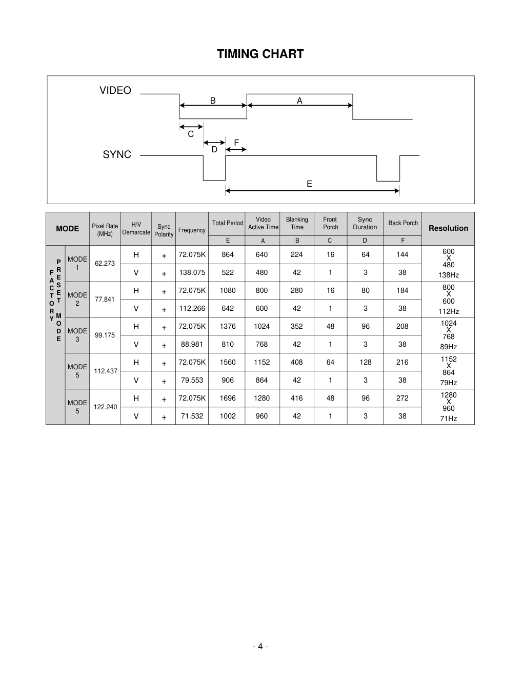
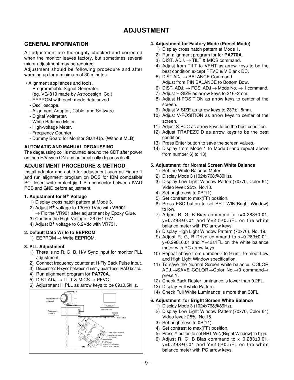
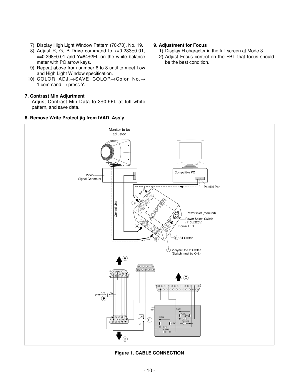
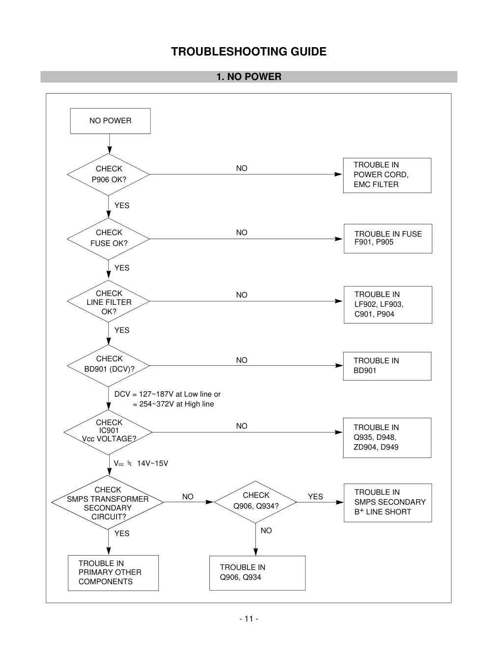
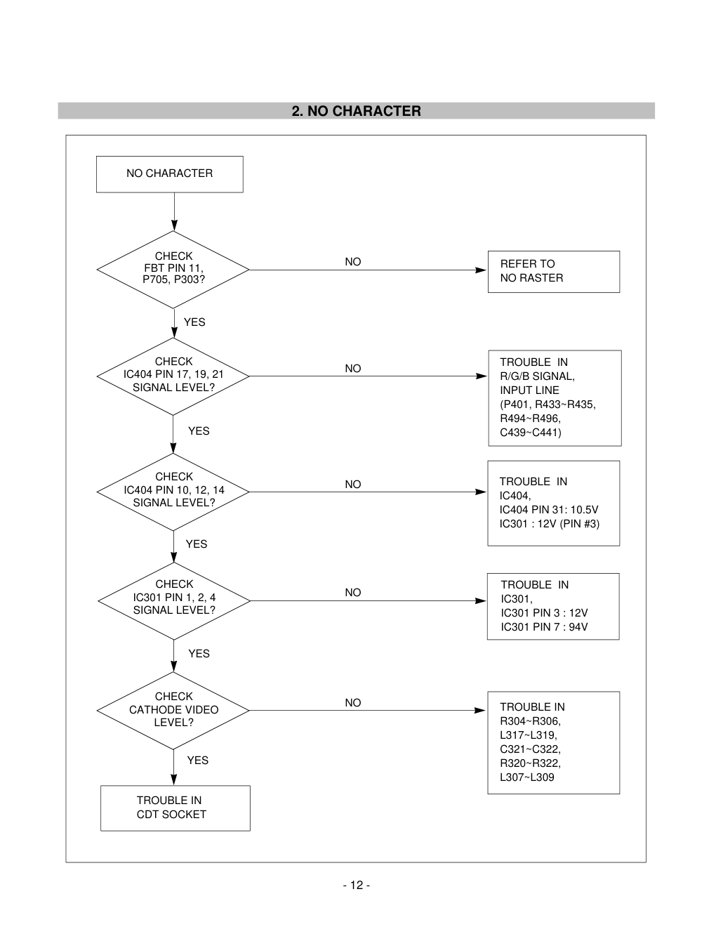
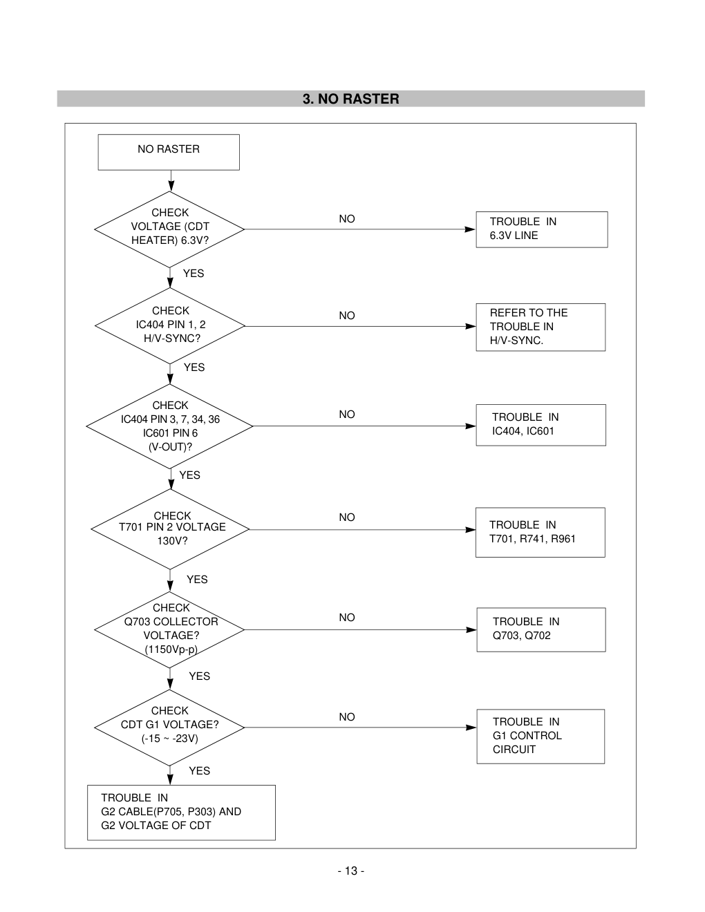
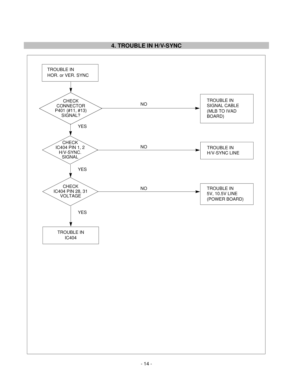
- 2 - 1. PICTURE TUBE Size : 17 inch (ez-Flat CDT) Gun : In-line DefIection Angle : 90° Neck Diameter : 29.1mm Dot Pitch : 0.25mm Face Treatment : Anti-Glare, Anti-Static & Anti-Reflection 2. SIGNAL 2-1. Horizontal & Vertical Sync 1) Input Voltage Level : Low=0~0.8V, High=2.1~5.5V 2) Sync Polarity : Positive or Negative 2-2. Video Input Signal 1) Voltage Level : 0.7V a) Color 0, 0 : 0Vp-p b) Color 7, 0 : 0.467Vp-p c) Color 15, 0 : 0.7Vp-p 2) Input Impedance : 75 Ω 3) Video Color : R, G, B Analog 4) Signal Format : Refer to the Timing Chart 2-3. Signal Connector 20 pin Connector 2-4. Scanning Frequency Horizontal : 72.075 kHz Vertical : 72/ 80/ 89/ 112/ 138 Hz 4. INPUT POWER 4-1. Power 1) 90~132Vrms (Low Line) 2) 180~264Vrms (High Line) 4-2. Frequency : 47~63 Hz Single Phase 4-3. Surge Voltage : 300 Vrms (100ms) 4-4. Peak Inrush Current: ≤ 100 Apk (All line condition) 4-5. Input Current : ≤ 4 Arm 4-6. Starting Voltage : 85Vrms min. 4-7. Power Consumption (with Dummy Board) 5. DISPLAY AREA 5-1. Active Video Area • Max Image Size - 325.1 x 243.8mm (12.80" x 9.60") • Preset Image Size - 316 x 237mm (12.44" x 9.33") 5-2. Display Color : Full Colors 5-3. Display Resolution : 1024 x 768 / 89Hz 5-4. Video Bandwidth : 99MHz 6. ENVIRONMENT 6-1. Operating Temperature: 10°C ~ 35°C (50°F ~ 95°F) (Ambient) 6-2. Relative Humidity : 20% ~ 95% (Non-condensing) 6-3. Operating altitude : 0~10,000 ft Shipping altitude : 0~15,000 ft 7. DIMENSIONS Width : 405.0 mm (15.94'') Depth : 406.0 mm (15.98'') Height : 405.0 mm (15.94'') 8. WEIGHT Net Weight : 14.9kg (32.85 lbs) Gross Weight : 103 kg (227.1 lbs.) SPECIFICATIONS MODE NORMAL (ON) LOW POWER POWER OFF LP/PWR-ON ON/ON OFF/ON OFF/OFF POWER CONSUMPTION less than 150 W less than 15 W less than 5 W 上海闵行晨辉电脑维修中心 TIMING CHART - 4 - VIDEO SYNC C E D F A B H/V Demarcate Pixel Rate (MHz) Sync Polarity Frequency Total Period Video Active Time Blanking Time Front Porch Sync Duration Back Porch Resolution E A B C D F MODE MODE 1 MODE 2 MODE 3 MODE 5 MODE 5 62.273 77.841 99.175 112.437 122.240 F A C T O R Y P R E S E T M O D E H V H V H V H V H V 72.075K 138.075 72.075K 112.266 72.075K 88.981 72.075K 79.553 72.075K 71.532 864 522 1080 642 1376 810 1560 906 1696 1002 640 480 800 600 1024 768 1152 864 1280 960 224 42 280 42 352 42 408 42 416 42 16 1 16 1 48 1 64 1 48 1 64 3 80 3 96 3 128 3 96 3 144 38 184 38 208 38 216 38 272 38 600 X 480 138Hz 800 X 600 112Hz 1024 X 768 89Hz 1152 X 864 79Hz 1280 X 960 71Hz + + + + + + + + + + CONTROL LOCATION - 5 - VR901: B Adjustment + VR731: EHT-COMP Adjustment FBT: Focus Adjustment GENERAL INFORMATION All adjustment are thoroughly checked and corrected when the monitor leaves factory, but sometimes several minor adjustment may be required. Adjustment should be following procedure and after warming up for a minimum of 30 minutes. • Alignment appliances and tools. - Programmable Signal Generator. (eg. VG-819 made by Astrodesign Co.) - EEPROM with each mode data saved. - Oscilloscope. - Alignment Adaptor, Cable, and Software. - Digital Voltmeter. - White Balance Meter. - High-voltage Meter. - Frequency Counter. - Dummy Board for Monitor Start-Up. (Without MLB) AUTOMATIC AND MANUAL DEGAUSSING The degaussing coil is mounted around the CDT after power on then H/V sync ON and automatically degauss itself. ADJUSTMENT PROCEDURE & METHOD Install adaptor and cable for adjustment such as Figure 1 and run alignment program on DOS for IBM compatible PC. Insert write protect jig 1 Pin connector between IVAD PCB and GND before adjustment. 1. Adjustment for B+ Voltage 1) Display cross hatch pattern at Mode 3. 2) Adjust B+ voltage to 130±0.1Vdc with VR901. → Fix the VR901 after adjustment by Epoxy Glue. 3) Confirm the High Voltage : 26.0±1.0kV. 4) Adjust B+ voltage to 6.2Vdc with VR731. 2. Default Data Write to EEPROM 1) EEPROM → Write EEPROM. 3. PLL Adjustment 1) There is no R, G, B, H/V Sync input for monitor PLL adjustment. 2) Connect frequency counter at H-Fly Back Pulse input. 3) Disconnect H-sync between dummy board and IVAD board. 4) Run alignment program for PA770A. 5) DIST.ADJ → TILT & MICS → PFVC. 6) Adjustment H PLL as arrow keys to be 69±0.5kHz. 4. Adjustment for Factory Mode (Preset Mode). 1) Display cross hatch pattern at Mode 1. 2) Run alignment program for for PA770A. 3) DIST. ADJ. → TILT & MICS command. 4) Adjust from TILT to VEHT as arrow keys to be the best condition except PFVC & V Blank DC. 5) DIST.ADJ.→ BALANCE Command. Adjust from PIN BALANCE to Bottom Bow. 6) DIST. ADJ. → FOS. ADJ → Mode No. → 1 command. 7) Adjust H-SIZE as arrow keys to 316±2mm. 8) Adjust H-POSITION as arrow keys to center of the screen. 9) Adjust V-SIZE as arrow keys to 237±1.5mm. 10) Adjust V-POSITION as arrow keys to center of the screen. 11) Adjust S-PCC as arrow keys to be the best condition. 12) Adjust TRAPEZOID as arrow keys to be the best condition. 13) Press Enter button to save the screen values. 14) Display from Mode 1 to Mode 5 and repeat above from number 6) to 13). 5. Adjustment for Normal Screen White Balance 1) Set the White Balance Meter. 2) Display Mode 3 (1024x768@89Hz). 3) Display Low Light Window Pattern(70x70, Color 64) Video level: 25%, No.18. 4) Set brightness to 0B(11). 5) Set contrast to max(FF) position. 6) Press ESC button to set BRT WIN(Bright Window) to low. 7) Adjust R, G, B Bias command to x=0.283±0.01, y=0.298±0.01 and Y=2.5±0.5FL on the white balance meter with PC arrow keys. 8) Display High Light Window Pattern (70x70), No. 19. 9) Adjust R, G, B Drive command to x=0.283±0.01, y=0.298±0.01 and Y=42±1FL on the white balance meter with PC arrow keys. 10) Repeat above from unmber 7 to 9 until to meet Low and High Light Window specification. 11) To save the Normal Screen white balance, COLOR ADJ.→SAVE COLOR→Color No.→0 command→ press Y. 12) Check Back Raster luminance is lower than 0.2FL. 13) Display Full white Pattern. 14) Check Full White Luminance is more than 38FL. 6. Adjustment for Bright Screen White Balance 1) Display Mode 3 (1024x768@89Hz). 2) Display Low Light Window Pattern(70x70, Color 64) Video level: 25%, No.18. 3) Set brightness to 0B(11). 4) Set contrast to max(FF) position. 5) Press Y button to set BRT WIN(Bright Window) to high. 6) Adjust R, G, B Bias command to x=0.283±0.01, y=0.298±0.01 and Y=2.5±0.5FL on the white balance meter with PC arrow keys. 220 Monitor to be adjusted Frequency Counter Compatible PC Parallel Port Power inlet (required) Power LED ST Switch Power Select Switch (110V/220V) Control Line Not used RS232C PARALLEL V-SYNC POWER ST VGS MONITOR E V-Sync On/Off Switch (Switch must be ON.) F A B C ADJUSTMENT - 9 - - 10 - Figure 1. CABLE CONNECTION 220 Monitor to be adjusted Video Signal Generator Compatible PC Parallel Port Power inlet (required) Power LED ST Switch Power Select Switch (110V/220V) Control Line Not used RS232C PARALLEL V-SYNC POWER ST VGS MONITOR E E V-Sync On/Off Switch (Switch must be ON.) F F A A B B C C 15 10 5 5 6 9 1 1 1 14 13 25 6 5V 5V 5V 4.7K 4.7K 4.7K 74LS06 74LS06 OFF ON OFF ON 11 7) Display High Light Window Pattern (70x70), No. 19. 8) Adjust R, G, B Drive command to x=0.283±0.01, x=0.298±0.01 and Y=84±2FL on the white balance meter with PC arrow keys. 9) Repeat above from unmber 6 to 8 until to meet Low and High Light Window specification. 10) COLOR ADJ.→SAVE COLOR→Color No.→ 1 command → press Y. 7. Contrast Min Adjurtment Adjust Contrast Min Data to 3±0.5FL at full white pattern, and save data. 8. Remove Write Protect jig from IVAD Ass’y 9. Adjustment for Focus 1) Display H character in the full screen at Mode 3. 2) Adjust Focus control on the FBT that focus should be the best condition. TROUBLESHOOTING GUIDE - 11 - 1. NO POWER NO POWER TROUBLE IN POWER CORD, EMC FILTER TROUBLE IN FUSE F901, P905 TROUBLE IN BD901 TROUBLE IN Q935, D948, ZD904, D949 TROUBLE IN SMPS SECONDARY B+ LINE SHORT TROUBLE IN Q906, Q934 TROUBLE IN PRIMARY OTHER COMPONENTS CHECK P906 OK? CHECK FUSE OK? CHECK BD901 (DCV)? CHECK IC901 Vcc VOLTAGE? CHECK Q906, Q934? CHECK SMPS TRANSFORMER SECONDARY CIRCUIT? NO YES YES YES YES NO NO NO NO NO DCV = 127~187V at Low line or = 254~372V at High line Vcc ≒ 14V~15V TROUBLE IN LF902, LF903, C901, P904 CHECK LINE FILTER OK? YES NO - 12 - 2. NO CHARACTER NO CHARACTER TROUBLE IN CDT SOCKET CHECK FBT PIN 11, P705, P303? CHECK IC404 PIN 17, 19, 21 SIGNAL LEVEL? CHECK IC404 PIN 10, 12, 14 SIGNAL LEVEL? CHECK IC301 PIN 1, 2, 4 SIGNAL LEVEL? CHECK CATHODE VIDEO LEVEL? REFER TO NO RASTER TROUBLE IN R/G/B SIGNAL, INPUT LINE (P401, R433~R435, R494~R496, C439~C441) TROUBLE IN IC404, IC404 PIN 31: 10.5V IC301 : 12V (PIN #3) TROUBLE IN IC301, IC301 PIN 3 : 12V IC301 PIN 7 : 94V TROUBLE IN R304~R306, L317~L319, C321~C322, R320~R322, L307~L309 NO NO NO NO NO YES YES YES YES YES - 13 - 3. NO RASTER CHECK VOLTAGE (CDT HEATER) 6.3V? CHECK IC404 PIN 1, 2 H/V-SYNC? CHECK IC404 PIN 3, 7, 34, 36 IC601 PIN 6 (V-OUT)? CHECK T701 PIN 2 VOLTAGE 130V? CHECK Q703 COLLECTOR VOLTAGE? (1150Vp-p) CHECK CDT G1 VOLTAGE? (-15 ~ -23V) NO RASTER TROUBLE IN G2 CABLE(P705, P303) AND G2 VOLTAGE OF CDT TROUBLE IN 6.3V LINE REFER TO THE TROUBLE IN H/V-SYNC. TROUBLE IN IC404, IC601 TROUBLE IN T701, R741, R961 TROUBLE IN Q703, Q702 TROUBLE IN G1 CONTROL CIRCUIT NO NO NO NO NO NO YES YES YES YES YES YES - 14 - 4. TROUBLE IN H/V-SYNC CHECK CONNECTOR P401 (#11, #13) SIGNAL? CHECK IC404 PIN 1, 2 H/V-SYNC. SIGNAL CHECK IC404 PIN 28, 31 VOLTAGE TROUBLE IN HOR. or VER. SYNC TROUBLE IN SIGNAL CABLE (MLB TO IVAD BOARD) TROUBLE IN H/V-SYNC LINE TROUBLE IN 5V, 10.5V LINE (POWER BOARD) TROUBLE IN IC404 NO NO NO YES YES YES - 7 - BLOCK DIAGRAM Video Output Amplifier (IC301) R G B CDT 6.3V HEATER 12 V 94 V DY SCREEN FOCUS V-DY H-DY H.V FLY BACK TRANS (T701) ABL & Beam Feedback & X-ray 130V Vertical Output IC (IC601) HDT(T702) 12 V H-out TR 2SC5589 12V SMPS Trans (T901) & Main power Control IC (IC901) AC INLET 90~132Vac with P902 and 180~264Vac without P902 3.3V 5V 2.5V TO MLB MLB Power Module E_PROM (IC401) T5V 20 Vdc H-FBP IVAD Controller (IV402,IC403,IC404) (Video pre-Amp & H/V Processor & Micom interface) 10.5 V R-Video G-Video B-Video Power_On LP SCL SDA H-Sync V-Sync -10 V Cut-Off Control (Q301~Q306) T5V G1 -90V Blanking & Bright Control 131V 15V 12V -10V 94V BEAM_FB FROM MLB Vref V-Drive -90V DCO Protection DCO Protection LP Power-on Sync IVAD Board Video Board D/Converter Board Analog Board V-DY H-DY Line Filter Degaussing Circuit Degaussing Coil 12V Tilt Control Circuit 6.3 V 12 V Tilt Coil Tilt 20V Audio 12V CPU 12V 6.3V Dynamic Focus Circuit (T745,Q704) H-Linearity Circuit (L702) 253V 12V EHT-COMP T5 V H-Drive LP Power-on DESCRIPTION OF BLOCK DIAGRAM - 8 - 1. Line Filter & Associated Circuit This is used for suppressing noise of power input line flowing into the monitor and/or some noise generated in this monitor flowing out through the power input line. That is to say, this circuit prevents interference between the monitor and other electric appliances. 2. Degauss Circuit & Coil The degauss circuit consists of the degaussing coil, the PTC (Positive Temperature Coefficient) thermistor (TH901) and the relay (RL901). This circuit eliminates abnormal color of the screen automatically by degaussing the shadow mask in the CDT during turning on the power switch. 3. SMPS (Switching Mode Power Supply) This circuit working of 90~132VAC (low line) with P902 and 180~264VAC(high line) without P902 (47~63Hz). The operation procedure is as belows: (1) AC input voltage is rectified and smoothed by the bridge diode (BD901) and rectified capacitor (C905,C967). (2) The rectified voltage (DC) is applied to the primary of the transformer (T901). (3) The control IC (IC901) generates switching pulse to turn on and off the primary coil of the transformer (T901) repeatedly. (4) Depending on turn ratio of the transforner, the secondary voltages are rectified by each diode (D901, D902, D925, D926, D931~D934, D940) and operate others circuit (Horizontal, Vertical deflection, Video amplifier etc ...) 4. Down Converter This circuit is DC/DC converter which generates +5V, +3.3V, +2.5V. It receives +20V from analog board. It’s used 2 chanel DC/DC converter controller, outputs +5V, +3.3V. Linear regulator(IC807, FAN1582) provided +3.3V outputs +2.5V. Output voltages are controlled by DCO(Down converter off) signal. If DCO signal is low, enables output voltage. If DCO signal is high, disables output voltage. 5. Power Management Circuit This circuit control power consumption of the monitor by detecting LP and PWR-ON signal. There are LP and power off mode. 1) LP mode. When LP signal input, the circuit consists of Q932 and others become LP mode. LP mode’s power consumption is below 15W. (With dummy board) 2) Power off mode. When PWR-ON signal input, power off mode operation is the same as LP mode and 6.3V voltage is controlled by Q933, and Down Converter become off. 6. X-ray Protection. This circuit detects the rectified DC voltage come from the FBT pin 1, if the high voltage of the FBT goes up to 29kV (abnormal state), the output voltage of FBT pin 1 is increasing too, It turn on the zener diode (ZD701) and Q709. Then IC404 (IVAD2) pin 20 is shut down, H-Drive not generated and high voltage not generated. (In normal state, high voltage is about 26kV) 7. Horizontal and Vertical Oscillation. This circuit generates the horizontal pulse and the vertical pulse by taking the H and V sync signal. This circuit consists of the IVAD2 (IC404) and associated circuit. 8. Horizontal Deflection Output Circuit. This circuit makes the horizontal deflection by supplying the saw-tooth current to the horizontal deflection yoke. 9. High Voltage Output & FBT (Flyback Transformer). The high voltage output circuit is used for generating pulse to the primary coil of the FBT (Flyback Transformer :T701). A boosted voltage -about 26kV - appears at the secondary of the FBT and it is supplied to the anode of the CDT. And there are other output voltages such as the focus and the screen voltage. 10. H-Linearity Coil. (L702) This coil corrects the horizontal linearity for each horizontal sync frequency. 11. Vertical Output circuit. This circuit takes the vertical ramp wave from the IVAD2 (IC404) and performs the vertical deflection by supplying the saw-tooth current to the vertical deflection yoke. 12. Image Rotation (Tilt) Circuit. This circuit corrects the tilt of the screen by supplying the image rotation signal to the tilt coil which is attached near the deflection yoke of the CDT. 13. Video Pre-Amp Circuit. This circuit amplifies the analog video signal from 0- 0.7V to 0-4V. It is operated by taking the clamp, R, G, B drives, and contrast signals from the MLB. 14. Video Output Circuit. This circuit amplifies the video signal which comes from the video pre-amp circuit and amplified video signal is applied to the CDT cathode. WIRING DIAGRAM - 6 - P503 P506 P501 P507 P505 P504 CN902 CN901 P403 P703 P601 P902 P996 P901 P701 - 25 - - 26 - ANALOG SCHEMATIC DIAGRAM SCHEMATIC DIAGRAM 上海闵行晨辉电脑维修中心 - 27 - - 28 - NOTICE Since this is a basic schematic diagram. The value of components and some partial connection are sucject to be changed for improvement without notice. VIDEO SCHEMATIC DIAGRAM DOWN CONVERTER SCHEMATIC DIAGRAM IVAD SCHEMATIC DIAGRAM 上海闵行晨辉电脑维修中心 EXPLODED VIEW 1 2 3 4 5 6 7 8 9 10 11 12 13 14 15 17 18 19 20 21 22 23 24 25 16 EXPLODED VIEW PARTS LIST NO 1 2 3 4 5 6 7 8 9 10 11 12 13 14 15 16 17 18 19 20 21 22 23 24 25 PART NO. 6318L17003E 4951TKS080A 1SZZTMF005A 6140TC4004A 6868T17008A 4810TKK196A 4810TKK197A 4950TKK399A 5410TKK028A 4815TKK023A 4815TKK021A 4951TKK076A 6631T25016A 6631T25017A 6871TST280A 6850TAC003A or 6850TAC003C 4950TKK434A 4810TKK201A 6631T20017A or 6631T20017C 6871TMT280A 4920TKC045A 4920TKC046A 6871TVT280A 6850TAC004A or 6850TAC004C 6631T20017B or 6631T20017D DESCRIPTION CDT(CIRC), M41QEE903X 05NLGD LG-PHILIPS 70KHZ 29.1MM FLAT TCO METAL ASSEMBLY, FRAME SCREW,DRAWING , D6.0 L11.0 MSWR/FZMCW1 COIL,DEGAUSSING, LX31 GET D-COIL,0.4*120TS,1260,PA770A CABLE ASS’Y, CDT EARTH BRACKET, SUPPORTER GUSSET LEFT BRACKET, SUPPORTER GUSSET RIGHT METAL, BASE AC FILTER BD INSULATION, PC SHEET AC FILTER BD SHIELD ASSEMBLY, SIDE(620-XXXX)AC INNER FOR P62 SHIELD ASSEMBLY, SIDE AC FILTER FOR P62 METAL ASSEMBLY, FRAME DIVIDER PANEL FOR P62 CONNECTOR ASSEMBLY, 20P H-H 90MM UL 1061 AWG 22 TWI PA770A CONNECTOR ASSEMBLY 20P H-H 330MM UL 2405 AWG 26-2C PA770A PWB(PCB) ASSEMBLY,SUB PA770A.XHGM IVAD SUB TOTAL APPLE CA-107 CABLE,D-SUB, UL2990-15C(7.5) AT 110MM BLACK(9930) PA770A CABLE,D-SUB, UL2990-15C97.50AT 110MM BLACK(9930) PA770A (YH) METAL SUPPORT CLIP IVAD TO VIDEO CABLE BRACKET, HOLDER CLIP IVAD WIRE-ANALOG FOR P62 CONNECTOR ASSEMBLY, 18P H-H 175MM UL1007#28 PA770A CONNECTOR ASSEMBLY, 18P H-H 175MM UL1007#28 YEONHO PWB(PCB) ASSEMBLY,MAIN, PA770A ANALOG APPLE CA-107 TOTAL HEAT SINK, 90.60*102.03*46.71 AL ,P62 HEAT SINK, 96.30*102.30*47.73 AL , P62 PWB(PCB) ASSEMBLY,VIDEO, PA770A XHGM VIDEO TOTAL APPLE CA-107 CABLE,D-SUB, UL 2990-9C AT 170MM BLACK(9930) PA770A(IVAD-VIDEO) CABLE,D-SUB, UL 2990-9C AT 170MM BLACK(9930) PA770A (YH) CONNECTOR ASSEMBLY, 7P H-H 210MM UL1061 AWG 26 TWI 590-5108 PA770A CONNECTOR ASSEMBLY, 7P H-H 210MM UL1061 AWG 26 TWI TEONHO APPLE Part No. 600-9565 620-1916 452-0217 870-1022 592-0018 815-6762 815-6763 805-3375 815-6617 805-3615 805-3322 620-1926 590-5094 590-5093 600-9560 590-5228 590-5110 805-3624 815-6830 590-5096 590-5096 600-9567 805-3316 805-3313 590-5099 590-5109 590-5109 590-5108 590-5108 Note: Safety Mark
版权声明
1. 本站所有素材,仅限学习交流,仅展示部分内容,如需查看完整内容,请下载原文件。
2. 会员在本站下载的所有素材,只拥有使用权,著作权归原作者所有。
3. 所有素材,未经合法授权,请勿用于商业用途,会员不得以任何形式发布、传播、复制、转售该素材,否则一律封号处理。
4. 如果素材损害你的权益请联系客服QQ:77594475 处理。