LG L2300C液晶显示器维修手册和图纸
 "LG L2300C液晶显示器维修手册和图纸-0")
 "LG L2300C液晶显示器维修手册和图纸-1")
 "LG L2300C液晶显示器维修手册和图纸-2")
 "LG L2300C液晶显示器维修手册和图纸-3")
 "LG L2300C液晶显示器维修手册和图纸-4")
 "LG L2300C液晶显示器维修手册和图纸-5")
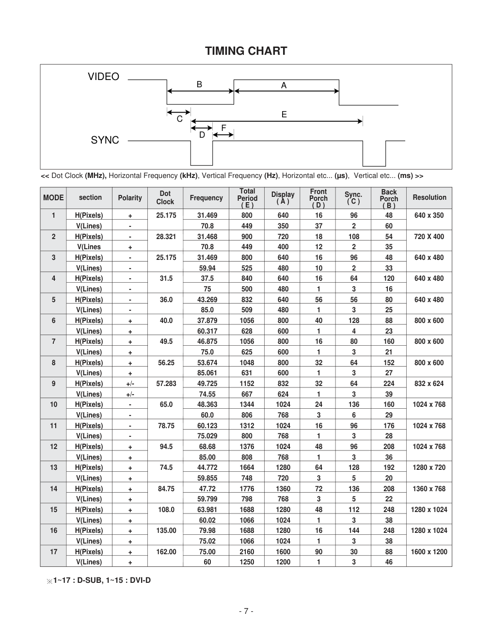 "LG L2300C液晶显示器维修手册和图纸-6")
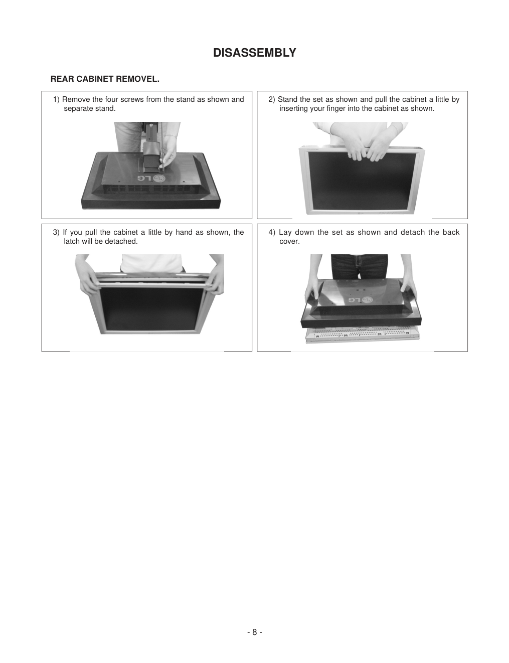 "LG L2300C液晶显示器维修手册和图纸-7")
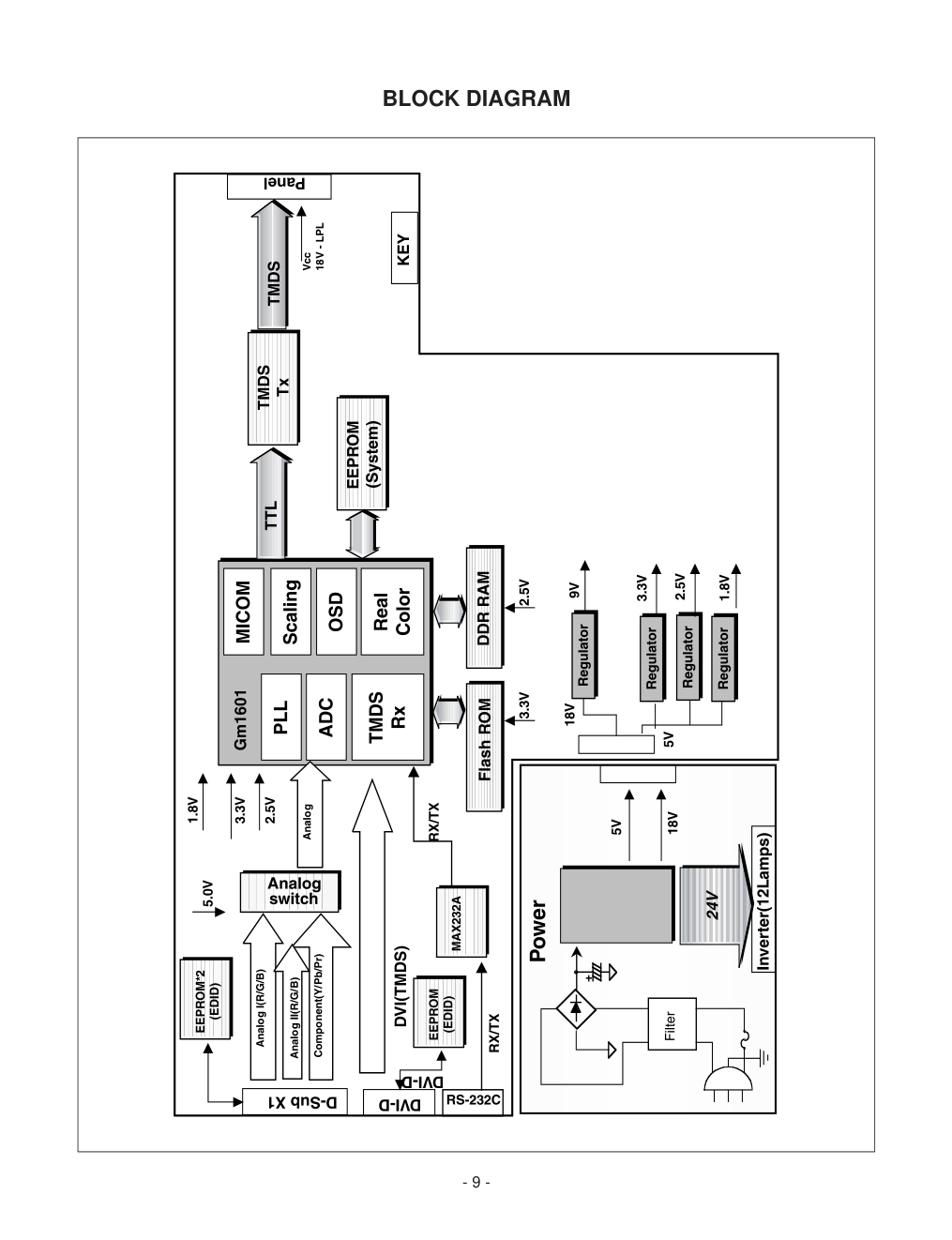 "LG L2300C液晶显示器维修手册和图纸-8")
 "LG L2300C液晶显示器维修手册和图纸-9")
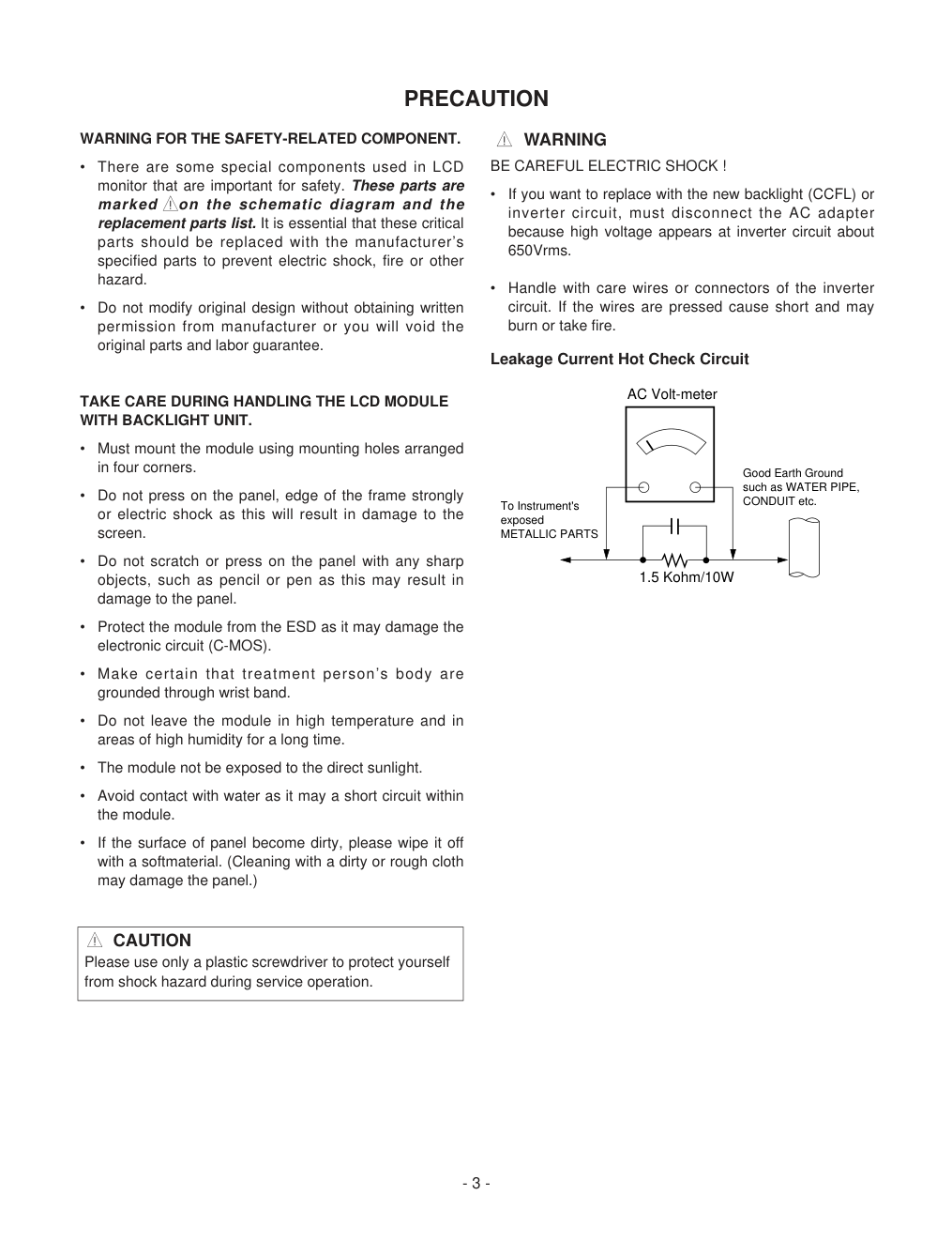
COLOR MONITOR SERVICE MANUAL Website:http://biz.LGservice.com E-mail:http://www.LGEservice.com/techsup.html CAUTION BEFORE SERVICING THE UNIT, READ THE SAFETY PRECAUTIONS IN THIS MANUAL. CHASSIS NO. : CL-77 MODEL: L2300C (L2300CN.AL**LF) MODEL: L2300C (L2300CKN.AL**LF) ( ) **Same model for Service 1. LCD CHARACTERISTICS Type : TFT Color LCD Module Active Display Area : 23.01 inch Pixel Pitch : 0.258 (H) x 0.258(V) Size : 559.8 (H) x 333.8 (V) x 45.7 (D) Color Depth : 16.777,216 colors / 8Bit Electrical Interface : LVDS Surface Treatment : Anti-Glare, Hard-coating(3H) Operating Mode : Normally Black Backlight Unit : 6 CCFL 2. OPTICAL CHARACTERISTICS 2-1. Viewing Angle by Contrast Ratio ≥ 10 Left : -88(Typ) Right : +88°(Typ) Top :+88° (Typ) Bottom : -88°(Typ) 2-2. Luminance : 500(Typ) 2-3. Contrast Ratio : 550(Typ) 3. SIGNAL (Refer to the Timing Chart) 3-1. Sync Signal • Type : Separate Sync, Digitala SOG (Sync On Green) Composite Sync 3-2. Video Input Signal 1) Type : R, G, B Analog 2) Voltage Level : 0~0.71 V a) Color 0, 0 : 0 Vp-p b) Color 7, 0 : 0.467 Vp-p c) Color 15, 0 : 0.714 Vp-p 3) Input Impedance : 75 Ω 3-4. Operating Frequency Analog Horizontal : 30 ~ 83kHz Vertical : 56 ~ 85Hz Dot clock:< 160MHz Digital Horizontal : 30 ~ 72kHz Vertical : 56 ~ 85Hz Dot clock:< 160MHz 4. Max. Resolution Analog : 1600 x 1200 / 60Hz Digital : 1280 x 1024 / 60Hz 5. POWER SUPPLY 5-1. Power : AC 100-240V~, 50/60Hz , 1.2A 5-2. Power Consumption 6. ENVIRONMENT 6-1. Operating Temperature : 10°C~35°C (50°F~95°F) 6-2. Relative Humidity : 10%~80% (Non-condensing) 6-3. Lamp Life : 40,000 Hours(Min) 7. DIMENSIONS (with TILT/SWIVEL) Width : 446 mm (17.56'') Depth : 237.3 mm (9.34'') Height : 445.6 mm (17.54'') 8. WEIGHT (with TILT/SWIVEL) Net. Weight : 9.42 kg (20.77lbs) Gross Weight : 12.28 kg (27.08lbs) CONTENTS SPECIFICATIONS - 2 - SPECIFICATIONS ................................................... 2 PRECAUTIONS ....................................................... 3 TIMING CHART ....................................................... 7 DISASSEMBLY ....................................................... 8 BLOCK DIAGRAM ................................................... 9 DESCRIPTION OF BLOCK DIAGRAM...................10 ADJUSTMENT ...................................................... 12 TROUBLESHOOTING GUIDE .............................. 14 WIRING DIAGRAM ............................................... 18 EXPLODED VIEW...................................................19 REPLACEMENT PARTS LIST ...............................21 SCHEMATIC DIAGRAM......................................... 26 H/V SYNC ON/ON OFF/ON ON/OFF OFF/OFF - POWER CONSUMPTION less than 90 W less than 2W less than 2W less than 2W less than 2W LED COLOR GREEN AMBER OFF VIDEO ACTIVE OFF OFF OFF - MODE POWER ON(NORMAL) STAND BY SUSPEND DPMS OFF POWER S/W OFF - 3 - PRECAUTION WARNING FOR THE SAFETY-RELATED COMPONENT. • There are some special components used in LCD monitor that are important for safety. These parts are marked on the schematic diagram and the replacement parts list. It is essential that these critical parts should be replaced with the manufacturer’s specified parts to prevent electric shock, fire or other hazard. • Do not modify original design without obtaining written permission from manufacturer or you will void the original parts and labor guarantee. TAKE CARE DURING HANDLING THE LCD MODULE WITH BACKLIGHT UNIT. • Must mount the module using mounting holes arranged in four corners. • Do not press on the panel, edge of the frame strongly or electric shock as this will result in damage to the screen. • Do not scratch or press on the panel with any sharp objects, such as pencil or pen as this may result in damage to the panel. • Protect the module from the ESD as it may damage the electronic circuit (C-MOS). • Make certain that treatment person’s body are grounded through wrist band. • Do not leave the module in high temperature and in areas of high humidity for a long time. • The module not be exposed to the direct sunlight. • Avoid contact with water as it may a short circuit within the module. • If the surface of panel become dirty, please wipe it off with a softmaterial. (Cleaning with a dirty or rough cloth may damage the panel.) WARNING BE CAREFUL ELECTRIC SHOCK ! • If you want to replace with the new backlight (CCFL) or inverter circuit, must disconnect the AC adapter because high voltage appears at inverter circuit about 650Vrms. • Handle with care wires or connectors of the inverter circuit. If the wires are pressed cause short and may burn or take fire. Leakage Current Hot Check Circuit CAUTION Please use only a plastic screwdriver to protect yourself from shock hazard during service operation. 1.5 Kohm/10W To Instrument's exposed METALLIC PARTS Good Earth Ground such as WATER PIPE, CONDUIT etc. AC Volt-meter - 4 - SERVICING PRECAUTIONS CAUTION: Before servicing receivers covered by this service manual and its supplements and addenda, read and follow the SAFETY PRECAUTIONS on page 3 of this publication. NOTE: If unforeseen circumstances create conflict between the following servicing precautions and any of the safety precautions on page 3 of this publication, always follow the safety precautions. Remember: Safety First. General Servicing Precautions 1. Always unplug the receiver AC power cord from the AC power source before; a. Removing or reinstalling any component, circuit board module or any other receiver assembly. b. Disconnecting or reconnecting any receiver electrical plug or other electrical connection. c. Connecting a test substitute in parallel with an electrolytic capacitor in the receiver. CAUTION: A wrong part substitution or incorrect polarity installation of electrolytic capacitors may result in an explosion hazard. d. Discharging the picture tube anode. 2. Test high voltage only by measuring it with an appropriate high voltage meter or other voltage measuring device (DVM, FETVOM, etc) equipped with a suitable high voltage probe. Do not test high voltage by "drawing an arc". 3. Discharge the picture tube anode only by (a) first connecting one end of an insulated clip lead to the degaussing or kine aquadag grounding system shield at the point where the picture tube socket ground lead is connected, and then (b) touch the other end of the insulated clip lead to the picture tube anode button, using an insulating handle to avoid personal contact with high voltage. 4. Do not spray chemicals on or near this receiver or any of its assemblies. 5. Unless specified otherwise in this service manual, clean electrical contacts only by applying the following mixture to the contacts with a pipe cleaner, cotton- tipped stick or comparable non-abrasive applicator; 10% (by volume) Acetone and 90% (by volume) isopropyl alcohol (90%-99% strength) CAUTION: This is a flammable mixture. Unless specified otherwise in this service manual, lubrication of contacts in not required. 6. Do not defeat any plug/socket B+ voltage interlocks with which receivers covered by this service manual might be equipped. 7. Do not apply AC power to this instrument and/or any of its electrical assemblies unless all solid-state device heat sinks are correctly installed. 8. Always connect the test receiver ground lead to the receiver chassis ground before connecting the test receiver positive lead. Always remove the test receiver ground lead last. 9. Use with this receiver only the test fixtures specified in this service manual. CAUTION: Do not connect the test fixture ground strap to any heat sink in this receiver. Electrostatically Sensitive (ES) Devices Some semiconductor (solid-state) devices can be damaged easily by static electricity. Such components commonly are called Electrostatically Sensitive (ES) Devices. Examples of typical ES devices are integrated circuits and some field-effect transistors and semiconductor "chip" components. The following techniques should be used to help reduce the incidence of component damage caused by static by static electricity. 1. Immediately before handling any semiconductor component or semiconductor-equipped assembly, drain off any electrostatic charge on your body by touching a known earth ground. Alternatively, obtain and wear a commercially available discharging wrist strap device, which should be removed to prevent potential shock reasons prior to applying power to the unit under test. 2. After removing an electrical assembly equipped with ES devices, place the assembly on a conductive surface such as aluminum foil, to prevent electrostatic charge buildup or exposure of the assembly. 3. Use only a grounded-tip soldering iron to solder or unsolder ES devices. 4. Use only an anti-static type solder removal device. Some solder removal devices not classified as "anti- static" can generate electrical charges sufficient to damage ES devices. 5. Do not use freon-propelled chemicals. These can generate electrical charges sufficient to damage ES devices. 6. Do not remove a replacement ES device from its protective package until immediately before you are ready to install it. (Most replacement ES devices are packaged with leads electrically shorted together by conductive foam, aluminum foil or comparable conductive material). 7. Immediately before removing the protective material from the leads of a replacement ES device, touch the protective material to the chassis or circuit assembly into which the device will be installed. CAUTION: Be sure no power is applied to the chassis or circuit, and observe all other safety precautions. 8. Minimize bodily motions when handling unpackaged replacement ES devices. (Otherwise harmless motion such as the brushing together of your clothes fabric or the lifting of your foot from a carpeted floor can generate static electricity sufficient to damage an ES device.) - 5 - General Soldering Guidelines 1. Use a grounded-tip, low-wattage soldering iron and appropriate tip size and shape that will maintain tip temperature within the range or 500 F to 600 F. 2. Use an appropriate gauge of RMA resin-core solder composed of 60 parts tin/40 parts lead. 3. Keep the soldering iron tip clean and well tinned. 4. Thoroughly clean the surfaces to be soldered. Use a mall wire-bristle (0.5 inch, or 1.25cm) brush with a metal handle. Do not use freon-propelled spray-on cleaners. 5. Use the following unsoldering technique a. Allow the soldering iron tip to reach normal temperature. (500 F to 600 F) b. Heat the component lead until the solder melts. c. Quickly draw the melted solder with an anti-static, suction-type solder removal device or with solder braid. CAUTION: Work quickly to avoid overheating the circuitboard printed foil. 6. Use the following soldering technique. a. Allow the soldering iron tip to reach a normal temperature (500 F to 600 F) b. First, hold the soldering iron tip and solder the strand against the component lead until the solder melts. c. Quickly move the soldering iron tip to the junction of the component lead and the printed circuit foil, and hold it there only until the solder flows onto and around both the component lead and the foil. CAUTION: Work quickly to avoid overheating the circuit board printed foil. d. Closely inspect the solder area and remove any excess or splashed solder with a small wire-bristle brush. IC Remove/Replacement Some chassis circuit boards have slotted holes (oblong) through which the IC leads are inserted and then bent flat against the circuit foil. When holes are the slotted type, the following technique should be used to remove and replace the IC. When working with boards using the familiar round hole, use the standard technique as outlined in paragraphs 5 and 6 above. Removal 1. Desolder and straighten each IC lead in one operation by gently prying up on the lead with the soldering iron tip as the solder melts. 2. Draw away the melted solder with an anti-static suction-type solder removal device (or with solder braid) before removing the IC. Replacement 1. Carefully insert the replacement IC in the circuit board. 2. Carefully bend each IC lead against the circuit foil pad and solder it. 3. Clean the soldered areas with a small wire-bristle brush. (It is not necessary to reapply acrylic coating to the areas). "Small-Signal" Discrete Transistor Removal/Replacement 1. Remove the defective transistor by clipping its leads as close as possible to the component body. 2. Bend into a "U" shape the end of each of three leads remaining on the circuit board. 3. Bend into a "U" shape the replacement transistor leads. 4. Connect the replacement transistor leads to the corresponding leads extending from the circuit board and crimp the "U" with long nose pliers to insure metal to metal contact then solder each connection. Power Output, Transistor Device Removal/Replacement 1. Heat and remove all solder from around the transistor leads. 2. Remove the heat sink mounting screw (if so equipped). 3. Carefully remove the transistor from the heat sink of the circuit board. 4. Insert new transistor in the circuit board. 5. Solder each transistor lead, and clip off excess lead. 6. Replace heat sink. Diode Removal/Replacement 1. Remove defective diode by clipping its leads as close as possible to diode body. 2. Bend the two remaining leads perpendicular y to the circuit board. 3. Observing diode polarity, wrap each lead of the new diode around the corresponding lead on the circuit board. 4. Securely crimp each connection and solder it. 5. Inspect (on the circuit board copper side) the solder joints of the two "original" leads. If they are not shiny, reheat them and if necessary, apply additional solder. Fuse and Conventional Resistor Removal/Replacement 1. Clip each fuse or resistor lead at top of the circuit board hollow stake. 2. Securely crimp the leads of replacement component around notch at stake top. 3. Solder the connections. CAUTION: Maintain original spacing between the replaced component and adjacent components and the circuit board to prevent excessive component temperatures. - 6 - Circuit Board Foil Repair Excessive heat applied to the copper foil of any printed circuit board will weaken the adhesive that bonds the foil to the circuit board causing the foil to separate from or "lift-off" the board. The following guidelines and procedures should be followed whenever this condition is encountered. At IC Connections To repair a defective copper pattern at IC connections use the following procedure to install a jumper wire on the copper pattern side of the circuit board. (Use this technique only on IC connections). 1. Carefully remove the damaged copper pattern with a sharp knife. (Remove only as much copper as absolutely necessary). 2. carefully scratch away the solder resist and acrylic coating (if used) from the end of the remaining copper pattern. 3. Bend a small "U" in one end of a small gauge jumper wire and carefully crimp it around the IC pin. Solder the IC connection. 4. Route the jumper wire along the path of the out-away copper pattern and let it overlap the previously scraped end of the good copper pattern. Solder the overlapped area and clip off any excess jumper wire. At Other Connections Use the following technique to repair the defective copper pattern at connections other than IC Pins. This technique involves the installation of a jumper wire on the component side of the circuit board. 1. Remove the defective copper pattern with a sharp knife. Remove at least 1/4 inch of copper, to ensure that a hazardous condition will not exist if the jumper wire opens. 2. Trace along the copper pattern from both sides of the pattern break and locate the nearest component that is directly connected to the affected copper pattern. 3. Connect insulated 20-gauge jumper wire from the lead of the nearest component on one side of the pattern break to the lead of the nearest component on the other side. Carefully crimp and solder the connections. CAUTION: Be sure the insulated jumper wire is dressed so the it does not touch components or sharp edges. - 7 - TIMING CHART VIDEO SYNC B D C F E A << Dot Clock (MHz), Horizontal Frequency (kHz), Vertical Frequency (Hz), Horizontal etc... (µs), Vertical etc... (ms) >> MODE section Polarity Frequency Total Period ( E ) Display ( A ) Front Porch ( D ) Sync. ( C ) Back Porch ( B ) Resolution Dot Clock 1 H(Pixels) + 25.175 31.469 800 640 16 96 48 640 x 350 V(Lines) - 70.8 449 350 37 2 60 2 H(Pixels) - 28.321 31.468 900 720 18 108 54 720 X 400 V(Lines + 70.8 449 400 12 2 35 3 H(Pixels) - 25.175 31.469 800 640 16 96 48 640 x 480 V(Lines) - 59.94 525 480 10 2 33 4 H(Pixels) - 31.5 37.5 840 640 16 64 120 640 x 480 V(Lines) - 75 500 480 1 3 16 5 H(Pixels) - 36.0 43.269 832 640 56 56 80 640 x 480 V(Lines) - 85.0 509 480 1 3 25 6 H(Pixels) + 40.0 37.879 1056 800 40 128 88 800 x 600 V(Lines) + 60.317 628 600 1 4 23 7 H(Pixels) + 49.5 46.875 1056 800 16 80 160 800 x 600 V(Lines) + 75.0 625 600 1 3 21 8 H(Pixels) + 56.25 53.674 1048 800 32 64 152 800 x 600 V(Lines) + 85.061 631 600 1 3 27 9 H(Pixels) +/- 57.283 49.725 1152 832 32 64 224 832 x 624 V(Lines) +/- 74.55 667 624 1 3 39 10 H(Pixels) - 65.0 48.363 1344 1024 24 136 160 1024 x 768 V(Lines) - 60.0 806 768 3 6 29 11 H(Pixels) - 78.75 60.123 1312 1024 16 96 176 1024 x 768 V(Lines) - 75.029 800 768 1 3 28 12 H(Pixels) + 94.5 68.68 1376 1024 48 96 208 1024 x 768 V(Lines) + 85.00 808 768 1 3 36 13 H(Pixels) + 74.5 44.772 1664 1280 64 128 192 1280 x 720 V(Lines) + 59.855 748 720 3 5 20 14 H(Pixels) + 84.75 47.72 1776 1360 72 136 208 1360 x 768 V(Lines) + 59.799 798 768 3 5 22 15 H(Pixels) + 108.0 63.981 1688 1280 48 112 248 1280 x 1024 V(Lines) + 60.02 1066 1024 1 3 38 16 H(Pixels) + 135.00 79.98 1688 1280 16 144 248 1280 x 1024 V(Lines) + 75.02 1066 1024 1 3 38 17 H(Pixels) + 162.00 75.00 2160 1600 90 30 88 1600 x 1200 V(Lines) + 60 1250 1200 1 3 46 1~17 : D-SUB, 1~15 : DVI-D - 8 - DISASSEMBLY REAR CABINET REMOVEL. 1) Remove the four screws from the stand as shown and separate stand. 2) Stand the set as shown and pull the cabinet a little by inserting your finger into the cabinet as shown. 3) If you pull the cabinet a little by hand as shown, the latch will be detached. 4) Lay down the set as shown and detach the back cover. - 9 - BLOCK DIAGRAM - 10 - DESCRIPTION OF BLOCK DIAGRAM 1. Video Controller Part & Display Data Transmitter Part. This part amplifies the level of video signal for the digital conversion and converts from the analog video signal to the digital video signal using a pixel clock. The pixel clock for each mode is generated by the PLL. The range of the pixel clock is from 25MHz to 165MHz. This part consists of the Scaler, Flash-ROM IC which stores program data, Reset IC. The Scaler gets the video signal converted analog to digital, interpolates input to 1920 x 1200 resolution signal and outputs 8-bit R, G, B signal to transmitter. Especially pre-amp / ADC / Video controller/ Transmitter are merged to one chip 'Gm1601' by Genesis. This part transmit digital signal from the Scaler to the receiver of module. 2. Power Part This part consists of the two 3.3V and one 2.5V and one 1.8Vregulators to convert power which is provided 18V in Power Board V is provided for LCD Panel. 24V in Power Board V is provided for Inverter Part. Also, 5V is converted 3.3V and 2.5V and 1.8V by regulator. Converted power is provided for IC in the main board. - 11 - EMI COMPONENTS LINE 100 ~ 240V INPUT RECTIFIER AND FILTER ENERGY TRANSFER OUTPUT RECTIFIER AND FILTER 18V 5V GND SIGNAL COLLECTI ON PHOTO- COUPLER ISOLATION PWM CONTROL CIRCUIT HVDC 100KHz PRIMARY SECONDARY 50 ~ 60Hz Operation description_POWER POWER Board Block Diagram 1. EMI components. This part contains of EMI components to comply with global marketing EMI standards like FCC,VCCI CISPR, the circuit included a line-filter, across line capacitor and of course the primary protection fuse. 2. Input rectifier and filter. This part function is for transfer the input AC voltage to a DC voltage through a bridge rectifier and a bulk capacitor. 3. Energy Transfer. This part function is for transfer the primary energy to secondary through a power transformer. 4. Output rectifier and filter. This part function is to make a pulse width modulation control and to provide the driver signal to power switch,to adjust the duty cycle during different AC input and output loading condition to achieve the dc output stabilized, and also the over power protection is also monitor by this part. 5. Photo-Coupler isolation. This part function is to feed back the dc output changing status through a photo transistor to primary controller to achieve the stabilized dc output voltage. 6. Signal collection. This part function is to collect the any change from the dc output and feed back to the primary through photo transistor - 12 - ADJUSTMENT Windows EDID V1.0 User Manual Operating System: MS Windows 98, 2000, XP Port Setup: Windows 98 => Don’t need setup Windows 2000, XP => Need to Port Setup. This program is available to LCD Monitor only. 1. Port Setup a) Copy “UserPort.sys” file to “c:\WINNT\system32\drivers” folder b) Run Userport.exe c) Remove all default number d) Add 300-3FF e) Click Start button. f) Click Exit button. 2. EDID Read & Write 1) Run WinEDID.exe 2) Edit Week of Manufacture, Year of Manufacture, Serial Number a) Input User Info Data b) Click “Update” button c) Click “ Write” button - 13 - Figure 1. Cable Connection 220 IBM Compatible PC PARALLEL PORT Power inlet (required) Power LED ST Switch Power Select Switch (110V/220V) Control Line Not used RS232C PARALLEL V-SYNC POWER ST VGS MONITOR E E V-Sync On/Off Switch (Switch must be ON.) F F A A B B C C 15 10 5 5 6 9 1 1 1 14 13 25 6 5V 5V 5V 4.7K 4.7K 4.7K 74LS06 74LS06 OFF ON OFF ON 11 Video Signal Generator SERVICE OSD To enter service OSD menu, 1) Turn off the power switch button. 2) Press MENU and then POWER key. 3) Shows the service OSD menu. That menu is located in down side of main menu. 4) The service OSD menu contains additional menus as described below. a) Model Name b) EEPROM CLEAR: Initialize the EEPROM values(24C08). c) ELAPSED TIME d) MICOM VERSION e) ADC OFFSET : ON f) ADC GAIN : ON AUTO : Allows you to set the R/G/B offset and gain value automatically. MANUAL : Allows you to set the R/G/B offset and gain value manually. f) FACTORY RESET g) AGING MODE: Select aging mode(ON/OFF) h) BAUD RATE: 115.2k(Max) - 14 - TROUBLESHOOTING GUIDE 1. NO POWER NO POWER (POWER INDICATOR OFF) CHECK POWER BOARD, AND FIND OUT A SHORT POINT AS OPENING EACH POWER LINE CHECK J311 VOLTAGE PIN1, PIN2 (5V)? NO CHECK 5VS LINE (OPEN CHECK) CHECK U202 PIN4 (1.8V) U206 PIN3 (3.3V) U205 PIN4 (2.5V) Voltage ? NO CHECK IIC LINE CONNECTION (U403(24LC16),U402(MC140668)) CHECK U101 VCC, XTAL, RESET IS U101 PIN K17(1.8V) / D17(3.3V) /H23(2.5V) VOLTAGE ? NO YES YES NO PROBLEM YES CHECK REGULATOR IC LINE 1 Waveforms J311-#1, 2(5V) 2 U202-#4, U101-K17 3 U206-#3, U101-D17 5 U205-#4, U101-H23 1 2 3 5 2 3 5 - 15 - 2. NO RASTER (OSD IS NOT DISPLAYED) – POWER BOARD CHECK MICOM INV ON/OFF PORT. J311 PIN10 5V? NO NO RASTER (OSD IS NOT DISPLAYED) CHECK POWER BOARD J311 PIN6, PIN7 18V? NO 1.CONFIRM BRIGHTNESS CONTRL STATE. 2.CHECK MICOM DIM-ADJ PORT J311 PIN11 5V? NO POWER BOARD CHECK PULSE AS CONTACTING SCOPE PROBE TO CAUTION LABEL. (CONTACT PROBE TO CAUTION LABEL. CAN YOU SEE PULSE AT YOUR SCOPE? NO REPLACE CCFL LAMP IN THE LCD MODULE YES YES YES YES Waveforms 6 J311_#6,7 1 J311_#10, 11 6 1 1 - 16 - 1. CHECK PIN122, 123 SOLDERING CONDITION 2. CHECK X501 3. TROUBLE IN U101 U101 POWER LINE 3.3V? NO CHECK U206 U101 PIN G3, G4 OSCILLATE AS 14.318MHZ? CHECK CONNECTION LINE FROM J402, J403 TO U404 TROUBLE IN CABLE OR LCD MODULE YES YES YES 3. NO RASTER (OSD IS NOT DISPLAYED) – GM1601 NO RASTER (OSD IS NOT DISPLAYED) U404 PIN24 IS H-SYNC(0) PIN12 IS V-SYNC(0) PIN23 IS H-SYNC(1) PIN13 IS V-SYNC(1) NO NO 2 4 7 8 Waveforms 2 U101-3.3V 4 U101-14.318MHz 7 U404-H-SYNC 8 U404-V-SYNC - 17 - 4. TROUBLE IN DPM TROUBLE IN DPM TROUBLE IN PC CHECK PC PC IS GOING INTO DPM OFF MODE NO TROUBLE IN SIGNAL CABLE NO YES YES CHECK R338(H0), R339(V0) (SYNC) ? CHECK U404 PIN 24 (0V) ? Waveforms 7 H-SYNC 7 8 8 V-SYNC 12P 12P 30P 12P 8P 11P 14P - 18 - WIRING DIAGRAM Connector Ass’y P/N: 6631T12006G 6631T12006C-C/SKD Connector Ass’y P/N: 6631T20032K Connector Ass’y P/N: 6631T20032P Connector Ass’y P/N: 6631T11012Q Connector Ass’y P/N: 6631T20023K Connector Ass’y P/N: 6631T20032X Connector Ass’y P/N: 6631T20013L - 19 - EXPLODED VIEW 010 050 060 020 070 080 090 100 110 030 040 EXPLODED VIEW PARTS LIST - 20 - 010 020 030 040 050 060 070 080 090 100 110 3091TKL146A CABINET ASSEMBLY, L2300CN BRAND 3090TKL115 WXGA 3091TKL146B CABINET ASSEMBLY, L2300CN BRAND 3090TKL115 WXGA-ISRAEL 3091TKL146D CABINET ASSEMBLY, L2300CN BRAND 3090TKL115 WXGA,A-C/SKD 3091TKL146C CABINET ASSEMBLY, L2300CKN BRAND 3090TKL115 WXGA,BUGERKING 6304FLP144A LCD(LIQUID CRYSTAL DISPLAY), LC230W02-A5 LG PHILPS TFT COLOR WXGA, 16:9, 500NITS, 25MS, LVDS or 6304FLP232A LCD(LIQUID CRYSTAL DISPLAY), LC230W02-A5K3 LG PHILPS TFT COLOR LEAD FREE, WXGA, 16:9, 500NITS, 25MS, LVDS or 6304FLP176A LCD(LIQUID CRYSTAL DISPLAY), LC230W02-A5K1 LG PHILPS TFT COLOR 16-9 , REAR & SIDE MOUNTING 3809TKL094B BACK COVER ASSEMBLY, L2300CN 3808TKL093 WXGA 3809TKL094C BACK COVER ASSEMBLY, L2300 3808TKL093 FIDA-ISRAEL 3809TKL094D BACK COVER ASSEMBLY, L2300BN 3808TKL093 C/SKD 3043TKK086V TILT SWIVEL ASSEMBLY, L2300CN , HINGE ASSY (066H) 3043TKK086X TILT SWIVEL ASSEMBLY, L2300CN , HINGE(066H),V-C/SKD 3043TKK086W TILT SWIVEL ASSEMBLY, L2300BN , HINGE ASSY (066H) CKD-L2300CKN 4940TKT231B KNOB, TACT CONTROL L2300 (BLACK) 4940TKT231C KNOB, TACT CONTROL L2300-ISRAEL 6871TST769A PWB(PCB) ASSEMBLY,SUB, L2300PN CONTROL TOTAL BRAND CL-63 6871TST769B PWB(PCB) ASSEMBLY,SUB, L2300CN - C/SKD CONTROL TOTAL BRAND CL-77 4951TKS194C METAL ASSEMBLY, FRAME -L2300CN WXGA 4951TKS194F METAL ASSEMBLY, FRAME L2300CN MAIN FRAME,C-C/SKD 6871TPT301A PWB(PCB) ASSEMBLY,POWER, L2300PN POWER TOTAL BRAND POWER(SSE) FOR LPL 6871TST794A PWB(PCB) ASSEMBLY,SUB, L2300CN SUB TOTAL BRAND CL-77 6871TST794B PWB(PCB) ASSEMBLY,SUB, L2300CN - C/SKD SUB TOTAL BRAND CL-77 3313TL2029A MAIN TOTAL ASSEMBLY, L2300CN BRAND CL-63 3313TL2029B MAIN TOTAL ASSEMBLY, L2300CN - C/SKD BRAND CL-63 4950TKA103A METAL, SHIELD REAR L2303PL 4950TKA103B METAL, SHIELD REAR L2300CN,A-C/SKD Description Part No. Ref. No. - 21 - DATE: 2005. 04. 07. *S *AL LOC. NO. PART NO. DESCRIPTION / SPECIFICATION C103 0CK104CK56A 0.1UF 1608 50V 10% R/TP X7R C104 0CC220CK41A 22PF 1608 50V 5% R/TP NP0 C105 0CK104CK56A 0.1UF 1608 50V 10% R/TP X7R C106 0CC220CK41A 22PF 1608 50V 5% R/TP NP0 C107 0CK104CK56A 0.1UF 1608 50V 10% R/TP X7R C109 0CH3104K566 0.1UF 50V 10% X7R 2012 R/TP C110 0CH3104K566 0.1UF 50V 10% X7R 2012 R/TP C111 0CH3104K566 0.1UF 50V 10% X7R 2012 R/TP C112 0CH3104K566 0.1UF 50V 10% X7R 2012 R/TP C113 0CH3104K566 0.1UF 50V 10% X7R 2012 R/TP C114 0CH3104K566 0.1UF 50V 10% X7R 2012 R/TP C116 0CH3104K566 0.1UF 50V 10% X7R 2012 R/TP C119 0CH3104K566 0.1UF 50V 10% X7R 2012 R/TP C120 0CH3104K566 0.1UF 50V 10% X7R 2012 R/TP C121 0CH3104K566 0.1UF 50V 10% X7R 2012 R/TP C122 0CH3104K566 0.1UF 50V 10% X7R 2012 R/TP C123 0CH3104K566 0.1UF 50V 10% X7R 2012 R/TP C124 0CH3104K566 0.1UF 50V 10% X7R 2012 R/TP C125 0CH3104K566 0.1UF 50V 10% X7R 2012 R/TP C126 0CH3104K566 0.1UF 50V 10% X7R 2012 R/TP C127 0CH3104K566 0.1UF 50V 10% X7R 2012 R/TP C128 0CH3104K566 0.1UF 50V 10% X7R 2012 R/TP C129 0CH3104K566 0.1UF 50V 10% X7R 2012 R/TP C130 0CH3104K566 0.1UF 50V 10% X7R 2012 R/TP C131 0CH3104K566 0.1UF 50V 10% X7R 2012 R/TP C135 0CH3104K566 0.1UF 50V 10% X7R 2012 R/TP C136 0CH3104K566 0.1UF 50V 10% X7R 2012 R/TP C137 0CH3104K566 0.1UF 50V 10% X7R 2012 R/TP C138 0CH3104K566 0.1UF 50V 10% X7R 2012 R/TP C140 0CH3104K566 0.1UF 50V 10% X7R 2012 R/TP C141 0CH3104K566 0.1UF 50V 10% X7R 2012 R/TP C147 0CH3104K566 0.1UF 50V 10% X7R 2012 R/TP C148 0CH3104K566 0.1UF 50V 10% X7R 2012 R/TP C149 0CH3104K566 0.1UF 50V 10% X7R 2012 R/TP C150 0CH3104K566 0.1UF 50V 10% X7R 2012 R/TP C151 0CH3104K566 0.1UF 50V 10% X7R 2012 R/TP C152 0CH3104K566 0.1UF 50V 10% X7R 2012 R/TP C155 0CH3104K566 0.1UF 50V 10% X7R 2012 R/TP C165 0CH3104K566 0.1UF 50V 10% X7R 2012 R/TP C166 0CH6102K406 1000PF 50V J SL 2012 R/TP C167 0CK104CK56A 0.1UF 1608 50V 10% R/TP X7R C171 0CK103CK51A 0.01UF 1608 50V 10% R/TP B(Y C172 0CK103CK51A 0.01UF 1608 50V 10% R/TP B(Y C173 0CK103CK51A 0.01UF 1608 50V 10% R/TP B(Y C174 0CK103CK51A 0.01UF 1608 50V 10% R/TP B(Y C175 0CK103CK51A 0.01UF 1608 50V 10% R/TP B(Y C176 0CK103CK51A 0.01UF 1608 50V 10% R/TP B(Y C177 0CK103CK51A 0.01UF 1608 50V 10% R/TP B(Y C201 0CE227EF610 "220UF KMG,RD 16V 20% FL BULK" C202 0CK103CK51A 0.01UF 1608 50V 10% R/TP B(Y C203 0CE475EK638 4.7UF KMG 50V 20% FM5 TP 5 C204 0CK104CK56A 0.1UF 1608 50V 10% R/TP X7R DATE: 2005. 04. 07. *S *AL LOC. NO. PART NO. DESCRIPTION / SPECIFICATION C205 0CK103CK51A 0.01UF 1608 50V 10% R/TP B(Y C206 0CK104CK56A 0.1UF 1608 50V 10% R/TP X7R C207 0CE477EF610 "470UF KMG,RD 16V 20% BULK FL" C208 0CK103CK51A 0.01UF 1608 50V 10% R/TP B(Y C209 0CK103CK51A 0.01UF 1608 50V 10% R/TP B(Y C210 0CE106EK638 10UF KMG 50V 20% FM5 TP 5 C211 0CE107EF610 "100UF KMG,RD 16V 20% FL BULK" C213 0CK104CK56A 0.1UF 1608 50V 10% R/TP X7R C214 0CH3104K566 0.1UF 50V 10% X7R 2012 R/TP C217 0CE107EF610 "100UF KMG,RD 16V 20% FL BULK" C218 0CE477EH618 470UF KMG 25V M FL TP 5 C219 0CE107EF610 "100UF KMG,RD 16V 20% FL BULK" C222 0CE477EF610 "470UF KMG,RD 16V 20% BULK FL" C224 0CE107EF610 "100UF KMG,RD 16V 20% FL BULK" C225 0CK104CK56A 0.1UF 1608 50V 10% R/TP X7R C229 0CE477EF610 "470UF KMG,RD 16V 20% BULK FL" C243 0CE477EK618 470UF KMG 50V M FL TP 5 C244 0CK104CK56A 0.1UF 1608 50V 10% R/TP X7R C245 0CK104CK56A 0.1UF 1608 50V 10% R/TP X7R C246 0CK223CK51A 0.022UF 1608 50V 10% R/TP B( C247 0CH3104K566 0.1UF 50V 10% X7R 2012 R/TP C248 0CH6152K406 1500PF 50V J SL 2012 R/TP C249 0CH3104K566 0.1UF 50V 10% X7R 2012 R/TP C250 0CH3103K516 10000PF 50V 10% B(Y5P) 2012 C251 0CH3103K516 10000PF 50V 10% B(Y5P) 2012 C252 0CE477EF610 "470UF KMG,RD 16V 20% BULK FL" C253 0CC102CK41A 1000PF 1608 50V 5% R/TP NP0 C254 0CC102CK41A 1000PF 1608 50V 5% R/TP NP0 C255 0CK104CK56A 0.1UF 1608 50V 10% R/TP X7R C256 0CK103CK51A 0.01UF 1608 50V 10% R/TP B(Y C257 0CK104CK56A 0.1UF 1608 50V 10% R/TP X7R C258 0CE107EF610 "100UF KMG,RD 16V 20% FL BULK" C259 0CC102CK41A 1000PF 1608 50V 5% R/TP NP0 C260 0CK105CD56A 1UF 1608 10V 10% R/TP X7R C261 0CK103CK51A 0.01UF 1608 50V 10% R/TP B(Y C262 0CK104CK56A 0.1UF 1608 50V 10% R/TP X7R C263 0CE107EF610 "100UF KMG,RD 16V 20% FL BULK" C264 0CC102CK41A 1000PF 1608 50V 5% R/TP NP0 C265 0CH3105F946 1UF 16V Z F 2012 R/TP C266 0CK103CK51A 0.01UF 1608 50V 10% R/TP B(Y C267 0CK104CK56A 0.1UF 1608 50V 10% R/TP X7R C268 0CE107EF610 "100UF KMG,RD 16V 20% FL BULK" C269 0CC102CK41A 1000PF 1608 50V 5% R/TP NP0 C270 0CK105CD56A 1UF 1608 10V 10% R/TP X7R C306 0CK103CK51A 0.01UF 1608 50V 10% R/TP B(Y C308 0CK103CK51A 0.01UF 1608 50V 10% R/TP B(Y C310 0CK103CK51A 0.01UF 1608 50V 10% R/TP B(Y C313 0CK103CK51A 0.01UF 1608 50V 10% R/TP B(Y C314 0CK103CK51A 0.01UF 1608 50V 10% R/TP B(Y C319 0CK103CK51A 0.01UF 1608 50V 10% R/TP B(Y C321 0CK103CK51A 0.01UF 1608 50V 10% R/TP B(Y C322 0CK103CK51A 0.01UF 1608 50V 10% R/TP B(Y C323 0CC680CK41A 68PF 1608 50V 5% R/TP NP0 C324 0CC101CK41A 100PF 1608 50V 5% R/TP NP0 REPLACEMENT PARTS LIST CAUTION: BEFORE REPLACING ANY OF THESE COMPONENTS, READ CAREFULLY THE SAFETY PRECAUTIONS IN THIS MANUAL. * NOTE : S SAFETY Mark AL ALTERNATIVE PARTS MAIN BOARD CAPACITORS DATE: 2005. 04. 07. *S *AL LOC. NO. PART NO. DESCRIPTION / SPECIFICATION C326 0CC680CK41A 68PF 1608 50V 5% R/TP NP0 C327 0CK104CK56A 0.1UF 1608 50V 10% R/TP X7R C328 0CK105CD56A 1UF 1608 10V 10% R/TP X7R C329 0CK104CK56A 0.1UF 1608 50V 10% R/TP X7R C337 0CH3104K566 0.1UF 50V 10% X7R 2012 R/TP C343 0CC101CK41A 100PF 1608 50V 5% R/TP NP0 C344 0CC101CK41A 100PF 1608 50V 5% R/TP NP0 C345 0CH3105F946 1UF 16V Z F 2012 R/TP C346 0CH3105F946 1UF 16V Z F 2012 R/TP C347 0CH3105F946 1UF 16V Z F 2012 R/TP C349 0CH3104K566 0.1UF 50V 10% X7R 2012 R/TP C363 0CH3105F946 1UF 16V Z F 2012 R/TP C364 0CC100CK41A 10PF 1608 50V 5% R/TP NP0 C365 0CC100CK41A 10PF 1608 50V 5% R/TP NP0 C401 0CK104CK56A 0.1UF 1608 50V 10% R/TP X7R C402 0CK104CK56A 0.1UF 1608 50V 10% R/TP X7R C403 0CK104CK56A 0.1UF 1608 50V 10% R/TP X7R C404 0CK104CK56A 0.1UF 1608 50V 10% R/TP X7R C405 0CK104CK56A 0.1UF 1608 50V 10% R/TP X7R C406 0CE107EF610 "100UF KMG,RD 16V 20% FL BULK" C407 0CH3104K566 0.1UF 50V 10% X7R 2012 R/TP C408 0CK104CK56A 0.1UF 1608 50V 10% R/TP X7R C409 0CK104CK56A 0.1UF 1608 50V 10% R/TP X7R C410 0CK104CK56A 0.1UF 1608 50V 10% R/TP X7R C411 0CK104CK56A 0.1UF 1608 50V 10% R/TP X7R C412 0CK104CK56A 0.1UF 1608 50V 10% R/TP X7R C505 0CH3104K566 0.1UF 50V 10% X7R 2012 R/TP C506 0CZZTAT008D RVS-6V470MU-R ELNA 6.3V 47UF C507 0CK105CD56A 1UF 1608 10V 10% R/TP X7R C508 0CK104CK56A 0.1UF 1608 50V 10% R/TP X7R C509 0CH3104K566 0.1UF 50V 10% X7R 2012 R/TP C510 0CE477EF610 "470UF KMG,RD 16V 20% BULK FL" C511 0CZZTAT006A RV2-16V100MU-R ELNA 16V 10UF C512 0CH3104K566 0.1UF 50V 10% X7R 2012 R/TP C513 0CH3104K566 0.1UF 50V 10% X7R 2012 R/TP C514 0CZZTAT006A RV2-16V100MU-R ELNA 16V 10UF C515 0CH3104K566 0.1UF 50V 10% X7R 2012 R/TP C516 0CH3104K566 0.1UF 50V 10% X7R 2012 R/TP C517 0CH3104K566 0.1UF 50V 10% X7R 2012 R/TP C518 0CH3104K566 0.1UF 50V 10% X7R 2012 R/TP C520 0CH3104K566 0.1UF 50V 10% X7R 2012 R/TP C522 0CH3104K566 0.1UF 50V 10% X7R 2012 R/TP C523 0CZZTAT006A RV2-16V100MU-R ELNA 16V 10UF C524 0CH3104K566 0.1UF 50V 10% X7R 2012 R/TP C525 0CH3104K566 0.1UF 50V 10% X7R 2012 R/TP C526 0CH3104K566 0.1UF 50V 10% X7R 2012 R/TP C527 0CH3104K566 0.1UF 50V 10% X7R 2012 R/TP C601 0CH3474H946 "0.47UF 25V 80%,-20% F(Y5V) 2" C602 0CH3474H946 "0.47UF 25V 80%,-20% F(Y5V) 2" C603 0CZZTAT006A RV2-16V100MU-R ELNA 16V 10UF C604 0CH3474H946 "0.47UF 25V 80%,-20% F(Y5V) 2" C605 0CH3474H946 "0.47UF 25V 80%,-20% F(Y5V) 2" D301 0DS226009AA KDS226 TP KEC - 80V - - 4NSE D302 0DS226009AA KDS226 TP KEC - 80V - - 4NSE D303 0DS226009AA KDS226 TP KEC - 80V - - 4NSE D304 0DD184009AA KDS184 TP KEC - 85V - - - 30 D313 0DS226009AA KDS226 TP KEC - 80V - - 4NSE D316 0DD184009AA KDS184 TP KEC - 85V - - - 30 D601 0DS301109AA MMBD301LT1 TP MOTOROLA SOT23 DATE: 2005. 04. 07. *S *AL LOC. NO. PART NO. DESCRIPTION / SPECIFICATION D602 0DS301109AA MMBD301LT1 TP MOTOROLA SOT23 D603 0DS301109AA MMBD301LT1 TP MOTOROLA SOT23 D604 0DS301109AA MMBD301LT1 TP MOTOROLA SOT23 U305 0DRCE00028A "CM1213-08MS(R),LF CAMD R/TP" U306 0DRCE00028A "CM1213-08MS(R),LF CAMD R/TP" U307 0DRCE00028A "CM1213-08MS(R),LF CAMD R/TP" ZD101 0DZ120009CF UDZ 12B TP ROHM-K SOD323 200 ZD102 0DZ560009DA UDZ S 5.6B TP ROHM-K SOD323 ZD202 0DR340009AA MBRS340 TP FAIRCHILD NON 40V ZD301 0DZ560009DA UDZ S 5.6B TP ROHM-K SOD323 ZD302 0DZ560009DA UDZ S 5.6B TP ROHM-K SOD323 ZD303 0DZ560009DA UDZ S 5.6B TP ROHM-K SOD323 ZD304 0DZ560009DA UDZ S 5.6B TP ROHM-K SOD323 ZD305 0DZ560009DA UDZ S 5.6B TP ROHM-K SOD323 ZD306 0DZ560009DA UDZ S 5.6B TP ROHM-K SOD323 ZD307 0DZ560009DA UDZ S 5.6B TP ROHM-K SOD323 ZD308 0DZ510009EE UDZ S 5.1B TP ROHM-K SOD323 ZD310 0DZ560009DA UDZ S 5.6B TP ROHM-K SOD323 ZD311 0DZ560009DA UDZ S 5.6B TP ROHM-K SOD323 ZD312 0DZ560009DA UDZ S 5.6B TP ROHM-K SOD323 ZD315 0DZ560009DA UDZ S 5.6B TP ROHM-K SOD323 ZD316 0DZ560009DA UDZ S 5.6B TP ROHM-K SOD323 ZD317 0DZ560009DA UDZ S 5.6B TP ROHM-K SOD323 ZD318 0DZ560009DA UDZ S 5.6B TP ROHM-K SOD323 ZD319 0DZ560009DA UDZ S 5.6B TP ROHM-K SOD323 ZD601 0DZKE00228A KDZ24V KEC R/TP USC 200MW 24 ZD602 0DZKE00228A KDZ24V KEC R/TP USC 200MW 24 ZD603 0DZKE00228A KDZ24V KEC R/TP USC 200MW 24 ZD604 0DZKE00228A KDZ24V KEC R/TP USC 200MW 24 ZD605 0DZKE00228A KDZ24V KEC R/TP USC 200MW 24 ZD606 0DZKE00228A KDZ24V KEC R/TP USC 200MW 24 ZD607 0DZKE00228A KDZ24V KEC R/TP USC 200MW 24 ZD608 0DZKE00228A KDZ24V KEC R/TP USC 200MW 24 U101 0IPRPGN007B GM1601-BD-LF(LEAD FREE) GENE U106 0IKE704200H KIA7042AP TO-92 TP 4.2 VOLT U202 0IPMGFA003D FAN1117AS-1.8 FAIRCHILD 4P S U205 0IPMGFA003E FAN1086-1.5A FAIRCHILD SOT25 U206 0IRH033200A BA033FP-E2 MOLD-3 TP REGULAT U207 0IRH033200A BA033FP-E2 MOLD-3 TP REGULAT U211 0ISG497100A "(E)-L4971D,LF 16SOP TP 1.5A" U303 0IMMRSG036A "M24C02-WMN6T(P),LF SGS-THOMS" U304 0IMMRSG036A "M24C02-WMN6T(P),LF SGS-THOMS" U401 0IMMRHY051A "HY5DU283222AQ-4 HYNIX 100P,L" U402 0IZZTSZ582A L2300CN MICOM TOTAL ASSY U403 0IMMRSG036B "M24C16-WMN6T(P),LF SGS-THOMS" U502 0IPMGFA003B RC1117S-2.5 FAIRCHILD SOT-22 U601 0IPRPTI015A MAX232DR TEXAS INSTRUMENT 16 L213 6140TBZ016E "LX31 GET DR10*7,0.45*37TS,68" L101 6210TCE001E HB-1M2012-800JT CERATEC 2012 L102 6210TCE001E HB-1M2012-800JT CERATEC 2012 L201 6210TCE001G HH-1M3216-501 CERATEC 3216MM L202 6210TCE001G HH-1M3216-501 CERATEC 3216MM L203 6210TCE001G HH-1M3216-501 CERATEC 3216MM L204 6210TCE001G HH-1M3216-501 CERATEC 3216MM L205 6210TCE001G HH-1M3216-501 CERATEC 3216MM L206 6210TCE001G HH-1M3216-501 CERATEC 3216MM - 22 - DIODEs ICs COIL & CORE &FILTERs DATE: 2005. 04. 07. *S *AL LOC. NO. PART NO. DESCRIPTION / SPECIFICATION L207 6210TCE001G HH-1M3216-501 CERATEC 3216MM L211 6210TCE001G HH-1M3216-501 CERATEC 3216MM L301 6210TCE001G HH-1M3216-501 CERATEC 3216MM L302 6210TCE001G HH-1M3216-501 CERATEC 3216MM L303 6210TCE001H HB-1T2012-301JT CERATEC 2012 L310 6210TCE001S HU-1M2012-121 CERATECH 2012M L501 6210TCE001S HU-1M2012-121 CERATECH 2012M L502 6210TCE001S HU-1M2012-121 CERATECH 2012M L503 6210TCE001S HU-1M2012-121 CERATECH 2012M L504 6210TCE001S HU-1M2012-121 CERATECH 2012M L505 6210TCE001S HU-1M2012-121 CERATECH 2012M Q101 0TRDI80002A "MMBT3904-(F),LF DIODES R/TP" Q102 0TRDI80002A "MMBT3904-(F),LF DIODES R/TP" Q103 0TRDI80002A "MMBT3904-(F),LF DIODES R/TP" Q201 0TR162309CA KSC1623 TP SAMSUNG SOT23 NP Q301 0TR390409AE FAIRCHILD KST3904(LGEMTF) TP Q302 0TR390409AE FAIRCHILD KST3904(LGEMTF) TP Q303 0TR390409AE FAIRCHILD KST3904(LGEMTF) TP Q304 0TR390409AE FAIRCHILD KST3904(LGEMTF) TP Q305 0TRDI80002A "MMBT3904-(F),LF DIODES R/TP" Q306 0TR390409AE FAIRCHILD KST3904(LGEMTF) TP Q601 0TRDI80002A "MMBT3904-(F),LF DIODES R/TP" U201 0TFIR80009B IRF7316 INTERNATIONAL RECTIF U203 0TFVI80023A VISHAY SI3865DV R/TP TSOP-6 U209 0TFVI80023A VISHAY SI3865DV R/TP TSOP-6 U210 0TFVI80023A VISHAY SI3865DV R/TP TSOP-6 U212 0TFFC80009A FAIRCHILD FDC6326L R/TP SOT- L103 0RH0000D622 0 OHM 1 / 10 W 2012 5.00% D R101 0RJ0332D677 33 OHM 1/10 W 5% 1608 R/TP R103 0RJ0000D677 0 OHM 1/10 W 5% 1608 R/TP R104 0RH3301D622 3.3K 1/10W 5 D.R/TP R105 0RH1002D622 10K OHM 1 / 10 W 2012 5.00% R106 0RH1002D622 10K OHM 1 / 10 W 2012 5.00% R108 0RH3301D622 3.3K 1/10W 5 D.R/TP R110 0RJ0000D677 0 OHM 1/10 W 5% 1608 R/TP R111 0RJ0000D677 0 OHM 1/10 W 5% 1608 R/TP R112 0RJ0000D677 0 OHM 1/10 W 5% 1608 R/TP R115 0RJ0000D677 0 OHM 1/10 W 5% 1608 R/TP R116 0RJ0000D677 0 OHM 1/10 W 5% 1608 R/TP R117 0RJ0000D677 0 OHM 1/10 W 5% 1608 R/TP R118 0RJ0000D677 0 OHM 1/10 W 5% 1608 R/TP R121 0RJ0000D677 0 OHM 1/10 W 5% 1608 R/TP R122 0RJ0000D677 0 OHM 1/10 W 5% 1608 R/TP R125 0RJ0000D677 0 OHM 1/10 W 5% 1608 R/TP R126 0RJ0000D677 0 OHM 1/10 W 5% 1608 R/TP R127 0RJ0000D677 0 OHM 1/10 W 5% 1608 R/TP R128 0RJ0000D677 0 OHM 1/10 W 5% 1608 R/TP R131 0RJ0000D677 0 OHM 1/10 W 5% 1608 R/TP R132 0RJ0000D677 0 OHM 1/10 W 5% 1608 R/TP R136 0RJ0000D677 0 OHM 1/10 W 5% 1608 R/TP R137 0RJ0000D677 0 OHM 1/10 W 5% 1608 R/TP R138 0RJ0000D677 0 OHM 1/10 W 5% 1608 R/TP R139 0RJ0000D677 0 OHM 1/10 W 5% 1608 R/TP R140 0RH2700D622 270 1/10W 5 D.R/TP R141 0RJ0000D677 0 OHM 1/10 W 5% 1608 R/TP R147 0RJ2701D677 2.7K OHM 1/10 W 5% 1608 R/TP DATE: 2005. 04. 07. *S *AL LOC. NO. PART NO. DESCRIPTION / SPECIFICATION R148 0RJ0000D677 0 OHM 1/10 W 5% 1608 R/TP R150 0RJ0000D677 0 OHM 1/10 W 5% 1608 R/TP R151 0RJ0000D677 0 OHM 1/10 W 5% 1608 R/TP R152 0RJ0000D677 0 OHM 1/10 W 5% 1608 R/TP R153 0RJ0000D677 0 OHM 1/10 W 5% 1608 R/TP R154 0RJ1002D677 10K OHM 1/10 W 5% 1608 R/TP R155 0RJ0000D677 0 OHM 1/10 W 5% 1608 R/TP R158 0RJ1002D677 10K OHM 1/10 W 5% 1608 R/TP R159 0RJ0000D677 0 OHM 1/10 W 5% 1608 R/TP R171 0RJ0000D677 0 OHM 1/10 W 5% 1608 R/TP R172 0RJ0000D677 0 OHM 1/10 W 5% 1608 R/TP R173 0RJ0000D677 0 OHM 1/10 W 5% 1608 R/TP R174 0RJ0000D677 0 OHM 1/10 W 5% 1608 R/TP R175 0RJ0000D677 0 OHM 1/10 W 5% 1608 R/TP R176 0RJ0000D677 0 OHM 1/10 W 5% 1608 R/TP R177 0RJ2202D677 22K OHM 1/10 W 5% 1608 R/TP R178 0RJ1002D677 10K OHM 1/10 W 5% 1608 R/TP R179 0RJ1002D677 10K OHM 1/10 W 5% 1608 R/TP R180 0RJ0472D677 47 OHM 1/10 W 5% 1608 R/TP R181 0RJ4700D677 470 OHM 1/10 W 5% 1608 R/TP R182 0RH3302D622 33K 1/10W 5 D.R/TP R183 0RJ0000D677 0 OHM 1/10 W 5% 1608 R/TP R191 0RJ0222D677 22 OHM 1/10 W 5% 1608 R/TP R192 0RJ0222D677 22 OHM 1/10 W 5% 1608 R/TP R193 0RJ0222D677 22 OHM 1/10 W 5% 1608 R/TP R194 0RJ0222D677 22 OHM 1/10 W 5% 1608 R/TP R195 0RJ0222D677 22 OHM 1/10 W 5% 1608 R/TP R196 0RJ0222D677 22 OHM 1/10 W 5% 1608 R/TP R201 0RH4701D622 4.7K 1/10W 5 D.R/TP R204 0RH4701D622 4.7K 1/10W 5 D.R/TP R205 0RH2201D622 2.2K OHM 1 / 10 W 2012 5.00% R206 0RH0000D622 0 OHM 1 / 10 W 2012 5.00% D R207 0RH2002D622 20K OHM 1 / 10 W 2012 5.00% R208 0RJ2202D677 22K OHM 1/10 W 5% 1608 R/TP R212 0RJ5600D677 560 OHM 1/10 W 5% 1608 R/TP R213 0RJ1003D677 100K OHM 1/10 W 5% 1608 R/TP R214 0RJ4701D677 4.7K OHM 1/10 W 5% 1608 R/TP R215 0RJ1202D677 12K OHM 1/10 W 5% 1608 R/TP R216 0RJ9101D677 9.1K OHM 1/10 W 5% 1608 R/TP R217 0RJ2202D677 22K OHM 1/10 W 5% 1608 R/TP R218 0RJ1500D677 150 OHM 1/10 W 5% 1608 R/TP R219 0RJ4702D677 47000 OHM 1/10 W 5% 1608 R/T R222 0RJ1002D677 10K OHM 1/10 W 5% 1608 R/TP R225 0RH0000D622 0 OHM 1 / 10 W 2012 5.00% D R226 0RH0471D622 4.7 1/10W 5 D.R/TP R227 0RH0471D622 4.7 1/10W 5 D.R/TP R228 0RH0471D622 4.7 1/10W 5 D.R/TP R229 0RH0471D622 4.7 1/10W 5 D.R/TP R230 0RH0471D622 4.7 1/10W 5 D.R/TP R231 0RH0471D622 4.7 1/10W 5 D.R/TP R241 0RH0471D622 4.7 1/10W 5 D.R/TP R242 0RH0471D622 4.7 1/10W 5 D.R/TP R243 0RH0471D622 4.7 1/10W 5 D.R/TP R244 0RH0471D622 4.7 1/10W 5 D.R/TP R245 0RH0000D622 0 OHM 1 / 10 W 2012 5.00% D R248 0RH0000D622 0 OHM 1 / 10 W 2012 5.00% D R261 0RJ5600D677 560 OHM 1/10 W 5% 1608 R/TP R262 0RJ2202D677 22K OHM 1/10 W 5% 1608 R/TP R263 0RJ5600D677 560 OHM 1/10 W 5% 1608 R/TP R264 0RJ2202D677 22K OHM 1/10 W 5% 1608 R/TP R300 0RJ0122D677 12 OHM 1/10 W 5% 1608 R/TP R301 0RJ0122D677 12 OHM 1/10 W 5% 1608 R/TP - 23 - RESISTORs TRANSISTOR DATE: 2005. 04. 07. *S *AL LOC. NO. PART NO. DESCRIPTION / SPECIFICATION R302 0RJ0122D677 12 OHM 1/10 W 5% 1608 R/TP R303 0RJ0122D677 12 OHM 1/10 W 5% 1608 R/TP R304 0RJ0122D677 12 OHM 1/10 W 5% 1608 R/TP R305 0RJ0122D677 12 OHM 1/10 W 5% 1608 R/TP R306 0RJ0122D677 12 OHM 1/10 W 5% 1608 R/TP R307 0RJ4701D677 4.7K OHM 1/10 W 5% 1608 R/TP R308 0RJ4701D677 4.7K OHM 1/10 W 5% 1608 R/TP R309 0RJ4701D677 4.7K OHM 1/10 W 5% 1608 R/TP R310 0RJ1000D677 100 OHM 1/10 W 5% 1608 R/TP R311 0RJ1000D677 100 OHM 1/10 W 5% 1608 R/TP R312 0RJ1000D677 100 OHM 1/10 W 5% 1608 R/TP R313 0RJ6800D677 680 OHM 1/10 W 5% 1608 R/TP R314 0RJ2200D677 220 OHM 1/10 W 5% 1608 R/TP R315 0RJ1001D677 1K OHM 1/10 W 5% 1608 R/TP R316 0RJ4701D677 4.7K OHM 1/10 W 5% 1608 R/TP R317 0RJ1001D677 1K OHM 1/10 W 5% 1608 R/TP R318 0RJ4701D677 4.7K OHM 1/10 W 5% 1608 R/TP R319 0RJ0000D677 0 OHM 1/10 W 5% 1608 R/TP R321 0RJ0222D677 22 OHM 1/10 W 5% 1608 R/TP R322 0RJ1001D677 1K OHM 1/10 W 5% 1608 R/TP R323 0RJ1001D677 1K OHM 1/10 W 5% 1608 R/TP R324 0RJ2201D677 2200 OHM 1/10 W 5% 1608 R/TP R325 0RJ6800D677 680 OHM 1/10 W 5% 1608 R/TP R326 0RJ0752D677 75 OHM 1/10 W 5% 1608 R/TP R327 0RJ0752D677 75 OHM 1/10 W 5% 1608 R/TP R328 0RJ1001D677 1K OHM 1/10 W 5% 1608 R/TP R329 0RH1000D622 100 1/10W 5 D.R/TP R330 0RJ1001D677 1K OHM 1/10 W 5% 1608 R/TP R331 0RJ0752D677 75 OHM 1/10 W 5% 1608 R/TP R332 0RJ0000D677 0 OHM 1/10 W 5% 1608 R/TP R333 0RJ0102D677 10 OHM 1/10 W 5% 1608 R/TP R334 0RJ0102D677 10 OHM 1/10 W 5% 1608 R/TP R335 0RJ4701D677 4.7K OHM 1/10 W 5% 1608 R/TP R336 0RJ1000D677 100 OHM 1/10 W 5% 1608 R/TP R337 0RJ1000D677 100 OHM 1/10 W 5% 1608 R/TP R338 0RJ4701D677 4.7K OHM 1/10 W 5% 1608 R/TP R339 0RJ4701D677 4.7K OHM 1/10 W 5% 1608 R/TP R340 0RJ0682D677 68 OHM 1/10 W 5% 1608 R/TP R341 0RJ4701D677 4.7K OHM 1/10 W 5% 1608 R/TP R342 0RJ0102D677 10 OHM 1/10 W 5% 1608 R/TP R343 0RJ0102D677 10 OHM 1/10 W 5% 1608 R/TP R344 0RJ0102D677 10 OHM 1/10 W 5% 1608 R/TP R345 0RJ0102D677 10 OHM 1/10 W 5% 1608 R/TP R346 0RJ0222D677 22 OHM 1/10 W 5% 1608 R/TP R347 0RJ0222D677 22 OHM 1/10 W 5% 1608 R/TP R349 0RJ0000D677 0 OHM 1/10 W 5% 1608 R/TP R351 0RJ0000D677 0 OHM 1/10 W 5% 1608 R/TP R353 0RJ4701D677 4.7K OHM 1/10 W 5% 1608 R/TP R354 0RJ4701D677 4.7K OHM 1/10 W 5% 1608 R/TP R355 0RJ0332D677 33 OHM 1/10 W 5% 1608 R/TP R356 0RJ0332D677 33 OHM 1/10 W 5% 1608 R/TP R357 0RJ0000D677 0 OHM 1/10 W 5% 1608 R/TP R358 0RJ0000D677 0 OHM 1/10 W 5% 1608 R/TP R359 0RJ2700D677 270 OHM 1/10 W 5% 1608 R/TP R360 0RJ2700D677 270 OHM 1/10 W 5% 1608 R/TP R361 0RJ2700D677 270 OHM 1/10 W 5% 1608 R/TP R362 0RJ2700D677 270 OHM 1/10 W 5% 1608 R/TP R363 0RJ1000D677 100 OHM 1/10 W 5% 1608 R/TP R364 0RJ4700D677 470 OHM 1/10 W 5% 1608 R/TP R365 0RJ4701D677 4.7K OHM 1/10 W 5% 1608 R/TP R366 0RJ4701D677 4.7K OHM 1/10 W 5% 1608 R/TP R367 0RJ0332D677 33 OHM 1/10 W 5% 1608 R/TP DATE: 2005. 04. 07. *S *AL LOC. NO. PART NO. DESCRIPTION / SPECIFICATION R368 0RJ0332D677 33 OHM 1/10 W 5% 1608 R/TP R370 0RJ0000D677 0 OHM 1/10 W 5% 1608 R/TP R371 0RJ0122D677 12 OHM 1/10 W 5% 1608 R/TP R372 0RJ0000D677 0 OHM 1/10 W 5% 1608 R/TP R373 0RJ0000D677 0 OHM 1/10 W 5% 1608 R/TP R374 0RJ0000D677 0 OHM 1/10 W 5% 1608 R/TP R375 0RJ0000D677 0 OHM 1/10 W 5% 1608 R/TP R376 0RJ0000D677 0 OHM 1/10 W 5% 1608 R/TP R377 0RJ0000D677 0 OHM 1/10 W 5% 1608 R/TP R379 0RJ0472D677 47 OHM 1/10 W 5% 1608 R/TP R380 0RJ4701D677 4.7K OHM 1/10 W 5% 1608 R/TP R381 0RJ0000D677 0 OHM 1/10 W 5% 1608 R/TP R382 0RJ0000D677 0 OHM 1/10 W 5% 1608 R/TP R383 0RJ0472D677 47 OHM 1/10 W 5% 1608 R/TP R384 0RJ4701D677 4.7K OHM 1/10 W 5% 1608 R/TP R392 0RJ0000D677 0 OHM 1/10 W 5% 1608 R/TP R394 0RH0000D622 0 OHM 1 / 10 W 2012 5.00% D R395 0RH0000D622 0 OHM 1 / 10 W 2012 5.00% D R396 0RH0000D622 0 OHM 1 / 10 W 2012 5.00% D R398 0RH4701D622 4.7K 1/10W 5 D.R/TP R401 0RJ1500D677 150 OHM 1/10 W 5% 1608 R/TP R402 0RJ1002D677 10K OHM 1/10 W 5% 1608 R/TP R403 0RJ1002D677 10K OHM 1/10 W 5% 1608 R/TP R404 0RJ1002D677 10K OHM 1/10 W 5% 1608 R/TP R405 0RJ1002D677 10K OHM 1/10 W 5% 1608 R/TP R406 0RJ1002D677 10K OHM 1/10 W 5% 1608 R/TP R407 0RJ1002D677 10K OHM 1/10 W 5% 1608 R/TP R408 0RJ1002D677 10K OHM 1/10 W 5% 1608 R/TP R409 0RJ4701D677 4.7K OHM 1/10 W 5% 1608 R/TP R410 0RJ4701D677 4.7K OHM 1/10 W 5% 1608 R/TP R412 0RJ1002D677 10K OHM 1/10 W 5% 1608 R/TP R413 0RJ1002D677 10K OHM 1/10 W 5% 1608 R/TP R414 0RJ1002D677 10K OHM 1/10 W 5% 1608 R/TP R415 0RJ1002D677 10K OHM 1/10 W 5% 1608 R/TP R416 0RH1002D622 10K OHM 1 / 10 W 2012 5.00% R417 0RJ1000D677 100 OHM 1/10 W 5% 1608 R/TP R418 0RJ1000D677 100 OHM 1/10 W 5% 1608 R/TP R501 0RJ0000D677 0 OHM 1/10 W 5% 1608 R/TP R502 0RJ0000D677 0 OHM 1/10 W 5% 1608 R/TP R503 0RJ0000D677 0 OHM 1/10 W 5% 1608 R/TP R504 0RJ1000D677 100 OHM 1/10 W 5% 1608 R/TP R505 0RH1000D622 100 1/10W 5 D.R/TP R506 0RJ2000D677 200 OHM 1/10 W 5% 1608 R/TP R507 0RJ1000D677 100 OHM 1/10 W 5% 1608 R/TP R508 0RJ1000D677 100 OHM 1/10 W 5% 1608 R/TP R509 0RJ1000D677 100 OHM 1/10 W 5% 1608 R/TP R510 0RJ2000D677 200 OHM 1/10 W 5% 1608 R/TP R511 0RJ1000D677 100 OHM 1/10 W 5% 1608 R/TP R512 0RJ1002D677 10K OHM 1/10 W 5% 1608 R/TP R514 0RJ1000D677 100 OHM 1/10 W 5% 1608 R/TP R515 0RJ1000D677 100 OHM 1/10 W 5% 1608 R/TP R516 0RJ1000D677 100 OHM 1/10 W 5% 1608 R/TP R517 0RJ1000D677 100 OHM 1/10 W 5% 1608 R/TP R518 0RJ1000D677 100 OHM 1/10 W 5% 1608 R/TP R601 0RJ4701D677 4.7K OHM 1/10 W 5% 1608 R/TP R602 0RJ4701D677 4.7K OHM 1/10 W 5% 1608 R/TP R603 0RJ1001D677 1K OHM 1/10 W 5% 1608 R/TP R604 0RJ0000D677 0 OHM 1/10 W 5% 1608 R/TP R605 0RJ0000D677 0 OHM 1/10 W 5% 1608 R/TP R606 0RJ4701D677 4.7K OHM 1/10 W 5% 1608 R/TP R607 0RJ1001D677 1K OHM 1/10 W 5% 1608 R/TP R608 0RJ1000D677 100 OHM 1/10 W 5% 1608 R/TP - 24 - DATE: 2005. 04. 07. *S *AL LOC. NO. PART NO. DESCRIPTION / SPECIFICATION R609 0RJ1002D677 10K OHM 1/10 W 5% 1608 R/TP R610 0RJ1000D677 100 OHM 1/10 W 5% 1608 R/TP R611 0RJ1000D677 100 OHM 1/10 W 5% 1608 R/TP R612 0RJ1000D677 100 OHM 1/10 W 5% 1608 R/TP RA101 0RHZTCZ001D RCA SMART 22OHM 1/16 W 5% 32 RA102 0RHZTCZ001D RCA SMART 22OHM 1/16 W 5% 32 RA103 0RHZTCZ001D RCA SMART 22OHM 1/16 W 5% 32 RA104 0RHZTCZ001D RCA SMART 22OHM 1/16 W 5% 32 RA105 0RHZTCZ001D RCA SMART 22OHM 1/16 W 5% 32 RA106 0RHZTCZ001D RCA SMART 22OHM 1/16 W 5% 32 RA107 0RHZTCZ001D RCA SMART 22OHM 1/16 W 5% 32 RA108 0RHZTCZ001D RCA SMART 22OHM 1/16 W 5% 32 RA109 0RHZTCZ001D RCA SMART 22OHM 1/16 W 5% 32 RA110 0RHZTCZ001D RCA SMART 22OHM 1/16 W 5% 32 RA111 0RHZTCZ001D RCA SMART 22OHM 1/16 W 5% 32 RA112 0RHZTCZ001D RCA SMART 22OHM 1/16 W 5% 32 RA113 0RHZTCZ001D RCA SMART 22OHM 1/16 W 5% 32 RA114 0RHZTCZ001D RCA SMART 22OHM 1/16 W 5% 32 RA115 0RHZTCZ001D RCA SMART 22OHM 1/16 W 5% 32 RA116 0RHZTCZ001D RCA SMART 22OHM 1/16 W 5% 32 RA117 0RHZTCZ001D RCA SMART 22OHM 1/16 W 5% 32 RA118 0RHZTCZ001D RCA SMART 22OHM 1/16 W 5% 32 RA119 0RHZTCZ001D RCA SMART 22OHM 1/16 W 5% 32 RA120 0RHZTCZ001D RCA SMART 22OHM 1/16 W 5% 32 RA121 0RHZTCZ001D RCA SMART 22OHM 1/16 W 5% 32 RA122 0RHZTCZ001D RCA SMART 22OHM 1/16 W 5% 32 RA123 0RHZTCZ001D RCA SMART 22OHM 1/16 W 5% 32 U402 6620F00017A CCSD-32T-SM WOOYOUNG 32P PLC X101 6202TST001A "SX-1 SUNNY ,SMS, 14.31818MHZ" SW10 140-058E SKHV10910B LGEC NON 12V 20A SW2 140-058E SKHV10910B LGEC NON 12V 20A SW3 140-058E SKHV10910B LGEC NON 12V 20A SW4 140-058E SKHV10910B LGEC NON 12V 20A SW5 140-058E SKHV10910B LGEC NON 12V 20A SW7 140-058E SKHV10910B LGEC NON 12V 20A SW8 140-058E SKHV10910B LGEC NON 12V 20A SW9 140-058E SKHV10910B LGEC NON 12V 20A LED1 0DLBE0028AA BRIGHT LED ELECTRONICS BL-HK R1 0RJ1501D677 1.5K OHM 1/10 W 5% 1608 R/TP R2 0RJ1501D677 1.5K OHM 1/10 W 5% 1608 R/TP R3 0RJ1501D677 1.5K OHM 1/10 W 5% 1608 R/TP R5 0RJ2701D677 2.7K OHM 1/10 W 5% 1608 R/TP R6 0RJ2701D677 2.7K OHM 1/10 W 5% 1608 R/TP ZD1 0DZ560009DA UDZ S 5.6B TP ROHM-K SOD323 ZD2 0DZ560009DA UDZ S 5.6B TP ROHM-K SOD323 ZD3 0DZ560009DA UDZ S 5.6B TP ROHM-K SOD323 ZD4 0DZ560009DA UDZ S 5.6B TP ROHM-K SOD323 ZD5 0DZ560009DA UDZ S 5.6B TP ROHM-K SOD323 - 25 - OTHERs CONTROL BOARD SCHEMATIC DIAGRAM - 26 - 1. SCALER 2 5 4 2 U202-#4, U101-K17 5 U205-#4, U101-H23 U101-14.318MHz 4 - 27 - 2. POWER 1 J311_#10, 11 J311_#6,7 6 1 6 - 28 - 3. CONNECTOR & JACKS 1 J311_#10, 11 H-SYNC 7 V-SYNC 8 7 8 1 - 29 - 4. MEMORY - 30 - 5. TRANSMITTER(SIL160) - 31 - 6. RS232C - 32 - 7. KEY Apr. 2005 P/NO : 3828TSL094Y Printed in Korea
版权声明
1. 本站所有素材,仅限学习交流,仅展示部分内容,如需查看完整内容,请下载原文件。
2. 会员在本站下载的所有素材,只拥有使用权,著作权归原作者所有。
3. 所有素材,未经合法授权,请勿用于商业用途,会员不得以任何形式发布、传播、复制、转售该素材,否则一律封号处理。
4. 如果素材损害你的权益请联系客服QQ:77594475 处理。