LG L1530TM液晶显示器维修手册和图纸
 "LG L1530TM液晶显示器维修手册和图纸-0")
 "LG L1530TM液晶显示器维修手册和图纸-1")
 "LG L1530TM液晶显示器维修手册和图纸-2")
 "LG L1530TM液晶显示器维修手册和图纸-3")
 "LG L1530TM液晶显示器维修手册和图纸-4")
 "LG L1530TM液晶显示器维修手册和图纸-5")
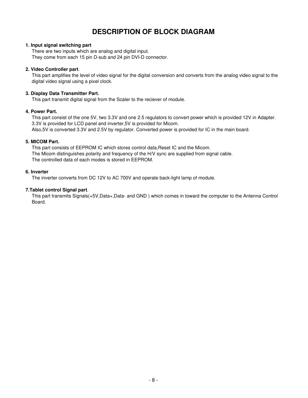
 "LG L1530TM液晶显示器维修手册和图纸-6")
 "LG L1530TM液晶显示器维修手册和图纸-7")
 "LG L1530TM液晶显示器维修手册和图纸-8")
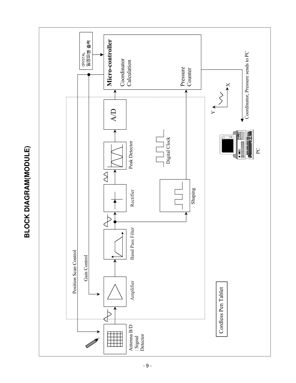 "LG L1530TM液晶显示器维修手册和图纸-9")
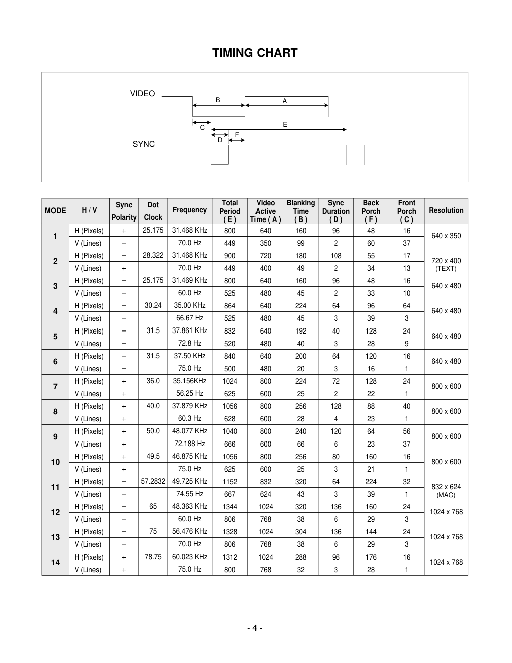
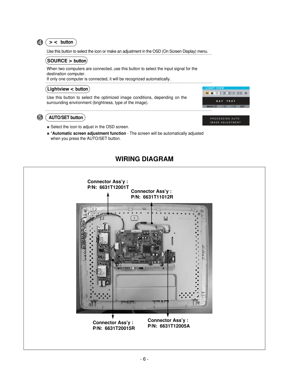
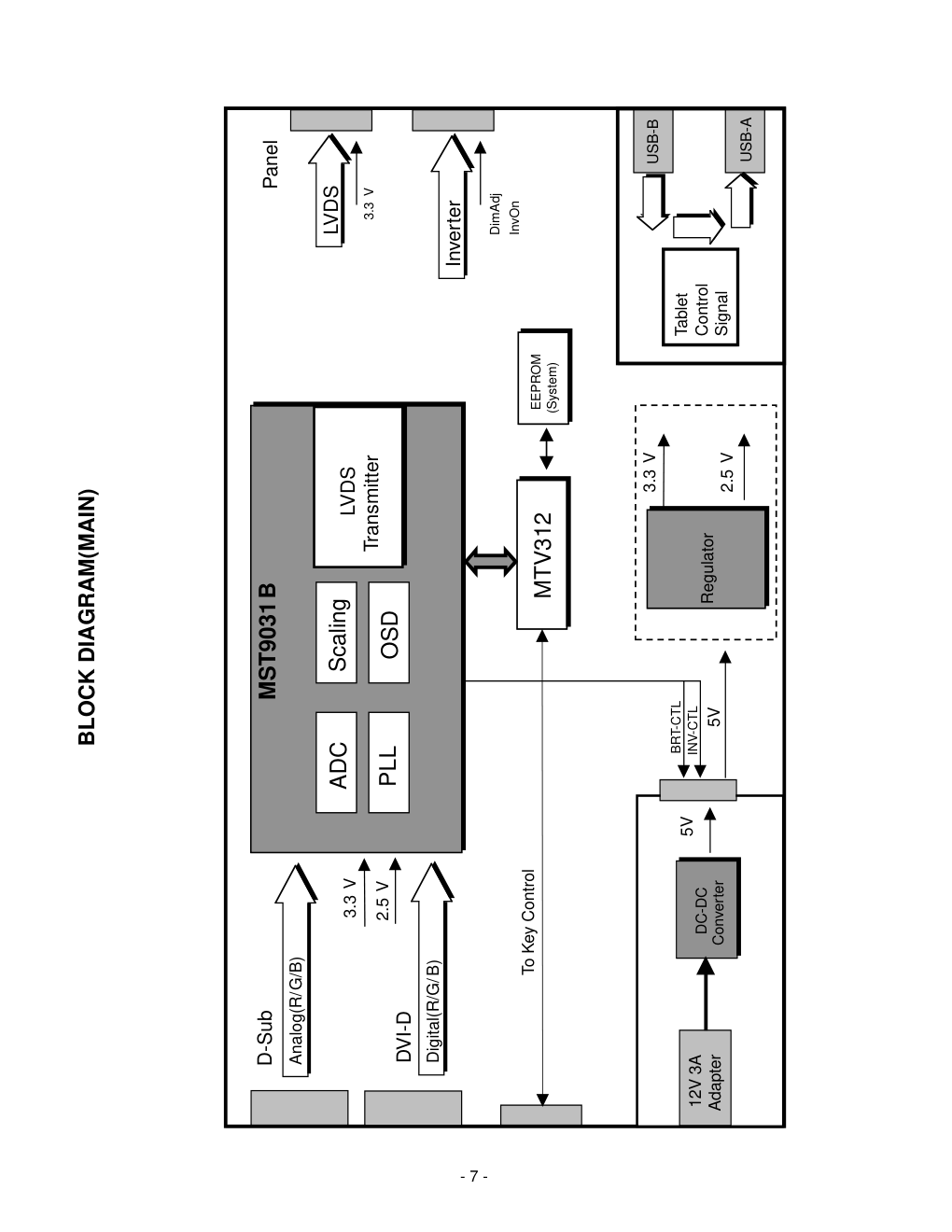
COLOR MONITOR SERVICE MANUAL Website:http://biz.LGservice.com E-mail:http://www.LGEservice.com/techsup.html CAUTION BEFORE SERVICING THE UNIT, READ THE SAFETY PRECAUTIONS IN THIS MANUAL. CHASSIS NO. : CL-61 MODEL: L1530TM (L1530TMM-AD**R) ( ) **Same model for Service - 1 - 1. LCD CHARACTERISTICS Type : TFT XGA LCD Module Pixel Pitch : 0.297mm x 0.297mm Color Depth : 6bits(with 2bit FRC)/ 16M colors Active Video Area : 15.0inch (304.128 x 228.096) Surface Treatment : Anti-Glare Backlight Unit : 4CCFL Opraating Mode : Normally white Electrical Interface : LVDS interface 2. OPTICAL CHARACTERISTICS 2-1. Viewing Angle by Contrast Ratio ≥ 10 Left : 80° min. 80° typ. Right: 80° min. 80° typ. Top : 80° min. 80° typ. Bottom: 80° min. 80° typ. 2-2. Luminance : 200(min.), 250(typ.) at Center point 2-3. Contrast Ratio : 300(min.), 400(typ.) 3. SIGNAL (Refer to the Timing Chart) 3-1. Sync Signal 1) Type : Separate Sync. (Horizontal & Vertical), SOG(Sync On Green), Digital, Composite 2) Input Voltage Level : Low=0~0.8V, High=2.1~5.5V 3) Sync Polarity : Positive or Negative 3-2. Video Input Signal 1) Type : R, G, B Analog 2) Voltage Level : 0~0.7 V 3) Input Impedance : 75 Ω 3-3. Operating Frequency Horizontal : 30 ~ 63kHz Vertical : 56 ~ 75Hz 4. POWER SUPPLY 4-1. Power 100-240V~, 50/60Hz DC 12V 3A 4-2. Power Consumption 5. ENVIRONMENT 5-1. Operating Temperature: 10°C~35°C (50°F~95°F) 5-2. Operating Humidity : 10%~80% 5-3. MTBF : 50,000 HRS (Min.) Lamp Life : 40,000 Hours (Min.) 6. DIMENSIONS (with TILT/SWIVEL) Width : 385.5mm (15.18'') Depth : 211.1mm (8.31'') Height : 354.5mm (13.96'') 7. WEIGHT (with TILT/SWIVEL) Net. Weight : 5.85kg (12.90 lbs) Gross Weight : 8.65kg (19.07 lbs) CONTENTS SPECIFICATIONS - 2 - SPECIFICATIONS ..................................................... 2 PRECAUTIONS ......................................................... 3 TIMING CHART ......................................................... 4 OPERATING INSTRUCTIONS .................................. 5 WIRING DIAGRAM .................................................... 6 BLOCK DIAGRAM ..................................................... 7 DESCRIPTION OF BLOCK DIAGRAM ..................... 8 BLOCK DIAGRAM(MODULE) ................................... 9 DESCRIPTION OF BLOCK DIAGRAM(MODULE) ..... 10 ADJUSTMENT ......................................................... 11 TROUBLESHOOTING GUIDE ................................ 13 EXPLODED VIEW.....................................................19 REPLACEMENT PARTS LIST .................................21 SCHEMATIC DIAGRAM........................................... 24 MODE POWER ON (NORMAL) STAND-BY SUSPEND DPM OFF POWER S/W OFF H/V SYNC ON/ON OFF/ON ON/OFF OFF - POWER CONSUMPTION less than 35 W less than 3 W less than 3 W less than 3 W less than 3 W LED COLOR GREEN AMBER AMBER AMBER OFF VIDEO ACTIVE OFF OFF OFF - - 3 - WARNING FOR THE SAFETY-RELATED COMPONENT. • There are some special components used in LCD monitor that are important for safety. These parts are marked on the schematic diagram and the replacement parts list. It is essential that these critical parts should be replaced with the manufacturer’s specified parts to prevent electric shock, fire or other hazard. • Do not modify original design without obtaining written permission from manufacturer or you will void the original parts and labor guarantee. TAKE CARE DURING HANDLING THE LCD MODULE WITH BACKLIGHT UNIT. • Must mount the module using mounting holes arranged in four corners. • Do not press on the panel, edge of the frame strongly or electric shock as this will result in damage to the screen. • Do not scratch or press on the panel with any sharp objects, such as pencil or pen as this may result in damage to the panel. • Protect the module from the ESD as it may damage the electronic circuit (C-MOS). • Make certain that treatment person’s body are grounded through wrist band. • Do not leave the module in high temperature and in areas of high humidity for a long time. • The module not be exposed to the direct sunlight. • Avoid contact with water as it may a short circuit within the module. • If the surface of panel become dirty, please wipe it off with a softmaterial. (Cleaning with a dirty or rough cloth may damage the panel.) WARNING BE CAREFUL ELECTRIC SHOCK ! • If you want to replace with the new backlight (CCFL) or inverter circuit, must disconnect the AC adapter because high voltage appears at inverter circuit about 650Vrms. • Handle with care wires or connectors of the inverter circuit. If the wires are pressed cause short and may burn or take fire. PRECAUTION CAUTION Please use only a plastic screwdriver to protect yourself from shock hazard during service operation. TIMING CHART - 4 - VIDEO SYNC B D C F E A H / V H (Pixels) V (Lines) H (Pixels) V (Lines) H (Pixels) V (Lines) H (Pixels) V (Lines) H (Pixels) V (Lines) H (Pixels) V (Lines) H (Pixels) V (Lines) H (Pixels) V (Lines) H (Pixels) V (Lines) H (Pixels) V (Lines) H (Pixels) V (Lines) H (Pixels) V (Lines) H (Pixels) V (Lines) H (Pixels) V (Lines) Sync Polarity + – – + – – – – – – – – + + + + + + + + – – – – – – + + Dot Clock 25.175 28.322 25.175 30.24 31.5 31.5 36.0 40.0 50.0 49.5 57.2832 65 75 78.75 Frequency 31.468 KHz 70.0 Hz 31.468 KHz 70.0 Hz 31.469 KHz 60.0 Hz 35.00 KHz 66.67 Hz 37.861 KHz 72.8 Hz 37.50 KHz 75.0 Hz 35.156KHz 56.25 Hz 37.879 KHz 60.3 Hz 48.077 KHz 72.188 Hz 46.875 KHz 75.0 Hz 49.725 KHz 74.55 Hz 48.363 KHz 60.0 Hz 56.476 KHz 70.0 Hz 60.023 KHz 75.0 Hz Resolution 640 x 350 720 x 400 640 x 480 640 x 480 640 x 480 640 x 480 800 x 600 800 x 600 800 x 600 800 x 600 832 x 624 1024 x 768 1024 x 768 1024 x 768 Total Period ( E ) 800 449 900 449 800 525 864 525 832 520 840 500 1024 625 1056 628 1040 666 1056 625 1152 667 1344 806 1328 806 1312 800 Video Active Time ( A ) 640 350 720 400 640 480 640 480 640 480 640 480 800 600 800 600 800 600 800 600 832 624 1024 768 1024 768 1024 768 Blanking Time ( B ) 160 99 180 49 160 45 224 45 192 40 200 20 224 25 256 28 240 66 256 25 320 43 320 38 304 38 288 32 Sync Duration ( D ) 96 2 108 2 96 2 64 3 40 3 64 3 72 2 128 4 120 6 80 3 64 3 136 6 136 6 96 3 Back Porch ( F ) 48 60 55 34 48 33 96 39 128 28 120 16 128 22 88 23 64 23 160 21 224 39 160 29 144 29 176 28 Front Porch ( C ) 16 37 17 13 16 10 64 3 24 9 16 1 24 1 40 1 56 37 16 1 32 1 24 3 24 3 16 1 MODE 1 2 3 4 5 6 7 8 9 10 11 12 13 14 (MAC) (TEXT) OPERATING INSTRUCTIONS - 5 - REAR VIEW Screen at the front side of the monitor D-Sub D-Sub DVI Power Cord USB FRONT VIEW Front Control Panel Screen at the front side of the monitor Buttons at the rear side of the monitor A green LED will be displayed in a normal operation mode, or an orange LED will be displayed in a power saving mode. Press the POWER button to turn the power on. Press the button again Shows or hides the OSD (On Screen Display) menu. Lock/Unlock OSD – Locks or unlocks the OSD adjustment function. To lock the OSD menu, press the MENU button for 5 seconds. The “OSD Locked” message will be displayed and the screen will be locked. To release OSD menu locking, press the MENU button for 5 seconds again. The “OSD Unlocked” message will appear and the OSD menu will be unlocked. OSD Locked OSD Unlocked MENU/EXIT button Power LED Power button - 6 - WIRING DIAGRAM Use this button to select the icon or make an adjustment in the OSD (On Screen Display) menu. When two computers are connected, use this button to select the input signal for the destination computer. If only one computer is connected, it will be recognized automatically. Use this button to select the optimized image conditions, depending on the surrounding environment (brightness, type of the image). Select the icon to adjust in the OSD screen. *Automatic screen adjustment function - The screen will be automatically adjusted when you press the AUTO/SET button. > < button AUTO/SET button Lightview < button L I G H T V I E W D A Y T E X T 1 2 MENU - + SET SOURCE > button Connector Ass’y : P/N: 6631T12001T Connector Ass’y : P/N: 6631T20015R Connector Ass’y : P/N: 6631T12005A Connector Ass’y : P/N: 6631T11012R - 7 - 5V 5V BRT-CTL INV-CTL MST9031B ADC Scaling PLL OSD LVDS Transmitter Panel MTV312 EEPROM (System) LVDS Analog(R/G/B) D-Sub To Key Control 3.3 V 3.3 V 2.5 V Regulator 3.3 V 2.5 V Digital(R/G/B) DVI-D DC-DC Converter 12V 3A Adapter Inverter DimAdj InvOn USB-B Tablet Control Signal USB-A BLOCK DIAGRAM(MAIN) - 8 - DESCRIPTION OF BLOCK DIAGRAM 1. Input signal switching part There are two inputs which are analog and digital input. They come from each 15 pin D-sub and 24 pin DVI-D connector. 2. Video Controller part. This part amplifies the level of video signal for the digital conversion and converts from the analog video signal to the digital video signal using a pixel clock. 3. Display Data Transmitter Part. This part transmit digital signal from the Scaler to the reciever of module. 4. Power Part. This part consist of the one 5V, two 3.3V and one 2.5 regulators to convert power which is provided 12V in Adapter. 3.3V is provided for LCD panel and inverter,5V is provided for Micom. Also,5V is converted 3.3V and 2.5V by regulator. Converted power is provided for IC in the main board. 5. MICOM Part. This part consists of EEPROM IC which stores control data,Reset IC and the Micom. The Micom distinguishes polarity and frequency of the H/V sync are supplied from signal cable. The controlled data of each modes is stored in EEPROM. 6. Inverter The inverter converts from DC 12V to AC 700V and operate back-light lamp of module. 7.Tablet control Signal part. This part transmits Signals(+5V,Data+,Data- and GND ) which comes in toward the computer to the Antenna Control Board. - 9 - BLOCK DIAGRAM(MODULE) - 10 - DESCRIPTION OF BLOCK DIAGRAM(MODULE) Detects the RF signal of the pen. Amplifies the detected RF signal to the level required for post processing. Filters the signal outside of the necessary RF bandwidth. Rectifies the abandoned boltage. Finds the most intensive signal among the signals detected by the antenna. Makes the signal detected by the peak detector as a quantum. Detects the pressure level by converting the sine wave type signal to that of the digital clock. Figures out location and pressure value using the input signals. - 11 - ADJUSTMENT Windows EDID V1.0 User Manual Operating System: MS Windows 98, 2000, XP Port Setup: Windows 98 => Don’t need setup Windows 2000, XP => Need to Port Setup. This program is available to LCD Monitor only. 1. Port Setup a) Copy “UserPort.sys” file to “c:\WINNT\system32\drivers” folder b) Run Userport.exe c) Remove all default number d) Add 300-3FF e) Click Start button. f) Click Exit button. 2. EDID Read & Write 1) Run WinEDID.exe 2) Edit Week of Manufacture, Year of Manufacture, Serial Number a) Input User Info Data b) Click “Update” button c) Click “ Write” button - 12 - Figure 1. Cable Connection SERVICE OSD 1)Turn off the power switch at the front side of display. 2)Wait for about 5 seconds and press MENU,POWER key with 1 second interval. 3)Shows the service OSD menu. 4)The service OSD menu contains additional menus that the User OSD menu as described below. a)CLEAR ETI : To initialize using time. b)AUTO COLOR : W/B balance and Automatically sets the gain and offset value. c)AGING :Select Aging mode on/off.(default :off) d)PANEL : Shows the panel name. e)NVRAM INIT : EEPROM initialize(24C16). f)9300 : Allows you to set the R/G/B.-9300K value manually. g)6500 :Allows you to set the R/G/B.-6500K value manually. h)OFFSET : Allows you to set the R/G/B.-Offset value manually.(Analog Only) i)GAIN : Allows you to set the R/G/B.-Gain value manually.(Analog Only) - 13 - TROUBLESHOOTING GUIDE 1. NO POWER NO POWER (POWER INDICATOR OFF) CHECK ADAPTER, AND FIND OUT SHORT POINT OF EACH DC LINE OF 2.5V AND 3.3V CHECK J801'S VOLTAGE (12V)? NO CHECK X501. CHECK X501'S WAVEFORM OSCILLATE AS 12MHZ? CHECK U806 PIN 5, 6 WAVEERFORM? NO CHECK U806 AND L803 NO YES YES CHECK KEY CONTROL CONNECTOR ROUTINE *J801: POWER JACK *X501: 12MHZ CRISTAL *U806: L4978D(REGULATOR) *L803: COIL - 14 - 2. NO RASTER (OSD IS NOT DISPLAYED) – LIPS CHECK MICOM INV ON/OFF PORT. J706 PIN4 5V? NO NO RASTER (OSD IS NOT DISPLAYED) CHECK ADAPTER J706 PIN 7,8 PIN 12V? NO 1.CONFIRM BRIGHTNESS OSD CONTROL STATE. 2.CHECK MICOM DIM-ADJ PORT J706 PIN1 5V? NO REPLACE INVERTER ASS'Y CHECK PULSE AS CONTACTING SCOPTE PROBE TO CAUTIN LABEL. (CONTACT PROBE TO CAUTIN LABEL.) CAN YOU SEE PULSE AT YOUR SCOPE? NO REPLACE CCFL LAMP IN THE LCD MODULE YES YES YES YES *J706: 8P Wafer for Inverter - 15 - CHECK U201 SOLDERING CONDITION AND CHECK CONNECTION LINE FROM U201 TO U501. U801,U802,U803 POWER PINS 3.3V,2.5V NO CHECK U801,U802, U803 INPUT 1024*768@60Hz Signal. U201 PIN126 IS 48KHz H-SYNC? PIN127 IS 60Hz V-SYNC? AT SIGNAL PINS? CHECK U801 TROUBLE IN CABLE OR LCD MODULE YES YES 3. WHITE SCREEN (OSD IS NOT DISPLAYED) – MST9031B WHITE SCREEN (OSD IS NOT DISPLAYED) J704'S PIN1 3.3V? NO NO YES *U801, U802, U803: Regulator *U201: MST9031B(LCD Controller) *U501: MICOM(MTV312MV64) *J704: 20P Wafer - 16 - 4. TROUBLE IN DPM TROUBLE IN DPM TROUBLE IN U501 CHECK PC PC IS NOT GOING INTO DPM OFF MODE NO CHECK H/V SYNC LINE NO YES YES CHECK R773, R775 (SYNC) ? CHECK U501 PIN 43.44 SYNC PULSE ? - 17 - TROUBLESHOOTING GUIDE(TABLET) 1. IF THE MOUSE POINTER DOES NOT MOVE The mouse pointer is not moving. Check voltage (+/-5V) of U701 and J707 in the main board. +/-5V Voltage from the USB jack should be transferred to the digitizer control board. Did you check JP1 voltage(+/-5V)? Can you see a Tablet Manager icon on the Task Bar? NO Reconnect FFC cable. Check the connection between the digitizer control board and the antenna board (P1, P2 and P3) NO Replace the digitizer control board. NO YES YES Replace the digitizer control board. YES Dose thepen work normally? Replace the pen. NO YES *JP1 : Wafer on the digitizer control board. *P1, P2 and P3: Wafer between the digitizer board and the antenna board(P1, P2 and P3) - 18 - 2. THE MOUSE POINTER DOES NOT MOVE PROPERLY The mouse pointer does not move along with the pen(excluding corner areas). Reconnect the FFC cable. Check whether the digitizer control board is properly connectde to the antenna board (P1, P2 and P3) Does the tablet pen work normally? NO Replace the antenna board. The mouse pointer jumps to another position in the screen display area. NO Replace the pen. NO YES YES Replace the digiizer control board. YES - 19 - EXPLODED VIEW - 20 - EXPLODED VIEW PARTS LIST 1 2 3 4 5 6 7 8 9 10 11 12 13 14 15 16 17 18 19 20 21 22 23 24 25 3091TKL101A CABINET ASSEMBLY, L1530TMM BRAND 3090TKL092A 6304FBH006A LCD(LIQUID CRYSTAL DISPLAY), HT15X23-100 BOE-HYDIS TFT COLOR XGA LVDS 280NITS FFS 40MS X6 CD_3.02 6304FBH006B LCD(LIQUID CRYSTAL DISPLAY), HT15X23-100 BOE-HYDIS TFT COLOR XGA LVDS 280NITS FFS 40MS X7 CD_3.03 - For USA / CANADA 3809TKL072A BACK COVER ASSEMBLY, L1530TMM 3808TKL075A INNER 3043TKK152A TILT SWIVEL ASSEMBLY, L1530TMM BRAND(TABLET) 3043TKK159A TILT SWIVEL ASSEMBLY, LB500 . LB500 WA#4 NEW LG LOGO REAR COVER - For USA / CANADA 3790T15002A WINDOW, ASAHI GLASS 15'' L1530TMM(TABLET) 6871TST471A "PWB(PCB) ASSEMBLY,SUB", L1530TMM CONTROL TOTAL BRAND 5040TKM065A RUBBER, SUPPORT MOLDING L1530TMM 4950TKS269A METAL, FRAME MAIN(L1530TMM) 6633TZA008L INVERTER ASSEMBLY, "ALPS KUBNKM078A L1530TMM,4-LAMPS TABLET" 3313TL5080B MAIN TOTAL ASSEMBLY, L1530TMM BRAND CL-32 4950TKK737A METAL, FIX SIGNAL(L1530TMM) 4950TKK750A METAL, SHIELD REAR-L1530TMM 5040TKM069A RUBBER, SUPPORT MOLDING ,L1530TMM 3809TKL073A BACK COVER ASSEMBLY, L1530TMM 3808TKL076A OUTER 4950TKK742A METAL, FIX DIE-CASTING(L1530TMM) 4940TKK051A KNOB, STAND FIX(L1530TMM) 4950TKK738A METAL, BACK PLATE (L1530TMM) 3551TKK506A COVER ASSEMBLY, L1530TMM REAR 3550TKK488A DOOR 6871TKE001A PWB(PCB) ASSEMBLY,INTERFACE, L1530TMM ETC TOTAL BRAND PEN ASSY 3551TKK507A COVER ASSEMBLY, L1530TMM TOTAL PEN HOLDER 6850TD9004G CABLE,D-SUB, UL20276-9C(5.8MM) DT 1800MM BLACK(9930) SONY DM 6866TDV004Q CABLE,DVI, UL20276 AWG30 DT 1800MM BLACK(9930) HX73 DM 6866TDU002A CABLE,D-SUB, UL20276 DT 1870MM BLACK LQ800 DM 6410TEW003A POWER CORD, SP023+IS14 I-SHENG VDE/SEMKO 1870MM WALL BLACK 6410TUW003B POWER CORD, PS204+V1625 VOLEX UL/CSA 1800MM WALL BLACK- For USA / CANADA 6410TBW001B POWER CORD,SP60+IS14 I-SHENG BSI 1870MM WALL BLACK - For Singapore 6634B00046A ADAPTER,AC-DC, LSE0107A1236 LISHIN 12V 3.0A FOR LG Description Part No. Ref. No. - 21 - DATE: 2004. 5. 11. *S *AL LOC. NO. PART NO. DESCRIPTION / SPECIFICATION C204 0CK103CK51A 0.01UF 1608 50V 10% R/TP B(Y5 C205 0CK103CK51A 0.01UF 1608 50V 10% R/TP B(Y5 C206 0CK103CK51A 0.01UF 1608 50V 10% R/TP B(Y5 C207 0CK104CK56A 0.1UF 1608 50V 10% R/TP X7R C208 0CK104CK56A 0.1UF 1608 50V 10% R/TP X7R C209 0CK104CK56A 0.1UF 1608 50V 10% R/TP X7R C210 0CK104CK56A 0.1UF 1608 50V 10% R/TP X7R C211 0CK104CK56A 0.1UF 1608 50V 10% R/TP X7R C213 0CK104CK56A 0.1UF 1608 50V 10% R/TP X7R C214 0CK104CK56A 0.1UF 1608 50V 10% R/TP X7R C215 0CK104CK56A 0.1UF 1608 50V 10% R/TP X7R C216 0CK104CK56A 0.1UF 1608 50V 10% R/TP X7R C217 0CK104CK56A 0.1UF 1608 50V 10% R/TP X7R C218 0CK104CK56A 0.1UF 1608 50V 10% R/TP X7R C219 0CK104CK56A 0.1UF 1608 50V 10% R/TP X7R C220 0CK104CK56A 0.1UF 1608 50V 10% R/TP X7R C221 0CK104CK56A 0.1UF 1608 50V 10% R/TP X7R C222 0CK104CK56A 0.1UF 1608 50V 10% R/TP X7R C223 0CK104CK56A 0.1UF 1608 50V 10% R/TP X7R C224 0CK104CK56A 0.1UF 1608 50V 10% R/TP X7R C225 0CK104CK56A 0.1UF 1608 50V 10% R/TP X7R C226 0CK104CK56A 0.1UF 1608 50V 10% R/TP X7R C227 0CK104CK56A 0.1UF 1608 50V 10% R/TP X7R C230 0CK104CK56A 0.1UF 1608 50V 10% R/TP X7R C231 0CK103CK51A 0.01UF 1608 50V 10% R/TP B(Y5 C232 0CK103CK51A 0.01UF 1608 50V 10% R/TP B(Y5 C233 0CK103CK51A 0.01UF 1608 50V 10% R/TP B(Y5 C240 0CK103CK51A 0.01UF 1608 50V 10% R/TP B(Y5 C500 0CK104CK56A 0.1UF 1608 50V 10% R/TP X7R C501 0CH8106F691 10UF 16V 20% 105STD (CYL) R/T C502 0CC101CK41A 100PF 1608 50V 5% R/TP NP0 C503 0CC101CK41A 100PF 1608 50V 5% R/TP NP0 C505 0CC101CK41A 100PF 1608 50V 5% R/TP NP0 C506 0CC101CK41A 100PF 1608 50V 5% R/TP NP0 C507 0CH8106F691 10UF 16V 20% 105STD (CYL) R/T C512 0CC180CK41A 18PF 1608 50V 5% R/TP NP0 C513 0CC100CK41A 10PF 1608 50V 5% R/TP NP0 C516 0CK104CK56A 0.1UF 1608 50V 10% R/TP X7R C703 0CK104CK56A 0.1UF 1608 50V 10% R/TP X7R C707 0CC680CK41A 68PF 1608 50V 5% R/TP NP0 C708 0CK103CK51A 0.01UF 1608 50V 10% R/TP B(Y5 C709 0CK103CK51A 0.01UF 1608 50V 10% R/TP B(Y5 C710 0CK103CK51A 0.01UF 1608 50V 10% R/TP B(Y5 C711 0CK103CK51A 0.01UF 1608 50V 10% R/TP B(Y5 C712 0CK104CK56A 0.1UF 1608 50V 10% R/TP X7R C713 0CC101CK41A 100PF 1608 50V 5% R/TP NP0 C714 0CC101CK41A 100PF 1608 50V 5% R/TP NP0 C727 0CK105CD56A 1UF 1608 10V 10% R/TP X7R C730 0CC101CK41A 100PF 1608 50V 5% R/TP NP0 C731 0CC680CK41A 68PF 1608 50V 5% R/TP NP0 C732 0CK103CK51A 0.01UF 1608 50V 10% R/TP B(Y5 C733 0CK104CK56A 0.1UF 1608 50V 10% R/TP X7R DATE: 2004. 5. 11. *S *AL LOC. NO. PART NO. DESCRIPTION / SPECIFICATION C734 0CK104CK56A 0.1UF 1608 50V 10% R/TP X7R C735 0CK104CK56A 0.1UF 1608 50V 10% R/TP X7R C737 0CK104CK56A 0.1UF 1608 50V 10% R/TP X7R C738 0CK104CK56A 0.1UF 1608 50V 10% R/TP X7R C739 0CK104CK56A 0.1UF 1608 50V 10% R/TP X7R C740 0CK104CK56A 0.1UF 1608 50V 10% R/TP X7R C744 0CK104CK56A 0.1UF 1608 50V 10% R/TP X7R C745 0CK104CK56A 0.1UF 1608 50V 10% R/TP X7R C746 0CK104CK56A 0.1UF 1608 50V 10% R/TP X7R C747 0CK104CK56A 0.1UF 1608 50V 10% R/TP X7R C750 0CK104CK56A 0.1UF 1608 50V 10% R/TP X7R C801 0CK103CK51A 0.01UF 1608 50V 10% R/TP B(Y5 C802 0CK104CK56A 0.1UF 1608 50V 10% R/TP X7R C803 0CK104CK56A 0.1UF 1608 50V 10% R/TP X7R C807 0CE477EF610 "470UF KMG,RD 16V 20% BULK FL" C817 0CE477ED610 "470UF KMG,RD 10V 20% FL BULK" C818 0CK104CK56A 0.1UF 1608 50V 10% R/TP X7R C819 0CK103CK51A 0.01UF 1608 50V 10% R/TP B(Y5 C820 0CZZTAT005B RJ4-16V101MX ELNA 16V 100UF 2 C821 0CK103CK51A 0.01UF 1608 50V 10% R/TP B(Y5 C822 0CK104CK56A 0.1UF 1608 50V 10% R/TP X7R C828 0CK104CK56A 0.1UF 1608 50V 10% R/TP X7R C829 0CK103CK51A 0.01UF 1608 50V 10% R/TP B(Y5 C831 0CZZTAT005B RJ4-16V101MX ELNA 16V 100UF 2 C832 0CZZTAT005B RJ4-16V101MX ELNA 16V 100UF 2 C833 0CC221CK41A 220PF 1608 50V 5% R/TP NP0 C834 0CK104CK56A 0.1UF 1608 50V 10% R/TP X7R C835 0CC221CK41A 220PF 1608 50V 5% R/TP NP0 C836 0CK104CK56A 0.1UF 1608 50V 10% R/TP X7R C837 0CE477EF610 "470UF KMG,RD 16V 20% BULK FL" C838 0CK104CK56A 0.1UF 1608 50V 10% R/TP X7R C839 0CK104CK56A 0.1UF 1608 50V 10% R/TP X7R C840 0CK104CK56A 0.1UF 1608 50V 10% R/TP X7R C841 0CK223CK51A 0.022UF 1608 50V 10% R/TP B(Y C842 0CK152CK51A 1500PF 1608 50V 10% R/TP B(Y5 C843 0CK104CK56A 0.1UF 1608 50V 10% R/TP X7R C844 0CE477EF610 "470UF KMG,RD 16V 20% BULK FL" C845 0CK103CK51A 0.01UF 1608 50V 10% R/TP B(Y5 C846 0CK103CK51A 0.01UF 1608 50V 10% R/TP B(Y5 D701 0DS226009AA KDS226 TP KEC SOT-23 80V 300 D702 0DS226009AA KDS226 TP KEC SOT-23 80V 300 D703 0DS226009AA KDS226 TP KEC SOT-23 80V 300 D704 0DS226009AA KDS226 TP KEC SOT-23 80V 300 D706 0DS226009AA KDS226 TP KEC SOT-23 80V 300 D707 0DD184009AA KDS184 TP KEC - 85V - - - 300 D708 0DS226009AA KDS226 TP KEC SOT-23 80V 300 D709 0DS226009AA KDS226 TP KEC SOT-23 80V 300 D710 0DS226009AA KDS226 TP KEC SOT-23 80V 300 D711 0DS226009AA KDS226 TP KEC SOT-23 80V 300 D712 0DS226009AA KDS226 TP KEC SOT-23 80V 300 D713 0DS226009AA KDS226 TP KEC SOT-23 80V 300 REPLACEMENT PARTS LIST CAUTION: BEFORE REPLACING ANY OF THESE COMPONENTS, READ CAREFULLY THE SAFETY PRECAUTIONS IN THIS MANUAL. * NOTE : S SAFETY Mark AL ALTERNATIVE PARTS MAIN BOARD CAPACITORS DIODEs DATE: 2004. 5. 11. *S *AL LOC. NO. PART NO. DESCRIPTION / SPECIFICATION D714 0DS226009AA KDS226 TP KEC SOT-23 80V 300 D715 0DS226009AA KDS226 TP KEC SOT-23 80V 300 D716 0DS226009AA KDS226 TP KEC SOT-23 80V 300 D717 0DS226009AA KDS226 TP KEC SOT-23 80V 300 D718 0DS226009AA KDS226 TP KEC SOT-23 80V 300 D719 0DD184009AA KDS184 TP KEC - 85V - - - 300 D720 0DS226009AA KDS226 TP KEC SOT-23 80V 300 D721 0DS226009AA KDS226 TP KEC SOT-23 80V 300 D722 0DS226009AA KDS226 TP KEC SOT-23 80V 300 ZD701 0DZ560009GB BZT52C5V6S DIODES R/TP SOD323 ZD702 0DZ560009GB BZT52C5V6S DIODES R/TP SOD323 ZD703 0DZ560009GB BZT52C5V6S DIODES R/TP SOD323 ZD704 0DZ560009GB BZT52C5V6S DIODES R/TP SOD323 ZD705 0DZ560009GB BZT52C5V6S DIODES R/TP SOD323 ZD706 0DZ560009GB BZT52C5V6S DIODES R/TP SOD323 ZD708 0DZ560009DA UDZ S 5.6B TP ROHM-K SOD323 2 ZD709 0DZ560009GB BZT52C5V6S DIODES R/TP SOD323 ZD710 0DZ560009DA UDZ S 5.6B TP ROHM-K SOD323 2 ZD711 0DZ560009GB BZT52C5V6S DIODES R/TP SOD323 ZD712 0DZ560009GB BZT52C5V6S DIODES R/TP SOD323 ZD713 0DZ560009DA UDZ S 5.6B TP ROHM-K SOD323 2 ZD715 0DZ560009GB BZT52C5V6S DIODES R/TP SOD323 ZD716 0DZ560009GB BZT52C5V6S DIODES R/TP SOD323 ZD801 0DRSG00028A STPS340U SGS-THOMSON R/TP SMB U201 0IPRPM3009B "MST9031B(DUAL) MSTAR 128P,LQF" U501 0IZZTSZ324B MYSON 44P L1530TMM E U502 0IMMRSS040C S524A60X51(SCT0) SAMSUNG ELEC U701 6630SK00804 "UAR24-4K2300 ACON 4P 2.0MM ""B" U702 0ICS240213A CAT24W(F)C02J-TE13 8P SOP TP U703 0ICS240213A CAT24W(F)C02J-TE13 8P SOP TP U801 0IPMGNS001E LM1117MPX-3.3 NATIONAL SEMICO U802 0IRH033000A BA033SFP P/MOLD-5 TP REGULATO U803 0IPMGNS001D LM1117MPX-2.5 NATIONAL SEMICO U805 0TFFC80009A FAIRCHILD FDC6326L R/TP SOT-6 U806 0IPMGSG008A "L4978D SGS-THOMSON 16P,SOIC R" U807 0TFVI80023A VISHAY SI3865DV R/TP TSOP-6 8 L701 6210TCE001S HU-1M2012-121 CERATECH 2012MM L801 6210TCE001G HH-1M3216-501 CERATEC 3216MM L803 6140TBZ016E "LX31 GET DR10*7,0.45*37TS,68U" L805 6210TCE001C HB-1T3216-500JT CERATEC 3216M L806 6210TCE001S HU-1M2012-121 CERATECH 2012MM Q502 0TR390409AE FAIRCHILD KST3904(LGEMTF) TP Q503 0IKE704200H KIA7042AP TO-92 TP 4.2 VOLT. Q505 0TR390409AE FAIRCHILD KST3904(LGEMTF) TP Q506 0TR390409AE FAIRCHILD KST3904(LGEMTF) TP Q701 0TR390409AE FAIRCHILD KST3904(LGEMTF) TP Q702 0TR390409AE FAIRCHILD KST3904(LGEMTF) TP Q703 0TR390609FA KST3906-MTF TP SAMSUNG SOT23 Q704 0TR390609FA KST3906-MTF TP SAMSUNG SOT23 R201 0RJ1500D677 150 OHM 1/10 W 5% 1608 R/TP DATE: 2004. 5. 11. *S *AL LOC. NO. PART NO. DESCRIPTION / SPECIFICATION R202 0RJ1500D677 150 OHM 1/10 W 5% 1608 R/TP R203 0RJ1500D677 150 OHM 1/10 W 5% 1608 R/TP R204 0RJ0000D677 0 OHM 1/10 W 5% 1608 R/TP R207 0RJ3900D677 390 OHM 1/10 W 5% 1608 R/TP R208 0RJ1500D677 150 OHM 1/10 W 5% 1608 R/TP R209 0RJ1500D677 150 OHM 1/10 W 5% 1608 R/TP R210 0RJ1500D677 150 OHM 1/10 W 5% 1608 R/TP R220 0RJ4701D677 4.7K OHM 1/10 W 5% 1608 R/TP R240 0RJ1500D677 150 OHM 1/10 W 5% 1608 R/TP R501 0RJ4701D677 4.7K OHM 1/10 W 5% 1608 R/TP R502 0RJ4701D677 4.7K OHM 1/10 W 5% 1608 R/TP R503 0RJ4701D677 4.7K OHM 1/10 W 5% 1608 R/TP R504 0RJ4701D677 4.7K OHM 1/10 W 5% 1608 R/TP R505 0RJ4701D677 4.7K OHM 1/10 W 5% 1608 R/TP R507 0RJ4701D677 4.7K OHM 1/10 W 5% 1608 R/TP R508 0RJ4701D677 4.7K OHM 1/10 W 5% 1608 R/TP R509 0RJ4701D677 4.7K OHM 1/10 W 5% 1608 R/TP R510 0RJ4701D677 4.7K OHM 1/10 W 5% 1608 R/TP R511 0RJ4701D677 4.7K OHM 1/10 W 5% 1608 R/TP R512 0RJ2001D677 2K OHM 1/10 W 5% 1608 R/TP R514 0RJ1002D677 10K OHM 1/10 W 5% 1608 R/TP R517 0RJ1000D677 100 OHM 1/10 W 5% 1608 R/TP R519 0RJ1000D677 100 OHM 1/10 W 5% 1608 R/TP R520 0RJ1000D677 100 OHM 1/10 W 5% 1608 R/TP R521 0RJ1000D677 100 OHM 1/10 W 5% 1608 R/TP R522 0RJ1000D677 100 OHM 1/10 W 5% 1608 R/TP R523 0RJ1000D677 100 OHM 1/10 W 5% 1608 R/TP R524 0RJ1000D677 100 OHM 1/10 W 5% 1608 R/TP R525 0RJ1000D677 100 OHM 1/10 W 5% 1608 R/TP R526 0RJ1000D677 100 OHM 1/10 W 5% 1608 R/TP R527 0RJ1000D677 100 OHM 1/10 W 5% 1608 R/TP R532 0RJ3301D677 3.3K OHM 1/10 W 5% 1608 R/TP R533 0RJ0332D677 33 OHM 1/10 W 5% 1608 R/TP R534 0RJ0332D677 33 OHM 1/10 W 5% 1608 R/TP R535 0RJ3301D677 3.3K OHM 1/10 W 5% 1608 R/TP R537 0RJ4701D677 4.7K OHM 1/10 W 5% 1608 R/TP R541 0RJ4701D677 4.7K OHM 1/10 W 5% 1608 R/TP R544 0RJ4700D677 470 OHM 1/10 W 5% 1608 R/TP R545 0RJ4700D677 470 OHM 1/10 W 5% 1608 R/TP R570 0RJ4701D677 4.7K OHM 1/10 W 5% 1608 R/TP R571 0RJ4701D677 4.7K OHM 1/10 W 5% 1608 R/TP R572 0RJ4701D677 4.7K OHM 1/10 W 5% 1608 R/TP R573 0RJ4701D677 4.7K OHM 1/10 W 5% 1608 R/TP R574 0RJ4701D677 4.7K OHM 1/10 W 5% 1608 R/TP R575 0RJ4701D677 4.7K OHM 1/10 W 5% 1608 R/TP R576 0RJ1000D677 100 OHM 1/10 W 5% 1608 R/TP R577 0RJ1000D677 100 OHM 1/10 W 5% 1608 R/TP R582 0RJ1000D677 100 OHM 1/10 W 5% 1608 R/TP R584 0RJ4701D677 4.7K OHM 1/10 W 5% 1608 R/TP R585 0RJ0332D677 33 OHM 1/10 W 5% 1608 R/TP R586 0RJ0332D677 33 OHM 1/10 W 5% 1608 R/TP R587 0RJ2200D677 220 OHM 1/10 W 5% 1608 R/TP R588 0RJ1000D677 100 OHM 1/10 W 5% 1608 R/TP R589 0RJ1000D677 100 OHM 1/10 W 5% 1608 R/TP R590 0RJ1000D677 100 OHM 1/10 W 5% 1608 R/TP R591 0RJ1000D677 100 OHM 1/10 W 5% 1608 R/TP R592 0RJ4701D677 4.7K OHM 1/10 W 5% 1608 R/TP R593 0RJ1000D677 100 OHM 1/10 W 5% 1608 R/TP R594 0RJ1000D677 100 OHM 1/10 W 5% 1608 R/TP R595 0RJ1000D677 100 OHM 1/10 W 5% 1608 R/TP R701 0RJ0752D677 75 OHM 1/10 W 5% 1608 R/TP R702 0RJ4701D677 4.7K OHM 1/10 W 5% 1608 R/TP - 22 - RESISTORs ICs TRANSISTOR COIL & COREs DATE: 2004. 5. 11. *S *AL LOC. NO. PART NO. DESCRIPTION / SPECIFICATION R703 0RJ0752D677 75 OHM 1/10 W 5% 1608 R/TP R704 0RJ4701D677 4.7K OHM 1/10 W 5% 1608 R/TP R705 0RJ1000D677 100 OHM 1/10 W 5% 1608 R/TP R706 0RJ0752D677 75 OHM 1/10 W 5% 1608 R/TP R707 0RJ0272D677 27 OHM 1/10 W 5% 1608 R/TP R708 0RJ4700D677 470 OHM 1/10 W 5% 1608 R/TP R709 0RJ4700D677 470 OHM 1/10 W 5% 1608 R/TP R710 0RJ1000D677 100 OHM 1/10 W 5% 1608 R/TP R711 0RJ0000D677 0 OHM 1/10 W 5% 1608 R/TP R712 0RJ0000D677 0 OHM 1/10 W 5% 1608 R/TP R713 0RJ0000D677 0 OHM 1/10 W 5% 1608 R/TP R714 0RJ0000D677 0 OHM 1/10 W 5% 1608 R/TP R715 0RJ0000D677 0 OHM 1/10 W 5% 1608 R/TP R716 0RJ4701D677 4.7K OHM 1/10 W 5% 1608 R/TP R717 0RJ4701D677 4.7K OHM 1/10 W 5% 1608 R/TP R718 0RJ0000D677 0 OHM 1/10 W 5% 1608 R/TP R719 0RJ0000D677 0 OHM 1/10 W 5% 1608 R/TP R720 0RJ0000D677 0 OHM 1/10 W 5% 1608 R/TP R722 0RJ1000D677 100 OHM 1/10 W 5% 1608 R/TP R723 0RJ0332D677 33 OHM 1/10 W 5% 1608 R/TP R724 0RJ0332D677 33 OHM 1/10 W 5% 1608 R/TP R726 0RJ4701D677 4.7K OHM 1/10 W 5% 1608 R/TP R727 0RJ4701D677 4.7K OHM 1/10 W 5% 1608 R/TP R728 0RJ0222D677 22 OHM 1/10 W 5% 1608 R/TP R729 0RJ0222D677 22 OHM 1/10 W 5% 1608 R/TP R730 0RJ1000D677 100 OHM 1/10 W 5% 1608 R/TP R731 0RJ4700D677 470 OHM 1/10 W 5% 1608 R/TP R733 0RJ1001D677 1K OHM 1/10 W 5% 1608 R/TP R734 0RJ4701D677 4.7K OHM 1/10 W 5% 1608 R/TP R740 0RJ1001D677 1K OHM 1/10 W 5% 1608 R/TP R741 0RJ4701D677 4.7K OHM 1/10 W 5% 1608 R/TP R744 0RJ4701D677 4.7K OHM 1/10 W 5% 1608 R/TP R745 0RJ4701D677 4.7K OHM 1/10 W 5% 1608 R/TP R747 0RJ4701D677 4.7K OHM 1/10 W 5% 1608 R/TP R748 0RJ4701D677 4.7K OHM 1/10 W 5% 1608 R/TP R750 0RJ4700D677 470 OHM 1/10 W 5% 1608 R/TP R751 0RJ4701D677 4.7K OHM 1/10 W 5% 1608 R/TP R763 0RJ4701D677 4.7K OHM 1/10 W 5% 1608 R/TP R764 0RJ4701D677 4.7K OHM 1/10 W 5% 1608 R/TP R765 0RJ0332D677 33 OHM 1/10 W 5% 1608 R/TP R766 0RJ0332D677 33 OHM 1/10 W 5% 1608 R/TP R772 0RJ0222D677 22 OHM 1/10 W 5% 1608 R/TP R773 0RJ0222D677 22 OHM 1/10 W 5% 1608 R/TP R774 0RJ0222D677 22 OHM 1/10 W 5% 1608 R/TP R775 0RJ0222D677 22 OHM 1/10 W 5% 1608 R/TP R776 0RJ0222D677 22 OHM 1/10 W 5% 1608 R/TP R777 0RJ0222D677 22 OHM 1/10 W 5% 1608 R/TP R817 0RJ0000D677 0 OHM 1/10 W 5% 1608 R/TP R818 0RJ0000D677 0 OHM 1/10 W 5% 1608 R/TP R819 0RJ0000D677 0 OHM 1/10 W 5% 1608 R/TP R821 0RJ1001D677 1K OHM 1/10 W 5% 1608 R/TP R822 0RJ2202D677 22K OHM 1/10 W 5% 1608 R/TP R840 0RJ0102D677 10 OHM 1/10 W 5% 1608 R/TP R841 0RJ0102D677 10 OHM 1/10 W 5% 1608 R/TP R842 0RJ0102D677 10 OHM 1/10 W 5% 1608 R/TP R843 0RJ0102D677 10 OHM 1/10 W 5% 1608 R/TP R844 0RJ0102D677 10 OHM 1/10 W 5% 1608 R/TP R845 0RJ0102D677 10 OHM 1/10 W 5% 1608 R/TP R846 0RJ0102D677 10 OHM 1/10 W 5% 1608 R/TP R847 0RJ0102D677 10 OHM 1/10 W 5% 1608 R/TP R848 0RJ0102D677 10 OHM 1/10 W 5% 1608 R/TP R849 0RJ0102D677 10 OHM 1/10 W 5% 1608 R/TP DATE: 2004. 5. 11. *S *AL LOC. NO. PART NO. DESCRIPTION / SPECIFICATION R850 0RJ1003D677 100K OHM 1/10 W 5% 1608 R/TP R851 0RJ9101D677 9.1K OHM 1/10 W 5% 1608 R/TP R852 0RJ4701D677 4.7K OHM 1/10 W 5% 1608 R/TP R853 0RJ2701D677 2.7K OHM 1/10 W 5% 1608 R/TP R854 0RJ2002D677 20000 OHM 1/10 W 5% 1608 R/TP R855 0RJ1003D677 100K OHM 1/10 W 5% 1608 R/TP X501 6212AA2004A HC-49U TXC 12.0MHZ +/- 30 PPM LED1 0DLBE0028AA BRIGHT LED ELECTRONICS BL-HKB R1 0RH6800D622 680 OHM 1 / 10 W 5% D R/TP R2 0RH1201D622 1.2K 1/10W 5 D.R/TP R3 0RH2701D622 2.7K 1/10W 5 D.R/TP SW1 6600R00004A JTP1138A6EM JEIL 12VDC 50MA S SW2 6600R00004A JTP1138A6EM JEIL 12VDC 50MA S SW3 6600R00004A JTP1138A6EM JEIL 12VDC 50MA S SW4 6600R00004A JTP1138A6EM JEIL 12VDC 50MA S SW5 6600R00004A JTP1138A6EM JEIL 12VDC 50MA S - 23 - OTHERs CONTROL BOARD SCHEMATIC DIAGRAM - 24 - 1. SCALER - 25 - 2. MICOM - 26 - 3. POWER - 27 - 4. CONNECTOR & JACKS / 8 Blank Page1 Blank Page2 Blank Page3 May. 2004 P/NO : 3828TSL097R Printed in Korea
版权声明
1. 本站所有素材,仅限学习交流,仅展示部分内容,如需查看完整内容,请下载原文件。
2. 会员在本站下载的所有素材,只拥有使用权,著作权归原作者所有。
3. 所有素材,未经合法授权,请勿用于商业用途,会员不得以任何形式发布、传播、复制、转售该素材,否则一律封号处理。
4. 如果素材损害你的权益请联系客服QQ:77594475 处理。