LG E2360S液晶显示器维修手册
 "LG E2360S液晶显示器维修手册-0")
 "LG E2360S液晶显示器维修手册-1")
 "LG E2360S液晶显示器维修手册-2")
 "LG E2360S液晶显示器维修手册-3")
 "LG E2360S液晶显示器维修手册-4")
 "LG E2360S液晶显示器维修手册-5")
 "LG E2360S液晶显示器维修手册-6")
 "LG E2360S液晶显示器维修手册-7")
 "LG E2360S液晶显示器维修手册-8")
 "LG E2360S液晶显示器维修手册-9")
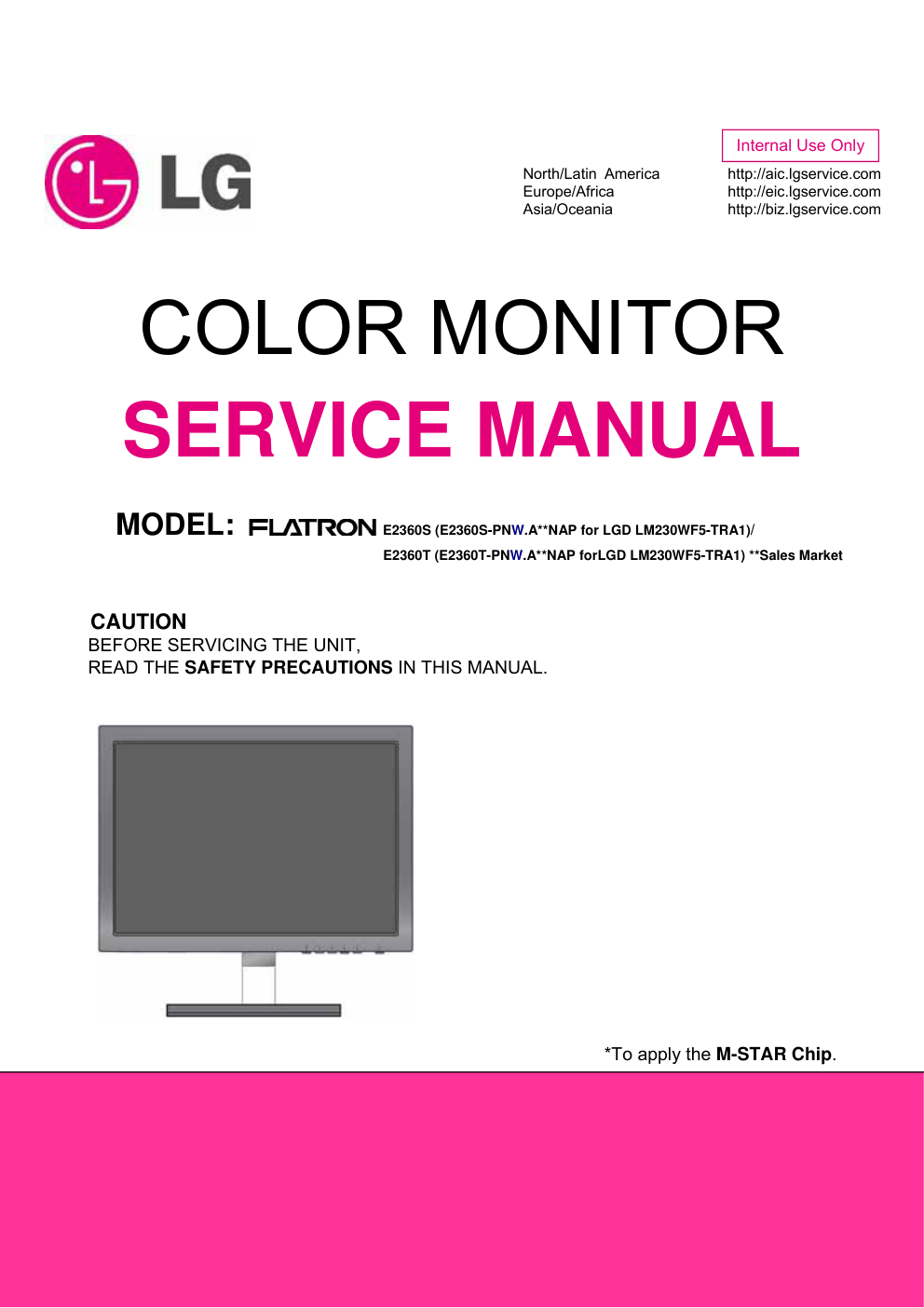
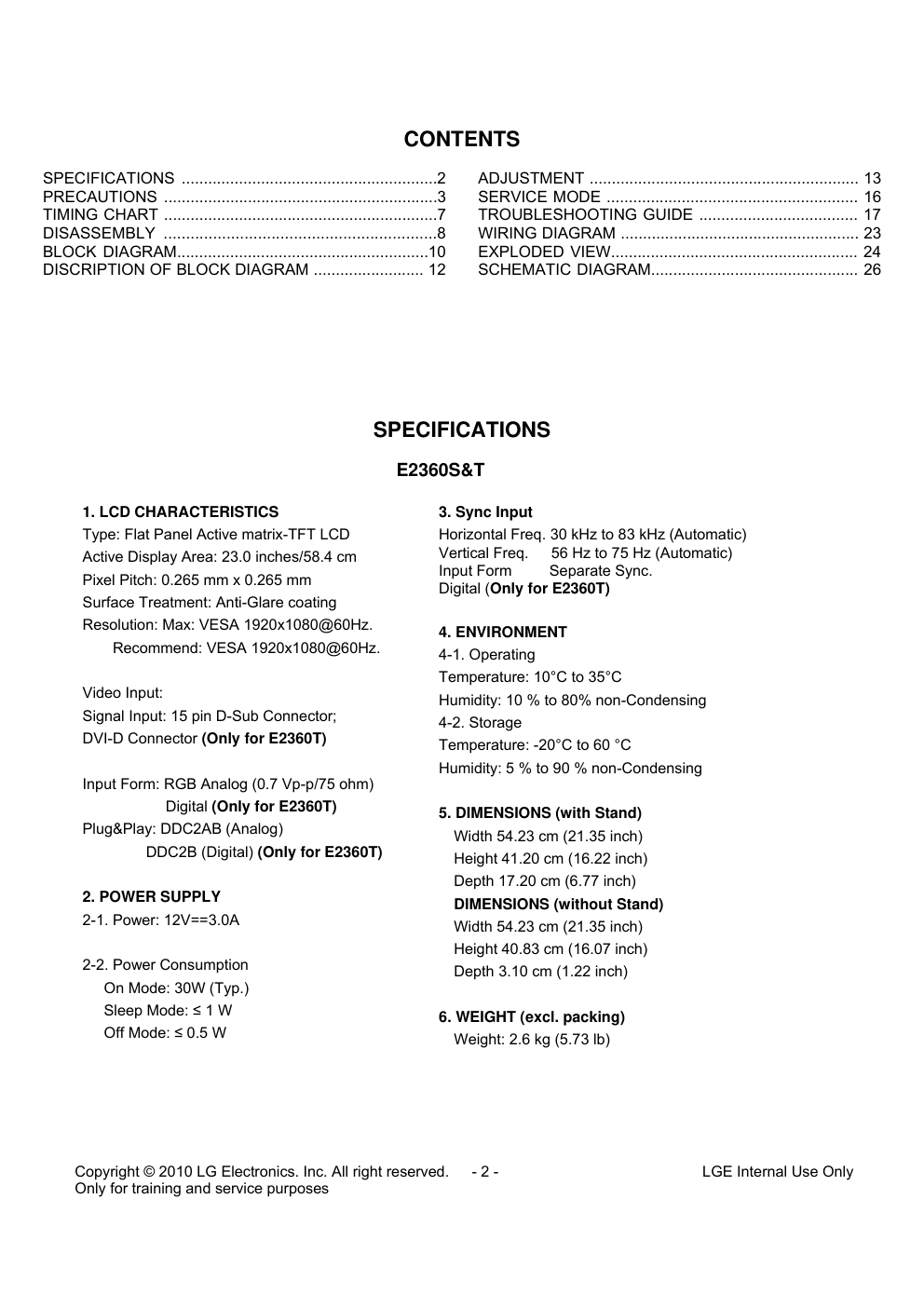
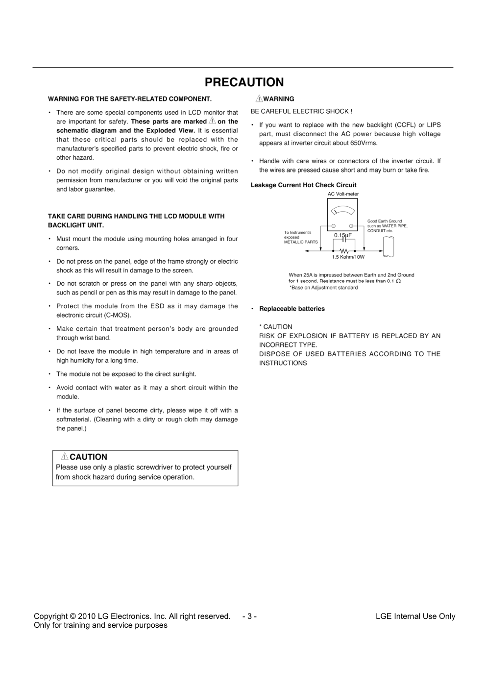
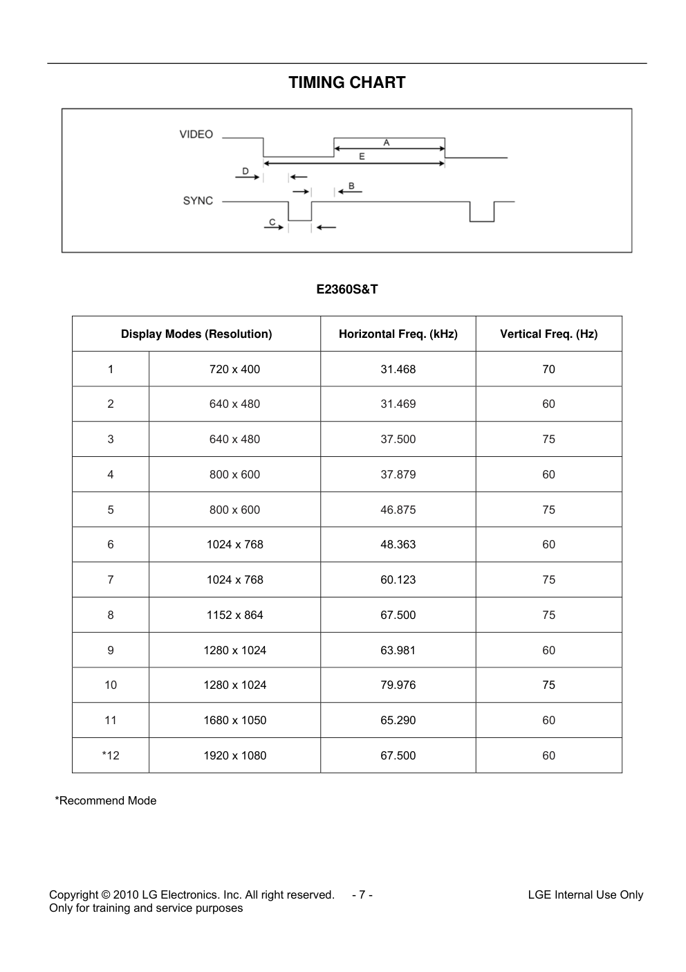
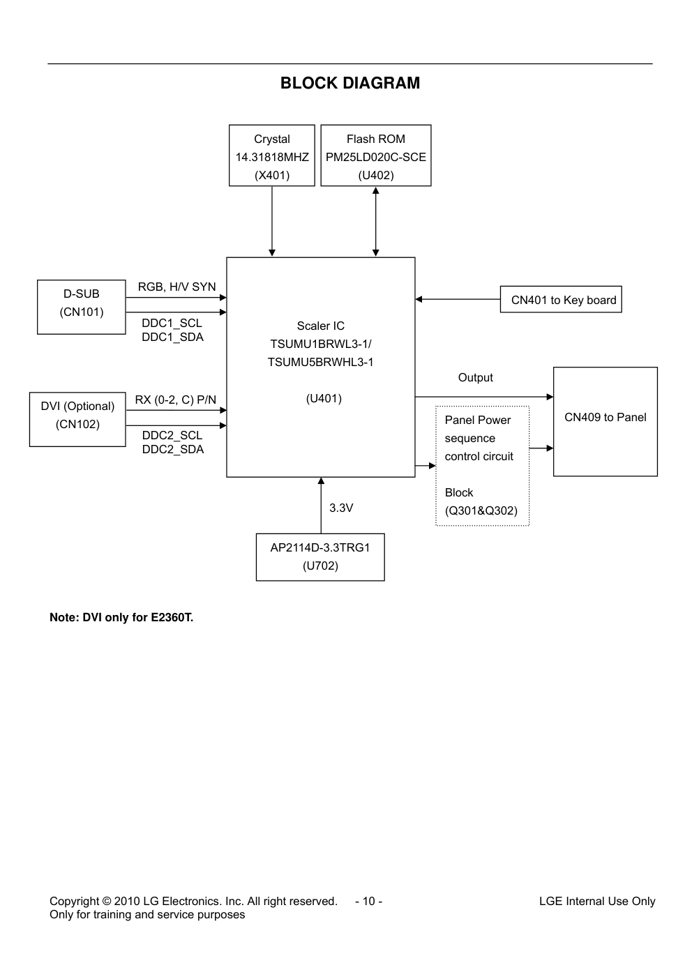
Copyright © 2010 LG Electronics. Inc. All right reserved. - 1 - LGE Internal Use Only Only for training and service purposes North/Latin America http://aic.lgservice.com Europe/Africa http://eic.lgservice.com Asia/Oceania http://biz.lgservice.com COLOR MONITOR SERVICE MANUAL MODEL: E2360S (E2360S-PNW.A**NAP for LGD LM230WF5-TRA1)/ E2360T (E2360T-PNW.A**NAP forLGD LM230WF5-TRA1) **Sales Market CAUTION BEFORE SERVICING THE UNIT, READ THE SAFETY PRECAUTIONS IN THIS MANUAL. *To apply the M-STAR Chip. Internal Use Only Copyright © 2010 LG Electronics. Inc. All right reserved. - 2 - LGE Internal Use Only Only for training and service purposes CONTENTS SPECIFICATIONS ..........................................................2 PRECAUTIONS ..............................................................3 TIMING CHART ..............................................................7 DISASSEMBLY .............................................................8 BLOCK DIAGRAM.........................................................10 DISCRIPTION OF BLOCK DIAGRAM ......................... 12 ADJUSTMENT ............................................................. 13 SERVICE MODE ......................................................... 16 TROUBLESHOOTING GUIDE .................................... 17 WIRING DIAGRAM ...................................................... 23 EXPLODED VIEW........................................................ 24 SCHEMATIC DIAGRAM............................................... 26 SPECIFICATIONS E2360S&T 1. LCD CHARACTERISTICS Type: Flat Panel Active matrix-TFT LCD Active Display Area: 23.0 inches/58.4 cm Pixel Pitch: 0.265 mm x 0.265 mm Surface Treatment: Anti-Glare coating Resolution: Max: VESA 1920x1080@60Hz. Recommend: VESA 1920x1080@60Hz. Video Input: Signal Input: 15 pin D-Sub Connector; DVI-D Connector (Only for E2360T) Input Form: RGB Analog (0.7 Vp-p/75 ohm) Digital (Only for E2360T) Plug&Play: DDC2AB (Analog) DDC2B (Digital) (Only for E2360T) 2. POWER SUPPLY 2-1. Power: 12V==3.0A 2-2. Power Consumption On Mode: 30W (Typ.) Sleep Mode: ≤ 1 W Off Mode: ≤ 0.5 W 3. Sync Input Horizontal Freq. 30 kHz to 83 kHz (Automatic) Vertical Freq. 56 Hz to 75 Hz (Automatic) Input Form Separate Sync. Digital (Only for E2360T) 4. ENVIRONMENT 4-1. Operating Temperature: 10°C to 35°C Humidity: 10 % to 80% non-Condensing 4-2. Storage Temperature: -20°C to 60 °C Humidity: 5 % to 90 % non-Condensing 5. DIMENSIONS (with Stand) Width 54.23 cm (21.35 inch) Height 41.20 cm (16.22 inch) Depth 17.20 cm (6.77 inch) DIMENSIONS (without Stand) Width 54.23 cm (21.35 inch) Height 40.83 cm (16.07 inch) Depth 3.10 cm (1.22 inch) 6. WEIGHT (excl. packing) Weight: 2.6 kg (5.73 lb) Copyright © 2010 LG Electronics. Inc. All right reserved. - 3 - LGE Internal Use Only Only for training and service purposes Copyright © 2010 LG Electronics. Inc. All right reserved. - 4 - LGE Internal Use Only Only for training and service purposes Copyright © 2010 LG Electronics. Inc. All right reserved. - 5 - LGE Internal Use Only Only for training and service purposes Copyright © 2010 LG Electronics. Inc. All right reserved. - 6 - LGE Internal Use Only Only for training and service purposes Copyright © 2010 LG Electronics. Inc. All right reserved. - 7 - LGE Internal Use Only Only for training and service purposes TIMING CHART E2360S&T Display Modes (Resolution) Horizontal Freq. (kHz) Vertical Freq. (Hz) 1 720 x 400 31.468 70 2 640 x 480 31.469 60 3 640 x 480 37.500 75 4 800 x 600 37.879 60 5 800 x 600 46.875 75 6 1024 x 768 48.363 60 7 1024 x 768 60.123 75 8 1152 x 864 67.500 75 9 1280 x 1024 63.981 60 10 1280 x 1024 79.976 75 11 1680 x 1050 65.290 60 *12 1920 x 1080 67.500 60 *Recommend Mode Copyright © 2010 LG Electronics. Inc. All right reserved. - 8 - LGE Internal Use Only Only for training and service purposes DISASSEMBLY-Set #1 Put the monitor on a soft flat. #2 Remove the base ass’y. Turn the screw by using the screw handle. #3 Remove the Rear Cover ass’y. #4 The Rear Cover ass’y. #5 Disconnect all the wires/FFC cable. #6 Remove the main frame. Copyright © 2010 LG Electronics. Inc. All right reserved. - 9 - LGE Internal Use Only Only for training and service purposes #7 Main frame and main board. #8 The panel. Note: DVI only for E2360T. Copyright © 2010 LG Electronics. Inc. All right reserved. - 10 - LGE Internal Use Only Only for training and service purposes BLOCK DIAGRAM Note: DVI only for E2360T. Scaler IC TSUMU1BRWL3-1/ TSUMU5BRWHL3-1 (U401) D-SUB (CN101) Crystal 14.31818MHZ (X401) CN401 to Key board RGB, H/V SYN DDC1_SCL DDC1_SDA Flash ROM PM25LD020C-SCE (U402) CN409 to Panel Output Panel Power sequence control circuit Block (Q301&Q302) AP2114D-3.3TRG1 (U702) 3.3V DVI (Optional) (CN102) RX (0-2, C) P/N DDC2_SCL DDC2_SDA Copyright © 2010 LG Electronics. Inc. All right reserved. - 11 - LGE Internal Use Only Only for training and service purposes CONVERTER BLOCK DIAGRAM Converter Boost Circuit Ignition LED bar ON/OFF circuit Current balance Control IC MP3389EF (U801) Feedback circuit OVP circuit Current Feedback DIM circuit 12V BKLT-EN BKLT-VBRI Copyright © 2010 LG Electronics. Inc. All right reserved. - 12 - LGE Internal Use Only Only for training and service purposes DESCRIPTION OF BLOCK DIAGRAM 1. Video Controller Part. This part amplifies the level of video signal for the digital conversion and converts from the analog video signal to the digital video signal using a pixel clock. The pixel clock for each mode is generated by the PLL. The range of the pixel clock is from 25MHz to 149MHz. This part consists of the Scalar, ADC converter, TMDS receiver. The Scalar gets the video signal converted analog to digital, interpolates input to 1920 x 1080 resolution signal and outputs 8-bit R, G, B signal to transmitter. 2. Power Part. This part consists of the one 3.3V regulators to convert power which is provided 12V in Adapter board, 12V is provided for convert circuit. 3. MICOM Part. This part is including video controller part. And this part consists of Reset IC and the Micom. The Micom distinguishes polarity and frequencies of the H/V sync are supplied from signal cable. The controlled data of each mode is stored in scalar. Copyright © 2010 LG Electronics. Inc. All right reserved. - 13 - LGE Internal Use Only Only for training and service purposes ADJUSTMENT Windows EDID V1.0 User Manual Operating System: DOS, windows98, 2000, XP 1. Parallel port setting Enter your bios, and do as followings. a) Integrated peripheral b) Super IO Device c) Parallel port mode you should set the” parallel port mode” to SPP for using the DOS EDID tool surely. 2. EDID Write 1. Connect the signal line of monitor with DDC recorder. 2. Choose the DDC RECORD program, and it shows on the screen, then choose the correct source base on the monitor. 3. Click “LoadFile”, then key in the manufacturer name, model name, product code, then choose the correct model name base on the monitor.(as Fig.2) 4. Scan serial No. to DDC recorder by Bar Reader, then read again in the Verify SN. 5. According to the message of DDC program, when the picture as fig.1 appears, it will show DDC record has finished. E2360S (Analog only) Copyright © 2010 LG Electronics. Inc. All right reserved. - 14 - LGE Internal Use Only Only for training and service purposes E2360T (Analog&DVI) Fig.1 Please check Manufacturer Name, Vendor Assigned Code, Monitor Name, Serial Number:*****[????????*****] (it must be the same as Bar Code),Week of Manufacture:**,Year of Manufacture:****,Checksum:** (It must be the same as the last byte of data table, as follows picture shows). Above of all must be right, then if it shows the green “PASS”, it means record succeeds ,the red “Fail” means record fails; Then check the power supply and signal line, and ensure they are connected well ,then do DDC record again from the third step. E2360S (Analog only) Copyright © 2010 LG Electronics. Inc. All right reserved. - 15 - LGE Internal Use Only Only for training and service purposes E2360T (Analog&DVI) Fig.2 Copyright © 2010 LG Electronics. Inc. All right reserved. - 16 - LGE Internal Use Only Only for training and service purposes 1) Turn off the power switch at the front side of the display. 2) Press MODE, POWER switch with 1 second interval, press MENU. 3) The SVC OSD menu contains additional menus that the User OSD menu as described below. a) CLEAA ETI: NO b) Auto Color: NO c) AGING: Select Aging mode (on/off). d) PANEL: Used panel type e) NVRAM INIT: NO f) R/G/B-9300K: Allows you to set the R/G/B-9300K value manually. g) R/G/B-6500K: Allows you to set the R/G/B-6500K value manually. h) R/G/B-Offset: Allows you to set the R/G/B-Offset value manually. (Analog Only) i) R/G/B-Gain: Allows you to set the R/G/B-Gain value manually. (Analog Only) e) R/G/B-sRGB: Allows you to set the R/G/B- sRGB value manually. SERVICE MODE Copyright © 2010 LG Electronics. Inc. All right reserved. - 17 - LGE Internal Use Only Only for training and service purposes TROUBLESHOOTING GUIDE 1. NO POWER No Power (Power Indicator Off) Please reinsert and make sure the AC of 100-240V is normal Measure U702 PIN2=3.3V Check the Adapter/convert section Check CN702 or replace U702 NO NO YES YES YES Check X401 oscillate waveforms are normal Replace X401 Replace U401 NO Copyright © 2010 LG Electronics. Inc. All right reserved. - 18 - LGE Internal Use Only Only for training and service purposes 2. NO RASTER (OSD IS NOT DISPLAY)-LIPS LIPS YES YES No Raster (OSD Is Not Displayed) Check U702 PIN 2 =3.3V? Check CN702 PIN3 =12V? Check adapter board and find out a short point as penning each power line 1. Check U702 2. Check C707,C708,C709 NO NO Copyright © 2010 LG Electronics. Inc. All right reserved. - 19 - LGE Internal Use Only Only for training and service purposes 3. NO RASTER (OSD IS NOT DISPLAY)-MSTAR 1. Check C426,C428 2. Check X401 3. Trouble in Scaler IC Scaler pin 98, 99 oscillates as 14.31818MHz? No Raster (OSD Is Not Displayed) Check connection line from D-SUB to Scaler Trouble in cable or LCD module NO YES YES NO Scaler IC pin 27 H Sync? pin 28 V Sync? Copyright © 2010 LG Electronics. Inc. All right reserved. - 20 - LGE Internal Use Only Only for training and service purposes 4. TROUBLE IN DPM Trouble in DPM Scaler IC pin 27 H Sync? pin 28 V Sync? Check H/V sync line Trouble in cable or LCD module NO YES Copyright © 2010 LG Electronics. Inc. All right reserved. - 21 - LGE Internal Use Only Only for training and service purposes 5. POWER Replace the panel Check main board Replace the main board NO Check CN702=12V? Check the adapter YES NO YES No Power (Power Indicator Off) Check AC line volt Check the adapter Check AC line & AC socket Replace the adapter NO YES NO Copyright © 2010 LG Electronics. Inc. All right reserved. - 22 - LGE Internal Use Only Only for training and service purposes 6. RASTER Check U401, X401 YES Check BKLT-VBRI Check U401 Check Q301, Q302 NO YES YES Check PANEL_VCC YES NO NO Raster (Lamp Off) Check CN702=12V Check BKLT-EN signal Check the adapter Check Interface section or main board NO NO Copyright © 2010 LG Electronics. Inc. All right reserved. - 23 - LGE Internal Use Only Only for training and service purposes WIRING DIAGRAM Main Board LED Board Key Board Optional Note: DVI only for E2360T. 095G176J-10V01 095G176J-50528 095G8022-7W506 Copyright © 2010 LG Electronics. Inc. All right reserved. - 24 - LGE Internal Use Only Only for training and service purposes EXPLODED VIEW Many electrical and mechanical parts in this chassis have special safety-related characteristics. These parts are identified by in the EXPLODED VIEW. It is essential that these special safety parts should be replaced with the same components as recommended in this manual to prevent X-RADIATION, Shock, Fire, or other Hazards. Do not modify the original design without permission of manufacturer. IMPORTANT SAFETY NOTICE Copyright © 2010 LG Electronics. Inc. All right reserved. - 25 - LGE Internal Use Only Only for training and service purposes EXPLODED VIEW PARTS LIST Ref. No. TPV part No. LGE part No. Description 010 705GFACS016 ABJ73308504 BEZEL ASS'Y 020 KEPCAQG1 EBU60704503 KEY BOARD 030 LEPCAQG1 EBU60934810 LED BOARD 040 750GMT230W5A11M0LG COV30101224 PANEL LM230WF5-TRA1-7F1-A0 FQ LTD 050 756GQACB-KL010--00 EBU60714340 MAIN BOARD(CBPCAAWLGQ3)-E2360S 756GQACB-KL009--00 EBU60714341 MAIN BOARD(CBPCAARLGQ3)-E2360T 060 Q15G0909101101 MDQ62638101 MAINFRAME-E2360S Q15G0909101201 MDQ62638102 MAINFRAME-E2360T 070 705GFACS012 ACQ83873708 REAR COVER ASS'Y-E2360S 705GFACS013 ACQ83873709 REAR COVER ASS'Y-E2360T 080 705GFACS004 ACQ83873802 BASE ASS'Y 090 095G176J-10V01 COV30101415 FFC CABLE 10PIN 275MM 0.5MM 100 095G176J-50528 COV30101418 FFC CABLE 50 182 0.5 110 095G8022-7W506 N/A HARNESS 7P-6P+3P 250/300 120 088G-35315FVCL N/A D-SUB CABLE 1500MM Copyright © 2010 LG Electronics. Inc. All right reserved. - 26 - LGE Internal Use Only Only for training and service purposes SCHEMATIC DIAGRAM E2360S&T Input (DVI only for E2360T) DET_VGA DDC_VCC DSUB_SCL DDC1_SCL DDC_VCC R102 0R01 1/10W C106 47N16V C105 5PF 50V ZD101 RLZ5.6B C108 47N16V R132 NC/10OHM1/16W FB106 NC/300 OHM R110 470 OHM 1/16W R111 56OHM1/16W C110 47N16V C118 NC/1N 50V R130 NC/10OHM1/16W C119 NC/1N 50V R127 NC/10OHM1/16W R103 1K 1/16W FB103 0R01 1/10W C125 100N 16V R107 2.2K 1/16W C128 NC C109 5PF 50V I/O1 1 GND 2 I/O2 3 I/O3 4 VDD 5 I/O4 6 U107 NC/AZC199-04S C114 47N16V C127 NC R114 56OHM1/16W C122 NC/100N 16V DAT2- 1 DAT2+ 2 2/4shield 3 DAT4- 4 DAT4+ 5 DDC SCL 6 DDC SDA 7 VSYNC 8 DAT1- 9 DAT1+ 10 1/3shield 11 DAT3- 12 DAT3+ 13 +5V 14 SYNC GND 15 HPD 16 DAT0- 17 DAT0+ 18 0/5shield 19 DAT5- 20 DAT5+ 21 clk shield 22 clk+ 23 clk- 24 GND 26 GND 25 CN102 JACK I/O1 1 GND 2 I/O2 3 I/O3 4 VDD 5 I/O4 6 U104 AZC199-04S R116 75OHM 1/16W R134 NC/10OHM1/16W R125 4.7K 1/16W C103 22P 50V C126 100N 16V C117 NC/220N16V R112 75OHM 1/16W C112 NC/100N 16V C111 47N16V FB102 0R01 1/10W R138 NC/4.7K 1/16W I/O1 1 GND 2 I/O2 3 I/O3 4 VDD 5 I/O4 6 U106 NC/AZC199-04S R124 4.7K 1/16W R137 NC/4.7K 1/16W R115 56OHM1/16W R113 100OHM1/16W R139 NC/1K 1/16W I/O1 1 GND 2 I/O2 3 I/O3 4 VDD 5 I/O4 6 U105 NC/AZC199-04S R120 NC/10K+-5%1/16W FB101 0R01 1/10W 3 1 2 D101 BAV70 R108 75OHM 1/16W R135 2.2K 1/16W C115 NC/100N 16V A0 1 A1 2 A2 3 VSS 4 SDA 5 SCL 6 WP 7 VCC 8 U102 NC/CAT24C02WI-GT3 R136 NC/22K 1/16W R126 NC/10OHM1/16W R119 NC/100OHM1/16W C124 100N 16V R117 56OHM1/16W C116 220N16V R128 NC/10OHM1/16W C104 22P 50V C102 47N16V FB105 NC/300 OHM C120 NC/100N 16V R101 100OHM1/16W R131 NC/10OHM1/16W R105 56OHM1/16W R123 22K 1/16W C121 NC/100N 16V A0 1 A1 2 A2 3 VSS 4 SDA 5 SCL 6 WP 7 VCC 8 U101 NC/CAT24C02WI-GT3 R104 1K 1/16W FB104 NC/300 OHM R109 56OHM1/16W C107 1N 50V 3 1 2 D102 NC/BAV70 C113 5PF 50V R129 NC/10OHM1/16W R118 NC/100OHM1/16W 1 6 2 7 3 8 4 9 5 11 12 13 14 15 10 17 16 CN101 D-SUB 15P R106 2.2K 1/16W R133 3.9K1/16W I/O1 1 GND 2 I/O2 3 I/O3 4 VDD 5 I/O4 6 U103 AZC199-04S CMVCC1 3,4,5 ESD_VCC DVI_5V ESD_VCC1 VCC3.3 ESD_VCC CMVCC1 ESD_VCC1 DVI_5V DSUB_5V ESD_VCC1 DVI D-SUB DDC_WP 5 DDC2_SDA 5 RX1N 5 DSUB_V 5 DDC1_SCL 5 RX1P 5 RX0N 5 DET_CABLE 5 DDC1_SDA 5 RXCP 5 RX0P 5 DSUB_H 5 DDC2_SCL 5 DDC_WP 5 RX2N 5 RXCN 5 DSUB_G- 5 DSUB_G+ 5 RX2P 5 DSUB_SOG 5 DSUB_B+ 5 DSUB_B- 5 DSUB_R+ 5 DSUB_R- 5 VGA_R- DSUB_SCL DSUB_SDA VGA_R+ VGA_B+ VGA_G+ V_Sy nc VGA_G- DDC1_SDA DSUB_SDA H_Sy nc DDC1_SCL DDC2_SDA DDC2_SCL DVI_HPD H_Sy nc DDC1_SDA VGA_B- DDC2_SDA V_Sync DSUB_5V RX1P DET_DVI VGA_R+ DDC2_SCL VGA_B+ RX2P ESD_VCC DET_VGA VGA_G- VGA_G+ RX0N VGA_R- VGA_B- VGA_G+ VGA_B+ RXCN ESD_VCC1 RX1N RX0P VGA_R+ DET_DVI RX2N RXCP DET_VGA 1. Main Board Copyright © 2010 LG Electronics. Inc. All right reserved. - 27 - LGE Internal Use Only Only for training and service purposes Output LV0- LV0+ LV5- LV5+ LV4- LV4+ LV3- LV3+ FLK24 P26 ICLK4 P23 IVDD_O P24 IVDD_E P25 ICLK3 P22 FLK13 P27 ICLK2 P21 ICLK1 P20 POL P16 POL2 P15 CSC P17 LV1- P10 LV1+ P11 LV0- P12 LV0+ P13 SOE P14 H2DOT P18 ICLK_RESET P19 AO3401L 2 1 PSDA S D S 1 S 2 S 3 G 4 D 8 D 7 D 6 D 5 U301 NC/AO4411 3 C305 1UF16V Q301 AO3401A PSCL G 1 2 3 4 5 6 7 8 9 10 11 12 13 14 15 16 17 18 19 20 21 22 23 24 25 26 27 28 29 30 31 32 33 34 35 36 37 38 39 40 41 42 43 44 45 46 47 48 49 50 51 52 CN409 CONN R303 4.7K 1/16W Q302 LMBT3904LT1G R307 NC 1 2 FB301 120 OHM C301 100N 16V R306 100K 1/16W C302 22UF 16V C303 220N16V R304 22K 1/16W R305 10K+-5%1/16W C304 100N 16V CMVCC1 2,4,5 PANEL_VCC CMVCC1 PANEL_VCC CMVCC1 P[0..27] 5 PSCL 5 PSDA 5 PPWR_ON# 5 P6 LCLK- P5 LV3+ P0 LV5- P4 LV3- P3 LV4+ P1 LV5+ P7 LCLK+ P[0..27] FLK13 FLK24 P8 LV2- IVDD_E IVDD_O ICLK4 ICLK3 ICLK2 ICLK1 ICLK_RESET H2DOT POL POL2 SOE R302 300 OHM R301 300 OHM CSC P9 LV2+ P2 LV4- LCLK- LCLK+ LV2- LV2+ LV1- LV1+ Copyright © 2010 LG Electronics. Inc. All right reserved. - 28 - LGE Internal Use Only Only for training and service purposes Power 2010/3/23 Place a large Pad with TOP SOT 252 SOT 223 SOT 263 SOT 252 3 2 1 CN702 JACK VIN 3 VOUT 2 GND 1 U701 NC/G1084-33TU3Uf VIN 3 VOUT 2 GND 1 U703 NC/LSP2159BD18AD R702 10K+-5%1/16W C720 10uF 25V C709 100N 16V C724 NC/1UF16V C723 10uF 25V R705 10K+-5%1/16W C713 100NF 25V 1 2 D703 SR34 C706 100N 16V R703 10K+-5%1/16W VI 3 VO 2 GND 1 U704 AP2114H-1.8TRG1 R713 7.5K 1% R712 100K 1/16W C704 22UF 16V 1 2 D704 SR34 R706 100OHM1/16W C715 1N 50V R726 100K 1/16W Q701 LMBT3904LT1G C712 100NF 25V + C716 470uF 10V C708 100N 16V 1 2 D701 SM340A 1 2 D707 SR34 SW 1 EN 2 COMP 3 FB 4 GND 5 FREQ 6 VIN 7 BST 8 Thermal Pad 9 U705 MP1584EN C721 100N 16V C702 100N 16V C717 100N 16V 1 2 FB701 BEAD C722 150pF 50V R714 1.3K 1% R727 300K 1 2 D708 SR34 C719 100NF 25V C707 22UF 16V R711 33K 1/16W 5% C705 100N 16V 1 2 FB702 30R/700mA R704 22K 1/16W + C718 180uF 16V 3 2 1 CN701 NC/JACK VIN 3 VOUT 2 GND 1 U702 AP2114D-3.3TRG1 L701 22UH C710 1N 50V 1 2 ZD702 NC/RLZ6.2B CMVCC1 CMVCC1 CMVCC1 2,3,5 VCC1.8 CMVCC1 CMVCC1 CMVCC1 VCC3.3 VCC3.3 on_BACKLIGHT 5 +12V BKLT-VBRI 6 BKLT-EN 6 adj_BACKLIGHT 5 +12V 6 LGE Used OTS Used Copyright © 2010 LG Electronics. Inc. All right reserved. - 29 - LGE Internal Use Only Only for training and service purposes Scaler R406 10K+-5%1/16W R433 3.9K1/16W R440 10K+-5%1/16W R415 0R05OHM1/16W R444 0R05OHM1/16W C427 10uF 10V R418 NC/0R05OHM1/16W C417 100N 16V C402 100N 16V C426 47pF 50V 2 4 6 1 3 5 CN402 NC/CONN ZD402 NC/RLZ5.6B R436 100OHM1/16W R442 NC C401 100N 16V R437 100OHM1/16W C440 NC C415 100N 16V NC 1 E1 2 E2 3 VSS 4 SDA 5 SCL 6 WC 7 VCC 8 U403 NC/M24C04-WMN6TP 1 2 X401 14.31818MHZ/32PF R451 100 OHM 1/10W WP Q403 NC/LMBT3904LT1G C407 100N 16V C416 100N 16V C436 100N 16V ZD403 NC/RLZ5.6B C435 100N 16V C418 100N 16V C434 100N 16V 1 2 FB409 120 OHM VCC3.3 2,4 VCC3.3 VCC1.8 4 VDDC VDDP VCC3.3 CMVCC1 VCC1.8 VCC3.3 AVDD VDDC CMVCC1 AVDD VCC3.3 VDDP VCC3.3 VCC3.3 DDC1_SCL 2 DSUB_H 2 DSUB_R+ 2 DSUB_G+ 2 RX1N 2 RX0N 2 adj_BACKLIGHT 4 DSUB_V 2 DET_CABLE 2 DDC2_SCL 2 DDC1_SDA 2 DSUB_SOG 2 RXCP 2 DSUB_R- 2 DDC2_SDA 2 DSUB_G- 2 RX1P 2 RX2P 2 RX0P 2 DSUB_B- 2 DDC_WP 2 DSUB_B+ 2 RXCN 2 RX2N 2 P[0..27] 3 PSDA 3 PSCL 3 PSCL 3 on_BACKLIGHT 4 PPWR_ON# 3 PPWR_ON# 3 PSDA 3 TSUMU1BRWL3 56G 562344 1Analog+1DVI TSUMU5BRWHL3-1 56G 562342 TSUMU1BRWL3-1 56G 562345 TSUM5ARWHL3 56G 562346 UXGA / WSXGA+ (1680x1050,1600x900) 1Analog WXGA / WXGA+ (1440x900/1366x768/1280x1024) TSUMU5BRWHL3 56G 562347 U401 TSUM1ARWL3 56G 562343 WUXGA / FHD (1920x1200/1920x1080) C406 100N 16V TOUCH P[0..27] C422 2.2UF 16V Panel_ON AHS0 AVS0 B0- B0+ SOG_DET G0+ G0- R0+ R0- LED_ORANGE LED_GRN/BLUE DDCSDA1 RIN0P 26 GIN0P 23 SOGIN0 24 BIN0P 21 RIN0M 25 GIN0M 22 BIN0M 20 HSYNC0 27 VSYNC0 28 SDO 36 SCK 38 CSZ 37 SDI 39 FLK24 49 GPIO_P43/PWM0 1 LV4+ 75 XOUT 98 XIN 99 LV3- 74 LV3+ 73 LVCLK- 72 LVCLK+ 71 LV2- 70 LV2+ 69 LV1- 68 LV1+ 67 LV0- 66 LV0+ 65 SOE 62 POL2 61 POL 60 CSC 59 H2DOT 58 ICLK_RESET/GSP 56 LV4- 76 LV5+ 78 LV5- 79 GND 2 GND 8 NC 6 NC 7 NC 9 NC 10 AVDD_33 11 NC 12 NC 13 NC 15 NC 16 GND 14 GND 17 GND 45 VDDP 77 VDDP 57 MODE 29 VCTRL 80 VDDC 19 DDCA_SDA/RS232_TX 30 DDCA_SCL/rs232_RX 31 NC 3 NC 4 GPIO_P40/PWM1 32 AVDD_33 18 VDDP 83 IVDD_E/GOE 50 GPIO_P06/PWM1 93 FLK13 48 GPIO_P00/SAR1 90 GPIO_P01/SAR2 91 GPIO_P02/SAR3 92 GPIO_P07/PWM2 94 GPIO_P23/PWM1 5 GPIO_P41/PWMA 41 GPIO_P13/PWM3 96 GPIO_P26/PWM0 95 I2C_MDA/GPIO_P11 33 I2C_MCL/GPIO_P10 34 RST 84 ICLK4 52 IVDD_O/DPM 51 AVDD_33 100 VDDP 35 VDDP 47 VDDC 40 VDDC 63 VDDC 81 GND 64 GND 82 GPIO_P17/SAR0 89 ICLK1/GSC 55 ICLK2 54 ICLK3 53 GPIO_P42/PWMB 42 GPIO_P24/PWM2 43 GPIO_P27/PWM2 44 GPIO_P12 46 GPIO_P12/PWM3 85 GPIO_P25/PWM1 86 GPIO_P08 87 GPIO_P09 88 VDDC 97 TSUMU1BRWL3-LF-1 U401 RX0- DDCSDA2 GPIO wakeup input: GPIO_P43 (GPIO source 0) #1 GPIO_P40 (GPIO source 1) #32 GPIO_P25 (GPIO source 2) #86 GPIO_P41 (GPIO source 3) #41 DVI 5V detection (0) PAD_GPIO_08:pin #87 (BK4_23h[1:0] set 0) (1) PAD_GPIO_12:pin #46 (BK4_23h[1:0] set 2) RX2+ LED_R RX0+ KEY2 KEY1 KEY2 MSCL MSDA RXC+ RX1- LED_G RX1+ RXC- KEY1 POWER_KEY# DET_CABLE POWER_KEY# DDCSCL1 DDCSCL2 RX2- EE_WP CMVCC1 CMVCC1 2,3,4 R405 0R01 1/10W R412 10K 1/16W 5% R404 0R01 1/10W R410 2K2 1/16W 5% LED_R LED_G 1 2 3 Q401 LMBT3906LT1G 1 2 3 Q402 LMBT3906LT1G P20 R411 2K2 1/16W 5% LED_GRN/BLUE R413 10K 1/16W 5% CMVCC1 LED_ORANGE adj_BACKLIGHT KEY1 POWER_KEY# LED_R KEY2 LED_G KEY2 LED_G KEY1 POWER_KEY# LED_R TOUCH MSDA EE_WP P25 P7 P19 P10 P23 P14 P17 P12 P18 P24 P26 P11 P16 P13 P21 P2 P22 P8 P5 P4 P3 P1 P15 P27 P6 P0 P9 WP DDC_WP on_BACKLIGHT R450 NC/10K+-5%1/16W R414 100OHM1/16W C432 100N 16V R431 3.9K1/16W R435 NC/22K1/16W 1 3 5 7 2 4 6 CN403 NC/CONN C413 10uF 10V CE# 1 SO 2 WP# 3 GND 4 VDD 8 HOLD# 7 SCK 6 SI 5 U402 Pm25LD020C-SCE R402 10K+-5%1/16W R432 3.9K1/16W C414 100N 16V 1 2 3 4 5 6 7 CN401 CONN R420 NC/0R05OHM1/16W ZD401 NC/RLZ5.6B FB401 300OHM C403 100N 16V R401 100OHM1/16W 1 2 FB408 NC/120 OHM C428 47pF 50V R441 10K+-5%1/16W FB403 300OHM MSCL R728 0R05OHM1/16W C433 100N 16V R416 0R05OHM1/16W R419 NC/0R05OHM1/16W R426 100OHM1/16W R403 100K1/16W C421 100N 16V R443 0R05OHM1/16W C441 NC FB402 300OHM C429 220N16V C423 100N 16V C431 100N 16V Copyright © 2010 LG Electronics. Inc. All right reserved. - 30 - LGE Internal Use Only Only for training and service purposes Convert R809 6.2KOHM +-1% 1/10W +C807 4.7UF 100V Set WLED current for current limit Set OVP R842 2.2 OHM 1/10W R816 0.3 OHM R812 0.3 OHM R834 200KOHM 1/10W R805 300K 1/8W R827 1R 1/10W 5% C804 0.47UF 50V C802 68NF 50V R806 1K 1/10W C801 0.47uF 16V R819 30KOHM +-1% 1/10W R810 20K 1/10W L801 47UH 1 2 D801 SK310B + C811 180uF 16V R830 1R 1/10W 5% 1 2 3 4 5 6 7 8 9 10 11 12 CN803 CONN C809 100pF 50V R818 0R05 1/4W NC 1 VIN 2 VCC 3 COMP 4 EN 5 DBRT 6 GND 7 OSC 8 ISET 9 BOSC 10 LED12 11 LED11 12 LED10 13 LED9 14 LED8 15 LED7 16 LED6 17 LED5 18 LED4 19 LED3 20 LED2 21 LED1 22 OVP 23 ISENSE 24 PGND 25 GATE 26 VFAULT 27 NC 28 E-Pad 29 U801 MP3389EF C806 100pF 50V R836 0R01 1/10W R808 1K 1/10W R841 150 OHM 1/10W R801 10 OHM 1/10W R807 20K 1/10W R832 0R01 1/10W R829 NC/1 OHM 1/10W R840 0R01 1/10W C805 100pF 50V R803 51KOHM +-1% 1/10W R802 270K +-1% 1/10W R831 NC/1 OHM 1/10W C810 1uF 25V R804 100K 1/10W R828 1R 1/10W 5% R813 0R05 4A 1/4W R833 NC/0R01 1/10W R839 NC/0R01 1/10W S1 1 G1 2 S2 3 G2 4 D1 8 D1 7 D2 6 D2 5 Q806 P8008HV C803 0.47UF 50V GND_POWER +12V GND_POWER DGND GND_POWER GND_POWER GND_POWER GND_POWER +12V 4,6 GND_POWER GND_POWER GND_POWER BKLT-VBRI 4 BKLT-EN 4 OVP R832,R836,R840-->0ohm R831,R829,R833,R839-->NC R828-->1ohm R819-->30K ---Set WLED current R809 5.6K ---Set OVP R812-->0.15ohm for current limit R833,R839-->0ohm R831,R832,R836,R840-->NC R828,R829-->1ohm R819-->10K ---Set WLED current R809 5.6K ---Set OVP R812-->0.15ohm ---for current limit LM185WH2-TRA1 LM215WF4-TRA1 WXGA+ (1366x768) / 18.5〃 Panel Size & Resolution LM200WD3-TRA1 FHD (1920x1080) / 23〃 Panel Type Different table LM230WF5-TRA1 FHD (1920x1080) / 21.5〃 WSXGA+ (1600x900) / 20〃 OVP Copyright © 2010 LG Electronics. Inc. All right reserved. - 31 - LGE Internal Use Only Only for training and service purposes 1 2 ZD006 MLVS0402M04 MENU GND 1 2 4 3 5 SW001 SW EXIT LBADC1 LBADC2 AUTO POWER 1 2 4 3 5 SW002 SW 1 2 4 3 5 SW003 SW R001 3K3 1/10W 1% 1 2 4 3 5 SW004 SW 1 2 ZD001 MLVS0402M04 1 2 4 3 5 SW005 SW 1 2 4 3 5 SW006 SW 1 2 3 4 5 6 7 8 CN001 CONN R002 2K2 1/10W 1% R005 2K2 1/10W 1% 1 Power EXIT SOURCE AUTO MODE MENU CON001 R003 1.5K +-1% 1/10W MODE R004 3K3 1/10W 1% R006 1.5K +-1% 1/10W SOURCE 6P GND C002 100N16V 1 2 ZD002 MLVS0402M04 C001 100N16V 1 2 ZD003 MLVS0402M04 1 2 ZD004 MLVS0402M04 1 2 ZD005 MLVS0402M04 2. Key Board Copyright © 2010 LG Electronics. Inc. All right reserved. - 32 - LGE Internal Use Only Only for training and service purposes 1 2 3 4 5 CN002 CONN C012 100N16V LED_BLUE CN002 LED B/R 1 2 3 4 RED BLUE LED002 LED 1 2 3 4 RED BLUE LED003 LED 1 LED_RED LED B/R LED B/R Right Angle GND 1 2 3 4 RED BLUE LED001 LED C011 100N16V 3. LED Board Copyright © 2010 LG Electronics. Inc. All right reserved. - 33 - LGE Internal Use Only Only for training and service purposes Jul.2010 P/NO: Printed in China
版权声明
1. 本站所有素材,仅限学习交流,仅展示部分内容,如需查看完整内容,请下载原文件。
2. 会员在本站下载的所有素材,只拥有使用权,著作权归原作者所有。
3. 所有素材,未经合法授权,请勿用于商业用途,会员不得以任何形式发布、传播、复制、转售该素材,否则一律封号处理。
4. 如果素材损害你的权益请联系客服QQ:77594475 处理。