LG CF-14K49E彩电维修手册和原理图
 "LG CF-14K49E彩电维修手册和原理图-0")
 "LG CF-14K49E彩电维修手册和原理图-1")
 "LG CF-14K49E彩电维修手册和原理图-2")
 "LG CF-14K49E彩电维修手册和原理图-3")
 "LG CF-14K49E彩电维修手册和原理图-4")
 "LG CF-14K49E彩电维修手册和原理图-5")
 "LG CF-14K49E彩电维修手册和原理图-6")
 "LG CF-14K49E彩电维修手册和原理图-7")
 "LG CF-14K49E彩电维修手册和原理图-8")
 "LG CF-14K49E彩电维修手册和原理图-9")
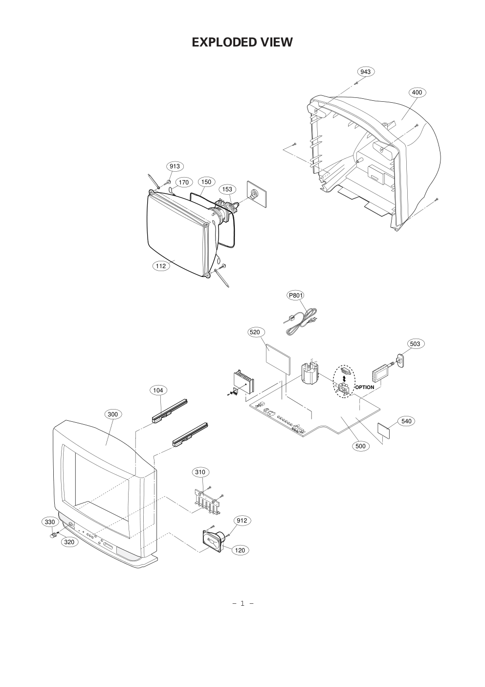
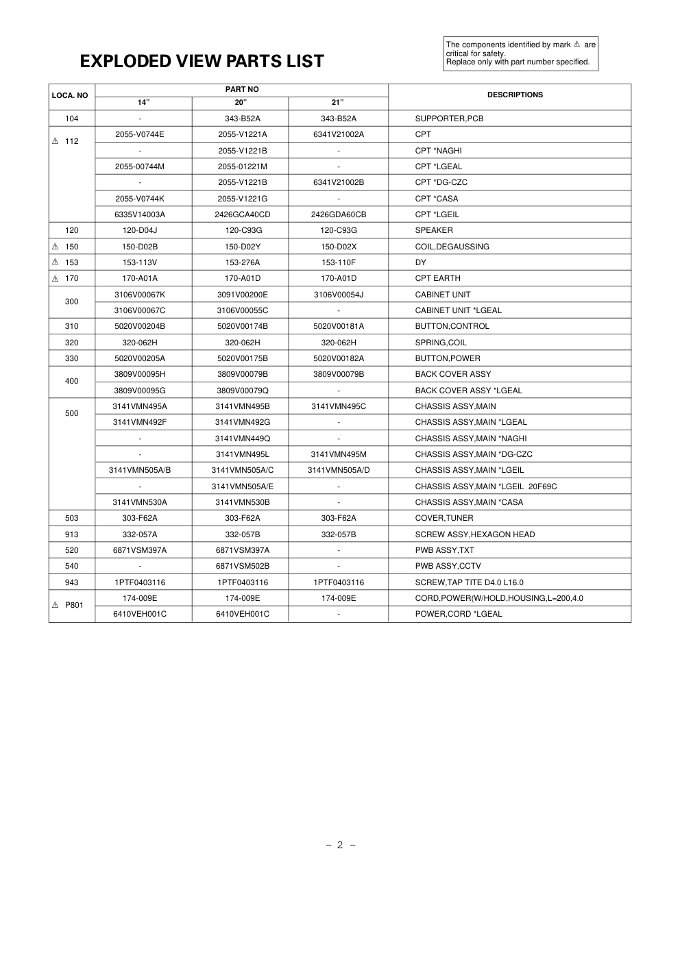
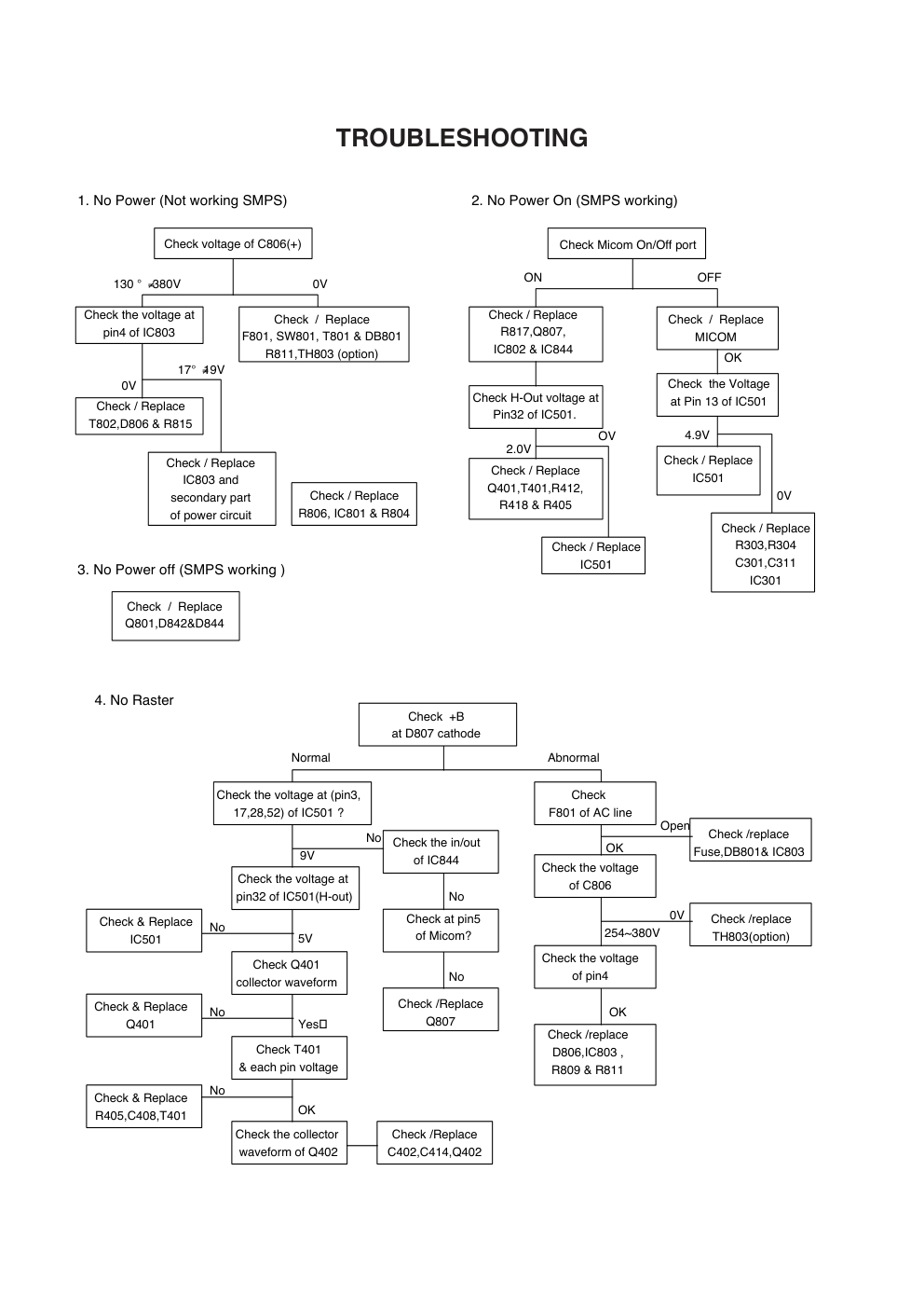
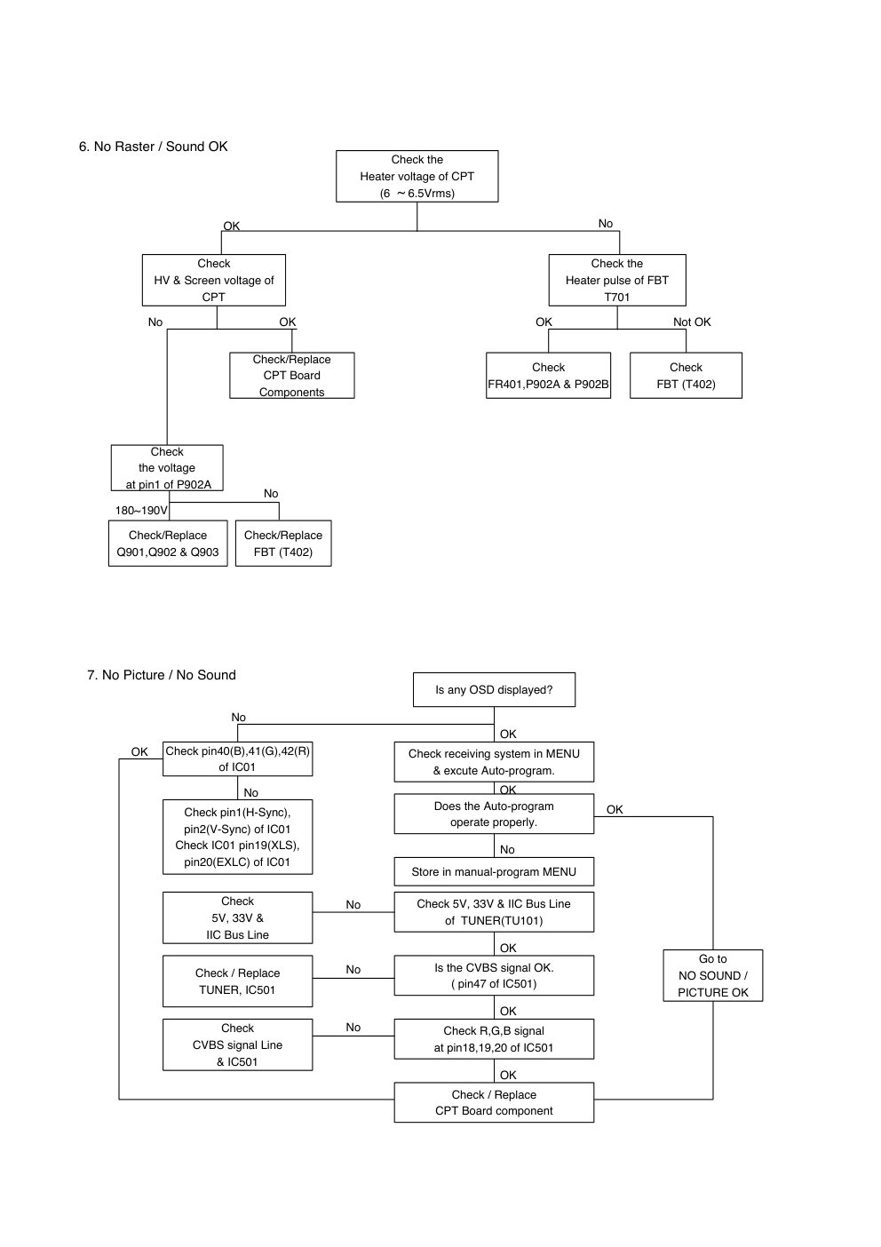
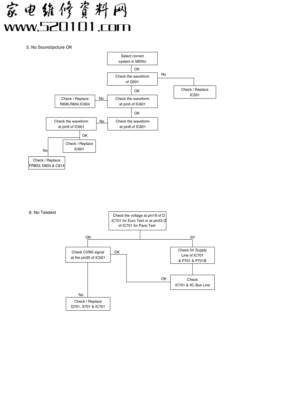
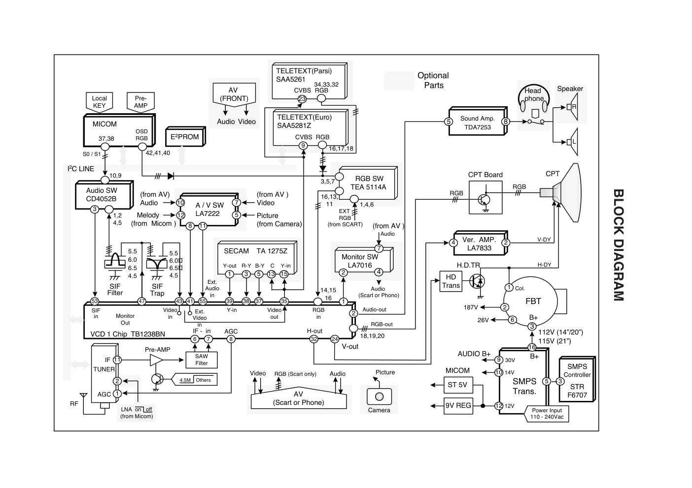
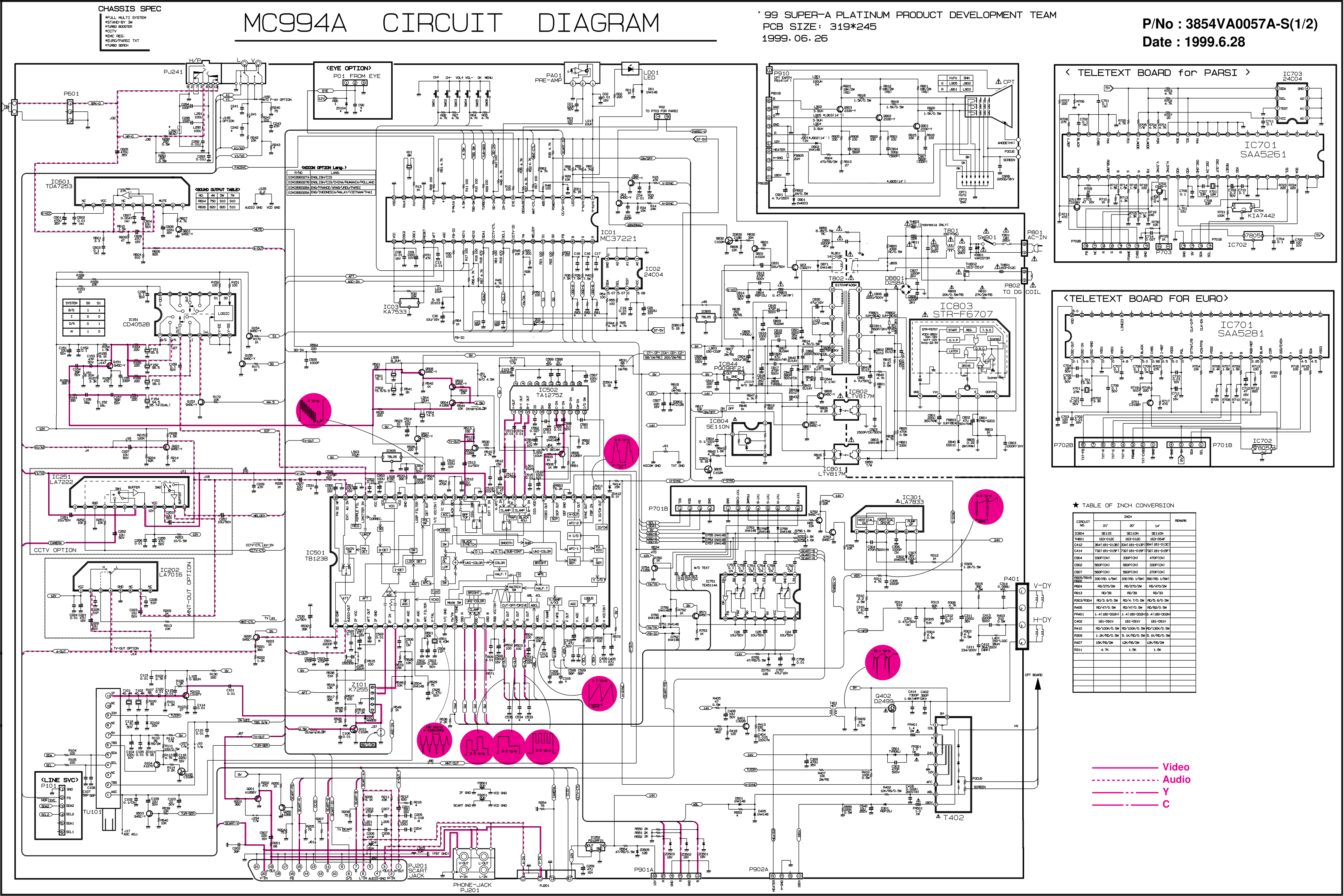
- 1 - Y Safety Precautions 1. It is safe to adjust after using insulating transformer between the power supply line and chassis input to prevent the risk of electric shock and protect the instrument. 2. Never disconnect leads while the TV receiver is on. 3. Don't short any portion of circuits while power is on. 4. The adjustment must be done by the correct appliances. But this is changeable in view of productivity. 5. Unless otherwise noted, set the line voltage to 230Vac!10%, 50Hz. Y Test Equipment required 1. RF signal generator (with pattern generator) 2. DC Power Supply 3. Multimeter (volt meter) 4. Oscilloscope 5. Color analyzer : RF AGC (Automatic Gain Control) Adjustment The RF AGC was aligned at the time of manufacture for optimum performance over a wide range conditions. Readjustment of RF AGC should not be necessary unless unusual local conditions exist, such as ; 1) Channel interference in a CATV system. 2) Picture bending and/or color beats, which are unusually due to excessive RF signal input when the receiver is too close to a transmitting tower or when the receiver is connected to an antenna distribution system where the RF signal has been amplified. In this case, the input signal should be attenuated (with pad or filter) to a satisfactory level. 3) Picture noise caused by "broadcast noise" or weak signal. If the broadcast is "clean" and the RF signal is at least 1mV (60dBu), the picture will be noise free in any area. Adjusting RF AGC to one end of rotation will usually cause a relatively poor signal to noise ratio; Adjusting to the other end of rotation will usually cause a degradation of over load capabilities resulting in color beats or adjacent channel interference. : Screen Voltage Adjustment 1) Input the Color Bar Pattern into Antenna jack. 2) Select CutOff of SVC-3 mode. 3) Turn the screen control clockwise until the Horizontal line is visible and turn it counterclockwise until the Horizontal line is faintly visible. : Focus Adjustment NOTE: This adjustment should be performed after warming up for 10 minutes. 1) Input the Color Bar Pattern into Antenna jack. 2) Adjust the Focus control of FBT for best overall focus. : VCO Adjustment 1) Input Digital Pattern into Antenna jack. 2) Select A-PIF of SVC-4 mode. 3) Press VOLF/G button and A-PIF will be changed 0 to 1 while the number of PIF-C is rolling. 4) When PIF-C stops rolling, A-PIF will be changed 1 to 0 and VCO adjustment is finished. Caution : Do not press the Volume button again in A-PIF mode after adjustment is finished. Adjustment 1. Connect RF signal (65dB!0.5dB) and turn on the TV. 2. Press OK buttons on TV set and Remote Controller at the same time to get into SVC mode. 3. Press Channel UP/DOWN button on the Remote Controller several times to find AGC. 4. Press Volume UP/DOWN button until the AGC Voltage is the same as the Table below. 5. Press OK(Y) button to memorize the data. 1. To get into SVC mode 1) Press OK buttons on both TV set and Remote Control at the same time. 2) Press Yellow button to select OPTION-1, OPTION-2, OPTION-3 or OPTION-4. 3) Press PR E/D button to select an adjustment. 4) Press VOL F/G button to change the data. 2. To memorize the adjusted data into EEPROM Press OK button. 3. To get out from SVC mode Press TV/AV or Power button. Test Point : AGC TP (J17) Adjust : Remote Control Test Point : RK (Red Cathode of CPT Board) Adjust : Screen Control of FBT TUNER AGC Voltage Default AGC Data 6700VPV002A(LG C&D) 2.5 ! 0.1V 24 6700VPV002B(LG C&D) 3.0 ! 0.1V 24 Test Point : Observing Display Adjust : Focus control of FBT ADJUSTMENT - 2 - : Deflection Data Adjustment (Line SVC-2) 1. Preparation for Adjustment 1) Select SVC-2 Mode. 2) Tune the TV set to receive Digital Pattern and set ARC Mode to Standard. 2. Initial deflection data and average data for CPT 3. Adjustment 1) VL(Vertical Linearity) Adjustment Select VL adjustment mode to adjust the upper and lower vertical size to be the same for horizontal center line. 2) VS(Vertical Shift) Adjustment Adjust the geometrical horizontal center line of the screen to be coincided with the vertical center line of CPT. 3) VA(Vertical Amplitude) Adjustment Adjust the upper and lower part of big circle of the received pattern to be placed on 6~7mm from the valid screen. 4) HS(Horizontal Shift) Adjustment Adjust the geometrical vertical center line of the received screen to be coincided with the horizontal center line of CPT. 5) SC(Vertical S Correction) Adjustment Adjust the width of upper/center/lower grid of the received pattern to be the same. : SECAM Background Color Adjustment(CT-, CF-) 1. Preparation for Adjustment Select ÒS R-YÓ or ÒS B-YÓ of SVC Mode 4. 2. Adjustment While switching SECAM and PAL channels in turns, press VOL F/G key until the background color of SECAM channel to be the same as that of PAL Pattern at S R-Y or S B-Y. : White Balance Adjustment.(LINE SVC-1) NOTE : This adjustment should be performed after screen voltage adjustment. 1) Tune the TV set to receive 100% white pattern. 2) Select SVC-1 Mode. 3) Press PR UP/DOWN key to select BG, GG, BG, GC. Adjust BG, GG on Brightness 40!1FL and BG, GC on Brightness 4.5!0.5FL with VOLF/G key to get the color value. 4) Adjust BG, GG from the initialized data to get the color value of X=281!8, Y=288!8. 5) R,G,B initial data and average data : Sub Brightness Adjustment NOTE: This adjustment should be performed after White Balance adjustment. 1) Input FUBK pattern to Antenna jack. 2) Select S-BRI of SVC-3 mode. 3) Press VOL F/G until (a) and (b) of FUBK are distinct and press VOL G twice more. : OPTION Adjustment (SVC MODE:OPTION-1, OPTION-2) NOTE: When the EEPROM has been replaced, the Option data should be restored as the function of individual system and specification. 1) Press OK buttons on both TV set and Remote Controller at the same time to get into SVC mode. 2) Press the Yellow button several times to find OPTION-1 or OPTION-2. 3) Input the correspond OPTION data referring to Table below with the numeric buttons 0~9. Status RC GC BC GG BG Initial Data 127 147 123 59 64 Remark VL VS VA HS SC 9 3 37 11 2 Status Default 9 3 34 12 2 21" LG 9 1 39 10 2 20" LG 9 3 37 11 2 14" LG (a) (b) - 3 - Table 1. OPTION 1 Function Table 2. OPTION 2 Function Single SYSTEM(CA-) South East Asian DUAL W/O RF 3.58(CF-,CZ-) W/RF 3.58(CT-,CD-) with RGB Input EYE TOP H-TONE 4 KEY SCART CCTV SYSTEM Option Code 0 1 2 3 0 1 0 1 0 1 0 1 0 1 0 1 Function Remark BG Only BG+TAI DUAL BG+I+DK BG+I+DK+M W/O CCTV W/CCTV Phono Jack or Camera-in Jack Scart Jack 6 Key(MENU, OK, VOL-, VOL+, PR-, PR+) 4 Key(TV/AV, ROTATE, PR-, PR+) W/O EYE W/EYE Teletext Top function Disable Teletext Top function Enable Blue Background OSD MENU Half Tone OSD MENU LG8993-27A/B LG8993-28A LG8993-29A CURVE TBS HOTEL LANG- INDEX LANG. Option Code 0 0 0 1 1 0 0 1 2 3 4 0 1 2 3 4 5 0 1 2 3 4 0 1 0 1 0 1 Function Remark Multi English Only TWO Lang. English CIS China Romania Poland English France Hindi Arab Urdu Parsi English Indonesia Malay Vietnam Thai Fast Volume Curve Slow Volume Curve TBS Function Disable TBS Function Enable HOTEL Function Disable HOTEL Function Enable - 1 - 310 104 300 330 320 120 912 943 400 913 170 150 153 112 P801 500 OPTION 503 520 540 EXPLODED VIEW - 2 - 104 - 343-B52A 343-B52A SUPPORTER,PCB 112 2055-V0744E 2055-V1221A 6341V21002A CPT - 2055-V1221B - CPT *NAGHI 2055-00744M 2055-01221M - CPT *LGEAL - 2055-V1221B 6341V21002B CPT *DG-CZC 2055-V0744K 2055-V1221G - CPT *CASA 6335V14003A 2426GCA40CD 2426GDA60CB CPT *LGEIL 120 120-D04J 120-C93G 120-C93G SPEAKER 150 150-D02B 150-D02Y 150-D02X COIL,DEGAUSSING 153 153-113V 153-276A 153-110F DY 170 170-A01A 170-A01D 170-A01D CPT EARTH 300 3106V00067K 3091V00200E 3106V00054J CABINET UNIT 3106V00067C 3106V00055C - CABINET UNIT *LGEAL 310 5020V00204B 5020V00174B 5020V00181A BUTTON,CONTROL 320 320-062H 320-062H 320-062H SPRING,COIL 330 5020V00205A 5020V00175B 5020V00182A BUTTON,POWER 400 3809V00095H 3809V00079B 3809V00079B BACK COVER ASSY 3809V00095G 3809V00079Q - BACK COVER ASSY *LGEAL 500 3141VMN495A 3141VMN495B 3141VMN495C CHASSIS ASSY,MAIN 3141VMN492F 3141VMN492G - CHASSIS ASSY,MAIN *LGEAL - 3141VMN449Q - CHASSIS ASSY,MAIN *NAGHI - 3141VMN495L 3141VMN495M CHASSIS ASSY,MAIN *DG-CZC 3141VMN505A/B 3141VMN505A/C 3141VMN505A/D CHASSIS ASSY,MAIN *LGEIL - 3141VMN505A/E - CHASSIS ASSY,MAIN *LGEIL 20F69C 3141VMN530A 3141VMN530B - CHASSIS ASSY,MAIN *CASA 503 303-F62A 303-F62A 303-F62A COVER,TUNER 913 332-057A 332-057B 332-057B SCREW ASSY,HEXAGON HEAD 520 6871VSM397A 6871VSM397A - PWB ASSY,TXT 540 - 6871VSM502B - PWB ASSY,CCTV 943 1PTF0403116 1PTF0403116 1PTF0403116 SCREW,TAP TITE D4.0 L16.0 P801 174-009E 174-009E 174-009E CORD,POWER(W/HOLD,HOUSING,L=200,4.0 6410VEH001C 6410VEH001C - POWER,CORD *LGEAL EXPLODED VIEW PARTS LIST LOCA. NO 14” 20” 21” PART NO DESCRIPTIONS The components identified by mark are critical for safety. Replace only with part number specified. TROUBLESHOOTING Check voltage of C806(+) 1. No Power (Not working SMPS) Check the voltage at pin4 of IC803 Check / Replace F801, SW801, T801 & DB801 R811,TH803 (option) 130 ¡ - 380V 0V Check / Replace T802,D806 & R815 Check / Replace IC803 and secondary part of power circuit Check / Replace R806, IC801 & R804 0V 17¡ -19V 2. No Power On (SMPS working) Check Micom On/Off port Check / Replace R817,Q807, IC802 & IC844 Check / Replace MICOM ON OFF Check / Replace Q401,T401,R412, R418 & R405 Check / Replace IC501 2.0V OV Check H-Out voltage at Pin32 of IC501. Check / Replace IC501 Check / Replace R303,R304 C301,C311 IC301 4.9V 0V Check the Voltage at Pin 13 of IC501 OK 3. No Power off (SMPS working ) Check / Replace Q801,D842&D844 Check +B at D807 cathode Check the voltage at (pin3, 17,28,52) of IC501 ? Check F801 of AC line Check the voltage of C806 Check the voltage of pin4 Check the voltage at pin32 of IC501(H-out) Check Q401 collector waveform Check T401 & each pin voltage Check the collector waveform of Q402 Check & Replace IC501 Check & Replace Q401 Check & Replace R405,C408,T401 Check the in/out of IC844 Check at pin5 of Micom? Check /Replace Q807 Check /replace D806,IC803 , R809 & R811 Check /replace Fuse,DB801& IC803 Check /replace TH803(option) Normal Abnormal 9V 5V Yes� OK No No No OK 254~380V Open 0V 4. No Raster Check /Replace C402,C414,Q402 OK No No No Check the Heater voltage of CPT (6 6.5Vrms) Check FR401,P902A & P902B Check FBT (T402) Check the Heater pulse of FBT T701 No OK Not OK Check/Replace CPT Board Components OK OK Check HV & Screen voltage of CPT Check the voltage at pin1 of P902A No 6. No Raster / Sound OK 180~190V Check/Replace FBT (T402) Check/Replace Q901,Q902 & Q903 No ~ Is any OSD displayed? Check receiving system in MENU & excute Auto-program. OK OK No Check pin1(H-Sync), pin2(V-Sync) of IC01 Check IC01 pin19(XLS), pin20(EXLC) of IC01 No Go to NO SOUND / PICTURE OK Does the Auto-program operate properly. Store in manual-program MENU Check 5V, 33V & IIC Bus Line of TUNER(TU101) Is the CVBS signal OK. ( pin47 of IC501) Check R,G,B signal at pin18,19,20 of IC501 Check 5V, 33V & IIC Bus Line OK No No OK Check / Replace TUNER, IC501 No OK Check / Replace CPT Board component Check CVBS signal Line & IC501 Check pin40(B),41(G),42(R) of IC01 OK No 7. No Picture / No Sound OK Select correct system in MENU Check the waveform of Q501 Check the waveform at pin5 of IC601 Check / Replace IC501 Check / Replace R606,R604,IC604 5. No Sound/picture OK OK No OK No OK Check the waveform at pin8 of IC601 Check / Replace IC601 No Check the waveform at pin9 of IC601 OK Check / Replace FR803, D804 & C814 No Check the voltage at pin19 of � IC701 for Euro Text or at pin23 � of IC701 for Parsi Text Check IC701 & IIC Bus Line Check 5V Supply Line of IC701 & P701 & P701B 0V OK OK Check CVBS signal at the pin35 of IC501 Check / Replace Q701, X701 & IC701 No OK 8. No Teletext BLOCK DIAGRAM Video SECAM TA 1275Z 13 15 3 5 R-Y B-Y C Y-in 1 Y-out VCD 1 Chip TB1238BN L 9 10 12 16 B+ 9V REG ST 5V AUDIO B+ Power Input 110 - 240Vac 30V 12V 14V MICOM 11 IF AGC 1 6 IF - in Pre-AMP 7 4.5M Others SAW Filter 8 AGC 6 3 26V Head phone Speaker 8 RGB-out RGB 2 187V Ver. AMP. LA7833 2 4 24 V-DY RGB in RGB 9 CVBS 1 Col. H-DY 32 H-out H.D.TR OSD RGB E2PROM Pre- AMP Local KEY RGB (Scart only) AV (Scart or Phone) 35 SIF Trap 38 Y-in Video out 5.5 6.0 6.5 4.5 53 SIF in Audio-out CPT I2C LINE RF TUNER 2 LNA on off (from Micom) RGB CPT Board SMPS Trans. R 5 S0 / S1 Audio SW CD4052B 37 39 TELETEXT(Euro) SAA5281Z 112V (14Ó/20Ó) 115V (21Ó) V-out B+ FBT Video in Monitor Out RGB SW TEA 5114A EXT RGB (from SCART) MICOM 3 47 Sound Amp. TDA7253 SIF Filter 43 5.5 6.0� 6.5� 4.5 Ext. Video in 41 8 A / V SW LA7222 5 Picture 7 Picture (from Camera) (from AV ) Video 1 2 Ext. Audio in 11 55 AV (FRONT) Audio Audio Video Camera Monitor SW LA7016 7 2 4 Audio (Scart or Phono) Optional Parts (from AV ) Audio 10 12 Melody (from Micom ) (from AV) Audio HD Trans 37,38 10,9 42,41,40 16,17,18 RGB 23 CVBS TELETEXT(Parsi) SAA5261 34,33,32 3,5,7 16,13, 11 1,4,6 1,2 4,5 14,15 16 18,19,20 SMPS Controller STR F6707 5 3 Video Audio Y C P/No : 3854VA0057A-S(1/2) Date : 1999.6.28 PRINTED CIRCUIT BOARD MAIN REPLACEMENT PARTS LIST LOCA. NO PART NO DESCRIPTION ZD801 ZD802 Q01 Q02 Q101 Q103 Q151 Q154 Q155 Q201 Q220 Q221 Q401 Q402 Q503 Q505 Q506 Q507 Q520 Q571 Q601 Q807 Q901 Q902 Q903 C01 C02 C04 C08 C09 C10 C13 C16 C17 C18 C19 C20 C22 C23 C24 C25 C26 C27 C28 C29 0DZ510009AB 0DZ120009AA 0TR945009AA 0TR945009AA 0TR945009AA 0TR319709AB 0TR945009AA 0TR945009AA 0TR945009AA 0TR126609AA 0TR945009AA 0TR945009AA 0TR322809AA 0TR249900AA 0TR945009AA 0TR126609AA 0TR126609AA 0TR945009AA 0TR319709AB 0TR945009AA 0TR945009AA 0TR945009AA 0TR233009CA 0TR233009CA 0TR233009CA 0CN1010K519 0CN1030F679 0CN1030F679 0CN1030F679 0CE107DD618 0CN2210K519 0CN1030F679 0CN2210K519 0CN2210K519 0CN2210K519 0CN1030F679 0CE108DD618 0CX5600K409 0CX5600K409 0CE106DK618 0CE106DK618 0CE106DK618 0CN1040K949 0CN1040K949 0CN1040K949 DIODE,ZENER MTZ5.1B,TP(52MM),ROHM DIODE,ZENER MTZ12B 12V 10MA 0.5W TR,KSC945C-Y TP SAMSUNG TR,KSC945C-Y TP SAMSUNG TR,KSC945C-Y TP SAMSUNG TR,KTC3197,TP(KTC388A),KEC TR,KSC945C-Y TP SAMSUNG TR,KSC945C-Y TP SAMSUNG TR,KSC945C-Y TP SAMSUNG TR,KTA1266-TP-Y (KTA1015) KEC TR,KSC945C-Y TP SAMSUNG TR,KSC945C-Y TP SAMSUNG TR,KTC3228-0 TP(KTC2383),KEC TR,KTD2499 TO-3P(H)IS TOSHIBA TR,KSC945C-Y TP SAMSUNG TR,KTA1266-TP-Y (KTA1015) KEC TR,KTA1266-TP-Y (KTA1015) KEC TR,KSC945C-Y TP SAMSUNG TR,KTC3197,TP(KTC388A),KEC TR,KSC945C-Y TP SAMSUNG TR,KSC945C-Y TP SAMSUNG TR,KSC945C-Y TP SAMSUNG TR,KSC2330-Y TP SAMSUNG TO-92L TR,KSC2330-Y TP SAMSUNG TO-92L TR,KSC2330-Y TP SAMSUNG TO-92L 100P 50V K 10000P 16V M 10000P 16V M 10000P 16V M 100UF STD 10V M 220P 50V K 10000P 16V M Y 220P 50V K B 220P 50V K B 220P 50V K B 10000P 16V M 1000UF STD 10V M 56P 50V J 56P 50V J 10UF STD 50V M 10UF STD 50V M 10UF STD 50V M 0.1M 50V Z 0.1M 50V Z 0.1M 50V Z LOCA. NO PART NO DESCRIPTION IC01 “ IC02 IC03 IC151 IC202 IC301 IC501 IC502 IC505 IC601 IC801 IC802 IC803 IC804 “(21”) IC844 D01 D02 D101 D301 D302 D501 D504 D505 D506 D801 D802 D803 D804 D805 D806 D807 D808 D840 D901 D902 DB801 ZD101 ZD102 ZD412 ZD501 ZD502 ZD503 ZD504 ZD505 0IMI899327A 0IMI899329A 0IAL240410A 0ISS754200A 0ISG405200B 0ISA701600A 0ISA783300A 0ITO123800C 0ITO127500A 0IKE780500K 0ISG725300A 0ILI817000G 0ILI817000G 0ISK670713A 0ISK110000A 0ISK115000A 0ISH092100A 0DD414809ED 0DD414809ED 0DD859009AA 0DD150009CA 0DD400509AA 0DD414809ED 0DD414809ED 0DD060009AC 0DD414809ED 0DR200000DA 0DD100009AM 0DD414809ED 0DD150009CA 0DD200009AH 0DD100009AM 0DD300009AC 0DD060009AC 0DR010009AA 0DD400309AD 0DD414809ED 0DB260000AA 0DZ510009AB 0DZ330009CA 0DZ910009BA 0DZ180009AA 0DZ180009AA 0DZ180009AA 0DZ510009AB 0DZ120009AA IC,LG8993-27A(M37221M8-135SP) 42, IC,LG8993-29A *LANG.ASIA IC,AT24C04-10PC 8D EEPROM(4K,IIC) IC,KA7542Z RESET TO92 TP 4.2V IC,HCF4052BE 16P,DIP BK DIFF-4CH IC,LA7016 8S ANALOG S/W IC,LA7833 7S 2.2A(P-P) VERT. OUT IC,TB1238BN 56P,SDIP BK MULTI 1CH IC,TA1275AZ 21P,SZIP BK SECAM DEC IC,KIA7805PI 3P(TO-220IS) 5V,1A IC,TDA7253 11P,SIP BK 8W AUDIO AM IC,LTV817M-VB 4P,DIP BK PHOTO COU IC,LTV817M-VB 4P,DIP BK PHOTO COU IC,STR-F6707(LF1352) 5P,SIP BK ST IC,SE110N(LF12) 3P 110V ERROR AMP IC,SE115N(LF12) 3P 115V ERROR AMP IC,PQ09RF21 4P 9V S/W REGULATOR DIODE,1N4148 TA DIODE,1N4148 TA DIODE,SILICON MA859 DIODE,RECTIFIER RGP15J DIODE,RECTIFIER 1N4005 DIODE,1N4148 TA DIODE,1N4148 TA DIODE,TVR06J 0.6A/600V 250NS DIODE,1N4148 TA DIODE,RECTIFIER FMG-G2CS ITO220 1000 DIODE,RECTIFIER EU1ZV(1) DIODE,1N4148 TA DIODE,RECTIFIER RGP15J DIODE,RECTIFIER RU2AMV(1) DIODE,RECTIFIER EU1ZV(1) DIODE,RECTIFIER RU3AMV(1) DIODE,TVR06J 0.6A/600V 250NS DIODE,RECTIFIER EG01C 1000V 0.5A DIODE,RECTIFIER IN4003A DIODE,1N4148 TA DIODE,BRIDGE G2SBA60 600V 1.5A 60A DIODE,ZENER MTZ5.1B,TP(52MM),ROHM DIODE,ZENER MTZ33B T 72(52MM) DIODE ZENER MTZ9.1B,TP(52MM),ROHM DIODE,ZENER MTZ18B,TP(52MM),ROHM DIODE,ZENER MTZ18B,TP(52MM),ROHM DIODE,ZENER MTZ18B,TP(52MM),ROHM DIODE,ZENER MTZ5.1B,TP(52MM),ROHM DIODE,ZENER MTZ12B 12V 10MA 0.5W IC The components identified by mark is critical for safety. Replace only with part number specified. DIODE - 22 - TRANSISTOR CAPACITOR For Capacitor & Resistors, the charactors at 2nd and 3rd digit in the P/No. means as follows; CC, CX, CK, CN : Ceramic CQ : Polyestor CE : Electrolytic RD : Carbon Film RS : Metal Oxide Film RN : Metal Film RF : Fusible - 23 - LOCA. NO PART NO DESCRIPTION C91 C100 C101 C102 C103 C104 C107 C108 C109 C112 C113 C114 C115 C151 C152 C153 C154 C155 C159 C201 C202 C221 C222 C223 C225 C226 C227 C258 C292 C293 C294 C295 C301 C303 C304 C305 C306 C307 C308 C309 C310 C311 C312 C313 C314 C315 C402 C404 C405 C406 C408 C412 0CN2210K519 0CN1030F679 0CN1030F679 0CN1040K949 0CE105DK618 0CE107DD618 0CX5600K409 0CX5600K409 0CE106DK618 0CE475DK618 0CN1030F679 0CN1030F679 0CN1030F679 0CE106DK618 0CN1040K949 0CX4700K409 0CX3900K409 0CN3310K519 0CN1040K949 0CE226DF618 0CX3900K409 0CE476DF618 0CE106DK618 0CE106DK618 0CX5100K409 0CX5100K409 0CE106DK618 0CE106DK618 0CN1030F679 0CN1030F679 0CN1010K519 0CN1010K519 181-007H 0CK4710W515 0CK4710W515 0CN1020K519 0CN1020K519 0CE107DJ618 0CN1020K519 0CE477DJ618 0CQ1041N509 0CE228DJ61A 0CE104DK618 0CQ1052K439 0CQ6831N509 0CE474DK618 181-091V 0CQ1531N509 0CE476DF618 0CN1030F679 0CE106DK618 181-013C 220P 50V K 10000P 16V M 10000P 16V M 0.1M 50V Z 1UF STD 50V M 100UF STD 10V M 56P 50V J 56P 50V J 10UF STD 50V M 4.7000UF STD 50V M 10000P 16V M 10000P 16V M 10000P 16V M 10UF STD 50V M 0.1M 50V Z 47P 50V J 39P 50V J 330P 50V K 0.1M 50V Z 22UF STD 16V M 39P 50V J 47UF STD 16V M 10UF STD 50V M 10UF STD 50V M 51P 50V J 51P 50V J 10UF STD 50V M 10UF STD 50V M 10000P 16V M 10000P 16V M 100P 50V K 100P 50V K ECQ-V1H474JZ3(TR),50V 0.4 470PF 500V K 470PF 500V K 1000P 50V K 1000P 50V K 100UF STD 35V M 1000P 50V K 470UF STD 35V M 0.1U 100V K 2200UF STD 35V M 0.1000UF STD 50V M 1UF S 50V J 0.068U 100V K 0.4700UF STD 50V M 2KV R 391K TP7.5 0.015U 100V K 47UF STD 16V M 10000P 16V M 10UF STD 50V M MPP 200V 0.39UF J LOCA. NO PART NO DESCRIPTION “(20”) “(21”) C413 C414 “(20”) C418 C501 C502 C503 C504 C505 C506 C507 C508 C509 C510 C511 C512 C513 C514 C515 C516 C517 C518 C519 C520 C521 C522 C525 C526 C527 C528 C529 C530 C532 C540 C550 C551 C552 C553 C554 C555 C560 C562 C563 C564 C565 C566 C567 C568 C569 C573 181-013P 181-013B 0CK2220W515 181-015E 181-015F 181-009R 0CQ3321N509 0CQ2221N509 0CE224DK618 0CX1100K409 0CN1020K519 0CN1040K949 0CE227DF618 0CE337DF618 0CN1030F679 0CE107DD618 0CE226DF618 0CE105DK618 181-007H 0CE337DF618 0CN1030F679 0CE107DD618 0CE105DK618 0CQ6821N509 0CE474DK618 0CN1030F679 0CE476DF618 0CN1030F679 0CQ4742K439 181-007F 0CE106DK618 0CX5600K409 0CX5600K409 0CE105DK618 0CN4710K519 0CE106DR618 0CE106DF618 0CE106DF618 0CN1030F679 0CE107DF618 0CE104DK618 0CN1020K519 0CN1030F679 0CQ2731N509 0CN1030F679 0CE476DD618 0CN1030F679 0CE105DK618 0CE107DD618 0CE105DK618 0CE105DK618 0CN1030F679 MPP 400V 0.33UF J MPP 200V 0.36UF J 2200P 500V K MPP 1600V 0.0068UF H MPP 1600V 0.0073UF H PP 200V 0.022UF K 0.0033U 100V K 0.0022U 100V K 0.2200UF STD 50V M 11P 50V J 1000P 50V K 0.1M 50V Z 220UF STD 16V M 330UF STD 16V M 10000P 16V M 100UF STD 10V M 22UF STD 16V M 1UF STD 50V M ECQ-V1H474JZ3(TR),50V 0.4 330UF STD 16V M 10000P 16V M 100UF STD 10V M 1UF STD 50V M 0.0068U 100V K 0.4700UF STD 50V M 10000P 16V M 47UF STD 16V M 10000P 16V M 0.4700UF S 50V J ECQ-V1H224JZ3(TR),50V 0.2 10UF STD 50V M 56P 50V J 56P 50V J 1UF STD 50V M 470P 50V K 10UF STD 250V M 10UF STD 16V M 10UF STD 16V M 10000P 16V M 100UF STD 16V M 0.1000UF STD 50V M 1000P 50V K 10000P 16V M 0.027U 100V K 10000P 16V M 47UF STD 10V M 10000P 16V M 1UF STD 50V M 100UF STD 10V M 1UF STD 50V M 1UF STD 50V M 10000P 16V M The components identified by mark is critical for safety. Replace only with part number specified. For Capacitor & Resistors, the charactors at 2nd and 3rd digit in the P/No. means as follows; CC, CX, CK, CN : Ceramic CQ : Polyestor CE : Electrolytic RD : Carbon Film RS : Metal Oxide Film RN : Metal Film RF : Fusible - 24 - LOCA. NO PART NO DESCRIPTION C574 C601 C603 C604 C605 C606 C607 C608 C801 C802 C803 C804 C806 C807 C808 C809 C810 C811 C812 C813 C814 C815 C816 C817 C818 C819 C820 C823 C824 C825 C826 C826 C826 C827 C828 C829 C830 C832 C833 C850 C851 C901 C902 “(20”) C904 “(20”) C907 “(20”) C908 FB401 0CN1030F679 0CE477DJ618 0CQ1041N509 0CE106DK618 0CE477DJ618 0CE476DF618 0CQ4721N509 0CE107DF618 0CE227BJ618 0CE476BK618 0CK10201515 0CQ1041N509 0CEZVBK002B 181-033S 181-033S 0CQZVBK002A 0CQZVBK002C 181-091X 0CE227DF618 0CK4710W515 0CE337DK618 0CK4710W515 0CE108DF618 0CK4710W515 0CE477BH618 181-091Y 181-003C 0CK1520W515 0CE107DJ618 181-091R 181-033K 181-033K 181-091N 0CE227DF618 0CE1071P61A 181-091Y 0CE476DF618 181-091N 181-091V 181-120K 181-120C 0CE475DR618 0CN3910K519 0CN5610K519 0CN2710K519 0CN3310K519 0CN3910K519 0CN5610K519 181-033S 125-022K 10000P 16V M 470UF STD 35V M 0.1U 100V K 10UF STD 50V M 470UF STD 35V M 47UF STD 16V M 0.0047U 100V K 100UF STD 16V M 220U KME 35V M 47UF KME 50V M 1000P 1KV K 0.1U 100V K 220000000F 0 500V M 2KV B 122K TP7.5 2KV B 122K TP7.5 A.C 275V 0.1UF M A.C 275V 0.22UF K 2KV R 561K TP7.5 220UF STD 16V M 470PF 500V K 330UF STD 50V M 470PF 500V K 1000UF STD 16V M 470PF 500V K 470UF KME TYPE 25V M 2KV R 681K TP7.5 CE 160V 47UF T 1500P 500V K 100UF STD 35V M 1KV R 102K TP5 2KV B 271K TP5 2KV B 271K TP5 1KV SL 101J TP5 220UF STD 16V M 100UF SM 160V M 2KV R 681K TP7.5 47UF STD 16V M 1KV SL 101J TP5 2KV R 391K TP7.5 ACT 4KV E 222M TP10 ACT 4KV B 471K FL10 4.7000UF STD 250V M 390P 50V K B TA52 560P 50V K B TA52 270P 50V K B TA52 330P 50V K B TA52 390P 50V K B TA52 560P 50V K B TA52 2KV B 122K TP7.5 CORE (CIRC),BEAD FERRITE 1UH LOCA. NO PART NO DESCRIPTION FB801 FB801 FB802 FB802 FB803 FB804 J76 J97 J123 J125 L206 L292 L03 L105 L151 L290 L291 L401 L501 L505 L506 L509 L803 L901 T401 T402 “(20”) T801 T802 FR301 FR401 “(20”) “(21”) FR501 FR803 J6 J33 J42 J128 J136 J138 R01 R02 R03 R04 R05 R07 R08 125-022K 125-022K 125-022K 125-022K 125-022K 125-123A 125-022K 125-022K 125-022K 125-022K 125-022K 125-123A 0LA0102K119 0LA0820K119 0LA0821K119 0LA1000K119 0LA1000K119 150-L02C 0LA0102K119 0LA0561K119 150-E10W 0LA0102K119 150-C02F 0LA1200K139 6170VC0003A 6174V-8006A 6174Z-8005C 150-F06H 6170VMFA06M 0RF0101J607 180-D02N 180-D02H 180-D02E 0RF0101J607 0RF0470J607 0RD1000F609 0RD1002F609 0RD0101F609 0RD0101F609 0RD0101F609 0RF0470H609 0RD1001F609 0RD2200F609 0RD1000F609 0RD4701F609 0RD4701F609 0RD1000F609 0RD1000F609 CORE (CIRC),BEAD FERRITE 1UH CORE (CIRC),BEAD FERRITE 1UH CORE (CIRC),BEAD FERRITE 1UH CORE (CIRC),BEAD FERRITE 1UH CORE (CIRC),BEAD FERRITE 1UH CORE (CIRC),FERRITE BFD3565R2F CORE (CIRC),BEAD FERRITE 1UH CORE (CIRC),BEAD FERRITE 1UH CORE (CIRC),BEAD FERRITE 1UH CORE (CIRC),BEAD FERRITE 1UH CORE (CIRC),BEAD FERRITE 1UH CORE (CIRC),FERRITE BFD3565R2F INDUCTOR,10UH K INDUCTOR,0.82UH K INDUCTOR,8.2UH K INDUCTOR,100UH K INDUCTOR,100UH K COIL,H-LINEARITY 170UH INDUCTOR,10UH K INDUCTOR,5.6UH K COIL,IFT 38.9MHZ 39PF INDUCTOR,10UH K COIL,CHOKE 82UH INDUCTOR,120UH K TRANSFORMER,HORIZONTAL 10MM FBT,DNF-FXC0001 ETC DNF FBT,FTSPN13-T8005C COIL,LINE FILTER SQE2930 30MH TRANSFORMER,SMPS EER4215 740UH 1 1W 5% TA62 CR 2W 2.4 J CR 2W 1.4 J CR 2W 1.0 J 1 1W 5% TA62 0.47 1W 5% TA62 100 1/6W 5 TA52 10K 1/6W 5 TA52 1.0 1/6W 5 TA52 1.0 1/6W 5 TA52 1.0 1/6W 5 TA52 0.47 1/2W 5 TA52 1.0K 1/6W 5 TA52 220 1/6W 5 TA52 100 1/6W 5 TA52 4.70K 1/6W 5% TA52 4.70K 1/6W 5% TA52 100 1/6W 5 TA52 100 1/6W 5 TA52 The components identified by mark is critical for safety. Replace only with part number specified. For Capacitor & Resistors, the charactors at 2nd and 3rd digit in the P/No. means as follows; CC, CX, CK, CN : Ceramic CQ : Polyestor CE : Electrolytic RD : Carbon Film RS : Metal Oxide Film RN : Metal Film RF : Fusible CORE COIL & TRANSFORMER RESISTOR - 25 - LOCA. NO PART NO DESCRIPTION R09 R13 R14 R15 R16 R17 R18 R19 R20 R21 R22 R23 R25 R26 R27 R31 R32 R33 R34 R35 R38 R39 R40 R44 R45 R46 R47 R51 R52 R54 R55 R56 R57 R58 R59 R60 R63 R65 R100 R101 R102 R103 R104 R105 R106 R107 R110 R130 R151 R152 R153 R154 0RD1000F609 0RD1001F609 0RD2402F609 0RD4702F609 0RD1000F609 0RD1000F609 0RD4700F609 0RD4700F609 0RD2000F609 0RD1000F609 0RD1000F609 0RD1000F609 0RD4701F609 0RD4701F609 0RD4701F609 0RD4702F609 0RD2202F609 0RD1002F609 0RD1002F609 0RD4701F609 0RD7501F609 0RD7501F609 0RD7501F609 0RD4701F609 0RD1002F609 0RD4701F609 0RD1000F609 0RD4701F609 0RD4701F609 0RD1000F609 0RD1000F609 0RD4701F609 0RD4701F609 0RD4701F609 0RD4701F609 0RD4701F609 0RD4701F609 0RD1002F609 0RD0392F609 0RD1201F609 0RD2701F609 0RD0272F609 0RD1000F609 0RD1000F609 0RD1201F609 0RD0562F609 0RS0392K607 0RD2200F609 0RD1000F609 0RD1000F609 0RD0102F609 0RD1501F609 100 1/6W 5 TA52 1.0K 1/6W 5 TA52 24K 1/6W 5 TA52 47K 1/6W 5 TA52 100 1/6W 5 TA52 100 1/6W 5 TA52 470 1/6W 5 TA52 470 1/6W 5 TA52 200 1/6W 5 TA52 100 1/6W 5 TA52 100 1/6W 5 TA52 100 1/6W 5 TA52 4.70K 1/6W 5% TA52 4.70K 1/6W 5% TA52 4.70K 1/6W 5% TA52 47K 1/6W 5 TA52 22K 1/6W 5 TA52 10K 1/6W 5 TA52 10K 1/6W 5 TA52 4.70K 1/6W 5% TA52 7.5K 1/6W 5 TA52 7.5K 1/6W 5 TA52 7.5K 1/6W 5 TA52 4.70K 1/6W 5% TA52 10K 1/6W 5 TA52 4.70K 1/6W 5% TA52 100 1/6W 5 TA52 4.70K 1/6W 5% TA52 4.70K 1/6W 5% TA52 100 1/6W 5 TA52 100 1/6W 5 TA52 4.70K 1/6W 5% TA52 4.70K 1/6W 5% TA52 4.70K 1/6W 5% TA52 4.70K 1/6W 5% TA52 4.70K 1/6W 5% TA52 4.70K 1/6W 5% TA52 10K 1/6W 5% TA52 39 1/6W 5% TA 1.2K 1/6W 5 TA52 2.7K 1/6W 5 TA52 27 1/6W 5 TA52 100 1/6W 5 TA52 100 1/6W 5 TA52 1.2K 1/6W 5 TA52 56 1/6W 5% TA52 39 2W 5% TA62 220 1/6W 5 TA52 100 1/6W 5 TA52 100 1/6W 5 TA52 10 1/6W 5 TA52 1.5K 1/6W 5 TA52 LOCA. NO PART NO DESCRIPTION R155 R156 R157 R158 R164 R165 R166 R168 R169 R170 R171 R201 R202 R203 R206 R209 R210 R212 R213 R214 R215 R221 R222 R223 R224 R226 R228 R240 R290 R291 R303 “(20”) “(21”) R304 “(21”) R305 R306 R309 “(20”) R310 R311 “(21”) R312 R313 R314 R315 R402 R403 R405 “(20”) R407 “(21”) 0RD9101F609 0RD4700F609 0RD3301F609 0RD3900F609 0RD2200F609 0RD2200F609 0RD2200F609 0RD1002F609 0RD1002F609 0RD1001F609 0RD1001F609 0RD0682F609 0RD4700F609 0RD3600F609 0RD5101F609 0RD1001F609 0RD0101F609 0RD6200F609 0RD1002F609 0RD1001F609 0RD1203F609 0RD3000F609 0RD1201F609 0RD1001F609 0RD6202F609 0RD1001F609 0RD1801F609 0RD0752F609 0RD2200H609 0RD2200H609 0RD0471H609 0RD0391H609 0RD0331H609 0RD0471H609 0RD0391H609 0RD5102F609 0RD4701F609 0RD5101H609 0RD1201H609 0RD0221H609 0RD1501F609 0RD1201F609 0RD1001F609 0RD8202F609 0RD9100F609 0RD3900H609 0RS1002H609 0RD5100H609 0RS0822J607 0RD0472H609 0RS1202J607 0RS1502J607 9.1K 1/6W 5 TA52 470 1/6W 5 TA52 3.3K 1/6W 5 TA52 390 1/6W 5 TA52 220 1/6W 5 TA52 220 1/6W 5 TA52 220 1/6W 5 TA52 10K 1/6W 5 TA52 10K 1/6W 5 TA52 1.0K 1/6W 5 TA52 1.0K 1/6W 5 TA52 68 1/6W 5 TA52 470 1/6W 5 TA52 360 1/6W 5 TA52 5.1K 1/6W 5 TA52 1.0K 1/6W 5 TA52 1.0 1/6W 5 TA52 620 1/6W 5 TA52 10K 1/6W 5 TA52 1.0K 1/6W 5 TA52 120K 1/6W 5 TA52 300 1/6W 5 TA52 1.2K 1/6W 5 TA52 1.0K 1/6W 5 TA52 62K 1/6W 5 TA52 1.0K 1/6W 5 TA52 1.8K 1/6W 5 TA52 75 1/6W 5% TA 220 1/2W 5% TA52 220 1/2W 5% TA52 4.7 1/2W 5 TA52 3.9 1/2W 5 TA52 3.3 1/2W 5 TA52 4.7 1/2W 5 TA52 3.9 1/2W 5 TA52 51K 1/6W 5 TA52 4.70K 1/6W 5% TA52 5.1K 1/2W 5 TA52 1.2K 1/2W 5 TA52 2.2 1/2W 5 TA52 1.5K 1/6W 5 TA52 1.2K 1/6W 5 TA52 1.0K 1/6W 5 TA52 82K 1/6W 5 TA52 910 1/6W 5 TA52 390 1/2W 5 TA52 10K 1/2W 5 TA52 510 1/2W 5 M15 82OHM 1 W 5% TA62 47 1/2W 5% TA62 12K 1W 5% TA62 15K 1W 5% TA62 The components identified by mark is critical for safety. Replace only with part number specified. For Capacitor & Resistors, the charactors at 2nd and 3rd digit in the P/No. means as follows; CC, CX, CK, CN : Ceramic CQ : Polyestor CE : Electrolytic RD : Carbon Film RS : Metal Oxide Film RN : Metal Film RF : Fusible - 26 - LOCA. NO PART NO DESCRIPTION R409 R410 “(20”) “(21”) R411 R412 R413 R414 R418 R501 R502 R503 R504 R505 R506 R507 R508 R509 R510 R511 R512 R513 R514 R515 R516 R517 R518 R519 R520 R521 R523 R524 R525 R526 R527 R528 R529 R530 R531 R532 R533 R534 R535 R536 R538 R539 R540 R548 R549 R550 R551 R552 0RD0332H609 0RD1303H609 0RD1003H609 0RD9102H609 0RD4700F609 0RD3600F609 0RD3300H609 0RD1502F609 0RD1200F609 0RD3002F609 0RD1000F609 0RD1000F609 0RD1000F609 0RD3302F609 0RD1000F609 0RD1000F609 0RD1001F609 0RD1001F609 0RD4701F609 0RD5100F609 0RD2202F609 0RD5600F609 0RD4703F609 0RD1000F609 0RD2201F609 0RD3002F609 0RD1302F609 0RD1502F609 0RD1202F609 0RD1000F609 0RD0102F609 0RD1000F609 0RD6801F609 0RD2201F609 0RD1000F609 0RD2200F609 0RD0752F609 0RD1000F609 0RS0682J607 0RD3902F609 0RD3900F609 0RD4700F609 0RD2200F609 0RD2201F609 0RD5102F609 0RD1002F609 0RD1002F609 0RD1002F609 0RD1001F609 0RD2001F609 0RD2001F609 0RD2001F609 33 1/2W 5 TA52 130K 1/2W 5 TA52 100K 1/2W 5 TA52 91K 1/2W 5 TA52 470 1/6W 5 TA52 360 1/6W 5 TA52 330 1/2W 5 TA52 15K 1/6W 5 TA52 120 1/6W 5 TA52 30K 1/6W 5 TA52 100 1/6W 5 TA52 100 1/6W 5 TA52 100 1/6W 5 TA52 33K 1/6W 5% TA52 100 1/6W 5 TA52 100 1/6W 5 TA52 1.0K 1/6W 5 TA52 1.0K 1/6W 5 TA52 4.70K 1/6W 5% TA52 510 1/6W 5 TA52 22K 1/6W 5 TA52 560 1/6W 5 TA52 470K 1/6W 5 TA52 100 1/6W 5 TA52 2.2K 1/6W 5 TA52 30K 1/6W 5 TA52 13K 1/6W 5 TA52 15K 1/6W 5 TA52 12K 1/6W 5 TA52 100 1/6W 5 TA52 10 1/6W 5 TA52 100 1/6W 5 TA52 6.8K 1/6W 5 TA52 2.2K 1/6W 5 TA52 100 1/6W 5 TA52 220 1/6W 5 TA52 75 1/6W 5% TA 100 1/6W 5 TA52 68 1W 5% TA62 39K 1/6W 5 TA52 390 1/6W 5 TA52 470 1/6W 5 TA52 220 1/6W 5 TA52 2.2K 1/6W 5 TA52 51K 1/6W 5 TA52 10K 1/6W 5 TA52 10K 1/6W 5 TA52 10K 1/6W 5 TA52 1.0K 1/6W 5 TA52 2.0K 1/6W 5 TA52 2.0K 1/6W 5 TA52 2.0K 1/6W 5 TA52 LOCA. NO PART NO DESCRIPTION R554 R555 R556 R561 R562 R563 R564 R569 R570 R571 R572 R573 R601 R604 “(20”) R606 R607 R609 R610 R756 R757 R758 R801 R803 R805 “(21”) R806 R807 R809 R810 R811 R812 R815 R816 R817 R819 R820 R821 R835 R836 R841 R846 R847 R850 R901 R902 R905 “(20”) R906 R912 R913 “(20”) 0RS0472H609 0RD2203H609 0RD1004F609 0RD1001F609 0RD6201F609 0RD6201F609 0RD2200F609 0RD1001F609 0RD1001F609 0RD0101F609 0RD0101F609 0RD0101F609 0RD0331F609 0RD7500F609 0RD9100F609 0RD8200F609 0RD8200F609 0RD0472F609 0RD1501F609 0RD1601F609 0RD1601F609 0RD1601F609 0RD3001F609 0RD1001F609 180-A01K 180-A01M 0RD2201F609 0RS0470K607 0RS2002H609 0RS2702J607 180-822N 0RD1201F609 0RD0470H609 0RD2001F609 0RD1002F609 0RS0222J607 0RD4703H609 0RD3303F609 0RS1500J607 0RD4701F609 0RD1601F609 0RD1001F609 0RD4701F609 180-C02H 0RS1802K607 0RD1004H609 0RD3900F609 0RD3300F609 0RD1000F609 0RS1802K607 0RD0332F609 0RD0392F609 47 1/2W 5 TA52 220K 1/2W 5 TA52 1.0M 1/6W 5 TA52 1.0K 1/6W 5 TA52 6.2K 1/6W 5 TA52 6.2K 1/6W 5 TA52 220 1/6W 5 TA52 1.0K 1/6W 5 TA52 1.0K 1/6W 5 TA52 1.0 1/6W 5 TA52 1.0 1/6W 5 TA52 1.0 1/6W 5 TA52 3.3 1/6W 5 TA52 750 1/6W 5 TA52 910 1/6W 5 TA52 820 1/6W 5 TA52 820 1/6W 5 TA52 47 1/6W 5% TA 1.5K 1/6W 5 TA52 1.6K 1/6W 5 TA52 1.6K 1/6W 5 TA52 1.6K 1/6W 5 TA52 3.0K 1/6W 5 TA52 1.0K 1/6W 5 TA52 G 2W 0.24 J 0.22OHM 2W 5 2.2K 1/6W 5 TA52 0.47 2W 5% TA62 20K 1/2W 5 TA52 27K 1W 5% TA62 RWR 7W 1.0 OHM J 1.2K 1/6W 5 TA52 0.47 1/2W 5 TA52 2.0K 1/6W 5 TA52 10K 1/6W 5 TA52 22 1W 5% TA62 470K 1/2W 5 TA52 330K 1/6W 5 TA52 150 1W 5% TA62 4.70K 1/6W 5% TA52 1.6K 1/6W 5 TA52 1.0K 1/6W 5 TA52 4.70K 1/6W 5% TA52 RC 1/2W 8.2M K 18K 2W 5% TA62 1.0M 1/2W 5 TA52 390 1/6W 5 TA52 330 1/6W 5 TA52 100 1/6W 5 TA52 18K 2W 5% TA62 33 1/6W 5 TA52 39 1/6W 5 TA52 The components identified by mark is critical for safety. Replace only with part number specified. For Capacitor & Resistors, the charactors at 2nd and 3rd digit in the P/No. means as follows; CC, CX, CK, CN : Ceramic CQ : Polyestor CE : Electrolytic RD : Carbon Film RS : Metal Oxide Film RN : Metal Film RF : Fusible - 27 - LOCA. NO PART NO DESCRIPTION R915 “(20”) R916 R918 R919 R920 R921 R922 “(20”) R923 R924 “(20”) SW01 SW02 SW03 SW04 SW05 SW06 SW801 F151 F152 F153 F501 F502 X501 Z101 C702 C703 C704 C705 C706 C707 C708 C709 C710 C711 C712 C713 C751 C753 C755 C757 C758 D751 D753 D754 0RD3900F609 0RD3300F609 0RD1000F609 0RD1501H609 0RD1501H609 0RD1501H609 0RD1000F609 0RD3900F609 0RD3300F609 0RS1802K607 0RS4700K607 0RS2700K607 140-315A 140-315A 140-315A 140-315A 140-315A 140-315A 6600VM1001A 166-B02C 166-B02E 166-B02D 166-C02D 166-C04C 156-A01H 6200VQS001L 0CN1030F679 0CE107DD618 0CX1800K409 0CX8R20K509 0CN1040K949 181-442Z 181-442Z 181-442Z 0CN1030F679 0CE476DD618 0CE476DD618 0CN1020K519 0CN1040K949 0CN1040K949 0CN1040K949 0CE476DF618 0CN1030F679 0DD414809ED 0DD414809ED 0DD414809ED 390 1/6W 5 TA52 330 1/6W 5 TA52 100 1/6W 5 TA52 1.5K 1/2W 5 TA52 1.5K 1/2W 5 TA52 1.5K 1/2W 5 TA52 100 1/6W 5 TA52 390 1/6W 5 TA52 330 1/6W 5 TA52 18K 2W 5% TA62 470 2W 5% TA62 270 2W 5% TA62 SWITCH,TACT SKHV17910B 12V SWITCH,TACT SKHV17910B 12V SWITCH,TACT SKHV17910B 12V SWITCH,TACT SKHV17910B 12V SWITCH,TACT SKHV17910B 12V SWITCH,TACT SKHV17910B 12V SWITCH,PUSH SDKLA1 250V 5A VER FILTER,BAND PASS SFSH5.5MCB-TF21 5.5MHZ FILTER,BAND PASS SFSH6.5MCB-TF21 6.5MHZ FILTER,BAND PASS SFSH6.0MCB-TF21 6.0MHZ FILTER,TRAP TPS6.0MB-TF21 6.0MHZ . FILTER,TRAP TPWA02B-TF21 5.5/6.0MHZ CRYSTAL,STANDARD HC49U 4.433619MHZ FILTER(CIRC),SAW OFWK2971M 39.90MHZ 10000P 16V M 100UF STD 10V M 18P 50V J SL TA52 8.2P 50V K SL TA52 0.1M 50V Z F TA52 PE,ECQ-B1H104KF3(TR) PE,ECQ-B1H104KF3(TR) PE,ECQ-B1H104KF3(TR) 10000P 16V M 47UF STD 10V M 47UF STD 10V M 1000P 50V K 0.1M 50V Z 0.1M 50V Z 0.1M 50V Z 47UF STD 16V M 10000P 16V M DIODE,1N4148 TA DIODE,1N4148 TA DIODE,1N4148 TA LOCA. NO PART NO DESCRIPTION D755 D756 D757 D758 D759 D760 IC701 IC702 IC751 L701 Q701 Q752 Q753 Q754 R702 R703 R704 R706 R707 R709 R711 R712 R713 R715 R716 R718 R719 R720 R752 R753 R754 R755 R759 R760 X701 ZD751 A1 A2 A2 A3 A3 CPT1 CPT2 F801 PA01 PJ201 PJ241 TH801 0DD414809ED 0DD414809ED 0DD414809ED 0DD414809ED 0DD414809ED 0DD414809ED 0IPH528100J 0IKE780500K 0ISG511400A 0LA0331K119 0TR945009AA 0TR945009AA 0TR945009AA 0TR126609AA 0RD3301F609 0RD2702F609 0RD1002F609 0RD2401F609 0RD1601F609 0RD1601F609 0RD1001F609 0RD8200F609 0RD1000F609 0RD1000F609 0RD1000F609 0RD2200F609 0RD9100F609 0RD1000F609 0RD1001F609 0RD1001F609 0RD2202F609 0RS0472H609 0RD1002F609 0RD1001F609 156-A02X 0DZ120009AA 3828VA0186D 6710V00017E 6710V00020F 132-210G 132-210H 6620VBC001A 6620VBA001A 0FT4001B53C 106-047G 6612VJH004F 6613V00006C 163-054F DIODE,1N4148 TA DIODE,1N4148 TA DIODE,1N4148 TA DIODE,1N4148 TA DIODE,1N4148 TA DIODE,1N4148 TA IC,SAA5281ZP/R 52SDIP BK TXT DECO IC,KIA7805PI 3P(TO-220IS) 5V,1A IC,TEA5114 16D RGB S/W INDUCTOR,3.3UH K TR,KSC945C-Y TP SAMSUNG TR,KSC945C-Y TP SAMSUNG TR,KSC945C-Y TP SAMSUNG TR,KTA1266-TP-Y (KTA1015) KEC 3.3K 1/6W 5 TA52 27K 1/6W 5 TA52 10K 1/6W 5 TA52 2.4K 1/6W 5 TA52 1.6K 1/6W 5 TA52 1.6K 1/6W 5 TA52 1.0K 1/6W 5 TA52 820 1/6W 5 TA52 100 1/6W 5 TA52 100 1/6W 5 TA52 100 1/6W 5 TA52 220 1/6W 5 TA52 910 1/6W 5 TA52 100 1/6W 5 TA52 1.0K 1/6W 5 TA52 1.0K 1/6W 5 TA52 22K 1/6W 5 TA52 47 1/2W 5 TA52 10K 1/6W 5 TA52 1.0K 1/6W 5 TA52 CRYSTAL,STANDARD HC49U 27.000MHZ 2 DIODE,ZENER MTZ12B 12V 10MA 0.5W MANUAL,OWNERS RUS LG RU/EN 020E/F/017 REMOTE CONTROLLER,MONO(W/O EYE),24KEY REMOTE CONTROLLER,MONO(W/O EYE) ANTENNA ROD,W/ADAPTER L=500 PAL ANTENNA ROD,W/ADAPTER L=650 PAL SOCKET,CPT 29.1 PHI SINGLE SOCKET (CIRC),CPT PCS-633A FUSE,TIME LAG 4000MA 250 V 5.2X20 PRE-AMP,SBX2020-82 SONY 38KHZ MESH JACK,RCA PJ6056F AV 4P MONO 2 JACK ASSY,PJ6062C 2P THERMISTOR,PTC J502P84D140M290Q The components identified by mark is critical for safety. Replace only with part number specified. SWITCH ACCESSORIES MISCELLANEOUS SUB(TELETEXT) BOARD FILTER &CRYSTAL For Capacitor & Resistors, the charactors at 2nd and 3rd digit in the P/No. means as follows; CC, CX, CK, CN : Ceramic CQ : Polyestor CE : Electrolytic RD : Carbon Film RS : Metal Oxide Film RN : Metal Film RF : Fusible - 28 - LOCA. NO PART NO DESCRIPTION “(20”) TU101 VD801 X01 163-012C 6700VPV002A 164-003D 166-E05D THERMISTOR,J502P54E180M290 TUNER TAEC-G020D LG C&D PAL DIN VARISTOR,SVC 561D-14A RESONATOR CSTS0800MG03-T2 8.0MHZ LOCA. NO PART NO DESCRIPTION The components identified by mark is critical for safety. Replace only with part number specified. For Capacitor & Resistors, the charactors at 2nd and 3rd digit in the P/No. means as follows; CC, CX, CK, CN : Ceramic CQ : Polyestor CE : Electrolytic RD : Carbon Film RS : Metal Oxide Film RN : Metal Film RF : Fusible
版权声明
1. 本站所有素材,仅限学习交流,仅展示部分内容,如需查看完整内容,请下载原文件。
2. 会员在本站下载的所有素材,只拥有使用权,著作权归原作者所有。
3. 所有素材,未经合法授权,请勿用于商业用途,会员不得以任何形式发布、传播、复制、转售该素材,否则一律封号处理。
4. 如果素材损害你的权益请联系客服QQ:77594475 处理。