LG 37LG30R(A)-TA液晶电视维修手册和原理图
 "LG 37LG30R(A)-TA液晶电视维修手册和原理图-0")
 "LG 37LG30R(A)-TA液晶电视维修手册和原理图-1")
 "LG 37LG30R(A)-TA液晶电视维修手册和原理图-2")
 "LG 37LG30R(A)-TA液晶电视维修手册和原理图-3")
 "LG 37LG30R(A)-TA液晶电视维修手册和原理图-4")
 "LG 37LG30R(A)-TA液晶电视维修手册和原理图-5")
 "LG 37LG30R(A)-TA液晶电视维修手册和原理图-6")
 "LG 37LG30R(A)-TA液晶电视维修手册和原理图-7")
 "LG 37LG30R(A)-TA液晶电视维修手册和原理图-8")
 "LG 37LG30R(A)-TA液晶电视维修手册和原理图-9")
LCD TV
SERVICE MANUAL
CAUTION
BEFORE SERVICING THE CHASSIS,
READ THE SAFETY PRECAUTIONS IN THIS MANUAL.
CHASSIS : LP81A
MODEL : 37LG30R(A) 37LG30R(A)-TA
website:http://biz.LGservice.com
Internal Use Only
精品图纸网 http://www.79wl.com
Copyright LG Electronics. Inc. All right reserved.
Only for training and service purposes
C 2008
LGE Internal Use Only
- 2 -
CONTENTS
CONTENTS .............................................................................................. 2
PRODUCT SAFETY ..................................................................................3
SPECIFICATION ........................................................................................6
ADJUSTMENT INSTRUCTION ...............................................................13
TROUBLE SHOOTING............................................................................17
BLOCK DIAGRAM...................................................................................22
EXPLODED VIEW .................................................................................. 23
SVC. SHEET ...............................................................................................
精品图纸网 http://www.79wl.com
Copyright LG Electronics. Inc. All right reserved.
Only for training and service purposes
C 2008
LGE Internal Use Only
- 3 -
SAFETY PRECAUTIONS
Many electrical and mechanical parts in this chassis have special safety-related characteristics. These parts are identified by in the
Schematic Diagram and Replacement Parts List.
It is essential that these special safety parts should be replaced with the same components as recommended in this manual to prevent
Shock, Fire, or other Hazards.
Do not modify the original design without permission of manufacturer.
General Guidance
An isolation Transformer should always be used during the
servicing of a receiver whose chassis is not isolated from the AC
power line. Use a transformer of adequate power rating as this
protects the technician from accidents resulting in personal injury
from electrical shocks.
It will also protect the receiver and it's components from being
damaged by accidental shorts of the circuitry that may be
inadvertently introduced during the service operation.
If any fuse (or Fusible Resistor) in this TV receiver is blown,
replace it with the specified.
When replacing a high wattage resistor (Oxide Metal Film Resistor,
over 1W), keep the resistor 10mm away from PCB.
Keep wires away from high voltage or high temperature parts.
Before returning the receiver to the customer,
always perform an AC leakage current check on the exposed
metallic parts of the cabinet, such as antennas, terminals, etc., to
be sure the set is safe to operate without damage of electrical
shock.
Leakage Current Cold Check(Antenna Cold Check)
With the instrument AC plug removed from AC source, connect an
electrical jumper across the two AC plug prongs. Place the AC
switch in the on position, connect one lead of ohm-meter to the AC
plug prongs tied together and touch other ohm-meter lead in turn to
each exposed metallic parts such as antenna terminals, phone
jacks, etc.
If the exposed metallic part has a return path to the chassis, the
measured resistance should be between 1MΩ and 5.2MΩ.
When the exposed metal has no return path to the chassis the
reading must be infinite.
An other abnormality exists that must be corrected before the
receiver is returned to the customer.
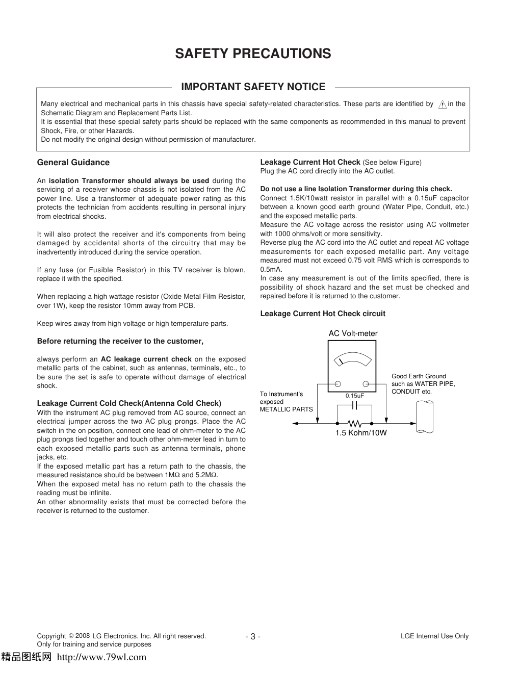
Leakage Current Hot Check (See below Figure)
Plug the AC cord directly into the AC outlet.
Do not use a line Isolation Transformer during this check.
Connect 1.5K/10watt resistor in parallel with a 0.15uF capacitor
between a known good earth ground (Water Pipe, Conduit, etc.)
and the exposed metallic parts.
Measure the AC voltage across the resistor using AC voltmeter
with 1000 ohms/volt or more sensitivity.
Reverse plug the AC cord into the AC outlet and repeat AC voltage
measurements for each exposed metallic part. Any voltage
measured must not exceed 0.75 volt RMS which is corresponds to
0.5mA.
In case any measurement is out of the limits specified, there is
possibility of shock hazard and the set must be checked and
repaired before it is returned to the customer.
Leakage Current Hot Check circuit
1.5 Kohm/10W
To Instrument’s
exposed
METALLIC PARTS
Good Earth Ground
such as WATER PIPE,
CONDUIT etc.
AC Volt-meter
IMPORTANT SAFETY NOTICE
0.15uF
精品图纸网 http://www.79wl.com
Copyright LG Electronics. Inc. All right reserved.
Only for training and service purposes
C 2008
LGE Internal Use Only
- 4 -
CAUTION: Before servicing receivers covered by this service
manual and its supplements and addenda, read and follow the
SAFETY PRECAUTIONS on page 3 of this publication.
NOTE: If unforeseen circumstances create conflict between the
following servicing precautions and any of the safety precautions on
page 3 of this publication, always follow the safety precautions.
Remember: Safety First.
General Servicing Precautions
1. Always unplug the receiver AC power cord from the AC power
source before;
a. Removing or reinstalling any component, circuit board
module or any other receiver assembly.
b. Disconnecting or reconnecting any receiver electrical plug or
other electrical connection.
c. Connecting a test substitute in parallel with an electrolytic
capacitor in the receiver.
CAUTION: A wrong part substitution or incorrect polarity
installation of electrolytic capacitors may result in an
explosion hazard.
2. Test high voltage only by measuring it with an appropriate high
voltage meter or other voltage measuring device (DVM,
FETVOM, etc) equipped with a suitable high voltage probe.
Do not test high voltage by "drawing an arc".
3. Do not spray chemicals on or near this receiver or any of its
assemblies.
4. Unless specified otherwise in this service manual, clean
electrical contacts only by applying the following mixture to the
contacts with a pipe cleaner, cotton-tipped stick or comparable
non-abrasive applicator; 10% (by volume) Acetone and 90% (by
volume) isopropyl alcohol (90%-99% strength)
CAUTION: This is a flammable mixture.
Unless specified otherwise in this service manual, lubrication of
contacts in not required.
5. Do not defeat any plug/socket B+ voltage interlocks with which
receivers covered by this service manual might be equipped.
6. Do not apply AC power to this instrument and/or any of its
electrical assemblies unless all solid-state device heat sinks are
correctly installed.
7. Always connect the test receiver ground lead to the receiver
chassis ground before connecting the test receiver positive
lead.
Always remove the test receiver ground lead last.
8. Use with this receiver only the test fixtures specified in this
service manual.
CAUTION: Do not connect the test fixture ground strap to any
heat sink in this receiver.
Electrostatically Sensitive (ES) Devices
Some semiconductor (solid-state) devices can be damaged easily
by static electricity. Such components commonly are called
Electrostatically Sensitive (ES) Devices. Examples of typical ES
devices are integrated circuits and some field-effect transistors and
semiconductor "chip" components. The following techniques
should be used to help reduce the incidence of component
damage caused by static by static electricity.
1. Immediately before handling any semiconductor component or
semiconductor-equipped assembly, drain off any electrostatic
charge on your body by touching a known earth ground.
Alternatively, obtain and wear a commercially available
discharging wrist strap device, which should be removed to
prevent potential shock reasons prior to applying power to the
unit under test.
2. After removing an electrical assembly equipped with ES
devices, place the assembly on a conductive surface such as
aluminum foil, to prevent electrostatic charge buildup or
exposure of the assembly.
3. Use only a grounded-tip soldering iron to solder or unsolder ES
devices.
4. Use only an anti-static type solder removal device. Some solder
removal devices not classified as "anti-static" can generate
electrical charges sufficient to damage ES devices.
5. Do not use freon-propelled chemicals. These can generate
electrical charges sufficient to damage ES devices.
6. Do not remove a replacement ES device from its protective
package until immediately before you are ready to install it.
(Most replacement ES devices are packaged with leads
electrically shorted together by conductive foam, aluminum foil
or comparable conductive material).
7. Immediately before removing the protective material from the
leads of a replacement ES device, touch the protective material
to the chassis or circuit assembly into which the device will be
installed.
CAUTION: Be sure no power is applied to the chassis or circuit,
and observe all other safety precautions.
8. Minimize bodily motions when handling unpackaged
replacement ES devices. (Otherwise harmless motion such as
the brushing together of your clothes fabric or the lifting of your
foot from a carpeted floor can generate static electricity
sufficient to damage an ES device.)
General Soldering Guidelines
1. Use a grounded-tip, low-wattage soldering iron and appropriate
tip size and shape that will maintain tip temperature within the
range or 500。F to 600。F.
2. Use an appropriate gauge of RMA resin-core solder composed
of 60 parts tin/40 parts lead.
3. Keep the soldering iron tip clean and well tinned.
4. Thoroughly clean the surfaces to be soldered. Use a mall wire-
bristle (0.5 inch, or 1.25cm) brush with a metal handle.
Do not use freon-propelled spray-on cleaners.
5. Use the following unsoldering technique
a. Allow the soldering iron tip to reach normal temperature.
(500。F to 600。F)
b. Heat the component lead until the solder melts.
c. Quickly draw the melted solder with an anti-static, suction-
type solder removal device or with solder braid.
CAUTION: Work quickly to avoid overheating the
circuitboard printed foil.
6. Use the following soldering technique.
a. Allow the soldering iron tip to reach a normal temperature
(500。F to 600。F)
b. First, hold the soldering iron tip and solder the strand against
the component lead until the solder melts.
c.
Quickly move the soldering iron tip to the junction of the
component lead and the printed circuit foil, and hold it there
only until the solder flows onto and around both the
component lead and the foil.
CAUTION: Work quickly to avoid overheating the circuit
board printed foil.
d.
Closely inspect the solder area and remove any excess or
splashed solder with a small wire-bristle brush.
SERVICING PRECAUTIONS
精品图纸网 http://www.79wl.com
Copyright LG Electronics. Inc. All right reserved.
Only for training and service purposes
C 2008
LGE Internal Use Only
- 5 -
IC Remove/Replacement
Some chassis circuit boards have slotted holes (oblong) through
which the IC leads are inserted and then bent flat against the
circuit foil. When holes are the slotted type, the following technique
should be used to remove and replace the IC. When working with
boards using the familiar round hole, use the standard technique
as outlined in paragraphs 5 and 6 above.
Removal
1. Desolder and straighten each IC lead in one operation by gently
prying up on the lead with the soldering iron tip as the solder
melts.
2. Draw away the melted solder with an anti-static suction-type
solder removal device (or with solder braid) before removing the
IC.
Replacement
1. Carefully insert the replacement IC in the circuit board.
2. Carefully bend each IC lead against the circuit foil pad and
solder it.
3. Clean the soldered areas with a small wire-bristle brush.
(It is not necessary to reapply acrylic coating to the areas).
"Small-Signal" Discrete Transistor
Removal/Replacement
1. Remove the defective transistor by clipping its leads as close as
possible to the component body.
2. Bend into a "U" shape the end of each of three leads remaining
on the circuit board.
3. Bend into a "U" shape the replacement transistor leads.
4. Connect the replacement transistor leads to the corresponding
leads extending from the circuit board and crimp the "U" with
long nose pliers to insure metal to metal contact then solder
each connection.
Power Output, Transistor Device
Removal/Replacement
1. Heat and remove all solder from around the transistor leads.
2. Remove the heat sink mounting screw (if so equipped).
3. Carefully remove the transistor from the heat sink of the circuit
board.
4. Insert new transistor in the circuit board.
5.
Solder each transistor lead, and clip off excess lead.
6. Replace heat sink.
Diode Removal/Replacement
1. Remove defective diode by clipping its leads as close as
possible to diode body.
2. Bend the two remaining leads perpendicular y to the circuit
board.
3. Observing diode polarity, wrap each lead of the new diode
around the corresponding lead on the circuit board.
4. Securely crimp each connection and solder it.
5.
Inspect (on the circuit board copper side) the solder joints of
the two "original" leads. If they are not shiny, reheat them and if
necessary, apply additional solder.
Fuse and Conventional Resistor
Removal/Replacement
1. Clip each fuse or resistor lead at top of the circuit board hollow
stake.
2. Securely crimp the leads of replacement component around
notch at stake top.
3. Solder the connections.
CAUTION: Maintain original spacing between the replaced
component and adjacent components and the circuit board to
prevent excessive component temperatures.
Circuit Board Foil Repair
Excessive heat applied to the copper foil of any printed circuit
board will weaken the adhesive that bonds the foil to the circuit
board causing the foil to separate from or "lift-off" the board. The
following guidelines and procedures should be followed whenever
this condition is encountered.
At IC Connections
To repair a defective copper pattern at IC connections use the
following procedure to install a jumper wire on the copper pattern
side of the circuit board. (Use this technique only on IC
connections).
1. Carefully remove the damaged copper pattern with a sharp
knife. (Remove only as much copper as absolutely necessary).
2. carefully scratch away the solder resist and acrylic coating (if
used) from the end of the remaining copper pattern.
3. Bend a small "U" in one end of a small gauge jumper wire and
carefully crimp it around the IC pin. Solder the IC connection.
4. Route the jumper wire along the path of the out-away copper
pattern and let it overlap the previously scraped end of the good
copper pattern. Solder the overlapped area and clip off any
excess jumper wire.
At Other Connections
Use the following technique to repair the defective copper pattern
at connections other than IC Pins. This technique involves the
installation of a jumper wire on the component side of the circuit
board.
1. Remove the defective copper pattern with a sharp knife.
Remove at least 1/4 inch of copper, to ensure that a hazardous
condition will not exist if the jumper wire opens.
2. Trace along the copper pattern from both sides of the pattern
break and locate the nearest component that is directly
connected to the affected copper pattern.
3. Connect insulated 20-gauge jumper wire from the lead of the
nearest component on one side of the pattern break to the lead
of the nearest component on the other side.
Carefully crimp and solder the connections.
CAUTION: Be sure the insulated jumper wire is dressed so the
it does not touch components or sharp edges.
精品图纸网 http://www.79wl.com
Copyright LG Electronics. Inc. All right reserved.
Only for training and service purposes
C 2008
LGE Internal Use Only
- 6 -
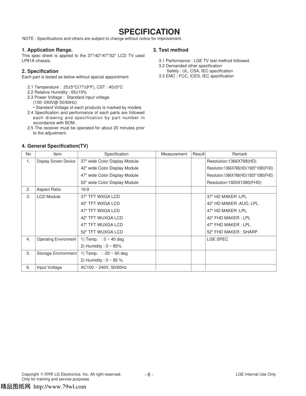
SPECIFICATION
NOTE : Specifications and others are subject to change without notice for improvement.
4. General Specification(TV)
No
Item
Specification
Measurement
Result
Remark
1.
Display Screen Device
37" wide Color Display Module
Resolution:1366X768(HD)
42" wide Color Display Module
Resolution:1366X768(HD)/1920*1080(FHD)
47" wide Color Display Module
Resolution:1366X768(HD)/1920*1080(FHD)
52" wide Color Display Module
Resolution:1920X1080(FHD)
2.
Aspect Ratio
16:9
3.
LCD Module
37" TFT WXGA LCD
37" HD MAKER :LPL
42" TFT WXGA LCD
42" HD MAKER :AUO, LPL
47" TFT WXGA LCD
47" HD MAKER :LPL
42" TFT WUXGA LCD
42" FHD MAKER : LPL
47" TFT WUXGA LCD
47" FHD MAKER : LPL
52" TFT WUXGA LCD
52" FHD MAKER : SHARP
4.
Operating Environment
1) Temp. : 0 ~ 40 deg
LGE SPEC
2) Humidity : 0 ~ 85%
5.
Storage Environment
1) Temp. : -20 ~ 60 deg
2) Humidity : 0 ~ 85 %
6.
Input Voltage
AC100 ~ 240V, 50/60Hz
1. Application Range.
This spec sheet is applied to the 37"/42"/47"/52" LCD TV used
LP81A chassis.
2. Specification
Each part is tested as below without special appointment
2.1 Temperature : 25±5°C(77±9°F), CST : 40±5°C
2.2 Relative Humidity : 65±10%
2.3 Power Voltage : Standard input voltage
(100~240V@ 50/60Hz)
• Standard Voltage of each products is marked by models
2.4 Specification and performance of each parts are followed
each drawing and specification by part number in
accordance with BOM .
2.5 The receiver must be operated for about 20 minutes prior
to the adjustment.
3. Test method
3.1 Performance : LGE TV test method followed.
3.2 Demanded other specification
Safety : UL, CSA, IEC specification
3.3 EMC : FCC, ICES, IEC specification
精品图纸网 http://www.79wl.com
Copyright LG Electronics. Inc. All right reserved.
Only for training and service purposes
C 2008
LGE Internal Use Only
- 7 -
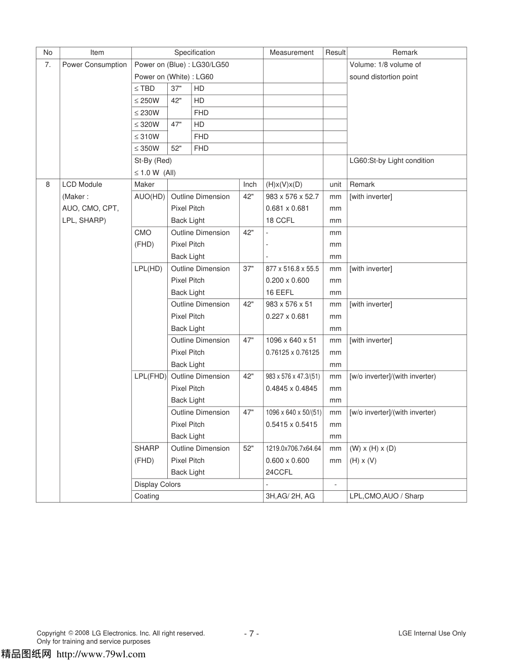
No
Item
Specification
Measurement
Result
Remark
7.
Power Consumption
Power on (Blue) : LG30/LG50
Volume: 1/8 volume of
Power on (White) : LG60
sound distortion point
≤ TBD
37"
HD
≤ 250W
42"
HD
≤ 230W
FHD
≤ 320W
47"
HD
≤ 310W
FHD
≤ 350W
52"
FHD
St-By (Red)
LG60:St-by Light condition
≤ 1.0 W (All)
8
LCD Module
Maker
Inch
(H)x(V)x(D)
unit
Remark
(Maker :
AUO(HD)
Outline Dimension
42"
983 x 576 x 52.7
mm
[with inverter]
AUO, CMO, CPT,
Pixel Pitch
0.681 x 0.681
mm
LPL, SHARP)
Back Light
18 CCFL
mm
CMO
Outline Dimension
42"
-
mm
(FHD)
Pixel Pitch
-
mm
Back Light
-
mm
LPL(HD)
Outline Dimension
37"
877 x 516.8 x 55.5
mm
[with inverter]
Pixel Pitch
0.200 x 0.600
mm
Back Light
16 EEFL
mm
Outline Dimension
42"
983 x 576 x 51
mm
[with inverter]
Pixel Pitch
0.227 x 0.681
mm
Back Light
mm
Outline Dimension
47"
1096 x 640 x 51
mm
[with inverter]
Pixel Pitch
0.76125 x 0.76125
mm
Back Light
mm
LPL(FHD) Outline Dimension
42"
983 x 576 x 47.3/(51)
mm
[w/o inverter]/(with inverter)
Pixel Pitch
0.4845 x 0.4845
mm
Back Light
mm
Outline Dimension
47"
1096 x 640 x 50/(51)
mm
[w/o inverter]/(with inverter)
Pixel Pitch
0.5415 x 0.5415
mm
Back Light
mm
SHARP
Outline Dimension
52"
1219.0x706.7x64.64
mm
(W) x (H) x (D)
(FHD)
Pixel Pitch
0.600 x 0.600
mm
(H) x (V)
Back Light
24CCFL
Display Colors
-
-
Coating
3H,AG/ 2H, AG
LPL,CMO,AUO / Sharp
精品图纸网 http://www.79wl.com
Copyright LG Electronics. Inc. All right reserved.
Only for training and service purposes
C 2008
LGE Internal Use Only
- 8 -
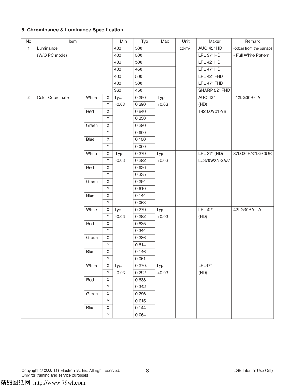
5. Chrominance & Luminance Specification
No
Item
Min
Typ
Max
Unit
Maker
Remark
1
Luminance
400
500
cd/m2
AUO 42" HD
-50cm from the surface
(W/O PC mode)
400
500
LPL 37" HD
- Full White Pattern
400
500
LPL 42" HD
400
450
LPL 47" HD
400
500
LPL 42" FHD
400
500
LPL 47" FHD
360
450
SHARP 52" FHD
2
Color Coordinate
White
X
Typ.
0.280
Typ.
AUO 42"
42LG30R-TA
Y
-0.03
0.290
+0.03
(HD)
Red
X
0.640
T420XW01-VB
Y
0.330
Green
X
0.290
Y
0.600
Blue
X
0.150
Y
0.060
White
X
Typ.
0.279
Typ.
LPL 37" (HD)
37LG30R/37LG60UR
Y
-0.03
0.292
+0.03
LC370WXN-SAA1
Red
X
0.636
Y
0.335
Green
X
0.284
Y
0.610
Blue
X
0.144
Y
0.063
White
X
Typ.
0.279
Typ.
LPL 42"
42LG30RA-TA
Y
-0.03
0.292
+0.03
(HD)
Red
X
0.635
Y
0.344
Green
X
0.286
Y
0.614
Blue
X
0.146
Y
0.061
White
X
Typ.
0.270.
Typ.
LPL47"
Y
-0.03
0.292
+0.03
(HD)
Red
X
0.638
Y
0.342
Green
X
0.296
Y
0.615
Blue
X
0.144
Y
0.064
精品图纸网 http://www.79wl.com
Copyright LG Electronics. Inc. All right reserved.
Only for training and service purposes
C 2008
LGE Internal Use Only
- 9 -
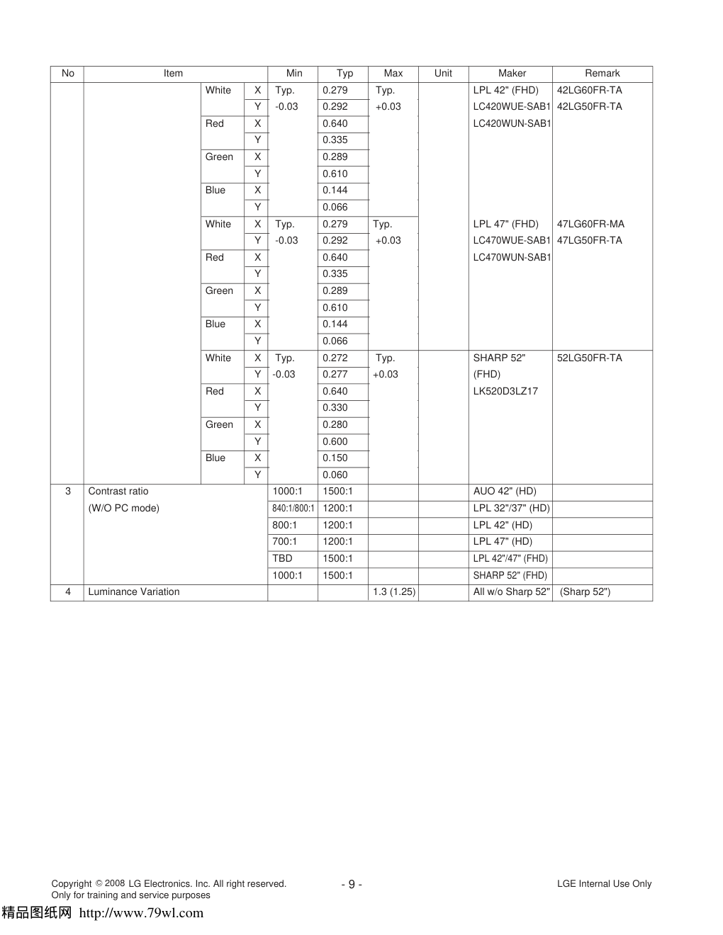
No
Item
Min
Typ
Max
Unit
Maker
Remark
White
X
Typ.
0.279
Typ.
LPL 42" (FHD)
42LG60FR-TA
Y
-0.03
0.292
+0.03
LC420WUE-SAB1 42LG50FR-TA
Red
X
0.640
LC420WUN-SAB1
Y
0.335
Green
X
0.289
Y
0.610
Blue
X
0.144
Y
0.066
White
X
Typ.
0.279
Typ.
LPL 47" (FHD)
47LG60FR-MA
Y
-0.03
0.292
+0.03
LC470WUE-SAB1 47LG50FR-TA
Red
X
0.640
LC470WUN-SAB1
Y
0.335
Green
X
0.289
Y
0.610
Blue
X
0.144
Y
0.066
White
X
Typ.
0.272
Typ.
SHARP 52"
52LG50FR-TA
Y
-0.03
0.277
+0.03
(FHD)
Red
X
0.640
LK520D3LZ17
Y
0.330
Green
X
0.280
Y
0.600
Blue
X
0.150
Y
0.060
3
Contrast ratio
1000:1
1500:1
AUO 42" (HD)
(W/O PC mode)
840:1/800:1 1200:1
LPL 32"/37" (HD)
800:1
1200:1
LPL 42" (HD)
700:1
1200:1
LPL 47" (HD)
TBD
1500:1
LPL 42"/47" (FHD)
1000:1
1500:1
SHARP 52" (FHD)
4
Luminance Variation
1.3 (1.25)
All w/o Sharp 52"
(Sharp 52")
精品图纸网 http://www.79wl.com
- 10 -
LGE Internal Use Only
Copyright LG Electronics. Inc. All right reserved.
Only for training and service purposes
C 2008
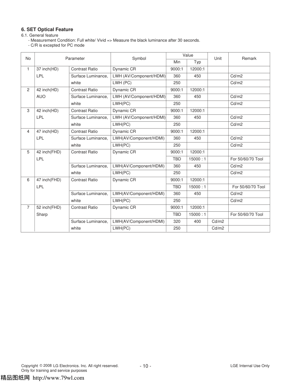
6. SET Optical Feature
6.1. General feature
- Measurement Condition: Full white/ Vivid => Measure the black luminance after 30 seconds.
- C/R is excepted for PC mode
No
Parameter
Symbol
Value
Unit
Remark
Min
Typ
1
37 inch(HD)
Contrast Ratio
Dynamic CR
9000:1
12000:1
LPL
Surface Luminance,
LWH (AV/Component/HDMI)
360
450
Cd/m2
white
LWH (PC)
250
Cd/m2
2
42 inch(HD)
Contrast Ratio
Dynamic CR
9000:1
12000:1
AUO
Surface Luminance,
LWH (AV/Component/HDMI)
360
450
Cd/m2
white
LWH(PC)
250
Cd/m2
3
42 inch(HD)
Contrast Ratio
Dynamic CR
9000:1
12000:1
LPL
Surface Luminance,
LWH (AV/Component/HDMI)
360
450
Cd/m2
white
LWH(PC)
250
Cd/m2
4
47 inch(HD)
Contrast Ratio
Dynamic CR
9000:1
12000:1
LPL
Surface Luminance,
LWH(AV/Component/HDMI)
360
450
Cd/m2
white
LWH(PC)
250
Cd/m2
5
42 inch(FHD)
Contrast Ratio
Dynamic CR
9000:1
12000:1
LPL
TBD
15000 : 1
For 50/60/70 Tool
Surface Luminance,
LWH(AV/Component/HDMI)
360
450
Cd/m2
white
LWH(PC)
250
Cd/m2
6
47 inch(FHD)
Contrast Ratio
Dynamic CR
9000:1
12000:1
LPL
TBD
15000 : 1
For 50/60/70 Tool
Surface Luminance,
LWH(AV/Component/HDMI)
360
450
Cd/m2
white
LWH(PC)
250
Cd/m2
7
52 inch(FHD)
Contrast Ratio
Dynamic CR
9000:1
12000:1
Sharp
TBD
15000 : 1
For 50/60/70 Tool
Surface Luminance,
LWH(AV/Component/HDMI)
320
400
Cd/m2
white
LWH(PC)
250
Cd/m2
精品图纸网 http://www.79wl.com
- 11 -
LGE Internal Use Only
Copyright LG Electronics. Inc. All right reserved.
Only for training and service purposes
C 2008
7. Component Video Input (Y, PB, PR)
No.
Specification
Remark
Resolution
H-freq(kHz)
V-freq(Hz)
Pixek clock
1.
720*480
15.73
59.94
13.500
SDTV, DVD 480I(525I)
2.
720*480
15.75
60.00
13.514
SDTV, DVD 480I(525I)
3.
720*576
15.625
50.00
13.500
SDTV, DVD 576I(625I) 50Hz
4.
720*480
31.47
59.94
27.000
SDTV 480P
5.
720*480
31.50
60.00
27.027
SDTV 480P
6.
720*576
31.25
50.00
27.000
SDTV 576P 50Hz
7.
1280*720
44.96
59.94
74.176
HDTV 720P
8.
1280*720
45.00
60.00
74.250
HDTV 720P
9.
1280*720
37.50
50.00
74.25
HDTV 720P 50Hz
10.
1920*1080
28.125
50.00
74.250
HDTV 1080I 50Hz,
11.
1920*1080
33.72
59.94
74.176
HDTV 1080I
12.
1920*1080
33.75
60.00
74.25
HDTV 1080I
13.
1920*1080
56.25
50
148.5
HDTV 1080P
14
1920*1080
67.432
59.94
148.350
HDTV 1080P
15
1920*1080
67.5
60.00
148.5
HDTV 1080P
8. RGB Input (Analog PC)
No.
Resolution
H-freq(kHz)
V-freq(Hz)
Pixel clock(MHz)
Proposed
Remark
1.
640*350
31.468
70.80
25.17
EGA
2
720*400
31.469
70.08
28.32
DOS
3.
640*480
31.469
59.94
25.17
VESA(VGA)
4
800*600
37.879
60.31
40
VESA(SVGA)
5
1024*768
48.363
60
65
VESA(XGA)
6
1280*768
47.776
59.87
79.5
VESA(WXGA)
7
1360*768
47.72
59.799
84.75
VESA(WXGA)
8
1366*768
47.7
60
84.62
VESA(WXGA)
9
1280*1024
63.668
59.895
109.00
SXGA
Only FHD
10
1400*1050
65.317
59.978
121.75
SXGA
Only FHD
11
1600*1200
74.537
59.869
161.00
UXGA
Only FHD
12
1920*1080
66.587
59.934
138.50
WUXGA (Reduced Blanking)
Only FHD
精品图纸网 http://www.79wl.com
- 12 -
LGE Internal Use Only
Copyright LG Electronics. Inc. All right reserved.
Only for training and service purposes
C 2008
9. HDMI Input (PC-Spec. out but display correctly at only HDMI/DVI IN 1 via DVI to HDMI cable)
No.
Resolution
H-freq(kHz)
V-freq(Hz)
Pixel clock(MHz)
Proposed
Remark
1.
720x400
31.468
70.08
28.32
2.
640x480
31.469
59.94
25.17
VESA(VGA)
3.
800x600
37.879
60.31
40.00
VESA(SVGA)
4
1024x768
48.363
60.00
65.00
VESA(XGA)
5
1280x768
47.776
59.87
79.5
VESA(WXGA)
6
1360x768
47.72
59.799
84.62
VESA(WXGA)
7
1366x768
47.7
60
84.62
VESA(WXGA)
8
1280x1024
63.595
60.0
108.875
SXGA
Only FHD
9
1400x1050
65.160
60.0
122.50
SXGA
Only FHD
10
1600x1200
74.077
60.0
130.375
UXGA
Only FHD
11
1920x1080
66.647
59.988
138.625
WUXGA
Only FHD
10. HDMI input ( DTV )
No.
Resolution
H-freq(kHz)
V-freq(Hz)
Pixel clock(MHz)
Proposed
Remark
1
720*480
31.47
59.94
27
SDTV 480P
Support(not spec)
2
720*480
31.5
60
27.027
SDTV 480P
support(not spec)
3
720*576
31.25
50
27
SDTV 576P
support(not spec)
4
1280*720
44.96
59.94
74.176
HDTV 720P
5
1280*720
45
60
74.25
HDTV 720P
6
1280*720
37.5
50
74.25
HDTV 720P
7
1920*1080
28.125
50
74.25
HDTV 1080I
8
1920*1080
33.72
59.94
74.176
HDTV 1080I
9
1920*1080
33.75
60
74.25
HDTV 1080I
10
1920*1080
56.25
50
148.5
HDTV 1080P
11
1920*1080
67.432
59.94
148.350
HDTV 1080P
12
1920*1080
67.5
60.00
148.5
HDTV 1080P
13
1920*1080
27
24
74.25
HDTV 1080P
14
1920*1080
33.75
30
74.25
HDTV 1080P
精品图纸网 http://www.79wl.com
Copyright LG Electronics. Inc. All right reserved.
Only for training and service purposes
C 2008
LGE Internal Use Only
- 13 -
ADJUSTMENT INSTRUCTION
1. Application Range
These instructions are applied to all of the LCD TV, LP81A
Chassis.
2. Notice
2.1 Because this is not a hot chassis, it is not necessary to
use an isolation transformer. However, the use of
isolation transformer will help protect test instrument.
2.2 Adjustment must be done in the correct order.
2.3 The adjustment must be performed in the circumstance of
25±5°C of temperature and 65±10% of relative humidity if
there is no specific designation.
2.4 The input voltage of the receiver must keep 100~220V,
50/60Hz.
2.5 Before adjustment, execute Heat-Run for 15 minutes at
RF no signal.
3. Adjustment items
3.1 PCB assembly adjustment items
Download the MSTAR main software (IC801, Mstar ISP
Utility)
3.2 SET assembly adjustment items
DDC Data input.
Adjustment of White Balance.
Factoring Option Data input
4. PCB assembly adjustment method
(Using MSTAR Download program)
4.1 S/W program download
4.1.1 Preliminary steps
(1) Download method 1 (PCB Assy)
- HD
- FHD
(2) Connect the download jig to D-sub jack
精品图纸网 http://www.79wl.com
4.1.2 Download steps
(1) Execute ‘ISP Tool’ program in PC, then a main window
will be opened
(2) Click the connect button and confirm "Dialog Box".
(3) Click the Config button and Change speed
E2PROM Device setting : over the 350Khz
(4) Read and write bin file
Click "(1)Read" tab, and then load download
file(XXXX.bin) by clicking "Read".
(5).Click "Auto(2)" tab and set as below
(6).click "Run(3)".
(7).After downloading, check "OK(4)" message.
# USB DOWNLOAD
1. Put the USB Stick to the USB socket
2. Automatically detecting update file in USB Stick
- 14 -
LGE Internal Use Only
Copyright LG Electronics. Inc. All right reserved.
Only for training and service purposes
C 2008
Double click
精品图纸网 http://www.79wl.com
3. Select "Start" Button and press "ok" button
Updating is staring.
4. Finishing the version updating, you have to put out USB stick
and "AC Power" off
5. After putting "AC Power" on and check updated version on
your TV
4.2 ADC Process
O Required Equipments
- Remote controller for adjustment
- MSPG-925F Pattern Generator
4.2.1 Method of Auto RGB Color Balance
- Convert to RGB PC in Input-source
- Input the PC 1024x768 @ 60Hz 1/2 Black & White
Pattern(MSPG-925F model:60, pattern:54) into RGB
- Adjust by commanding AUTO_COLOR_ADJUST(0xF1)
0x00 0x02 instruction.
4.2.1.1 Confirmation
- We confirm whether "0xF3 (offset), 0xF4 (gain)" address of
EEPROM "0xBC" is "0xAA" or not.
- If "0xF3", "0xF4" address of EEPROM "0xBC" isn’t "0xAA",
we adjust once more
- We can confirm the ADC values from "0x06~0x0B"
addresses in a page "0xBC"
*Manual ADC process using Service Remocon. After enter
Service Mode by pushing "ADJ" key, execute "Auto-RGB"
by pushing "_" key at "Auto-RGB".
4.2.2 Component input ADC
4.2.2.1 Component Gain/Offset Adjustment7
- Convert to Component in Input-source
- Input the Component ( Which has 720p@60Hz YPbPr
signal : 100% Color Bar (MSPG-925F Model : 217 / Pattern:
65 ) into Component.
- Adjust by commanding AUTO_COLOR_ADJUST (0xF1)
0x00 0x02 instruction
4.2.2.2 Confirmation
- We confirm whether "0xF3 (offset), 0xF4 (gain)" address of
EEPROM "0xBC" is "0xAA" or not.
- If "0xF3", "0xF4" address of EEPROM "0xBC" isn’t "0xAA",
we adjust once more
- We can confirm the ADC values from "0x06~0x0B"
addresses in a page "0xBC"
*Manual ADC process using Service Remocon. After enter
Service Mode by pushing "ADJ" key, execute "Auto-RGB"
by pushing "_" key at "Auto-RGB".
- 15 -
LGE Internal Use Only
Copyright LG Electronics. Inc. All right reserved.
Only for training and service purposes
C 2008
精品图纸网 http://www.79wl.com
5. Adjusting the White Balance
5.1 Purpose and Principle for adjustment of the
color temperature
- Purpose : Adjust the color temperature to reduce the
deviation of the module color temperature.
- Principle : To adjust the white balance without the
saturation,
(Fix the one of R/G/B gain to C0 and decrease the others.)
5.2 Adjustment mode : Two modes of Cool and Warm
(Medium data is automatically calibrated by the
Cool data)
O Required Equipments
- Remote controller for adjustment
- Color Analyzer : CA100+ or CA-210 or same product
LCD TV( ch : 9 ),
- Auto W/B adjustment instrument(only for Auto adjustment)
5.3 Connecting diagram of equipment for
measuring (For Automatic Adjustment)
(1) Enter the adjustment mode of DDC
- Set command delay time : 50ms
- Enter the DDC adjustment mode at the same time heat-
- Maintain the DDC adjustment mode with same condition
of Heat-run
-> Maintain after AC off/on in status of Heat-run pattern
display)
(2) Release the DDC adjustment mode
- Release the adjust mode after AC off/on or std-by off/on
in status of finishing the Hear-run mode
- Release the Adjust mode when receiving the aging off
command(F3 00 00) from adjustment equipment
- Need to transmit the aging off command to TV set after
finishing the adjustment.
- Check DDC adjust mode release by exit key and
release DDC adjust mode
(3) Enter the adjust mode of white balance
- Enter the white balance adjustment mode with aging
command(F3, 00, FF)
* Luminance min value is 200cd/ß≥ in the cool mode( For
LCD)
6. Adjustment of White Balance
• Adjustment mode : Two modes (Cool and Warm)
(Medium data is automatically calibrated by the Cool data)
• Color analyzer(CA100+, CA210) should be used in the
calibrated ch by CS-1000
(LCD : CH9, PDP : CH10)
• Operate the zero-calibration of the CA100+ or CA-210, then
stick sensor to the module when adjusting.
• For manual adjustment, it is also possible by the following
sequence.
1) Select white pattern of heat-run by pressing "POWER ON"
key on remote control for adjustment then operate heat run
longer than 15 minutes.
(If not executed this step, the condition for W/B may be
different.)
2) Push "Exit" key.
3) Change to the AV mode by remote control.(Push front-AV
or Input key)
4) Input external pattern(85% white pattern)
5) Push the ADJ key two times (entering White Balance
mode)
6) Stick the sensor to the center of the screen and select
each items (Red/Green/Blue Gain and Offset) using
/
(CH +/-) key on R/C..
7) Adjust R/ G/ B Gain using
/
(VOL+/-) key on R/C.
8) Adjust two modes (Cool and Warm)
(Fix the one of R/G/B and change the others)
9) When adjustment is completed, Exit adjustment mode
using EXIT key on R/C.
- 16 -
LGE Internal Use Only
Copyright LG Electronics. Inc. All right reserved.
Only for training and service purposes
C 2008
精品图纸网 http://www.79wl.com
TROUBLE SHOOTING
- 17 -
LGE Internal Use Only
Copyright LG Electronics. Inc. All right reserved.
Only for training and service purposes
C 2008
1) Symptom
1) It is not discharged minutely from the module.
2) Light does not come into the front LED.
2) Check process
1. No power
No
Yes
Is plug in
Power cord inserted?
After all cables connect is
removed to PSU.
The AC voltage marking is
authorized on manual.
When ST-By 5V is not operated.
replace PSU.
Plug in power cord
No
Yes
Is the Line Filter
and PSU connected?
Connect a cable to SC100
No
Yes
Is the fuse of
PSU normal?
F101
Replace the fuse.
No
Yes
Is it connected that
PSU and P1100 in
Main Board
Connect a cable P1100
精品图纸网 http://www.79wl.com
Copyright LG Electronics. Inc. All right reserved.
Only for training and service purposes
C 2008
- 18 -
LGE Internal Use Only
1) Symptom
1) No OSD and image occur at screen.
2) It maintains the condition where the front LED is green
.
2) Check process
2. No Raster
No
No
No
No
No
Yes
Yes
Yes
CN700(PDP/LCD)
Replace the VSC.
Does mimute
discharge a Module?
Is the Link cable
normal?
Is the IC801’s
output normal?
Check the LCD Module
Reconnect the
Panel line cable
(HD:P403, FHD:402)
Is the inverter
/VaVs on?
Is output the normality
Low/High voltage
except Stand-by 5V?
Replace the
Power board
精品图纸网 http://www.79wl.com
Copyright LG Electronics. Inc. All right reserved.
Only for training and service purposes
C 2008
- 19 -
LGE Internal Use Only
1) Check process
3. Unusual display from RF mode.
No
Yes
Yes
No
No
Is Video output of the
Tuner normal?
(Check TU500_Pin13)
Is the
Input voltage normal?
(Check Pin3)
Block A
Is the I2C communication normal?
(Check Pin9, Pin10)
No
Yes
Is the LVDS
cable connected well?
Change the IC(IC801)
Check the power
Cable inserts well
Check the Tuner
精品图纸网 http://www.79wl.com
Copyright LG Electronics. Inc. All right reserved.
Only for training and service purposes
C 2008
- 20 -
LGE Internal Use Only
4. Unusual display from rear AV mode
.
5. Unusual display from Side AV mode.
6. Unusual display from Side S-Video mode.
7. Unusual display from component 1 mode.
8. Unusual display from component 2 mode.
9. Unusual display from RGB mode.
No
Yes
Is video input of the
A/V Jack normal?
(Check R8044)
Same as Block A
Same as Block A
Same as Block A
Check the input source.
Check the input source.
Check the input source.
Check the input source.
Change IC801
Change IC801
Change IC801
Is Video input of the
Comp1 jack normal?
(Check R8011,8012,8013)
Is Video input of the
Comp2 jack normal?
(Check R8030,8032,8033)
Is Video input of the
Comp2 jack normal?
(Check R8035,8037,8039)
Check the input source.
Check the input source.
Is video input of the
Side A/V Jack normal?
(Check R8043)
Is video input of the
S-Video Jack normal?
(Check R8041,8042)
No
Yes
No
Yes
No
Yes
No
Yes
No
Yes
精品图纸网 http://www.79wl.com
- 21 -
LGE Internal Use Only
Copyright LG Electronics. Inc. All right reserved.
Only for training and service purposes
C 2008
10-1 Symptom
1) LED is green.
2) Screen display but sound is not output.
10. No Sound
10-2 Check process
All input(mode)
is no sound.
Only HDMI is
no sound
Only AV/
COM2/PC input is
no sound.
Only External speaker
is no sound
Check the Tuner In/Out.
Check the signal after
IC600 refer to circuit
diagram
Is the output of
IC600 normal?
Download the EDID data.
No
No
No
No
No
Yes
Yes
Yes
Yes
Menu?
Normal
Normal
No
No
No
No
Yes
Yes
Yes
Yes
Replace
IC600
Is the speaker
on it men?
Set on speaker
in menu
Check the
Speaker cable
Replace
IC801
Replace
IC601
Is the speaker
cable normal?
IC801 operate
normal?
IC 601 operate
normal?
Replace Main B/D
精品图纸网 http://www.79wl.com
Copyright LG Electronics. Inc. All right reserved.
Only for training and service purposes
C 2008
LGE Internal Use Only
- 22 -
BLOCK DIAGRAM
AV1 in
SideAV in
(AV2 in)
Comp1 in
Comp2 in
RGB in
(D/L)
CVBS IN
Y/Pb/Pr IN
R/G/B/HS/VS IN
CVBS IN
LINE OUT
LINE
IN
AMP_MUTE
RS-232C
Rx/Tx MX3232
RF
(Tuner)
PC Audio
in
DISPLAY MODULE
EDID NVM
EDID NVM
HDMI1
HDMI2
HDMI3
USB
TMDS351PAG
HDMI MUX
Zoran
VADDIS-966XD
MPEG Decoder
DDR MEM
DDR MEM
SERIAL
FLASH
Mstar
Romeo
LGE6891CD
TW9910
Sub Decoder
NTP3000A
Digital
Audio AMP
MAIN NVM
MC74HC4066
Audio SW
LM324
X4 AMP
SERIAL
FLASH
BD2041
Protect IC
EDID NVM
DDC/HDP/CEC
TMDS(HDMI in)
DDC/HPD/CEC
TMDS(HDMI in)
TMDS(HDMI in)
USB(AV I/O, Data I/O)
+5V
CVBS
OUT
656 IN
SW_RESE
T
PART_I2
C
PART_I2C
SW_RESE
T
I2S OUT
LVDS
MPEG RX/TX
MPEG RESET
I2S IN
656 IN
TMDS(HDMI in)
DDC/HPD/CEC
DDC/HPD/CEC
[CEC not through HDMI MUX, direct JACK to MAIN IC]
DDC
DDC
DDC
UART_Rx/Tx
AUDIO_SW
LINE
IN
LINE
IN
LINE
IN
Y/Pb/Pr IN
LINE
IN
Y/C IN
LINE
IN
EDID NVM
ROM_I2C
DSUB_DDC
x0.55
x0.55
x0.55
x0.55
S_VIDEO_DET
LINE_MUTE
LINE OUT
x4
x0.55
LINE
IN
CVBS IN
SIF IN
TUNER_I2C
PART_I2C
HDMI_SEL
(Option)
(Option)
(Option)
Spk Out
1W(Mono)
SW_RESET
TPA3107D
Audio Amp
精品图纸网 http://www.79wl.com
Copyright LG Electronics. Inc. All right reserved.
Only for training and service purposes
C 2008
LGE Internal Use Only
- 23 -
EXPLODED VIEW
801
803
805
806
804
802
550
830
540
821
400
521
530
522
300
120
122
510
500
901
900
121
200
精品图纸网 http://www.79wl.com
精品图纸网 http://www.79wl.com
Copyright LG Electronics. Inc. All right reserved.
Only for training and service purposes
C 2008
LGE Internal Use Only
THE SYMBOL MARK OF THIS SCHEMETIC DIAGRAM INCORPORATES
SPECIAL FEATURES IMPORTANT FOR PROTECTION FROM X-RADIATION.
FILRE AND ELECTRICAL SHOCK HAZARDS, WHEN SERVICING IF IS
ESSENTIAL THAT ONLY MANUFATURES SPECFIED PARTS BE USED FOR
THE CRITICAL COMPONENTS IN THE SYMBOL MARK OF THE SCHEMETIC.
220K
R133
75
R121
75
R111
SD05
D105
220K
R108
COMP1_R
COMP1_Pb
PC_AUD_R
CDS3C05GTA
5.6V
D122
COMP1_Y
SD05
30V
D117
75
R123
5.6V
D103
COMP2_Pr
CDS3C05GTA
5.6V
D123
PPJ209-02
JK100
4A[GN]CONTACT
2A [GN]1P_CAN
3A [GN]O_SPRING
2B [BL]1P_CAN
5B [BL]C_LUG_L
2C [RD]1P_CAN1
5C [RD]C_LUG_L
2D [WH]1P_CAN
5D[WH]C_LUG_L
2E [RD]1P_CAN2
4E[RD]CONTACT
3E [RD]O_SPRING
SD05
D106
5.6V
D104
COMP2_L
220K
R119
COMP1_Pr
COMP1_L
75
R122
75
R110
220K
R106
220K
R120
COMP2_Pb
PPJ209-02
JK101
4A
[GN]CONTACT
2A
[GN]1P_CAN
3A
[GN]O_SPRING
2B
[BL]1P_CAN
5B
[BL]C_LUG_L
2C
[RD]1P_CAN1
5C
[RD]C_LUG_L
2D
[WH]1P_CAN
5D
[WH]C_LUG_L
2E
[RD]1P_CAN2
4E
[RD]CONTACT
3E
[RD]O_SPRING
30V
D119
SD05
1000-ohm
L100
PC_AUD_L
COMP2_R
220K
R132
SD05
30V
D118
1000-ohm
L101
SD05
D107
COMP2_Y
75
R109
5.6V
D115
5.6V
D116
10K
R136
10K
R143
10K
R144
12K
R142
12K
R145
12K
R137
10K
R134
12K
R135
10K
R138
10K
R140
12K
R139
12K
R141
68
R114
DSUB_SCL
75
R116
CDS3C30GTH
30V
D112
DSUB_SDA
+5V_ST
CDS3C30GTH
30V
D110
100
R125
+5V_MULTI
75
R117
DSUB_SDA
DSUB_SCL
0.1uF
C100
PC_G
CDS3C30GTH
30V
D114
0.1uF
C102
75
R118
4.7K
R112
68
R115
0.1uF
C101
PC_R
PC_B
PC_VS
68pF
C103
PC_HS
0.1uF
C105
4.7K
R113
68pF
C104
CDS3C30GTH
30V
D113
100
R124
100
R128
4.7K
R150
READY
+5V_ST
100
R129
100
R130
0.1uF
C110
0.1uF
C106
100
R131
OPT
C111
TXD
0.1uF
C108
0.1uF
C109
OPT
C112
RXD
CDS3C30GTH
30V
D121
0.1uF
C107
4.7K
R151
READY
+3.3V_MST
CDS3C30GTH
30V
D120
+5V_ST
ENKMC2837-T112
D109
A
AC
C
ENKMC2837-T112
D111
A
AC
C
ENKMC2837-T112
D108
A
AC
C
MAX3232CDR
IC101
RS232C
3
C1-
2
V+
4
C2+
1
C1+
6
V-
5
C2-
7
DOUT2
8
RIN2
9
ROUT2
10
DIN2
11
DIN1
12
ROUT1
13
RIN1
14
DOUT1
15
GND
16
VCC
PEJ024-01
JK102
6B
T_TERMINAL2
8
SHIELD_PLATE
7B
B_TERMINAL2
5
T_SPRING
4
R_SPRING
7A
B_TERMINAL1
6A
T_TERMINAL1
3
E_SPRING
IR_OUT
4.7K
R127
4.7K
R126
6630TGA004K
KCN-DS-1-0089
JK104
1
RED
2
GREEN
3
BLUE
4
GND_1
5
DDC_GND
6
RED_GND
7
GREEN_GND
8
BLUE_GND
9
NC
10
SYNC_GND
11
GND_2
12
DDC_DATA
13
H_SYNC
14
V_SYNC
15
DDC_CLOCK
16 SHILED
KCN-DS-1-0088
JK103
1
2
3
4
5
6
7
8
9
10
AT24C02BN-10SU-1.8
IC100
3
A2
2
A1
4
GND
1
A0
5
SDA
6
SCL
7
WP
8
VCC
1000pF
READY
C113
0
R146
1000pF
READY
C114
0
R147
1000pF
READY
C115
0
R148
1000pF
READY
C116
0
R149
COMPONENT2
SDC 15 applying check
PC SOUND
COMPONENT1
INPUT1 : COMP1/2,RS232C,PC
PC
RS-232C
*ONLY LG30
1.24C02-SUB:0IMMRAL014D
**MULTI ITEM
2.ENKMC2837-SUB:0DS226009AA
(KDS226)
SUB : 0IMCRSG010A(STM)
MAIN : EAN41348201(TI)
*RS232C TX
THE SYMBOL MARK OF THIS SCHEMETIC DIAGRAM INCORPORATES
SPECIAL FEATURES IMPORTANT FOR PROTECTION FROM X-RADIATION.
FILRE AND ELECTRICAL SHOCK HAZARDS, WHEN SERVICING IF IS
ESSENTIAL THAT ONLY MANUFATURES SPECFIED PARTS BE USED FOR
THE CRITICAL COMPONENTS IN THE SYMBOL MARK OF THE SCHEMETIC.
5.6V
D216
220K
R244
SIDE_RIN
75
R241
SD05
D214
SIDE_V
220K
R242
SIDE_LIN
5.6V
D215
75
R245
SIDE_Y
75
R246
SIDE_C
SD05
D217
SD05
D218
S_VIDEO_DET
SD05
D219
12K
R248
12K
R250
10K
R247
10K
R249
OPT
C210
READY
PPJ218-01
JK204
5C
[RD]CONTACT
2C
[RD]U_CAN
4C
[RD]O_SPRING
2B
[WH]U_CAN
3B
[WH]C_LUG
2A
[YL]U_CAN
5A
[YL]CONTACT
4A
[YL]O_SPRING
PSJ015-02
JK205
5
O_SPRING
4A
C_LUG_L_1
4B
C_LUG_S_1
4C
C_LUG_L_2
4D
C_LUG_S_2
3
GROUND
7
SHIELD
0.1uF
16V
READY
C213
0
R252
0
R251
100pF
50V
READY
C214
100pF
50V
READY
C215
75
R208
100pF
50V
C212
OPT
0
R210
470K
R229
OPT
RT1C3904-T112
Q203
OPT
E
B
C
SD05
D201
SPK_R-_HOTEL
5.6V
D208
OPT
470K
R230
OPT
100pF
50V
C211
OPT
PPJ148-10
JK200
4A
[RD]O_SPRING
2A
[RD]1P_CAN
5A
[RD]CONTACT
2
[WH]1P_CAN
3
[WH]C_LUG_L
2B
[YL]1P_CAN
4B
[YL]O_SPRING
5B
[YL]CONTACT
12K
R219
220K
R212
0
R214
10K
R218
0
R222
100pF
50V
C216
OPT
5.6V
D209
OPT
MNT_ROUT
MNT_LOUT
0
R211
OPT
C207
CVBS_RIN
12K
R221
1K
R236
OPT
CVBS_LIN
AUDIO_R
10K
R220
10uF
16V
C209
MUTE_LINE
PPJ200-01
JK201
2
1
3
4
5
1K
R237
OPT
220K
R209
SPK_R+_HOTEL
100pF
50V
C217
OPT
10uF
16V
C208
OPT
CVBS_VIN
0
R213
5.6V
D202
RT1C3904-T112
Q202
OPT
E
B
C
5.6V
D204
0
R223
INPUT2 : CVBS,SIDE AV
SIDE AV
POP NOISE
CVBS
THE SYMBOL MARK OF THIS SCHEMETIC DIAGRAM INCORPORATES
SPECIAL FEATURES IMPORTANT FOR PROTECTION FROM X-RADIATION.
FILRE AND ELECTRICAL SHOCK HAZARDS, WHEN SERVICING IF IS
ESSENTIAL THAT ONLY MANUFATURES SPECFIED PARTS BE USED FOR
THE CRITICAL COMPONENTS IN THE SYMBOL MARK OF THE SCHEMETIC.
TMDS3_RX2-
TMDS3_RXC-
HPD_S/W_2
TMDS2_RXC-
1K
R319
+5V_HDMI_2
HDMI_SEL1
TMDS3_RXC-
HDMI_C-
HDMI_SCL
HDMI_0-
10K
R351
HPD_MST_2
TMDS3_RX0+
TMDS2_RX2-
HDMI_C+
TMDS1_RX0+
+5V_HDMI_3
4.7K
R362
CEC_C
DDC_SCL1
CEC
TMDS1_RX1-
HDMI1_5V_DET
TMDS2_RX1+
HDMI3_5V_DET
TMDS2_RXC-
TMDS2_RXC+
0.01uF
C310
1K
R344
SIDE_HDMI
10K
R300
0.01uF
C315
HDMI_0+
+3.3V_MULTI_MST
1K
R310
+3.3V
CEC
DDC_SDA2
0.01uF
C314
TMDS3_RX2+
TMDS1_RXC-
HDMI_1-
0.01uF
C316
10K
R328
HPD_S/W_1
TMDS2_RX0+
TMDS2_RX0+
0.01uF
C308
TMDS3_RX0-
HDMI_2-
HPD_S/W_3
TMDS3_RX0-
TMDS3_RX1+
HDMI2_5V_DET
10K
R324
0
READY
R369
TMDS3_RXC+
DDC_SCL3
TMDS1_RXC+
+3.3V_MULTI_MST
+5V_HDMI_2
HPD_S/W_2
HPD_MST_1
CEC
BSS83
Q306
S
B
D
G
10K
R335
SIDE_HDMI
TMDS1_RX1+
TMDS3_RX1-
TMDS2_RXC+
0
R370
READY
TMDS1_RX2+
4.7K
R375
READY
0
R373
TMDS2_RX1+
TMDS1_RX0-
+3.3V_HDMI_SW
+5V_ST
4.7K
R361
0
R356
TMDS2_RX2-
+5V_HDMI_1
TMDS3_RX2-
TMDS3_RX2+
0
R358
HDMI_1+
0.01uF
50V
READY
C307
TMDS2_RX0-
TMDS2_RX0-
TMDS1_RX1-
4.7K
R374
KDS184S
KDS184
D300
A2
C
A1
10K
R329
TMDS2_RX1-
TMDS3_RX0+
0.01uF
C311
0.01uF
C312
TMDS1_RX2-
+5V_HDMI_3
TMDS3_RX1-
TMDS2_RX2+
HDMI_2+
HDMI_SEL2
TMDS1_RX2+
+5V_HDMI_1
10K
R352
TMDS3_RX1+
0.01uF
C309
0
R357
TMDS1_RXC-
0
R355
+5V_ST
TMDS3_RXC+
+5V_HDMI_3
+5V_ST
10K
R301
TMDS1_RX2-
+3.3V_HDMI_SW
+5V_HDMI_1
TMDS1_RX0-
TMDS2_RX1-
TMDS1_RX1+
HPD_S/W_1
0
R368
READY
10K
R325
0
R347
CEC
HDMI_SDA
DDC_SCL2
+5V_HDMI_2
HPD_S/W_3
TMDS1_RX0+
TMDS2_RX2+
0
R345
KDS184S
KDS184
D303
A2
C
A1
DDC_SDA1
0
R346
TMDS1_RXC+
CDS3C30GTH
30V
D302
READY
HPD_MST_3
DDC_SDA3
KDS184S
KDS184
D301
A2
C
A1
0
R350
47K
R330
47K
R331
47K
R326
47K
R327
47K
R354
47K
R353
0
READY
R365
0
READY
R376
MMBD301LT1G
30V
D304
A
C
DDC_SDA2
DDC_SCL2
DDC_SDA1
DDC_SCL1
DDC_SDA3
DDC_SCL3
TMDS351PAG
IC302
1
SDA3
2
SCL3
3
GND_1
4
B31
5
A31
6
VCC_1
7
B32
8
A32
9
GND_2
10
B33
11
A33
12
VCC_2
13
B34
14
A34
15
GND_3
16
VSADJ
17
Y4
18
Z4
19
VCC_3
20
Y3
21
Z3
22
GND_4
23
Y2
24
Z2
25
VCC_4
26
Y1
27
Z1
28
GND_5
29
SCL_SINK
30
SDA_SINK
31
HPD_SINK
32
S1
33
S2
34
EQ
35
HPD1
36
SDA1
37
SCL1
38
B11
39
A11
40
VCC_5
41
B12
42
A12
43
GND_6
44
B13
45
A13
46
VCC_6
47
B14
48
A14
49
VDD
50
HPD2
51
SDA2
52
SCL2
53
B21
54
A21
55
VCC_7
56
B22
57
A22
58
GND_7
59
B23
60
A23
61
VCC_8
62
B24
63
A24
64
HPD3
0
READY
R383
0.01uF
50V
C301
0.01uF
50V
C313
0.01uF
50V
C300
51K
R333
30K
R334
READY
4.7K
1%
R372
JP1115
JP1116
JP1117
JP1118
JP1119
JP1120
2SC3875S
RT1C3904-T112
Q300
E
B
C
2SC3875S
RT1C3904-T112
Q301
E
B
C
2SC3875S
Q307
SIDE_HDMI
E
B
C
DC1R019NBH
JK303
SIDE_HDMI
14 NC
13 CEC
5 DATA1_SHIELD
20
JACK_GND
12
CLK-
11 CLK_SHIELD
2 DATA2_SHIELD
19 HPD
18+5V_POWER
10 CLK+
4 DATA1+
1 DATA2+
17DDC/CEC_GND
9 DATA0-
8 DATA0_SHIELD
3 DATA2-
16 SDA
7 DATA0+
6 DATA1-
15 SCL
47K
R371
+3.3V
200
R332
QJ41193-FEE2-7F
JK302
1 DATA2+
2 DATA2_SHIELD
3 DATA2-
4 DATA1+
5 DATA1_SHIELD
6 DATA1-
7 DATA0+
8 DATA0_SHIELD
9
DATA0-
10 CLK+
11 CLK_SHIELD
12
CLK-
13 CEC
14 NC
15
SCL
16 SDA
17 DDC/CEC_GND
18 +5V_POWER
19 HPD
20 JACK_GND
21
.
22
.
QJ41193-FEE2-7F
JK301
1
DATA2+
2 DATA2_SHIELD
3
DATA2-
4 DATA1+
5 DATA1_SHIELD
6
DATA1-
7 DATA0+
8 DATA0_SHIELD
9
DATA0-
10 CLK+
11 CLK_SHIELD
12
CLK-
13
CEC
14
NC
15
SCL
16
SDA
17 DDC/CEC_GND
18 +5V_POWER
19
HPD
20 JACK_GND
21
.
22
.
AT24C02BN-10SU-1.8
IC300
3
A2
2
A1
4
GND
1
A0
5
SDA
6
SCL
7
WP
8
VCC
AT24C02BN-10SU-1.8
IC301
3
A2
2
A1
4
GND
1
A0
5
SDA
6
SCL
7
WP
8
VCC
AT24C02BN-10SU-1.8
IC303
SIDE_HDMI
3
A2
2
A1
4
GND
1
A0
5
SDA
6
SCL
7
WP
8
VCC
+5V_MULTI
KDS184S
KDS184
D305
A2
C
A1
+5V_ST
0
R359
READY
4.7K
R360
READY
+3.3V_MULTI_MST
100
R323
100
R322
100
R320
100
R321
100
R348
100
R349
22
R378
22
R377
22
R382
22
R381
22
R379
22
R380
4.7K
READY
R366
*TI Recommand
- > P u l l u p
OPTION
SW_HPD : USE SW HPD (Default)
MST_HPD : USE MST HPD
**MULTI ITEM
1.24C02-SUB:0IMMRAL014D
2.SMD HDMI Jack-SUB:6612B00015B
HDMI
THE SYMBOL MARK OF THIS SCHEMETIC DIAGRAM INCORPORATES
SPECIAL FEATURES IMPORTANT FOR PROTECTION FROM X-RADIATION.
FILRE AND ELECTRICAL SHOCK HAZARDS, WHEN SERVICING IF IS
ESSENTIAL THAT ONLY MANUFATURES SPECFIED PARTS BE USED FOR
THE CRITICAL COMPONENTS IN THE SYMBOL MARK OF THE SCHEMETIC.
EAM38769502
L402
EAM38769502
L406
BG1608B121F
EAM38769502
L403
KRC102S
Q403
NOT LG60
E
B
C
IR_OUT
100
R410
NOT LG60
LED_R_PWM_Big
SDA_LED
AC_DET
+3.3V_MST
SPK-N
LED_R/PWM
3.3K
R417READY
4.7K
R420
47pF
C403
BG1608B121F
EAM38769502
L400
LED_G
10K
R434
NOT LG60
+5V_ST
0.1uF
C408
KEY2
KEY1
470pF
C404
4.7K
R421
0.1uF
C411
3.3K
R435
NOT LG60
0
READY
R425
OPT
C407
470pF
C412
10K
R409
READY
SCL_LED
+5V_ST
EYEQ_RESET
470pF
C401
NOT LG60
EAM38769502
L401
NOT LG60
22uF
16V
C414
USE LG50_60_70
12505WS-15A00
P400
1
2
3
4
5
6
7
8
9
10
11
12
13
14
16
15
TXCE0+,TXCE0-,TXCE1+,TXCE1-,TXCE2+,TXCE2-,TXCE3+,TXCE3-,TXCLKE+,TXCLKE-
4.7K
10BIT except for 52 sharp R401
0
R424
HD
TXCE0+,TXCE0-,TXCE1+,TXCE1-,TXCE2+,TXCE2-,TXCE3+,TXCE3-,TXCE4+,TXCE4-,TXCLKE+,TXCLKE-
+3.3V
4.7K
FHD
R407
0
READY
R432
0
R408
+3.3V
0
READY
R431
TXCLKO+,TXCLKO-,TXCO0+,TXCO0-,TXCO1+,TXCO1-,TXCO2+,TXCO2-,TXCO3+,TXCO3-,TXCO4+,TXCO4-
0
R402
8BIT or 52 sharp
2SA1530A-T112-1R
Q402
NOT LG60
E
B
C
SMAW200-40C
P402
FHD
19
14
9
4
18
13
8
3
17
12
7
2
16
11
6
1
20
15
10
5
21
22
23
24
25
26
27
28
29
30
31
32
33
34
35
36
37
38
39
40
SMW200-26C
P403
HD_NORMAL
19
14
9
4
18
13
8
3
17
12
7
2
16
11
6
1
20
15
10
5
21
22
23
24
25
26
3.3K
R413
0.1uF
C400
0
HD
R438
+5V_ST
OPT
READY
C402
10K
R440
IR-OUT
10K
R443
IR-OUT
+5V_ST
10K
R441
IR-OUT
47K
R439
IR-OUT
22
R442 IR-OUT
IR
10K
R414
LG60
10K
READY
R403
22uF
16V
C406
+3.3V_MST
5.6B
ZD400
LG60
2SC3052
Q405
IR-OUT
E
B
C
2SC3052
Q404
IR-OUT
E
B
C
PNP
Q406
LG60
E
B
C
+5V_ST_SW
3.3K
R445
LG60
3.3K
R444
LG60
0
CPT
R428
0
READY
R415
0
NOT LG60
R404
0
R405
UBW2012-121F
120OHM
L404
UBW2012-121F
120OHM
L407
USE LG50_60_70
BG1608B501F
L410
BEAD_USE LG50_60_70
BG1608B501F
L411
BEAD_USE LG50_60_70
0
L411-*1
R_USE LG50_60_70
0
L410-*1
R_USE LG50_60_70
VCC_LCD
5.6B
ZD401
USE LG50_60_70
5.6B
ZD402
USE LG50_60_70
0
R423
USE LG50_60_70
0
R422
USE LG50_60_70
SMAW200-26C
P403-*1
HD_ATN
19
14
9
4
18
13
8
3
17
12
7
2
16
11
6
1
20
15
10
5
21
22
23
24
25
26
TXCE3+
TXCO2+
TXCE1-
TXCLKE-
TXCE2-
TXCE2+
TXCE1+
TXCO0+
TXCE0+
TXCE2+
TXCE1+
TXCO1+
TXCO3+
TXCLKE+
TXCE3+
TXCO4+
TXCO1-
TXCO0-
TXCO3-
TXCLKE+
TXCLKO+
TXCE3-
TXCO4-
TXCLKE-
TXCE0+
TXCO2-
TXCE1-
TXCE0-
TXCE0-
TXCE4-
TXCE3-
TXCE2-
TXCLKO-
TXCE4+
VCC_LCD
CONTROL KEY
NOT LG60
PANEL WAFER
*LG6 Sound module output
FHD
HD
2SC3052(P/N:0TRIY80001A) RA:2SC3875(P/N:0TR387500AA)
**MULTI ITEM
NC
NC
FHD 8BIT:NC
FHD 8BIT:NC
FHD 8BIT:NC
FHD 8BIT:NC
R428
CPT
LPL
R401
R402
10BIT
8BIT(HD)
8BIT(FHD)
4.7K
0
X
X
0
X
52 sharp
0
X
X
32 sharp
LG60
LG30
R404
R444
R445
Q406
X
X
32 sharp
X
O
X
3.3K
3.3K
O
O
X
X
X
X
R407
R424
HD
FHD
X
O
4.7K
X
X
L410
L411
O
LG50
X
X
X
O
LG70
X
X
X
BEAD BEAD
BEAD BEAD
BEAD BEAD
BEAD
BEAD
X
L407
BEAD
22uF
X
C414
22uF
22uF
X
R414
X
10K
X
精品图纸网 http://www.79wl.com
精品图纸网 http://www.79wl.com
Copyright LG Electronics. Inc. All right reserved.
Only for training and service purposes
C 2008
LGE Internal Use Only
THE SYMBOL MARK OF THIS SCHEMETIC DIAGRAM INCORPORATES
SPECIAL FEATURES IMPORTANT FOR PROTECTION FROM X-RADIATION.
FILRE AND ELECTRICAL SHOCK HAZARDS, WHEN SERVICING IF IS
ESSENTIAL THAT ONLY MANUFATURES SPECFIED PARTS BE USED FOR
THE CRITICAL COMPONENTS IN THE SYMBOL MARK OF THE SCHEMETIC.
100
R507
READY
+5V_TUNER
0.027uF
C512
4.7uF
35V
C510
READY
AM_AUDIO
27pF
C502
4.7K
R503
0.01uF
C503
+5V_TUNER
0.1uF
C520
+5V_TUNER
0
R545
220
R522
270pF
C513
READY
1K
R513
27pF
C501
MAIN_SIF
1K
R515
TV_MAIN
0.01uF
C507
READY
OPT
READY
R553
SCL_TUNER
SDA_TUNER
+5V_TUNER
4.7K
R504
4.7K
R508
0
R514
330
R506
330
R505
4700pF
C506
220
R521
2SA1530A-T112-1R
Q502
E
B
C
RT1C3904-T112
Q501
E
B
C
0
R519
0
R518
TAFT-Z703D
TU500
NON EU TUNER
14 AFT
13 V-OUT
5 RF_AGC
12 NC_4
11 AS
2 GND_1
19 NC_7
18 NC_6
10 CLOCK
4 NC_2
1 NC_1
17 NC_5
9 DATA
8 GND_2
3 +B[5V]
16 SIF-OUT
7 NC_3
6 TP[33V_OPTION]
15 A-OUT
21
SHIELD
20 NC_8
BLM18BD102SN1D
L502
READY
TAFT-H703F
TU500-*1
NTSC TUNER
14
AFT
13
V-OUT
5
RF_AGC
12
NC_4
11
AS
2
GND_1
19
NC_7
18
NC_6
10
CLOCK
4
NC_2
1
NC_1
17
NC_5
9
DATA
8
GND_2
3
+B[5V]
16
SIF-OUT
7
NC_3
6
TP[33V_OPTION]
15
A-OUT
21
SHIELD
20
NC_8
UBW2012-121F
120OHM
L501
10uF
16V
C521
N e a r t h e p i n
TUNER
THE SYMBOL MARK OF THIS SCHEMETIC DIAGRAM INCORPORATES
SPECIAL FEATURES IMPORTANT FOR PROTECTION FROM X-RADIATION.
FILRE AND ELECTRICAL SHOCK HAZARDS, WHEN SERVICING IF IS
ESSENTIAL THAT ONLY MANUFATURES SPECFIED PARTS BE USED FOR
THE CRITICAL COMPONENTS IN THE SYMBOL MARK OF THE SCHEMETIC.
0.1uF
C641
+5V_MULTI
+12V
+12V
SW_R
0.1uF
C633
680K
R637
+5V_MULTI
SPK_R-
+5V_MULTI
2.2uF
C662
+5V_MULTI
680K
R640
4.7K
R633
SW_L
4.7K
R634
4.7K
R649
MNT_ROUT
MNT_L_AMP
SPK_R-_HOTEL
SPK_L-
5.6K
R615
MC74HC4066ADR2G
IC602
3
YB
2
YA
4
XB
1
XA
6
CONTROL_C
5
CONTROL_B
7
GND
8
XC
9
YC
10
YD
11
XD
12
CONTROL_D
13
CONTROL_A
14
VCC
COMP1_R
680K
R638
680K
R639
680K
R629
2.2uF
C665
+12V
1K
R645
680K
R630
0.1uF
HOTEL_OPT
C646
680K
R612
680K
R611
AUDIO_SW
SPK_R+
MNT_LOUT
33pF
C627
1K
R646
+16V_NTP
+5V_MULTI
33pF
C628
SIDE_RIN
2.2uF
C664
MNT_R_AMP
+5V_MULTI
5.6K
R614
COMP1_L
+5V_MULTI
SIDE_LIN
6800pF
C650
SPK_R+_HOTEL
AUDIO_SW
6800pF
C649
2.2uF
C663
4.7K
R647
SPK_L+
LM324D
IC601
3 INPUT1+
2 INPUT1-
4 VCC
1 OUT1
6 INPUT2-
5 INPUT2+
7 OUT2
8
OUT3
9
INPUT3-
10
INPUT3+
11
GND
12
INPUT4+
13
INPUT4-
14
OUT4
AUDIO_R
SW_RESET
10K
R641
+1.8V_DVDD
SPK_L+
0.1uF
C605
0.1uF
C617
10uF 16V
C604
+1.8V_DVDD
0.1uF
C636
4.7K
R623
1uF
C608
1000pF
C630
3.3
R635
0.1uF
C602
1000pF
C620
I2S_SDO
0.01uF
C648
0.1uF
C629
+16V_NTP
NTP3000A
IC600
1
BST1A
2
VDR1A
3
/RESET
4
AD
5
VSS_IO
6
CLK_I
7
CLK_O
8
VDD_IO
9
DGNDPLL
10
AGNDPLL
11
LFM
12
AVDDPLL
13
DVDDPLL
14
NC_1
15
DVSS
16
DVDD
17
SDATA
18
WCK
19
BCK
20
SDA
21
SCL
22
PWM_3B/PWM_HP2
23
PWM_3A/PWM_HP1
24
PROTECT
25
FAULT
26
VDR2B
27
BST2B
28
PGND2B_1
29
PGND2B_2
30
OUT2B_1
31
OUT2B_2
32
PVDD2B_1
33
PVDD2B_2
34
PVDD2A_1
35
PVDD2A_2
36
OUT2A_1
37
OUT2A_2
38
PGND2A_1
39
PGND2A_2
40
BST2A
41
VDR2A
42
NC_2
43
VDR1B
44
BST1B
45
PGND1B_1
46
PGND1B_2
47
OUT1B_1
48
OUT1B_2
49
PVDD1B_1
50
PVDD1B_2
51
PVDD1A_1
52
PVDD1A_2
53
OUT1A_1
54
OUT1A_2
55
PGND1A_1
56
PGND1A_2
0.47uF
C640
22000pF
C623
0.1uF
C637
1uF
C624
10uF 16V
C600
+3.3V
100pF
C601
SCL_Part
1000pF
C635
1000pF
C634
SPK_L-
330uF
35V
C612
1000pF
C631
0
HOTEL_OPT
R642
SPK_R-
100
R601
+16V_NTP
1000pF
C606
0.01uF
C638
+16V_NTP
4.7K
R627
+16V_NTP
SPK_R+
100
R602
I2S_MCLK
0.01uF
C647
+1.8V_AVDD
0.01uF
C613
10uF
16V
C609
100pF
READY
C642
DA-8580
EAP38319001
L603
2S
1S
1F
2F
22000pF
C616
0.1uF
C607
3.3K
R600
1000pF
C603
+16V_NTP
3.3
R636
+1.8V_AVDD
AC_DET
100
R603
0.1uF
C644
0.47uF
C632
1uF
C618
1000pF
50V
C651
3.3
R604
0.01uF
C639
0.1uF
C615
4.7K
R628
4.7K
R624
1000pF
C621
3.3
R625
0.1uF
C626
+16V_NTP
0.1uF
C610
22000pF
C625
1000pF
C622
1000pF
C619
I2S_SCK
I2S_WS
3.3
R626
0.1uF
C643
SDA_Part
22000pF
C611
DA-8580
EAP38319001
L607
2S
1S
1F
2F
SW_RESET
AMP_MUTE_HOTEL
3.9
R607
3.9
R609
3.9
R608
3.9
R610
3.9
R622
3.9
R618
3.9
R617
3.9
R621
330uF 35V
C666
12505WR-09A00
HOTEL_OPT
P600
1
2
3
4
5
6
7
8
9
10
RT1C3904-T112
Q600
E
B
C
RT1C3904-T112
Q606
E
B
C
RT1C3904-T112
Q607
E
B
C
SMAW250-04
P601
1
2
3
4
1uF
C614
+1.8V
+1.8V_AVDD
+1.8V_DVDD
30V
READY
D600
6.8K
R620
6.8K
R619
30V
READY
D601
30V
READY
D602
30V
READY
D603
UBW2012-121F
EAM38769505
120OHM
L606
UBW2012-121F
EAM38769505
120OHM
L614
UBW2012-121F
EAM38769505
120OHM
L615
0
R606
2SA1530A-T112-1R
Q608
E
B
C
+3.3V_MST
10K
R650
100
R651
RT1C3904-T112
Q609
HOTEL_OPT
E
B
C
10K
R631
HOTEL_OPT
AMP_MUTE_HOTEL
+3.3V
0
R605
READY
+3.3V
10K
READY
R648
200
R632
HOTEL_OPT
UBW2012-121F
EAM38769505
L613
UBW2012-121F
EAM38769505
L611
UBW2012-121F
EAM38769505
L610
UBW2012-121F
EAM38769505
L612
33pF
50V
C667
READY
33pF
50V
C668
READY
4.7uF
10V
C669
HOTEL_OPT
1N4148W
100V
D604
READY
1N4148W
100V
D605
READY
1N4148W
100V
D606
READY
1N4148W
100V
D607
READY
15K
R616
15K
R613
SPK_L-
Chinese Hotel Option
for COMP1
for SIDE R/L
AMP :GAIN X 4
Audio S/W : COMP1 or SIDE L/R
Digital Audio AMP
THE SYMBOL MARK OF THIS SCHEMETIC DIAGRAM INCORPORATES
SPECIAL FEATURES IMPORTANT FOR PROTECTION FROM X-RADIATION.
FILRE AND ELECTRICAL SHOCK HAZARDS, WHEN SERVICING IF IS
ESSENTIAL THAT ONLY MANUFATURES SPECFIED PARTS BE USED FOR
THE CRITICAL COMPONENTS IN THE SYMBOL MARK OF THE SCHEMETIC.
+3.3VDDA
RAMRAS
RAMCS
I2S_DIN
RAMDQM
JP703
RAMBA[0]
0.1uF
50V
C750
4.7K
R716
150
R728
IPCLK
MX25L1605AM2C-15G
IC703
IC703_USB
3
WP#
2
SO
4
GND
1
CS#
5
SI
6
SCLK
7
HOLD#
8
VCC
JP702
+1.8VDDC
RAMADD[0-3]
DUPRD0
SFDI
+3.3VDDP
0
R722
+1.8VDDA
RAMWE
0
R723
0.1uF
50V
C732
+1.8VDDC
MBW3216-501TF
L715
+3.3VDDP
27
R700
100uF
16V
C722
SFCLK
SFDO
0.1uF
C717
RAMADD[10]
0.1uF
C713
0R740
READY
DEC_656[0]
USB_DN
22pF
C745
0.1uF
50V
C742
0.1uF
50V
C753
0.1uF
50V
C748
1K
R709
0R741
READY
1/10W
1K
5%
R704
+3.3VDDP
0.1uF
C716
0.1uF
50V
C752
0
R725
5pF
50V
C709
RAMRAS
RAMBA[1]
0.1uF
50V
C739
SFDO
4.7K
R706
1/10W
1K
5%
R705
RAMBA[1]
0
R717
0.1uF
50V
C730
10uF
16V
C724
27
R701
+3.3VDDP
USB_DN
0
R720
0.1uF
50V
C729
RAMDQM
75
R737
+3.3VDDP
390
R733
15K
1%
R726
TX_MPEG
+1.8V
0.1uF
50V
C738
RAMCAS
12MHz
X702
SFCS
+3.3VDDP
+3.3VDDP
27MHz
X703
0.1uF
50V
C728
0
R739
SFCLK
+3.3V_USB
0.1uF
C712
0.1uF
50V
C726
+1.8VDDA
0.1uF
50V
C736
RAMBA[0]
JP701
220K
R732
USB_DP
+3.3VDDA
USB_DP
DUPRD0
0.1uF
50V
C731
0
R719
+3.3VDDP
0.1uF
50V
C727
SFDI
75
R734
RAMCAS
0.1uF
C725
75
R736
0.1uF
50V
C723
SFCS
RAMCS
RAMADD[11]
0.1uF
50V
C747
5.1K
READY
R702
IPCLK
47uF
16V
C714
RAMADD[4-9]
I2S_WS_IN
+1.8VDDC
0
R724
DEC_656_CLK
5.1K
READY
R703
0.1uF
50V
C744
0
R721
+1.8VDDA
0.1uF
50V
C749
MPEG_RESET
RAMDAT[8-15]
+5V_USB
SFCLK
0
R718
RAMWE
SFDI
I2S_CLK_IN
0.1uF
50V
C751
RAMADD[0-11]
75
R735
22pF
C746
0.1uF
50V
C743
+3.3VDDA
RAMDAT[0-7]
0.1uF
50V
C734
JP700
DEC_656[0-7]
0.1uF
50V
C737
0.1uF
50V
C741
1/10W
0
5%
R738
0.1uF
50V
C740
+3.3V_SDRAM
0.1uF
50V
C735
RX_MPEG
RAMDAT[0-15]
1/10W
56
5%
R707
22uF
16V
C710
22uF
16V
C711
22uF
16V
C715
ZR36966PQCG-XD
IC707
USB
1
2
3
4
5
6
7
8
9
10
11
12
13
14
15
16
17
18
19
20
21
22
23
24
25
26
27
28
29
30
31
32
33
34
35
36
37
38
39
40
41
42
43
44
45
46
47
48
49
50
51
52
53
54
55
56
57
58
59
60
61
62
63
64
65
66
67
68
69
70
71
72
73
74
75
76
77
78
79
80
81
82
83
84
85
86
87
88
89
90
91
92
93
94
95
96
97
98
99
100
101
102
103
104
105
106
107
108
109
110
111
112
113
114
115
116
117
118
119
120
121
122
123
124
125
126
127
128
HY57V641620FTP
IC704
26
A3
27
VDD3
28
VSS1
29
A4
30
A5
31
A6
32
A7
33
A8
34
A9
35
A11
36
NC1
37
CKE
38
CLK
39 UDQM
40
NC2
41
VSS2
42
DQ8
43
VDDQ3
44
DQ9
45
DQ10
46
VSSQ3
47
DQ11
48
DQ12
49
VDDQ4
50
DQ13
17
CAS
3
VDDQ1
6
VSSQ1
16
WE
15
LDQM
14
VDD2
13
DQ7
12
VSSQ2
11
DQ6
10
DQ5
9
VDDQ2
8
DQ4
7
DQ3
4
DQ1
5
DQ2
25
A2
24
A1
23
A0
2
DQ0
22
A10/AP
21
BA1
1
VDD1
20
BA0
19
CS
18
RAS
51
DQ14
52
VSSQ4
53
DQ15
54
VSS3
USB DOWN STREAM
KJA-UB-4-0004
P701
USB
1
2
3
4
5
+3.3VDDP
4.7K
READY
R742
OPT
L716
READY
4.7K
READY
R743
+5V_MULTI
12505WS-04A00
JK700
1
2
3
4
5
6.19K
R715
OCP_EN
22
R744
OCP_EN
FLASH_WP_ZORAN
+3.3VDDP
10K
R710
180
R708
10nF
50V
C754
READY
1K
R727
18pF
C720
18pF
C719
200
R729
READY
MIC2009YM6-TR
IC705
3
ENABLE
2
GND
4
FAULT/
1
VIN
6
VOUT
5
ILIMIT
120OHM
UBW2012-121F
L711
120OHM
UBW2012-121F
L712
120OHM
UBW2012-121F
L713
120OHM
UBW2012-121F
L714
120OHM
UBW2012-121F
READY
L717
120OHM
UBW2012-121F
L718
MLF2012A2R7JT000
L719
READY
220pF
50V
C755
READY
75
R712
75
R711
75
R714
75
R713
RAMADD[6]
DEC_656[5]
RAMADD[1]
RAMADD[8]
RAMDAT[7]
RAMADD[2]
DEC_656[3]
RAMDAT[6]
RAMADD[3]
RAMDAT[0]
RAMADD[9]
RAMDAT[12]
RAMDAT[5]
RAMADD[8]
DEC_656[2]
RAMDAT[10]
RAMDAT[2]
RAMDAT[4]
RAMADD[9]
RAMDAT[11]
RAMDAT[14]
DEC_656[6]
RAMDAT[7]
DEC_656[4]
RAMDAT[14]
RAMDAT[1]
RAMDAT[0]
RAMADD[11]
RAMDAT[13]
RAMDAT[13]
RAMDAT[4]
RAMDAT[8]
RAMDAT[10]
RAMDAT[3]
RAMDAT[12]
RAMADD[2]
RAMADD[6]
DEC_656[0]
RAMADD[0]
RAMADD[5]
RAMADD[3]
RAMDAT[8]
RAMDAT[15]
RAMADD[7]
RAMADD[4]
RAMADD[4]
RAMADD[5]
RAMDAT[9]
DEC_656[1]
RAMADD[1]
RAMADD[0]
RAMADD[7]
RAMDAT[5]
RAMDAT[15]
RAMDAT[9]
RAMDAT[2]
RAMDAT[1]
RAMADD[10]
RAMDAT[6]
RAMDAT[11]
DEC_656[7]
RAMDAT[3]
** 1A Design
* R732 Video Output Level Reference
C709 :EMI Solution
p l a c e d a s c l o s e t o C o n n e c t o r a s p o s s i b l e .
External F/W Download
Capacitors on VBUSA should be
For Initial Download
DEC_656[0] : DUPTD0
* Analog Video Option
ZORAN I2C strobe ready
DUPTD0
* R715 Recommendation is 6.19k 1%
Originally 392 ohm 1%
DEBUG TEST OPTION
* R732 Video Output Level Refere nc
to meet USB2.0 HS cert
ZORAN SRAM Board F/W Download
I t s p o s s i b e l t o 2 7 ~ 4 7 o h m
Connect to Main IC(CCIR656 Interface)
TOP SIDE!
USB/MPEG DEC
THE SYMBOL MARK OF THIS SCHEMETIC DIAGRAM INCORPORATES
SPECIAL FEATURES IMPORTANT FOR PROTECTION FROM X-RADIATION.
FILRE AND ELECTRICAL SHOCK HAZARDS, WHEN SERVICING IF IS
ESSENTIAL THAT ONLY MANUFATURES SPECFIED PARTS BE USED FOR
THE CRITICAL COMPONENTS IN THE SYMBOL MARK OF THE SCHEMETIC.
LED_R_PWM_Big
PWM3
PC_AUD_L
4.7uF
C834
1N4148W
100V
D800
READY
+3.3V_MST
MCLKZ
PC_VS
2.2uF
C849
+2.5V_VDDM_MST
MAIN_SIF
+3.3V_MULTI_MST
HWRESET
CVBS_RIN
SW_RESET
READY
R8109
+5V_ST
SPI_DI
SIDE_Y
COMP2_L
1K
R8105
READY
R8106
SIDE_C
+3.3V_MST
2.2uF
C845
SPI_CLK
COMP1_Pb
PC_HS
PIP_VOUT
20pF
C841
PWM2
MNT_VOUT_T
1uF
C837
SW_L
+3.3V_MULTI_MST
PC_AUD_R
UDQM
MCLK
+3.3V_MST
DEC_656[0-7]
MDATA[0-15]
MADR[0-11]
KEY2
SPI_CZ
SPI_DI
CVBS_VIN
SIDE_V
2.2uF
C847
2.2uF
C842
AT24C64AN-10SU-2.7
IC802
3
A2
2
A1
4
GND
1
A0
5
SDA
6
SCL
7
WP
8
VCC
10uF
16V
C875
+3.3V_MULTI_MST
SCL_Part
+3.3V_MULTI_MST
IR
COMP2_Pr
PWM1
2.2uF
C846
+2.5V_VDDM_MST
+3.3V_MULTI_MST
SW_R
PWM0
DQS1
READY
R8107
READY
R8112
+3.3V_MST
SPI_CZ
+3.3V_MULTI_MST
COMP1_Pr
+1.2V_VDDC_MST
PC_G
2.2uF
C843
0R8175
SBA0
LDQM
E_DIMMING
RASZ
PC_R
SPI_DO
COMP2_Y
COMP2_R
+3.3V_MULTI_MST
MNT_R_AMP
2.2uF
C839
2.2uF
C848
PWM1
CEC_C
MNT_L_AMP
DISP_EN
PC_B
CVBS_LIN
CASZ
0R8176
2.2uF
C840
COMP2_Pb
CKE
COMP1_Y
LED_G
1M
R8064
SBA1
SDA_Part
PWM0
+3.3V_MST
20pF
C838
+3.3V_MULTI_MST
14.31818MHz
X800
SDA_LED
SPI_DO
10uF
16V
C879
0.1uF
C804
READY
KEY1
SPI_CLK
WEZ
DQS0
TV_MAIN
AM_AUDIO
10uF
16V
C833
DEC_656_CLK
TXCE0+,TXCE0-,TXCE1+,TXCE1-,TXCE2+,TXCE2-,TXCE3+,TXCE3-,TXCE4+,TXCE4-,TXCLKE+,TXCLKE-
TXCLKO+,TXCLKO-,TXCO0+,TXCO0-,TXCO1+,TXCO1-,TXCO2+,TXCO2-,TXCO3+,TXCO3-,TXCO4+,TXCO4-
PWM2
KDS181
D802
100
R8018
100
R8019
4.7uF
10V
C800
33K
R8016
0.1uF
50V
C824
KDS181
D801
AC_RST
HWRESET
+3.3V_MST
0
R8002
I2S_MCLK
I2S_WS
I2S_SCK
I2S_SDO
I2S_WS_IN
I2S_CLK_IN
I2S_DIN
I_DIMMING
0
R8027
READY
0
R8022
READY
0
R8028
READY
0
R8023
READY
0
R8024
READY
0
R8029
READY
0
R8026
READY
22
R8053READY
22
R8052
READY
22
R8055
22
R8056
100
R8078
READY
100
R8075
READY
100
R8139
READY
100
R8077
100
R8074
100
R8085
100
R8082
100
R8087
100
R8089
100
R8095
100
R8092
RS232C
100
R8094
RS232C
0.047uF
C813
0.047uF
C817
0.047uF
C816
0.047uF
C814
0.047uF
C819
0.047uF
C812
0.047uF
C815
0.047uF
C818
0.047uF
C810
0.047uF
C820
0.047uF
C823
0.047uF
C822
0.047uF
C829
0.047uF
C827
0.047uF
C830
0.047uF
C828
0.047uF
C825
0.047uF
C826
0.047uF
C831
0.1uF
C832
0.1uF
C835
0.1uF
C836
0.1uF
C844
1000pF
C811
1000pF
C821
DSUB_SCL
SCL_Part
SDA_Part
DSUB_SDA
PANEL_ON
SDA_TUNER
TX_MPEG
RXD
TXD
RX_MPEG
HPD_MST_3
HPD_MST_2
PWM3
100
AR800
100
AR801
100
AR802
100
R8152
100
R8150
100
R8145
100
R8146
100
R8144
100
R8153
100
R8154
100
R8147
100
R8151
100
R8143
HDMI_0+
HDMI_0-
HDMI_C-
HDMI_C+
HDMI_SCL
HDMI_2-
HDMI_SDA
HDMI_2+
HDMI_1-
HDMI_1+
HPD_MST_1
47
R8031
47
R8012
47
R8043
47
R8036
47
R8037
47
R8047
47
R8032
47
R8013
47
R8046
47
R8034
47
R8041
47
R8033
47
R8038
47
R8035
47
R8044
47
R8030
47
R8045
47
R8049
TW9910 block
47
R8017
47
R8011
47
R8039
47
R8042
0.1uF
C809
0.1uF
C807
0.1uF
C806
0.1uF
C808
0
R8025
READY
2.2K
R8071
READY
0.1uF
C864
0.1uF
C861
0.1uF
C860
0.1uF
C863
0.1uF
C867
0.1uF
C873
0.1uF
C876
1000pF
C878
0.1uF
C871
0.1uF
C872
0.1uF
C870
100
R8134
100
R8131
100
R8135
0
R8121
0
R8120
0
R8123
0
R8122
100
R8127
100
R8115
100
R8116
100
R8118
100
R8117
0.1uF
C868
0.1uF
C869
100
R8171
100
R8179
100
R8172
100
R8178
0.1uF
C859
0.1uF
C852
0.1uF
C850
100
R8168
100
R8003
AUDIO_SW
47
R8048
OPT
22K
R8084
22K
R8088
0.1uF
C805
10K
R8076
390
R8054
0.1uF
C866
0.1uF
C865
0.1uF
C862
0.1uF
C877
HDMI_SEL2
HDMI_SEL1
100
R8015
MUTE_LINE
100
R8140
READY
100
R8065
100
R8066
LED_R/PWM
SCL_LED
SCL_TUNER
HDMI2_5V_DET
HDMI3_5V_DET
HDMI1_5V_DET
100
R8169
MPEG_RESET
10K
R8102
READY
1K
R8167
1K
R8163
MX25L1605AM2C-15G
IC803
3
WP#
2
SO
4
GND
1
CS#
5
SI
6
SCLK
7
HOLD#
8
VCC
+3.3V_MST
10K
R8099
RL_ON
MBW3216-501TF
L509
3.3K
R8111
4.7K
R8181
0
R8000
OPT
402
R8020
402
1%
R8004
OPT
PIP_VOUT
PIP_V
402
R868
OPT
1608
68
R8007
OPT
470
R8006
OPT
75
R8014
402
R870
470
R8050
DCDC_7.22V_PIP
MNT_VOUT_T
1608
68
R8051
+3.3V_MST
4.7K
R8174
4.7K
READY
R8173
+3.3V_MST
4.7K
R8062
10BIT
4.7K
R867
FHD
4.7K
R865
HD
+3.3V_MST
4.7K
R8063
8BIT
TMUE312GAB
SW800
1
2
4
3
5
PANEL_STATUS
AC_DET
0.1uF
C882
0.1uF
C881
2SA1530A-T112-1R
Q801
OPT
E
B
C
2SA1530A-T112-1R
Q804
TW9910 block
E
B
C
RT1C3904-T112
Q802
OPT
E
B
C
RT1C3904-T112
Q805
E
B
C
0.1uF
16V
C880
LGE6991DD
IC801
FHD
1
RXB1N
2
RXB1P
3
GND_3
4
RXB2N
5
RXB2P
6
HPLUGB
7
DDCDB_DA
8
DDCDB_CK
9
RXACKN
10
RXACKP
11
GND_11
12
RXA0N
13
RXA0P
14
AVDD_33_14
15
RXA1N
16
RXA1P
17
GND_17
18
RXA2N
19
RXA2P
20
HPLUGA
21
REXT
22
DDCDA_DA
23
DDCDA_CK
24
HSYNC1
25
VSYNC1
26
VCLAMP
27
REFP
28
REFM
29
BIN1P
30
SOGIN1
31
GIN1P
32
RIN1P
33
VCOM3
34
BIN0P
35
VCOM2
36
GIN0P
37
SOGIN0
38
RIN0P
39
AVDD_33_39
40
GND_40
41
HSYNC0
42
VSYNC0
43
VSYNC2
44
BIN2P
45
SOGIN2
46
GIN2P
47
RIN2P
48
C1
49
Y1
50
C0
51
Y0
52
CVBS3
53
CVBS2
54
CVBS1
55
VCOM1
56
CVBS0
57
VCOM0
58
AVDD_33_58
59
CVBSOUT1
60
CVBSOUT0
61
GND_61
62
SIP0P
63
AVDD_SIF
64
SIF1P
65
SIFM
66
GND_66
67
AUVRADN
68
AUVRADP
69
AUVREF
70
AVDD_AU
71
AUL0
72
AUR0
73
AUL1
74
AUR1
75
AUCOM
76
AUL2
77
AUR2
78
AUL3
79
AUR3
80
AUMONO
81
AUOUTL3
82
AUOUTR3
83
AUOUTL2
84
AUOUTR2
85
AUOUTL1
86
AUOUTR1
87
AUOUTL0
88
AUOUTR0
89
GPIOF[0]
90
GPIOF[1]
91
GPIOF[2]
92
GPIOF[3]
93
GPIOF[4]
94
GPIOF[5]
95
GPIOF[6]
96
GPIOF[7]
97
GPIOF[8]
98
GPIOF[9]
99
VDDP_99
100
GND_100
101
VDDC_101
102
DQS[1]
103
MDATA[15]
104
MDATA[14]
105
GND_105
106
MDATA[13]
107
MDATA[12]
108
VDDM_108
109
MDATA[11]
110
MDATA[10]
111
MDATA[9]
112
MDATA[8]
113
GND_113
114
VDDM_114
115
MDATA[7]
116
MDATA[6]
117
MDATA[5]
118
MDATA[4]
119
VDDM_119
120
MDATA[3]
121
MDATA[2]
122
MDATA[1]
123
MDATA[0]
124
DQS[0]
125
LDQM
126
UDQM
127
MVREF
128
MCLKE
129
MCLKZ
130
MCLK
131
BADR[1]
132
BADR[0]
133
RASZ
134
GND_134
135
VDDM_135
136
AVDD_MEMPLL
137
CASZ
138
WEZ
139
MADR[0]
140
MADR[1]
141
MADR[2]
142
MADR[3]
143
MADR[4]
144
MADR[5]
145
MADR[6]
146
MADR[7]
147
VDDM_147
148
GND_148
149
VDDC_149
150
MADR[8]
151
MADR[9]
152
MADR[10]
153
MADR[11]
154
AD[0]
155
AD[1]
156
AD[2]
157
AD[3]
158
AD[4]
159
AD[5]
160
AD[6]
161
AD[7]
162
WRZ
163
RDZ
164
ALE
165
VDDP_165
166
GND_166
167
SCK
168
SDI
169
CSZ
170
SDO
171
SAR0
172
SAR1
173
SAR2
174
SAR3
175
PWM0
176
PWM1
177
DDCR_DA
178
DDCR_CK
179
DDCA_DA
180
DDCA_CK
181
INT
182
IRIN
183
VDDP_183
184
GND_184
185
VDDC_185
186
GPIOB[4]
187
GPIOB[5]
188
GPIOB[6]
189
NC_189
190
NC_190
191
PWM2
192
PWM3
193
VDDC_193
194
VDDP_194
195
NC_195
196
NC_196
197
LVA3P
198
LVA3M
199
LVACKP
200
LVACKM
201
LVA2P
202
LVA2M
203
LVA1P
204
LVA1M
205
LVA0P
206
LVA0M
207
VDDP_207
208
GND_208
209
NC_209
210
NC_210
211
LVB3P
212
LVB3M
213
LVBCKP
214
LVBCKM
215
LVB2P
216
LVB2M
217
LVB1P
218
LVB1M
219
LVB0P
220
LVB0M
221
VDDP_221
222
GND_222
223
GPIOE[3]
224
GPIOE[2]
225
GPIOE[1]
226
GPIOE[0]
227
ICLK
228
IDE
229
IHSYNC
230
IVSYNC
231
DI[0]
232
DI[1]
233
DI[2]
234
DI[3]
235
VDDP_235
236
DI[4]
237
DI[5]
238
DI[6]
239
DI[7]
240
VDDC_240
241
GND_241
242
DI[8]
243
DI[9]
244
DI[10]
245
DI[11]
246
DI[12]
247
DI[13]
248
HWRESET
249
XOUT
250
XIN
251
AVDD_MPLL
252
RXBCKN
253
RXBCKP
254
AVDD_33_254
255
RXB0N
256
RXB0P
LGE6891DD
IC801-*1
HD
1
RXB1N
2
RXB1P
3
GND_3
4
RXB2N
5
RXB2P
6
HPLUGB
7
DDCDB_DA
8
DDCDB_CK
9
RXACKN
10
RXACKP
11
GND_11
12
RXA0N
13
RXA0P
14
AVDD_33_14
15
RXA1N
16
RXA1P
17
GND_17
18
RXA2N
19
RXA2P
20
HPLUGA
21
REXT
22
DDCDA_DA
23
DDCDA_CK
24
HSYNC1
25
VSYNC1
26
VCLAMP
27
REFP
28
REFM
29
BIN1P
30
SOGIN1
31
GIN1P
32
RIN1P
33
VCOM3
34
BIN0P
35
VCOM2
36
GIN0P
37
SOGIN0
38
RIN0P
39
AVDD_33_39
40
GND_40
41
HSYNC0
42
VSYNC0
43
VSYNC2
44
BIN2P
45
SOGIN2
46
GIN2P
47
RIN2P
48
C1
49
Y1
50
C0
51
Y0
52
CVBS3
53
CVBS2
54
CVBS1
55
VCOM1
56
CVBS0
57
VCOM0
58
AVDD_33_58
59
CVBSOUT1
60
CVBSOUT0
61
GND_61
62
SIP0P
63
AVDD_SIF
64
SIF1P
65
SIFM
66
GND_66
67
AUVRADN
68
AUVRADP
69
AUVREF
70
AVDD_AU
71
AUL0
72
AUR0
73
AUL1
74
AUR1
75
AUCOM
76
AUL2
77
AUR2
78
AUL3
79
AUR3
80
AUMONO
81
AUOUTL3
82
AUOUTR3
83
AUOUTL2
84
AUOUTR2
85
AUOUTL1
86
AUOUTR1
87
AUOUTL0
88
AUOUTR0
89
GPIOF[0]
90
GPIOF[1]
91
GPIOF[2]
92
GPIOF[3]
93
GPIOF[4]
94
GPIOF[5]
95
GPIOF[6]
96
GPIOF[7]
97
GPIOF[8]
98
GPIOF[9]
99
VDDP_99
100
GND_100
101
VDDC_101
102
DQS[1]
103
MDATA[15]
104
MDATA[14]
105
GND_105
106
MDATA[13]
107
MDATA[12]
108
VDDM_108
109
MDATA[11]
110
MDATA[10]
111
MDATA[9]
112
MDATA[8]
113
GND_113
114
VDDM_114
115
MDATA[7]
116
MDATA[6]
117
MDATA[5]
118
MDATA[4]
119
VDDM_119
120
MDATA[3]
121
MDATA[2]
122
MDATA[1]
123
MDATA[0]
124
DQS[0]
125
LDQM
126
UDQM
127
MVREF
128
MCLKE
129
MCLKZ
130
MCLK
131
BADR[1]
132
BADR[0]
133
RASZ
134
GND_134
135
VDDM_135
136
AVDD_MEMPLL
137
CASZ
138
WEZ
139
MADR[0]
140
MADR[1]
141
MADR[2]
142
MADR[3]
143
MADR[4]
144
MADR[5]
145
MADR[6]
146
MADR[7]
147
VDDM_147
148
GND_148
149
VDDC_149
150
MADR[8]
151
MADR[9]
152
MADR[10]
153
MADR[11]
154
AD[0]
155
AD[1]
156
AD[2]
157
AD[3]
158
AD[4]
159
AD[5]
160
AD[6]
161
AD[7]
162
WRZ
163
RDZ
164
ALE
165
VDDP_165
166
GND_166
167
SCK
168
SDI
169
CSZ
170
SDO
171
SAR0
172
SAR1
173
SAR2
174
SAR3
175
PWM0
176
PWM1
177
DDCR_DA
178
DDCR_CK
179
DDCA_DA
180
DDCA_CK
181
INT
182
IRIN
183
VDDP_183
184
GND_184
185
VDDC_185
186
GPIOB[4]
187
GPIOB[5]
188
GPIOB[6]
189
NC_189
190
NC_190
191
PWM2
192
PWM3
193
VDDC_193
194
VDDP_194
195
NC_195
196
NC_196
197
LVA3P
198
LVA3M
199
LVACKP
200
LVACKM
201
LVA2P
202
LVA2M
203
LVA1P
204
LVA1M
205
LVA0P
206
LVA0M
207
VDDP_207
208
GND_208
209
NC_209
210
NC_210
211
LVB3P
212
LVB3M
213
LVBCKP
214
LVBCKM
215
LVB2P
216
LVB2M
217
LVB1P
218
LVB1M
219
LVB0P
220
LVB0M
221
VDDP_221
222
GND_222
223
GPIOE[3]
224
GPIOE[2]
225
GPIOE[1]
226
GPIOE[0]
227
ICLK
228
IDE
229
IHSYNC
230
IVSYNC
231
DI[0]
232
DI[1]
233
DI[2]
234
DI[3]
235
VDDP_235
236
DI[4]
237
DI[5]
238
DI[6]
239
DI[7]
240
VDDC_240
241
GND_241
242
DI[8]
243
DI[9]
244
DI[10]
245
DI[11]
246
DI[12]
247
DI[13]
248
HWRESET
249
XOUT
250
XIN
251
AVDD_MPLL
252
RXBCKN
253
RXBCKP
254
AVDD_33_254
255
RXB0N
256
RXB0P
1K
R8142
+3.3V_MST
+5V_ST_SW
SPK-N
2.2K
R8183
0
TW9910 block
R8081
100
R8126
NOT LG60
1K
R8132
LPL_CMO
100
R8010
DCDC_7.22V_PIP
+3.3V_MST
10K
R8187
0
LG60
R8182
2.2K
R8185
USE LG50_60_70
2.2K
R8184
USE LG50_60_70
3.3K
NOT LG60
R8188
EYEQ_RESET
FLASH_WP
RT1C3904-T112
Q803
E
B
C
FLASH_WP
0
R8080
0
R8079
FLASH_WP_ZORAN
4.7K
R8070
1000pF
C853
1000pF
C854
100
R8005
0
READY
R8001
0
READY
R8021
0
READY
R8057
0
R8058
0
R8061
READY
100
R8073
100
R8072
HPD_MST_2
100
R866
LG60
S_VIDEO_DET
100
R8137
10K
R8067
1000pF
C851
100
R8060
+3.3V_MST
4.7K
R8091
4.7K
READY
R8090
3.3K
R8158
3.3K
R8157
0
R8086
USE LG50_60_70
0.1uF
C801
0.1uF
C802
0.1uF
C803
0.1uF
C855
3.3K
R8110
3.3K
R8108
2.2uF
25V
C883
33
R8148
33
R8149
MDATA[0]
MDATA[1]
MDATA[2]
MDATA[3]
MDATA[4]
MDATA[5]
MADR[0]
DEC_656[0]
MDATA[6]
MADR[1]
DEC_656[1]
MDATA[7]
MADR[2]
DEC_656[2]
MDATA[8]
MADR[3]
DEC_656[3]
MDATA[9]
MADR[4]
DEC_656[4]
MDATA[10]
MADR[5]
DEC_656[5]
MDATA[11]
MADR[6]
DEC_656[6]
MDATA[12]
MADR[7]
MDATA[13]
DEC_656[7]
MADR[8]
MDATA[14]
MADR[9]
MDATA[15]
MADR[10]
MADR[11]
MADR[0-11]
TXCE1-
TXCO2+
TXCE0+
TXCE3+
TXCO3-
TXCO1-
TXCO3+
TXCO1+
TXCE2+
TXCLKO-
TXCE0-
TXCO0-
TXCO0+
TXCE1+
TXCO2-
TXCLKO+
TXCLKE-
TXCLKE+
TXCE2-
TXCE3-
TXCE4-
TXCE4+
TXCO4-
TXCO4+
NON_EU OPTION
MSTAR
DDR SDRAM
版权声明
1. 本站所有素材,仅限学习交流,仅展示部分内容,如需查看完整内容,请下载原文件。
2. 会员在本站下载的所有素材,只拥有使用权,著作权归原作者所有。
3. 所有素材,未经合法授权,请勿用于商业用途,会员不得以任何形式发布、传播、复制、转售该素材,否则一律封号处理。
4. 如果素材损害你的权益请联系客服QQ:77594475 处理。