索尼SONY D-EQ550音响电路原理图
 "索尼SONY D-EQ550音响电路原理图-0")
 "索尼SONY D-EQ550音响电路原理图-1")
 "索尼SONY D-EQ550音响电路原理图-2")
 "索尼SONY D-EQ550音响电路原理图-3")
 "索尼SONY D-EQ550音响电路原理图-4")
 "索尼SONY D-EQ550音响电路原理图-5")
 "索尼SONY D-EQ550音响电路原理图-6")
 "索尼SONY D-EQ550音响电路原理图-7")
 "索尼SONY D-EQ550音响电路原理图-8")
 "索尼SONY D-EQ550音响电路原理图-9")
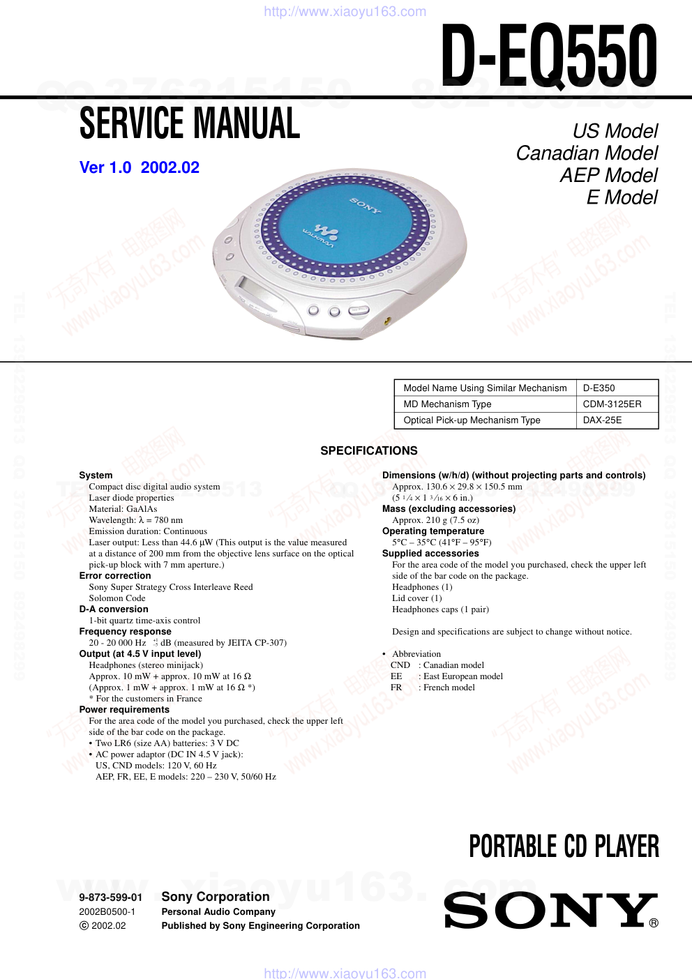
SERVICE MANUAL
PORTABLE CD PLAYER
D-EQ550
Ver 1.0 2002.02
US Model
Canadian Model
AEP Model
E Model
Model Name Using Similar Mechanism
D-E350
MD Mechanism Type
CDM-3125ER
Optical Pick-up Mechanism Type
DAX-25E
9-873-599-01
Sony Corporation
2002B0500-1
Personal Audio Company
C 2002.02
Published by Sony Engineering Corporation
SPECIFICATIONS
System
Compact disc digital audio system
Laser diode properties
Material: GaAlAs
Wavelength: λ = 780 nm
Emission duration: Continuous
Laser output: Less than 44.6 µW (This output is the value measured
at a distance of 200 mm from the objective lens surface on the optical
pick-up block with 7 mm aperture.)
Error correction
Sony Super Strategy Cross Interleave Reed
Solomon Code
D-A conversion
1-bit quartz time-axis control
Frequency response
20 - 20 000 Hz dB (measured by JEITA CP-307)
Output (at 4.5 V input level)
Headphones (stereo minijack)
Approx. 10 mW + approx. 10 mW at 16 Ω
(Approx. 1 mW + approx. 1 mW at 16 Ω *)
* For the customers in France
Power requirements
For the area code of the model you purchased, check the upper left
side of the bar code on the package.
• Two LR6 (size AA) batteries: 3 V DC
• AC power adaptor (DC IN 4.5 V jack):
US, CND models: 120 V, 60 Hz
AEP, FR, EE, E models: 220 – 230 V, 50/60 Hz
Dimensions (w/h/d) (without projecting parts and controls)
Approx. 130.6 × 29.8 × 150.5 mm
(5 1 ⁄4 × 1 3 ⁄16 × 6 in.)
Mass (excluding accessories)
Approx. 210 g (7.5 oz)
Operating temperature
5°C – 35°C (41°F – 95°F)
Supplied accessories
For the area code of the model you purchased, check the upper left
side of the bar code on the package.
Headphones (1)
Lid cover (1)
Headphones caps (1 pair)
Design and specifications are subject to change without notice.
• Abbreviation
CND
: Canadian model
EE
: East European model
FR
: French model
+1
–5
www. xiaoyu163. com
QQ 376315150
9
9
2
8
9
4
2
9
8
TEL 13942296513
9
9
2
8
9
4
2
9
8
0
5
1
5
1
3
6
7
3
Q
Q
TEL 13942296513 QQ 376315150 892498299
TEL 13942296513 QQ 376315150 892498299
http://www.xiaoyu163.com
2
D-EQ550
On the AC power adaptor
• Use only the supplied AC power adaptor. If your player is not
supplied with it, use AC-E45HG AC power adaptor. Do not use
any other AC power adaptor.
DANGER
Invisible laser radiation when open and interlock failed or defeated.
Avoid direct exposure to beam.
1.
SERVICING NOTES ................................................
3
2.
GENERAL
Locating the Controls......................................................
3
3.
DISASSEMBLY
3-1.
Disassembly Flow ...........................................................
4
3-2.
Cabinet (Lower), MD ASSY ..........................................
4
3-3.
Main Board......................................................................
5
3-4.
Turn Table Motor ASSY (Spindle) (M901) ...................
5
3-5.
Optical Pick-up (DAX-25E) ...........................................
6
4.
ELECTRICAL ADJUSTMENTS ..........................
7
5.
DIAGRAMS
5-1.
Block Diagram ................................................................
8
5-2.
Note for Printed Wiring Board and
Schematic Diagrams .......................................................
9
5-3.
Printed Wiring Board ...................................................... 10
5-4.
Schematic Diagram – MAIN Section (1/3) – ................ 11
5-5.
Schematic Diagram – MAIN Section (2/3) – ................ 12
5-6.
Schematic Diagram – MAIN Section (3/3) – ................ 13
5-7.
IC Pin Function Description ........................................... 14
6.
EXPLODED VIEWS
6-1.
Cabinet Section ............................................................... 16
6-2.
Optical Pick-up Section (CDM-3125ER)....................... 17
7.
ELECTRICAL PARTS LIST .................................. 18
ATTENTION AU COMPOSANT AYANT RAPPORT
À LA SÉCURITÉ!
LES COMPOSANTS IDENTIFIÉS PAR UNE MARQUE 0 SUR LES
DIAGRAMMES SCHÉMATIQUES ET LA LISTE DES PIÈCES
SONT CRITIQUES POUR LA SÉCURITÉ DE FONCTIONNEMENT.
NE REMPLACER CES COMPOSANTS QUE PAR DES PIÈCES
SONY DONT LES NUMÉROS SONT DONNÉS DANS CE MANUEL
OU DANS LES SUPPLÉMENTS PUBLIÉS PAR SONY.
SAFETY-RELATED COMPONENT WARNING!!
COMPONENTS IDENTIFIED BY MARK 0 OR DOTTED LINE
WITH MARK 0 ON THE SCHEMATIC DIAGRAMS AND IN THE
PARTS LIST ARE CRITICAL TO SAFE OPERATION.
REPLACE THESE COMPONENTS WITH SONY PARTS WHOSE
PART NUMBERS APPEAR AS SHOWN IN THIS MANUAL OR IN
SUPPLEMENTS PUBLISHED BY SONY.
Flexible Circuit Board Repairing
• Keep the temperature of the soldering iron around 270°C during
repairing.
• Do not touch the soldering iron on the same conductor of the
circuit board (within 3 times).
• Be careful not to apply force on the conductor when soldering or
unsoldering.
Notes on chip component replacement
• Never reuse a disconnected chip component.
• Notice that the minus side of a tantalum capacitor may be dam-
aged by heat.
TABLE OF CONTENTS
This Compact Disc player is
classified as a CLASS 1 LASER
product.
The CLASS 1 LASER
PRODUCT label is located on
the rear exterior.
Laser component in this product is capable of emitting
radiation exceeding the limit for Class 1.
Polarity of the plug
CAUTION
Use of controls or adjustments or performance of procedures other
than those specified herein may result in hazardous radiation
exposure.
www. xiaoyu163. com
QQ 376315150
9
9
2
8
9
4
2
9
8
TEL 13942296513
9
9
2
8
9
4
2
9
8
0
5
1
5
1
3
6
7
3
Q
Q
TEL 13942296513 QQ 376315150 892498299
TEL 13942296513 QQ 376315150 892498299
http://www.xiaoyu163.com
3
D-EQ550
The laser diode in the optical pick-up block may suffer electrostatic
breakdown because of the potential difference generated by the charged
electrostatic load, etc. on clothing and the human body. During repair,
pay attention to electrostatic breakdown and also use the procedure in
the printed matter which is included in the repair parts.
The flexible board is easily damaged and should be handled with care.
NOTES ON LASER DIODE EMISSION CHECK
The laser beam on this model is concentrated so as to be focused on the
disc reflective surface by the objective lens in the optical pick-up block.
Therefore, when checking the laser diode emission, observe from more
than 30cm away from the objective lens.
Before Replacing the Optical pick-up Block
Please be sure to check thoroughly the parameters as per the “Optical
pick-up Block Checking Procedure” (Part No. : 9-960-027-11) issued
separately before replacing the optical Pick-up block.
Note and specifications required to check are given below.
• FOK output : IC601 yg pin
When checking FOK, remove the lead wire to disc motor.
• RF signal P-to-P value : 0.45 to 0.65Vp-p
Combination of Cover Plate Accessories
Set
Accessories
ORANGE (DOT)
BLUE (BUTTERFLY)
BLUE (JEWELRY)
PINK (HEART)
SECTION 1
SERVICING NOTES
Laser Diode Checking Methods
During normal operation of the equipment, emission of the laser diode
is prohibited unless the upper panel is closed while turning ON the S801
(push switch type).
The following two checking methods for the laser diode are operable.
Method :
Emission of the laser diode is visually checked.
1. Open the upper lid.
2. Push the S801 as shown in Fig. 1 .
3. Check the object lens for confirming normal emission of the laser
diode. If not emitting, there is a trouble in the automatic power
control circuit or the optical pick-up. During normal operation, the
laser diode is turned ON about 2.5 seconds for focus searching.
NOTES ON HANDLING THE OPTICAL PICK-UP BLOCK OR
BASE UNIT
Fig.1 Method to push S801
S801
SECTION 2
GENERAL
LOCATING THE CONTROLS
HOLD .
i
VOL–
VOL+ SOUND
ESP
OPEN
DISPLAY
DC IN 4.5V
.
x
>B
MENU
www. xiaoyu163. com
QQ 376315150
9
9
2
8
9
4
2
9
8
TEL 13942296513
9
9
2
8
9
4
2
9
8
0
5
1
5
1
3
6
7
3
Q
Q
TEL 13942296513 QQ 376315150 892498299
TEL 13942296513 QQ 376315150 892498299
http://www.xiaoyu163.com
4
D-EQ550
SECTION 3
DISASSEMBLY
SET
3-2. CABINET (LOWER),
MD ASSY
(Page 4)
3-4. TURN TABLE MOTOR
ASSY (SPINDLE) (M901)
(Page 5)
3-5. OPTICAL PICK-UP
(DAX-25E)
(Page 6)
3-3. MAIN BOARD
(Page 5)
• This set can be disassembled in the order shown below.
3-1.
DISASSEMBLY FLOW
Note: Follow the disassembly procedure in the numerical order given.
3-2.
CABINET (LOWER), MD ASSY
5 Claw
cabinet (lower)
cabinet (front)
MD assy
6
q;
lid upper
1
5 two claws
5 claws
7 flexible board (CN501)
8 connector (CN503) (white)
9 connector (CN502) (black)
5 two claws
3 Open the battery lid.
4 two screws (B2 x 10)
2 three screws (B2 x 10)
www. xiaoyu163. com
QQ 376315150
9
9
2
8
9
4
2
9
8
TEL 13942296513
9
9
2
8
9
4
2
9
8
0
5
1
5
1
3
6
7
3
Q
Q
TEL 13942296513 QQ 376315150 892498299
TEL 13942296513 QQ 376315150 892498299
http://www.xiaoyu163.com
5
D-EQ550
3-3.
MAIN BOARD
3-4.
TURN TABLE MOTOR ASSY
(SPINDLE) (M901)
main board
cabinet (lower)
1
2
turn table motor assy
(spindle) (M901)
1 three screws
(B1.7 × 5)
Chassis
www. xiaoyu163. com
QQ 376315150
9
9
2
8
9
4
2
9
8
TEL 13942296513
9
9
2
8
9
4
2
9
8
0
5
1
5
1
3
6
7
3
Q
Q
TEL 13942296513 QQ 376315150 892498299
TEL 13942296513 QQ 376315150 892498299
http://www.xiaoyu163.com
6
D-EQ550
3-5.
OPTICAL PICK-UP (DAX-25E)
3
5
6
2
1 screw (B 1.7 × 5)
4 screw
(P 1.4 × 3.5)
feed screw assy
chassis
optical pick-up
(DAX-25E)
bracket (Shaft)
gear B
gear cover
motor assy (sled) (M902)
www. xiaoyu163. com
QQ 376315150
9
9
2
8
9
4
2
9
8
TEL 13942296513
9
9
2
8
9
4
2
9
8
0
5
1
5
1
3
6
7
3
Q
Q
TEL 13942296513 QQ 376315150 892498299
TEL 13942296513 QQ 376315150 892498299
http://www.xiaoyu163.com
D-EQ550
7
7
Focus bias Check
Condition:
• Hold the set in horizontal state.
Connection:
Procedure:
1. Connect the oscilloscope to the test points TJ503(RFI) and TJ610
(VBIAS) on the MAIN board.
2. Set a disc. (YEDS-18)
3. Press the >B button.
4. Check the oscilloscope waveform is as shown below.
A good eye pattern means that the diamond shape (◊) in the
center of the waveform can be clearly distinguished.
RF Signal reference Waveform (Eye Pattern)
To watch the eye pattern, set the oscilloscope to AC range and
increase the vertical sensitivity of the oscilloscope for easy
watching.
5. Stop revolving of the disc motor by pressing the x button.
S801
(OPEN/CLOS
C301
C619
C802
IC603
TP814
C106
R620
TAP806
C634
TJ502
R631
TJ608
TP817
TP609
TP616
R824
0
TP503
TJ303
C306
R209
C10
TJ603
C203
TP507
TJ610
R205
TP603
TJ604
D801
TAP803
TJ405
TJ601
TJ602
TJ607
TAP805
TJ501
Q601
TJ503
TAP601
TP621
IC302
R109
C206
C610
R605
R107
D805
R617
R613
R614
R615
L601
HPLOUT
AVDD
AGND
LD
RFI
AVDD
LASER
MON1
MON2
CLK4M
FOK
RF1
SCOR
XBUSY
C2POEN
PD
VBIAS
OPSTB
RFGO
.4V
TJ610 (VBIAS)
TJ503(RFI)
oscilloscope
(AC range)
The CD section adjustments are done automatically in this set.
Precautions for Check
1. Perform check in the order given.
2. Use YEDS-18 disc (Part No.: 3-702-101-01) unless otherwise
indicated.
3. Power supply voltage requirement : DC4.5 V in DC IN jack.
(J401)
VOLUME button : Minimum
HOLD switch : OFF
– MAIN BOARD (SIDE B) –
RF level
0.45 to 0.70 Vp-p
VOLT/DIV : 100 mV (With the 10 : 1 probe in use)
TIME/DIV : 500ns
SECTION 4
ELECTRICAL ADJUSTMENTS
w w w
.
x i a o y u 1 6 3 .
c o m
Q Q
3 7 6 3 1 5 1 5 0
9
9
2
8
9
4
2
9
8
T E L
1 3 9 4 2 2 9 6 5 1 3
9
9
2
8
9
4
2
9
8
0
5
1
5
1
3
6
7
3
Q
Q
TEL 13942296513 QQ 376315150 892498299
TEL 13942296513 QQ 376315150 892498299
http://www.xiaoyu163.com
D-EQ550
8
8
Q401
88,87,85,84
4
1,2,24,25
5,9-12,14-18
23 3
90 83 89
22
52
51
CH3
H
BRIDGE
CH2
H
BRIDGE
CH1
H
BRIDGE
LEVEL
SHIFTER
49
50
33
35
24
46
27
55
E
OPTICAL
PICK-UP
BLOCK
(DAX-25E)
F
OPGSW
LD
PD
F+
F-
T+
T-
S+
S-
C+
C-
OPSTB
A
RF
OP IC
A
RF
FO1
RO2
FO2
RO3
FO3
RO1
FO4
RO4
36 VM12
40 VM2
41 VM3
26 VM34
FOCUS
COIL
TRACKING
COIL
M
M902
SLED
MOTOR
M901
SPINDLE
MOTOR M
F3
FIN+
FIN-
CPOL
CDUTY
R3
FR4
PWM4
31
32
LEVEL
SHIFTER
I/F
29
F2
TIN+
TIN-
SIN+
SIN-
FIN+
FIN-
CPOL
CDUTY
TIN+
TIN-
SIN+
SIN-
R2
FI
30
RI
28
27
26
25
LATCH
DATA
CLOCK
WAKEUP
FI1
23
RESET
XRST_O
SCOR_I
POFF_O
XBUSY_I
DEFECT_I
FOK_I
ESPLT_O
AD_BATMNT
BEEP_O
AMUTE_O
XIN_I
IC603 RAM(4M)
D0-3
A0-10
D0-D3
88,87,85,84
AO-A10
AD_CHG MNT
WP/AD,DSINMNT
BATN2
IC801
SYSTEM
CONTROL
MICON
XRAS
XCAS
XWE
XRAS
XCAS
XWE
42 - 55
57 - 60
28
SEG1
I
SEG14
COM0
I
COM3
LIQUID
CRYSTAL
DISPLAY
LCD801
WP/XOPEN
40
HOLD_I
38
CMPON_I
5
VCPU
25
WP/AD_KEY_1
23
AD-KEY_2
11
7
77
13
72
24
44
16
14
1
5
6
SCGFS_I
71
76
75 74 72 73 77 76 79 78
38
37
40
44
43 45 52 64 65 68 70
5
71
74
30
2
13
14
15
7
20
19
17
31
29
8
6
4
9
8
6
7
2
15 R/XW_O
X POWLT_O
14
(SENS)MSDTI_I
16
MSDTO.O
17
SCK_O
18
XWAKEUP_O
66
XRESET_I
VBATT
49
OPG_O
79
XOPSTBY_O
78
HPSW_O
12
47 48 49 50
RF
AMP
APC
SERVO CORE
PWM
CLOCK
OSC
SIO
WINDOW
ECC
ESP
OUT
IN
IC403
+2V REG.
3
15
10
6
13
54
2
62
1
5 OUT
IN
IC402
+2V REG.
5
2 OUT
IN
IC405
RESET
5
4 OUT
IN
1
CTRL
IC404
+5V REG.
DC IN 4.5V
J401
L401
REGB
DC IN
D404
Q403
D402
D801
VBATT
SWITCGING
REG.
SWITCGING
REG.
4
DRY BATTERY
SIZE" AA"
(IEC DESIGNATION LR6)
2PCS,3V
0R
RECHARGEABLE BATTERY
NC-WMAA/NH-WM2AA
2.4V
S801
DOOR
OPEN
ON OFF
S807
S806
S811
MENU
S809
VOL+
SOUND
VOL-
S808
S808
S810
S803
ESP
ON OFF
DEFFERNTIAL
Q402
44
37
39
RF
A
B
E
F
LD
PD
3
VBATT
IC401(1/2)
FOCUS/TRACKING COIL DRIVE
SLED/SPINDLE MOTOR DRIVE
IC601
RF AMP,DIGITAL SERVO
DIGITAL SIGNAL PROCESSOR
IC302
HEADPHONE AMP
IC401(2/2)
SWITCHING REGURATOR
48
42
CH4
H
BRIDGE
DAC
LOUT
LIN
RIN
BEEP
MUTE
PWRSW
LDACO
RDACO
ROUT
VREF
VBATT
LD
DRIVER
Q601
FDOP
FDON
CLVON
CLVOP
TDOP
TDON
SDOP
SDON
CLKDRV
XOUT
XIN
XRST
SBSY
XPWMN
XBUSY
FOK
DEFECT
YMLD
GFS
VCHK
X4M/8M
CLK4M
SCOK
SRW
SDIN
SDOUT
VBATT
AVDD+2V
VCC+2.2V
VCPU+2V
+3V
VCC1-OUT
VCC1-IN
STNG
VMMNT
VCPU
CHGMNT
Q405
GATE
VCPU+2V
AVDD+2V
VCC0
VIN
: CD PLAY
J301
X171
90MHz
53
S802
HOLD
SIGNAL PATH
SECTION 5
DIAGRAMS
5-1.
BLOCK DIAGRAM
w w w
.
x i a o y u 1 6 3 .
c o m
Q Q
3 7 6 3 1 5 1 5 0
9
9
2
8
9
4
2
9
8
T E L
1 3 9 4 2 2 9 6 5 1 3
9
9
2
8
9
4
2
9
8
0
5
1
5
1
3
6
7
3
Q
Q
TEL 13942296513 QQ 376315150 892498299
TEL 13942296513 QQ 376315150 892498299
http://www.xiaoyu163.com
D-EQ550
9
9
5
4
1
3
2
5-2.
NOTE FOR PRINTED WIRING BOARD AND SCHEMATIC DIAGRAMS
Note on Printed Wiring Board:
• X : parts extracted from the component side.
• Y : parts extracted from the conductor side.
•
: Pattern from the side which enables seeing.
(The other layers' patterns are not indicated.)
Caution:
Pattern face side:
Parts on the pattern face side seen from
(Conductor Side)
the pattern face are indicated.
Parts face side:
Parts on the parts face side seen from
(Component Side)
the parts face are indicated.
Note on Schematic Diagrams:
• All capacitors are in µF unless otherwise noted. pF: µµF
50 WV or less are not indicated except for electrolytics
and tantalums.
• All resistors are in Ω and 1/4 W or less unless otherwise
specified.
•
f
: internal component.
Note:
The components identi-
fied by mark 0 or dotted
line with mark 0 are criti-
cal for safety.
Replace only with part
number specified.
Note:
Les composants identifiés par
une marque 0 sont critiques
pour la sécurité.
Ne les remplacer que par une
pièce portant le numéro
spécifié.
• A : B+ Line.
• Power voltage is dc 3 V and fed with regulated dc power
supply from external power voltage jack.
• Voltages are dc with respect to ground under no-signal
conditions.
• Voltages are taken with a VOM (Input impedance 10 MΩ).
Voltage variations may be noted due to normal produc-
tion tolerances.
• Waveforms are taken with a oscilloscope.
Voltage variations may be noted due to normal produc-
tion tolerances.
• Circled numbers refer to waveforms.
• Signal path.
E
: CD PLAY
• Abbreviation
FR
: French model
• Waveforms
IC601
ek X OUT
VOLT/DIV : 1 V AC
TIME/DIV : 50 nsec
IC801
2 XIN_I
IC401
4 LG
VOLT/DIV : 1 V AC
TIME/DIV : 200 nsec
PLAY MODE
VOLT/DIV : 2 V AC
TIME/DIV : 2 µsec
VOLT/DIV : 1 V AC
TIME/DIV : 2 µsec
2 p-p
16.9 MHz
2.6 p-p
4.24 MHz
6.2 Vp-p
5.6 µsec
3 Vp-p
5.6 µsec
IC401
9 USW
IC601
qh RFGO
VOLT/DIV : 0.1 V AC
TIME/DIV : 0.5 msec
0.45-0.65 Vp-p
• Abbreviation
FR
: French model
w w w
.
x i a o y u 1 6 3 .
c o m
Q Q
3 7 6 3 1 5 1 5 0
9
9
2
8
9
4
2
9
8
T E L
1 3 9 4 2 2 9 6 5 1 3
9
9
2
8
9
4
2
9
8
0
5
1
5
1
3
6
7
3
Q
Q
TEL 13942296513 QQ 376315150 892498299
TEL 13942296513 QQ 376315150 892498299
http://www.xiaoyu163.com
D-EQ550
10
10
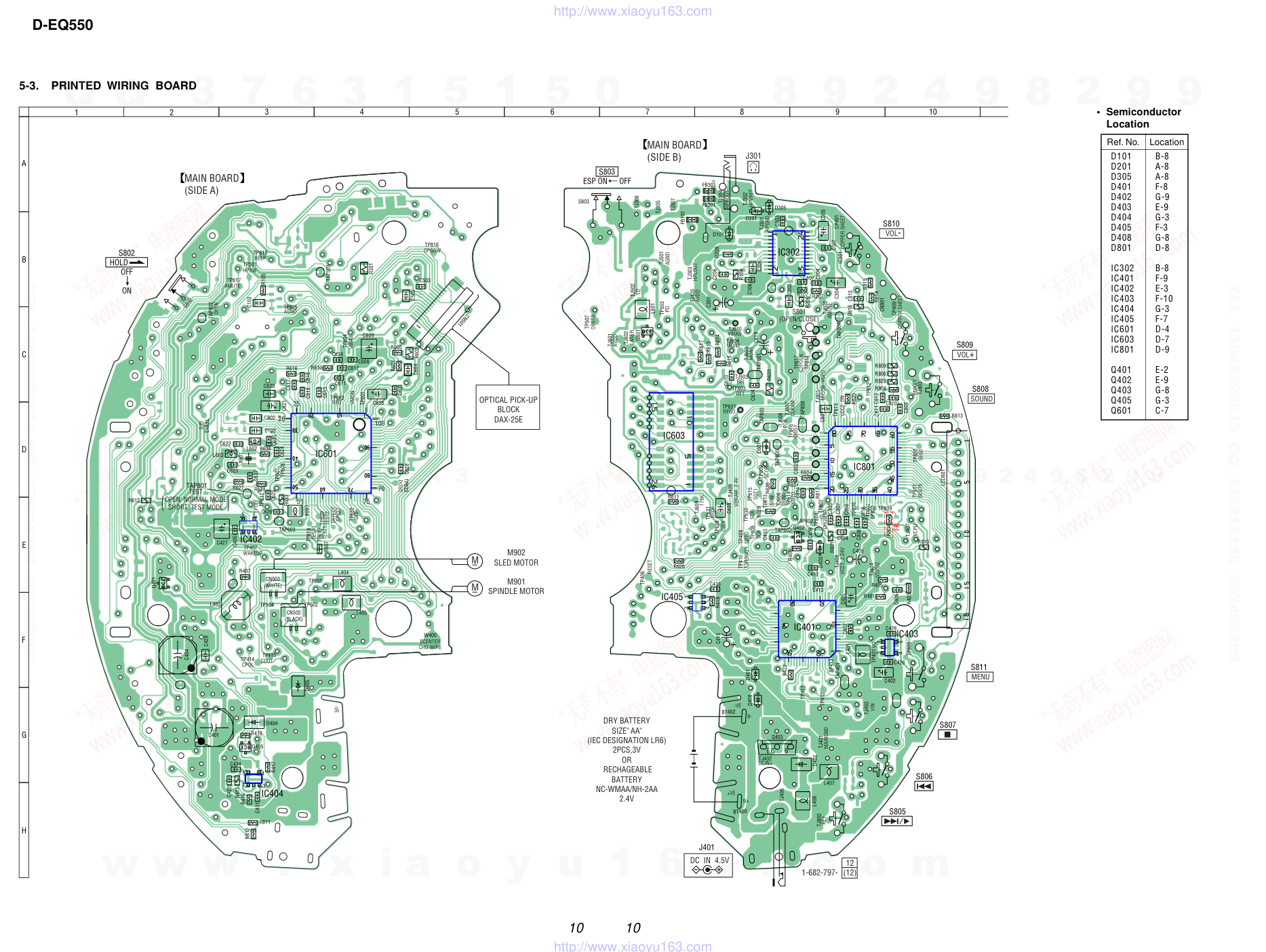
5-3.
PRINTED WIRING BOARD
MAIN BOARD
(SIDE B)
MAIN BOARD
(SIDE A)
12
(12)
1-682-797-
M902
SLED MOTOR
M901
SPINDLE MOTOR
M
M
OPTICAL PICK-UP
BLOCK
DAX-25E
S802
HOLD
OFF
ON
DC IN 4.5V
S801
(OPEN/CLOSE)
C301
C619
S810
S809
S808
S811
LCD801
C408
C415
BT400
BT402
B+
B-
+VE
-VE
Q403
S806
S807
S805
DRY BATTERY
SIZE" AA"
(IEC DESIGNATION LR6)
2PCS,3V
OR
RECHAGEABLE
BATTERY
NC-WMAA/NH-2AA
2.4V
2
3
4
5
6
7
8
9
10
A
1
B
C
D
E
F
G
H
25
26
51
75
76
100
E
B
C
J301
C802
IC603
TP814
IC401
IC801
TP413
C106
C402
TP412
R620
D408
TP411
TJ402
TAP401
TJ403
C425
TJ801
TP401
D402
TP612
TAP806
C810
TJ609
R626
R814
TJ406
IC403
R403
R804
C407
C406
TJ401
R405
TJ404
C634
C629
TJ502
IC405
IC301
C412
C409
C814
Q402
C410
TP812
R207
R816
TAP402
C304
C813
R406
TAP602
TP807
R801
C806
R631
C812
TAP804
C811
R815
C307
R809
TJ608
CN901
C801
TP817
R808
TP609
TP410
TP616
R824
R630
TP613
TP802
TP803
TP503
C809
TJ409
TJ304
TJ303
FB301
FB101
TJ605
C306
R209
C107
TJ307
TJ603
C428
TP809
TP409
TP806
TJ803
TP811
TP804
TP406
TP628
R629
R611
TJ802
TP615
TP820
TP631
D401
C433
C203
TP408
TP507
TJ610
R205
TP603
TJ604
D801
TAP803
TJ405
TJ407
TJ601
TJ602
TJ606
TJ607
TAP805
FB201
TP614
TJ501
Q601
C303
TJ408
TJ503
TP815
TAP601
TJ302
TJ306
TJ301
TP621
R820
C818
R810
IC302
R109
C206
C204
C610
R419
3
1
4
6
3
1
4
5
C426
R401
TP805
R422
R107
C305
CP400
J401
TJ305
C804
C805
C807
C808
R617
R613
R614
R615
R823
R806
CP401
L407
L601
L406
L401
R817
HPGND
HPVREF
HPLOUT
HPROUT
MAINGND
DCIN+
VIN
VCPU2
AVDD
VCPU
AGND
LD
RFI
AVDD
LASER
MON1
MON2
AMUTE
DGND
CLK4M
FOK
176K
KEY
RMKEY
VG
RESET
SCK
SDTO
POWERLT
RF1
SCOR
SCK
SRW
SDTO
SDT1
XBUSY
C2FX
XROF
CHGMNT
SEG15
SEG0
VCC2_ON
C2POEN
PD
VBIAS
MICON_VCPU
OPSTB
RFGO
COPPER SHEET
VCC1_2.24V
VDRAM_2.4V
COPPER SHEET
S802
TP819
TP301
TAP301
R105
C502
TAP802
TP816
HPSW
OPGSW
BEEP
C608
TP602
C617
C503
R301
CN501
R616
C616
R610
C618
C613
R601
C612
TP601
C604
R602
R603
C609
TP605
TP617
TP604
OPEN
VMON
RFO
VBIAS
AGND
AMUTE
C638
TP813
C103
C621
C603
C611
C614
C620
C202
GFS
C102
TP501
R633
TP627
TP504
C625
R636
L604
TP620
R628
C637
TP611
TP632
R612
L405
L404
CN502
(BLACK)
CN503
(WHITE)
T-
TEST2
DEFECT
GFS
R407
TP407
TP502
TP414
TP415
WAKEUP
F-
CPOL
CDUT
C623
Q401
R627
R607
C427
C628
IC601
TAP603
TP618
C635
TP633
TP619
L602
C622
C626
TP607
C624
L603
TAP801
TP608
TEST
OPEN: NORMAL MODE
SHORT: TEST MODE
POFF
TEST0
TEST1
DOUT
-VE
C404
C429
X601
IC402
D405
W400
D404
L402
C405
C401
BCENTER
CHG WIRE
R811
R416
C422
R417
1
3
5
4
R415
R410
C434
R812
C431
IC404
Q405
S803
ESP ON OFF
VOL-
VOL+
SOUND
MENU
1
3
5
4
S803
R813
FR
C413
D403
D305
D101
D201
• Semiconductor
Location
D101
D201
D305
D401
D402
D403
D404
D405
D408
D801
IC302
IC401
IC402
IC403
IC404
IC405
IC601
IC603
IC801
Q401
Q402
Q403
Q405
Q601
B-8
A-8
A-8
F-8
G-9
E-9
G-3
F-3
G-8
D-8
B-8
F-9
E-3
F-10
G-3
F-7
D-4
D-7
D-9
E-2
E-9
G-8
G-3
C-7
Ref. No.
Location
w w w
.
x i a o y u 1 6 3 .
c o m
Q Q
3 7 6 3 1 5 1 5 0
9
9
2
8
9
4
2
9
8
T E L
1 3 9 4 2 2 9 6 5 1 3
9
9
2
8
9
4
2
9
8
0
5
1
5
1
3
6
7
3
Q
Q
TEL 13942296513 QQ 376315150 892498299
TEL 13942296513 QQ 376315150 892498299
http://www.xiaoyu163.com
D-EQ550
11
11
5-4.
SCHEMATIC DIAGRAM – MAIN SECTION (1/3) –
• Refer to page 9 for Waveforms.
• Refer to page 15 for IC Block Diagrams.
IC404
Q402
Q405
Q401
IC405
L406
1µH
L407
1µH
D402
D405
R416
R415
C422
R417
D404
C431
C434
R410
C429
L401
220µH
47µH
C402
C426
C401
C407
C425
C408
L402
R401
C404
C406
R403
TAP402
C405
C427
C409
D403
C410
C412
C413
R407
C433
R419
L404
10µH
L405
10µH
D401
C415
R422
C502
CN502
CN503
CN501
C503
TP413
TP412
TP411
TP403
TP404
D408
IC403
C428
R406
IC402
J401
BT400
BT402
MM1385AN
DTC143TUA
2SC4116GL
2SB16790
XC61CN1402MR
MA2YD
MA2YD2300L
47k
220k
0.22
47k
MA2YD2300L
0.01
0.1
1k
2.2
4.7
16V
0.1
100
6.3V
0.1
10
4V
100
4V
100k
100
6.3V
2200p
10k
0.1
10
4V
0.22
MA111-TX
1
0.047
1000p
470k
0.01
0
UDZS5.1B
220
6.3V
0
2.2
2P
2P
15 PIN
0.1
POWER_IC
TEST
UDZS5.1
XC6201P242
0.1
100k
XC6201P212MR
GND
2.2V
VCPU 2V
VDD
3V
SYNC
B3
AVDD 2V
DCINMNT
RF
B1
CPOL
CDUTY
SIN+
SIN-
TIN+
TIN-
FIN-
FIN+
T+
S-
S+
T-
F-
F+
C+
PD
LD
F
E
OPSTB
B
A
OPGSW
C-
BATMNT
CHGMNT
C-
C+
S-
S+
F+
T+
T-
F-
RESET
POWERLT
SDTO
SCK
XWAKEUP
RESET
RESET
XWAKEUP
SYNC
FO1
PGND1
RO1
FO2
PGND2
RO2
FO3
RO3
PGND3
FO4
PGND4
RO4
R3
F3
R2
F2
R1
F1
LATCH
DATA
CLOCK
WAKEUP
RESET
VCPU
VREF
SLOW
STNG
EO
EI
VCC0
USW
DSW
VIN
LG
VG
INM
DCIN
GSW
SEO
SEI
PREGND
BATM1
BATM2
CHGMNT
VCC2
VCC0
VCC1-IN
VCC1-OUT
SOFT
VCPUNF
VMMNT
VG
PREGND2
REGB
DGND
PGND5
CHGB
PMG
VM12
VM2
VM3
VM34
PWM4
FR4
SAWMON
DET
SPINDLE MOTOR
GREEN
WHITE
SLED MOTOR
GND
NC
NC
IN
OUT
GND
NC
NC
IN
OUT
GND
NSE
CTRL
IN
OUT
OUT
GND
NC
VIN
Cd
DC IN 4.5V
OPIC
VCC
M901
M902
COIL
TRACKING
COIL
FOCUS
LD
PD
DEFFERENTIAL
RESET
+2V REG
+5V REG
GATE
SWITCH
DRY BATTERY
SIZE"AA"
(IEC DESIGNATION LR6)
2PCS,3V
OR
BATTERY
RECHARGEABLE
NC-WMAAA/NH-WM2AA
2.4V
+2.4V REG
IC401
BH6571KVT
FOCUS/TRACKING COIL DRIVE
SLED/SPINDLE MOTOR DRIVE
SWITCHING REGULATOR
R405
1M
Q403
SWITCH
2SB1237PQR
The components identified by mark 0 or dotted
line with mark 0 are critical for safety.
Replace only with part number specified.
Les composants identifiés par une marque 0 sont
critiques pour la sécurité.
Ne les remplacer que
par une pièce portant le numéro spécifié.
w w w
.
x i a o y u 1 6 3 .
c o m
Q Q
3 7 6 3 1 5 1 5 0
9
9
2
8
9
4
2
9
8
T E L
1 3 9 4 2 2 9 6 5 1 3
9
9
2
8
9
4
2
9
8
0
5
1
5
1
3
6
7
3
Q
Q
TEL 13942296513 QQ 376315150 892498299
TEL 13942296513 QQ 376315150 892498299
http://www.xiaoyu163.com
D-EQ550
12
12
5-5.
SCHEMATIC DIAGRAM – MAIN SECTION (2/3) –
• Refer to page 9 for Waveforms.
TP633
IC302
IC601
IC603
Q601
L601
R602
R603
C604
R601
C638
C603
TP601
TP602
C610
C611
R617
R613
R614
R615
TJ603
TJ604
R610
C614
C616
C617
C618
R616
C608
C609
C634
TAP601
R620
C619
C620
C202
C203
R205
C204
R207
C102
C103
R105
C621
C635
L602
10µH
C628
L604
10µH
TP608
TP607
TP635
TP629
C624
C637
R636
C622
C623
L603
X601
R631
R630
R629
R627
R628
TP634
C304
C307
C305
R301
C301
R109
R209
C206
C106
C306
FB101
FB301
FB201
D201
D305
D101
C629
R633
TP628
R626
TP630
TP626
TP625
TP624
TP623
TP622
R607
R611
TP610
TP606
C626
C625
R107 C107
C303
R612
C612
C613
TP621
TJ610
DOUT
TA2120FN
HP IC
BU9355KS
MSM51V4400E-70SJ
DRAM(4M)
2SB16790
2.2
100k
2.2
470
10
4V
0.1
VMON
RFO
0.01
1000p
100k
100k
100k
100k
MON1 (B)
MON2 (B)
0
0.1
47p
0.22
0.22
470
0.1
10
4V
2200p
47
220
6.3V
1
10K
2.2
1000p
10K
2.2
2.2
2200p
0.1
1
0.01
1M
10p
10p
16.9MHz
0
0
0
0
0
10
4V
47p
10
4V
4.7
220
6.3V
4.7
4.7
0.1
0.1
2.2
0
0
0
UDZ5.1B
UDZ5.1B
UDZ5.1B
10
4V
2.2k
C2FX
10k
0
0
47p
0.1
1000p
1
0
0.01
2200p
RFGO
VBIAS
B1
SYNC
B3
AVDD 2V
A0
A1
A2
A3
A4
A5
A6
A7
A8
A9
A10
D0
D1
D2
D3
XRAS
XWE
CPOL
CDUTY
FIN-
FIN+
XCAS
TIN-
TIN+
SIN-
SIN+
ESPLT
GFS
DEFECT
FOK
XBUSY
CLK4M
BEEP
HPSW
AMUTE
SDTI
SDTO
SRW
SCK
POFF
XRST
SCOR
A0
A1
A2
A3
A9
D1
XWE
XRAS
D0
A4
A5
A6
A7
A8
D2
D3
XCAS
PD
A
B
E
F
BATMNT
LD
*
*
*
*
D1
D0
VSS
D3
D2
A0
A1
A2
A3
VCC
A4
A5
A6
A7
A8
A9
XCAS
XOE
XRAS
XWE
AVDD1
AVSS1
AVSS2
AVDD2
DVSSIO1
DVDDIO1
DVSSIO2
DVDDIO2
LD
PD
VMON
VCHK
E
F
VBIAS
RFO
B
A
RFI
PKC
BTC
RFGO
DETI
ASYI
ASYO
MON1
MON2
ADPFO
ADPFI
FCO
PCO
RLINO
RLINI
RDACO
VCDACO
LDACO
LLINI
LLINO
MUTE
XIN
XOUT
SBDAT
SFSY
SBSY
SCLK
SRW
SDIN
SDOUT
CLK4M
DEFECT
FOK
C2FX
EFM/YFLG
YMLD
EXPLCK
SYNC
CLKDRV
CLVON
FDON
FDOP
TDON
TDOP
SDON
SDOP
DIT
A10/CAS2B
D2
D3
D0
D1
A9
A8
A7
A6
A5
A4
A3
A2
A1
A0
XRAS
XWE
XCAS
XBUSY
CLVOP
DVSS2
DVDD2
TEST2
TEST1
TEST0
DVDD1
DVSS1
XPDWN
XRST
TZC
RFZC
ONTRK
ONDIR
TGU
ATTSW
GND
BEEP
BIAS
PGND
VCC
LIN
RIN
LOUT
ROUT
VREF
BBSW
PWRSW
MUTE
ALCDET
ALCIN
MIXOUT
RFIN
ADDOUT
BSTNF
BSTOUT
BIAS_IN
OCLSW
X4M/8M
AMP
HEADPHONE
DIGITAL SIGNAL PROCESSOR
RF AMP,DIGITAL SERVO,
LD DRIVER
FR
EXCEPT FR
*R105,205
22k
10k
FR
EXCEPT FR
*R107,207
4.7k
22k
10µH
MUTE_t
2.2V
VDD
3V
GND
RF
J301
w w w
.
x i a o y u 1 6 3 .
c o m
Q Q
3 7 6 3 1 5 1 5 0
9
9
2
8
9
4
2
9
8
T E L
1 3 9 4 2 2 9 6 5 1 3
9
9
2
8
9
4
2
9
8
0
5
1
5
1
3
6
7
3
Q
Q
TEL 13942296513 QQ 376315150 892498299
TEL 13942296513 QQ 376315150 892498299
http://www.xiaoyu163.com
D-EQ550
13
13
5-6.
SCHEMATIC DIAGRAM – MAIN SECTION (3/3) –
• Refer to page 9 for Waveforms.
S808
S809
S810
S811
C809
C810
C811
C812
TP812
TP815
R820
TAP803
R823
R806
D801
C801
C802
R824
R817
TAP801
C818
R801
C804
C807
Q808
C805
R816
C813
TAP802
S801
S802
S803
S807
S806
S805
R811
R812
R809
R810
R813
R814
R815
C814
TP806
TP807
TP803
TP809
TP811
TP820
R804
CN901
0.1
0.1
0.22
0.1
VCC2_ON
10k
100k
100k
MA2ZD1400
1
0.22
0
100k
TEST
4700p
100k
0.01
0.01
0.01
0.01
220k
4700p
OPEN
(DOOR OPEN)
2.2k
4.7k
10k
10k
2.2k
4.7k
10k
0.1
SEG15
SEG0
10k
B1
GND
DCINMNT
VCPU 2V
HOLD
AMUTE
XRST
POFF
COM0
COM1
COM2
COM3
SEG1
SEG2
SEG3
SEG4
SEG5
SEG6
SEG7
SEG8
SEG9
SEG10
SEG11
SEG12
SEG13
RESET
SRW
SCK
FOK
XBUSY
HOLD
G-PRO
OPEN
SCOR
SDTO
POWERLT
SDTI
CLK4M
G-PRO
GFS
OPEN
OPSTB
HPSW
OPGSW
XWAKEUP
C2PO
SEG14
ESPLT
DEFECT
P23
PGM_SEL
PGM_SCK
PGM_SDTI
PGM_SDTO
RESET2
TEST
CLK4M2
BEEP
BATMNT
CHGMNT
PGM_SCK
PGM_SDTI
PGM_SDTO
PGM_SEL
TEST
RESET2
SEG1
SEG2
SEG3
SEG4
SEG5
SEG6
SEG7
SEG8
SEG9
SEG10
SEG11
SEG12
SEG13
SEG14
COM3
COM2
COM1
COM0
SEG14
SEG13
SEG6
SEG5
SEG4
SEG12
SEG11
SEG10
SEG9
SEG8
SEG7
SEG3
SEG2
SEG1
SEG0
COM3
COM2
COM1
COM0
V3
V2
V1
C1
C0
AMUTE_O
VCC2ON_O
XRST_O
HOLD_I
SEG15
XWAKEUP_O
版权声明
1. 本站所有素材,仅限学习交流,仅展示部分内容,如需查看完整内容,请下载原文件。
2. 会员在本站下载的所有素材,只拥有使用权,著作权归原作者所有。
3. 所有素材,未经合法授权,请勿用于商业用途,会员不得以任何形式发布、传播、复制、转售该素材,否则一律封号处理。
4. 如果素材损害你的权益请联系客服QQ:77594475 处理。