CMI奇美55寸FHD液晶屏维修手册
 "CMI奇美55寸FHD液晶屏维修手册-0")
 "CMI奇美55寸FHD液晶屏维修手册-1")
 "CMI奇美55寸FHD液晶屏维修手册-2")
 "CMI奇美55寸FHD液晶屏维修手册-3")
 "CMI奇美55寸FHD液晶屏维修手册-4")
 "CMI奇美55寸FHD液晶屏维修手册-5")
 "CMI奇美55寸FHD液晶屏维修手册-6")
 "CMI奇美55寸FHD液晶屏维修手册-7")
 "CMI奇美55寸FHD液晶屏维修手册-8")
 "CMI奇美55寸FHD液晶屏维修手册-9")
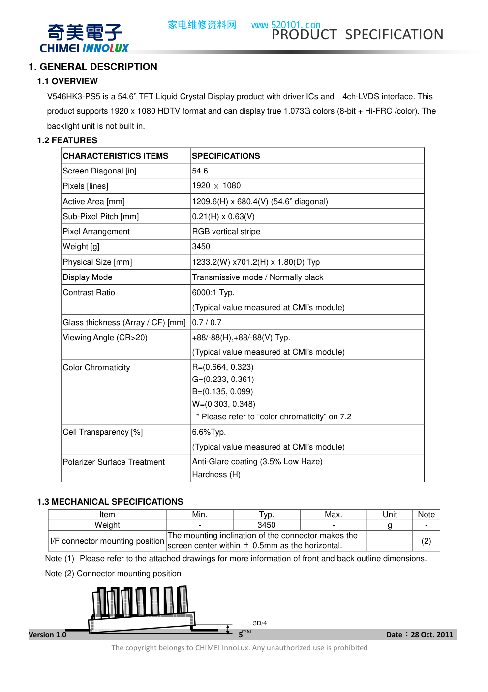
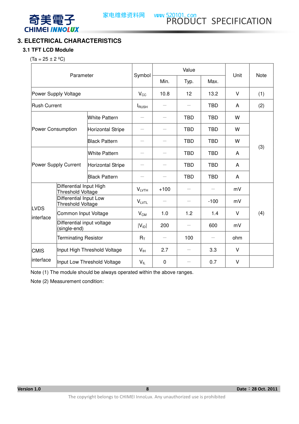
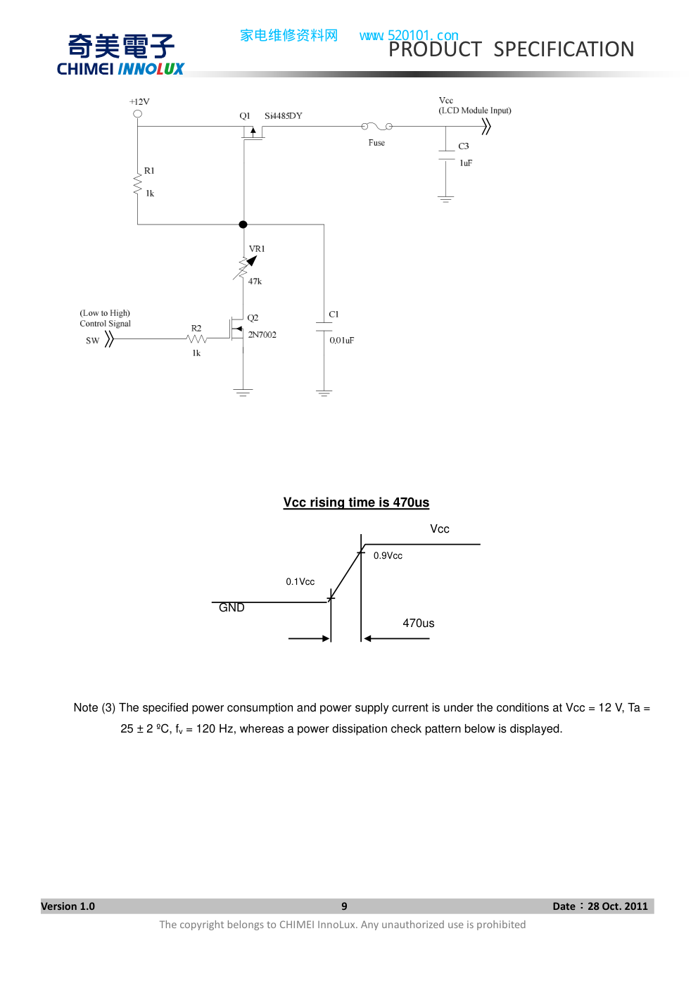
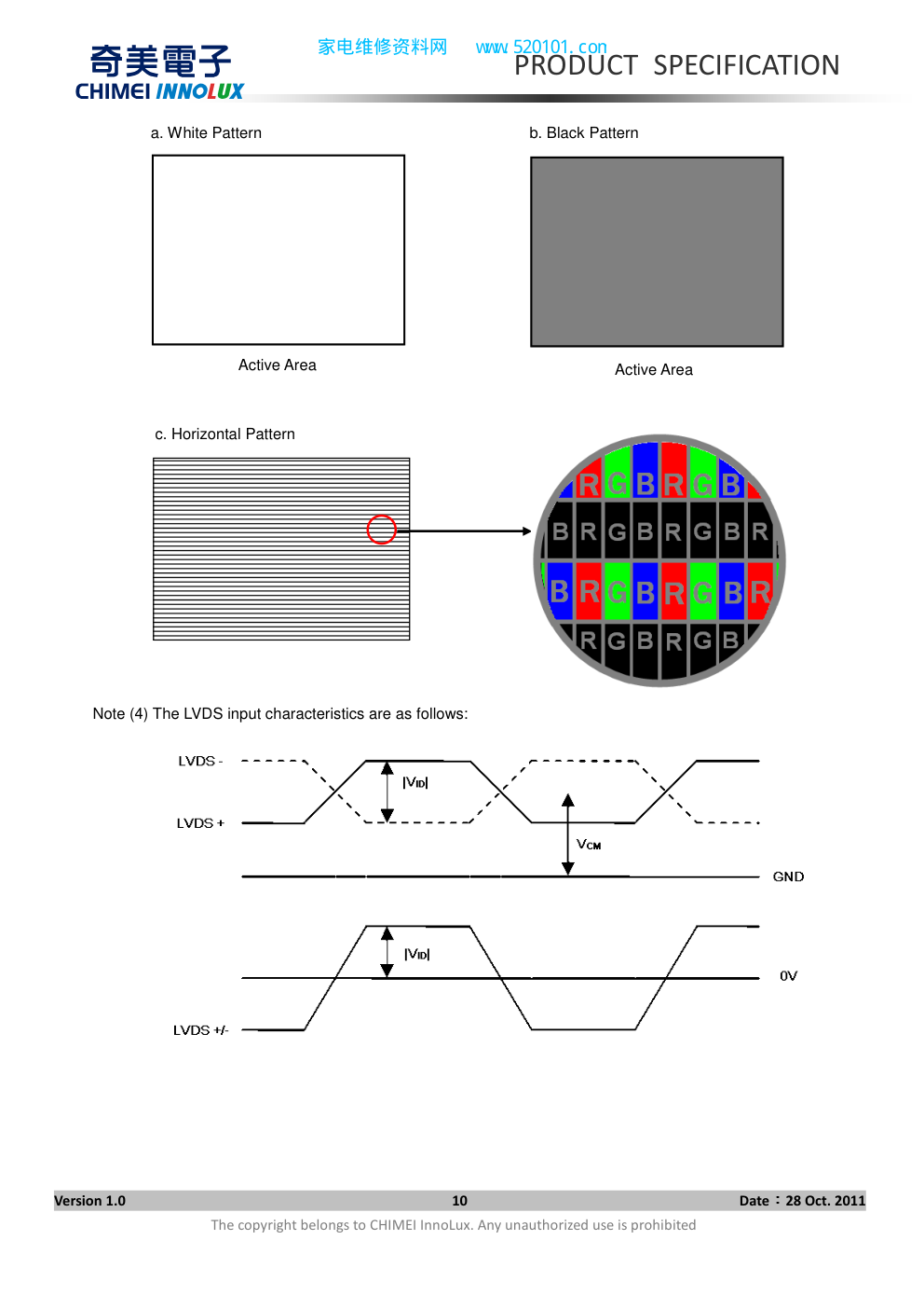
PRODUCT SPECIFICATION Version 1.0 1 Date: : : :28 Oct. 2011 The copyright belongs to CHIMEI InnoLux. Any unauthorized use is prohibited Customer: APPROVED BY SIGNATURE Name / Title Note Please return 1 copy for your confirmation with your signature and comments. □ Tentative Specification ■ Preliminary Specification □ Approval Specification MODEL NO.: V546HK3 SUFFIX: PS5 Approved By Checked By Prepared By Chao-Chun Chung Ken Wu YI-CHEN Chiang 家电维修资料网 www. 520101. com PRODUCT SPECIFICATION Version 1.0 2 Date: : : :28 Oct. 2011 The copyright belongs to CHIMEI InnoLux. Any unauthorized use is prohibited CONTENTS REVISION HISTORY........................................................................................................................................................ 4 1. GENERAL DESCRIPTION........................................................................................................................................... 5 1.1 OVERVIEW ......................................................................................................................................................... 5 1.2 FEATURES.......................................................................................................................................................... 5 1.3 MECHANICAL SPECIFICATIONS...................................................................................................................... 5 2. ABSOLUTE MAXIMUM RATINGS ............................................................................................................................... 6 2.1 ABSOLUTE RATINGS OF ENVIRONMENT....................................................................................................... 6 2.2 ELECTRICAL ABSOLUTE RATINGS(OPEN CELL)........................................................................................... 7 3. ELECTRICAL CHARACTERISTICS ............................................................................................................................ 8 3.1 TFT LCD Module................................................................................................................................................. 8 4. BLOCK DIAGRAM OF INTERFACE ...........................................................................................................................11 4.1 TFT LCD MODULE ............................................................................................................................................11 5 .INPUT TERMINAL PIN ASSIGNMENT ...................................................................................................................... 12 5.1 TFT LCD OPEN CELL ...................................................................................................................................... 12 5.2 LVDS INTERFACE ............................................................................................................................................ 20 5.3 COLOR DATA INPUT ASSIGNMENT ............................................................................................................... 21 6. INTERFACE TIMING.................................................................................................................................................. 24 6.1 INPUT SIGNAL TIMING SPECIFICATIONS ..................................................................................................... 24 6.1.1 Timing spec for Frame Rate = 100Hz ............................................................................................................ 24 6.1.2 Timing spec for Frame Rate = 120Hz ............................................................................................................ 25 6.2 POWER ON/OFF SEQUENCE (Ta = 25 ± 2 ºC)............................................................................................... 28 6.2.1 POWER ON/OFF SEQUENCE...................................................................................................................... 28 6.2.2 2D/3D MODE CHANGE2D to 3D SIGNAL SEQUENCE WITHOUT VCC TURN OFF AND TURN ON ....... 29 7. OPTICAL CHARACTERISTICS ................................................................................................................................. 30 7.1 TEST CONDITIONS.......................................................................................................................................... 30 7.2 OPTICAL SPECIFICATIONS ............................................................................................................................ 31 8.PRECAUTIONS........................................................................................................................................................... 34 8.1 ASSEMBLY AND HANDLING PRECAUTIONS ................................................................................................ 34 家电维修资料网 www. 520101. com PRODUCT SPECIFICATION Version 1.0 3 Date: : : :28 Oct. 2011 The copyright belongs to CHIMEI InnoLux. Any unauthorized use is prohibited 8.2 SAFETY PRECAUTIONS ................................................................................................................................. 34 9. DEFINITION OF LABELS........................................................................................................................................... 35 9.1 OPEN CELL LABEL .......................................................................................................................................... 35 9.2 CARTON LABEL ............................................................................................................................................... 37 10. Packaging................................................................................................................................................................. 38 10.1 PACKING SPECIFICATIONS.......................................................................................................................... 38 10.2 PACKING METHOD........................................................................................................................................ 38 11. MECHANICAL CHARACTERISTIC.......................................................................................................................... 40 Appendix A...................................................................................................................................................................... 42 家电维修资料网 www. 520101. com PRODUCT SPECIFICATION Version 1.0 4 Date: : : :28 Oct. 2011 The copyright belongs to CHIMEI InnoLux. Any unauthorized use is prohibited REVISION HISTORY Version Date Page (New) Section Description A1(0.0) Oct 03,11 all all Tentative Specification Ver 0.0 was first issued. B1(1.0) Oct 28,11 all all Preliminary Specification Ver 1.0 was first issued. 家电维修资料网 www. 520101. com PRODUCT SPECIFICATION Version 1.0 5 Date: : : :28 Oct. 2011 The copyright belongs to CHIMEI InnoLux. Any unauthorized use is prohibited 1. GENERAL DESCRIPTION 1.1 OVERVIEW V546HK3-PS5 is a 54.6” TFT Liquid Crystal Display product with driver ICs and 4ch-LVDS interface. This product supports 1920 x 1080 HDTV format and can display true 1.073G colors (8-bit + Hi-FRC /color). The backlight unit is not built in. 1.2 FEATURES CHARACTERISTICS ITEMS SPECIFICATIONS Screen Diagonal [in] 54.6 Pixels [lines] 1920 × 1080 Active Area [mm] 1209.6(H) x 680.4(V) (54.6” diagonal) Sub-Pixel Pitch [mm] 0.21(H) x 0.63(V) Pixel Arrangement RGB vertical stripe Weight [g] 3450 Physical Size [mm] 1233.2(W) x701.2(H) x 1.80(D) Typ Display Mode Transmissive mode / Normally black Contrast Ratio 6000:1 Typ. (Typical value measured at CMI’s module) Glass thickness (Array / CF) [mm] 0.7 / 0.7 Viewing Angle (CR>20) +88/-88(H),+88/-88(V) Typ. (Typical value measured at CMI’s module) Color Chromaticity R=(0.664, 0.323) G=(0.233, 0.361) B=(0.135, 0.099) W=(0.303, 0.348) * Please refer to “color chromaticity” on 7.2 Cell Transparency [%] 6.6%Typ. (Typical value measured at CMI’s module) Polarizer Surface Treatment Anti-Glare coating (3.5% Low Haze) Hardness (H) 1.3 MECHANICAL SPECIFICATIONS Item Min. Typ. Max. Unit Note Weight - 3450 - g - I/F connector mounting position The mounting inclination of the connector makes the screen center within ± 0.5mm as the horizontal. (2) Note (1) Please refer to the attached drawings for more information of front and back outline dimensions. Note (2) Connector mounting position CN 3D/4 家电维修资料网 www. 520101. com PRODUCT SPECIFICATION Version 1.0 6 Date: : : :28 Oct. 2011 The copyright belongs to CHIMEI InnoLux. Any unauthorized use is prohibited 2. ABSOLUTE MAXIMUM RATINGS 2.1 ABSOLUTE RATINGS OF ENVIRONMENT Value Item Symbol Min. Max. Unit Note Storage Temperature TST -20 +60 ºC (1) With CMI Module Operating Ambient Temperature TOP 0 50 ºC (1), (2) With CMI Module Note (1)Temperature and relative humidity range is shown in the figure below. (a) 90 %RH Max. (Ta ≦ 40 ºC). (b) Wet-bulb temperature should be 39 ºC Max. (Ta > 40 ºC). (c) No condensation. Note (2) The maximum operating temperature is based on the test condition that the surface temperature of display area is less than or equal to 65 ºC with LCD module alone in a temperature controlled chamber. Thermal management should be considered in final product design to prevent the surface temperature of display area from being over 65 ºC. The range of operating temperature may degrade in case of improper thermal management in final product design. Relative Humidity (%RH) Operating Range Temperature (ºC) 100 80 60 -20 40 0 20 -40 90 80 40 60 20 10 Storage Range 家电维修资料网 www. 520101. com PRODUCT SPECIFICATION Version 1.0 7 Date: : : :28 Oct. 2011 The copyright belongs to CHIMEI InnoLux. Any unauthorized use is prohibited 2.2 ELECTRICAL ABSOLUTE RATINGS(OPEN CELL) Storage Condition: With shipping package. Storage temperature range: 25±5 ℃ Storage humidity range: 50±10%RH Shelf life: a month 家电维修资料网 www. 520101. com PRODUCT SPECIFICATION Version 1.0 8 Date: : : :28 Oct. 2011 The copyright belongs to CHIMEI InnoLux. Any unauthorized use is prohibited 3. ELECTRICAL CHARACTERISTICS 3.1 TFT LCD Module (Ta = 25 ± 2 ºC) Value Parameter Symbol Min. Typ. Max. Unit Note Power Supply Voltage VCC 10.8 12 13.2 V (1) Rush Current IRUSH - - TBD A (2) White Pattern - - TBD TBD W Horizontal Stripe - - TBD TBD W Power Consumption Black Pattern - - TBD TBD W White Pattern - - TBD TBD A Horizontal Stripe - - TBD TBD A Power Supply Current Black Pattern - - TBD TBD A (3) Differential Input High Threshold Voltage VLVTH +100 - - mV Differential Input Low Threshold Voltage VLVTL - - -100 mV Common Input Voltage VCM 1.0 1.2 1.4 V Differential input voltage (single-end) |VID| 200 - 600 mV LVDS interface Terminating Resistor RT - 100 - ohm (4) Input High Threshold Voltage VIH 2.7 - 3.3 V CMIS interface Input Low Threshold Voltage VIL 0 - 0.7 V Note (1) The module should be always operated within the above ranges. Note (2) Measurement condition: 家电维修资料网 www. 520101. com PRODUCT SPECIFICATION Version 1.0 9 Date: : : :28 Oct. 2011 The copyright belongs to CHIMEI InnoLux. Any unauthorized use is prohibited Vcc rising time is 470us 470us Vcc GND 0.9Vcc 0.1Vcc Note (3) The specified power consumption and power supply current is under the conditions at Vcc = 12 V, Ta = 25 ± 2 ºC, fv = 120 Hz, whereas a power dissipation check pattern below is displayed. 家电维修资料网 www. 520101. com PRODUCT SPECIFICATION Version 1.0 10 Date: : : :28 Oct. 2011 The copyright belongs to CHIMEI InnoLux. Any unauthorized use is prohibited c. Horizontal Pattern Note (4) The LVDS input characteristics are as follows: Active Area Active Area a. White Pattern b. Black Pattern 家电维修资料网 www. 520101. com PRODUCT SPECIFICATION Version 1.0 11 Date: : : :28 Oct. 2011 The copyright belongs to CHIMEI InnoLux. Any unauthorized use is prohibited 4. BLOCK DIAGRAM OF INTERFACE 4.1 TFT LCD MODULE INPUT CONNECTOR CNF1: FI-RE51S-HF,JAE, or equivalent TFT LCD PANEL (1920x3x1080) DATA DRIVER SCAN DRIVER DC/DC CONVERTER & REFERENCE VOLTAGE INPUT CONNECTOR CNF2: FI-RE41S-HF,JAE, or equivalent GND VCC CH3_0(+/-) CH3_1(+/-) CH3_2(+/-) CH3_3(+/-) CH3_4(+/-) CH3_CLK(+/-) CH4_0(+/-) CH4_1(+/-) CH4_2(+/-) CH4_3(+/-) CH4_4(+/-) CH4_CLK(+/-) TIMING CONTROLLER SELLVDS CH1_0(+/-) CH1_1(+/-) CH1_2(+/-) CH1_3(+/-) CH1_4(+/-) CH1_CLK(+/-) CH2_0(+/-) CH2_1(+/-) CH2_2(+/-) CH2_3(+/-) CH2_4(+/-) CH2_CLK(+/-) 2D/3D L/R LD_EN OUTPUT CONNECTOR CN6:LM123S-010-H-TF1-3 or equivalent L/R_O L/R_O SCN_EN SCL SDA 家电维修资料网 www. 520101. com PRODUCT SPECIFICATION Version 1.0 12 Date: : : :28 Oct. 2011 The copyright belongs to CHIMEI InnoLux. Any unauthorized use is prohibited 5 .INPUT TERMINAL PIN ASSIGNMENT 5.1 TFT LCD OPEN CELL CNF1 Connector Pin Assignment: (FI-RE51S-HF(JAE) or equivalent) Pin Name Description Note 1 N.C. No Connection (1) 2 SCL EEPROM Serial Clock (for local dimming demo function) 3 SDA EEPROM Serial Data (for local dimming demo function) 11 4 NC No Connection 1 5 L/R_O Output signal for Left Right Glasses control (10) 6 N.C. No Connection (1) 7 SELLVDS LVDS Data Format Selection (2)(7) 8 N.C. No Connection 9 N.C. No Connection 10 N.C. No Connection (1) 11 GND Ground 12 CH1[0]- First pixel Negative LVDS differential data input. Pair 0 13 CH1[0]+ First pixel Positive LVDS differential data input. Pair 0 14 CH1[1]- First pixel Negative LVDS differential data input. Pair 1 15 CH1[1]+ First pixel Positive LVDS differential data input. Pair 1 16 CH1[2]- First pixel Negative LVDS differential data input. Pair 2 17 CH1[2]+ First pixel Positive LVDS differential data input. Pair 2 (9) 18 GND Ground 19 CH1CLK- First pixel Negative LVDS differential clock input. 20 CH1CLK+ First pixel Positive LVDS differential clock input. (9) 21 GND Ground 22 CH1[3]- First pixel Negative LVDS differential data input. Pair 3 23 CH1[3]+ First pixel Positive LVDS differential data input. Pair 3 24 CH1[4]- First pixel Negative LVDS differential data input. Pair 4 25 CH1[4]+ First pixel Positive LVDS differential data input. Pair 4 (9) 26 2D/3D Input signal for 2D/3D Mode Selection (3)(6)(8) 27 L/R Input signal for Left Right eye frame synchronous (4)(8) 28 CH2[0]- Second pixel Negative LVDS differential data input. Pair 0 (9) 家电维修资料网 www. 520101. com PRODUCT SPECIFICATION Version 1.0 13 Date: : : :28 Oct. 2011 The copyright belongs to CHIMEI InnoLux. Any unauthorized use is prohibited 29 CH2[0]+ Second pixel Positive LVDS differential data input. Pair 0 30 CH2[1]- Second pixel Negative LVDS differential data input. Pair 1 31 CH2[1]+ Second pixel Positive LVDS differential data input. Pair 1 32 CH2[2]- Second pixel Negative LVDS differential data input. Pair 2 33 CH2[2]+ Second pixel Positive LVDS differential data input. Pair 2 (9) 34 GND Ground 35 CH2CLK- Second pixel Negative LVDS differential clock input. 36 CH2CLK+ Second pixel Positive LVDS differential clock input. (9) 37 GND Ground 38 CH2[3]- Second pixel Negative LVDS differential data input. Pair 3 39 CH2[3]+ Second pixel Positive LVDS differential data input. Pair 3 40 CH2[4]- Second pixel Negative LVDS differential data input. Pair 4 41 CH2[4]+ Second pixel Positive LVDS differential data input. Pair 4 (9) 42 LD_EN Input signal for Local Dimming Enable (5)(7) 43 SCN_EN Input signal for Scanning Enable (6)(8) 44 GND Ground 45 GND Ground 46 GND Ground 47 N.C. No Connection (1) 48 VCC +12V power supply 49 VCC +12V power supply 50 VCC +12V power supply 51 VCC +12V power supply 家电维修资料网 www. 520101. com PRODUCT SPECIFICATION Version 1.0 14 Date: : : :28 Oct. 2011 The copyright belongs to CHIMEI InnoLux. Any unauthorized use is prohibited CNF2 Connector Pin Assignment (FI-RE41S-HF (JAE) or equivalent) Pin Name Description Note 1 N.C. No Connection 2 N.C. No Connection 3 N.C. No Connection 4 N.C. No Connection 5 N.C. No Connection 6 N.C. No Connection 7 N.C. No Connection 8 N.C. No Connection (1) 9 GND Ground 10 CH3[0]- Third pixel Negative LVDS differential data input. Pair 0 11 CH3[0]+ Third pixel Positive LVDS differential data input. Pair 0 12 CH3[1]- Third pixel Negative LVDS differential data input. Pair 1 13 CH3[1]+ Third pixel Positive LVDS differential data input. Pair 1 14 CH3[2]- Third pixel Negative LVDS differential data input. Pair 2 15 CH3[2]+ Third pixel Positive LVDS differential data input. Pair 2 (9) 16 GND Ground 17 CH3CLK- Third pixel Negative LVDS differential clock input. 18 CH3CLK+ Third pixel Positive LVDS differential clock input. (9) 19 GND Ground 20 CH3[3]- Third pixel Negative LVDS differential data input. Pair 3 21 CH3[3]+ Third pixel Positive LVDS differential data input. Pair 3 22 CH3[4]- Third pixel Negative LVDS differential data input. Pair 4 23 CH3[4]+ Third pixel Positive LVDS differential data input. Pair 4 (9) 24 GND Ground 25 GND Ground 26 CH4[0]- Fourth pixel Negative LVDS differential data input. Pair 0 27 CH4[0]+ Fourth pixel Positive LVDS differential data input. Pair 0 28 CH4[1]- Fourth pixel Negative LVDS differential data input. Pair 1 29 CH4[1]+ Fourth pixel Positive LVDS differential data input. Pair 1 30 CH4[2]- Fourth pixel Negative LVDS differential data input. Pair 2 (9) 家电维修资料网 www. 520101. com PRODUCT SPECIFICATION Version 1.0 15 Date: : : :28 Oct. 2011 The copyright belongs to CHIMEI InnoLux. Any unauthorized use is prohibited 31 CH4[2]+ Fourth pixel Positive LVDS differential data input. Pair 2 (9) 32 GND Ground 33 CH4CLK- Fourth pixel Negative LVDS differential clock input. 34 CH4CLK+ Fourth pixel Positive LVDS differential clock input. (9) 35 GND Ground 36 CH4[3]- Fourth pixel Negative LVDS differential data input. Pair 3 37 CH4[3]+ Fourth pixel Positive LVDS differential data input. Pair 3 38 CH4[4]- Fourth pixel Negative LVDS differential data input. Pair 4 39 CH4[4]+ Fourth pixel Positive LVDS differential data input. Pair 4 (9) 40 GND Ground 41 GND Ground CN6 Connector Pin Assignment (LM123S-010-H-TF1-3 (UNE) or equivalent) 1 N.C. No Connection 2 N.C. No Connection 3 N.C. No Connection (1) 4 GND Ground 5 N.C. No Connection (1) 6 L/R_O Output signal for Left Right Glasses control (10)) 7 N.C. No Connection 8 N.C. No Connection 9 N.C. No Connection 10 N.C. No Connection (1) Note (1) Reserved for internal use. Please leave it open. Note (2) LVDS format selection. L= Connect to GND, H=Connect to +3.3V or open SELLVDS Note L JEIDA Format H or Open VESA Format Note (3) 2D/3D mode selection. L= Connect to GND or Open, H=Connect to +3.3V 2D/3D Note 家电维修资料网 www. 520101. com PRODUCT SPECIFICATION Version 1.0 16 Date: : : :28 Oct. 2011 The copyright belongs to CHIMEI InnoLux. Any unauthorized use is prohibited L or Open 2D Mode H 3D Mode Note (4) Input signal for Left Right eye frame synchronous VIL=0~0.8 V, VIH=2.0~3.3 V L/R Note L Right synchronous signal H Left synchronous signal Note (5) Local dimming enable selection. L= Connect to GND H=Connect to +3.3V or Open LD_EN Note L or Open Local Dimming Disable H or Open Local Dimming Enable Note (6) Scanning enable selection. L= Connect to GND or Open, H=Connect to +3.3V SCN_EN Note L or Open Scanning Disable H Scanning Enable Note (7) SELLVDS、LD_EN signal pin connected to the LCM side has the following diagram. R1 in the system side should be less than 1K Ohm. (R1 < 1K Ohm) Note (8) 2D/3D, L/R and SCN_EN signal pin connected to the LCM side has the following diagram. System side R1 < 1K TCON R2 R1 Setting Selector (pin7) LCM side System side Vcc R3 家电维修资料网 www. 520101. com PRODUCT SPECIFICATION Version 1.0 17 Date: : : :28 Oct. 2011 The copyright belongs to CHIMEI InnoLux. Any unauthorized use is prohibited R1 in the system side should be less than 1K Ohm. (R1 < 1K Ohm) Note (9) LVDS 4-port Data Mapping Port Channel of LVDS Data Stream 1st Port First Pixel 1, 5, 9, ……1913, 1917 2nd Port Second Pixel 2, 6, 10, ….1914, 1918 3rd Port Third Pixel 3, 7, 11, ….1915, 1919 4th Port Fourth Pixel 4, 8, 12, ….1916, 1920 Note (10) The definition of L/R_O signal as follows L= 0V , H= +3.3V L/R_O Note L Right glass turn on H Left glass turn on Note (11) Please reference Appendix A. Note (12) The screw hole which is distant from the connector is merged with Ground 家电维修资料网 www. 520101. com PRODUCT SPECIFICATION Version 1.0 18 Date: : : :28 Oct. 2011 The copyright belongs to CHIMEI InnoLux. Any unauthorized use is prohibited 5.2 BLOCK DIAGRAM OF INTERFACE 家电维修资料网 www. 520101. com PRODUCT SPECIFICATION Version 1.0 19 Date: : : :28 Oct. 2011 The copyright belongs to CHIMEI InnoLux. Any unauthorized use is prohibited 家电维修资料网 www. 520101. com PRODUCT SPECIFICATION Version 1.0 20 Date: : : :28 Oct. 2011 The copyright belongs to CHIMEI InnoLux. Any unauthorized use is prohibited AR0~AR9: First pixel R data AG0~AG9: First pixel G data AB0~AB9: First pixel B data BR0~BR9: Second pixel R data BG0~BG9: Second pixel G data BB0~BB9: Second pixel B data DE: Data enable signal DCLK: Data clock signal The third and fourth pixel are followed the same rules. CR0~CR9: Third pixel R data CG0~CG9: Third pixel G data CB0~CB9: Third pixel B data DR0~DR9: Fourth pixel R data DG0~DG9: Fourth pixel G data DB0~DB9: Fourth pixel B data Note (1) A ~ D channel are first, second, third and fourth pixel respectively. Note (2) The system must have the transmitter to drive the module. Note (3) LVDS cable impedance shall be 50 ohms per signal line or about 100 ohms per twist-pair line when it is used differentially. 5.2 LVDS INTERFACE JEIDA Format : SELLVDS = L VESA Format : SELLVDS = H or Open 家电维修资料网 www. 520101. com PRODUCT SPECIFICATION Version 1.0 21 Date: : : :28 Oct. 2011 The copyright belongs to CHIMEI InnoLux. Any unauthorized use is prohibited AG0 AR5 AB1 AR4 AR3 AR2 AR1 AR0 AB0 AG5 AG4 AG3 AG2 AG1 DE VS HS AB5 AB4 AB3 AB2 REV AB7 AB6 AG7 AG6 AR7 AR6 Current Cycle AR0 AG1 AB2 AR6 AG0 AB1 DE REV AR 0P AR 0N AR 1P AR 1N AR 2P AR 2N AR 3P AR 3N VESA Format JEIDA Format AG4 AR7 AB5 AR6 AR5 AR4 AR9 AR8 AB4 AG7 AG6 AG5 AG9 AG8 DE VS HS AB7 AB6 AB9 AB8 REV AB3 AB2 AG3 AG2 AR3 AR2 AR4 AG5 AB6 AR2 AG4 AB5 DE REV AR 4P AR 4N REV AB9 AB8 AG9 AG8 AR9 AR8 AR8 REV AR 0P AR 0N AR 1P AR 1N AR 2P AR 2N AR 3P AR 3N AR 4P AR 4N REV AB1 AB0 AG1 AG0 AR1 AR0 AR0 REV AR0~AR9: First Pixel R Data (9; MSB, 0; LSB) AG0~AG9: First Pixel G Data (9; MSB, 0; LSB) AB0~AB9: First Pixel B Data (9; MSB, 0; LSB) DE : Data enable signal DCLK : Data clock signal RSV: Reserved 5.3 COLOR DATA INPUT ASSIGNMENT The brightness of each primary color (red, green and blue) is based on the 10-bit gray scale data input for the color. The higher the binary input, the brighter the color. The table below provides the assignment of the color versus data input. 家电维修资料网 www. 520101. com PRODUCT SPECIFICATION Version 1.0 22 Date: : : :28 Oct. 2011 The copyright belongs to CHIMEI InnoLux. Any unauthorized use is prohibited Data Signal Red Green Blue Color R9 R8 R7 R6 R5 R4 R3 R2 R1 R0 G9 G8 G7 G6 G5 G4 G3 G2 G1 G0 B9 B8 B7 B6 B5 B4 B3 B2 B1 B0 Basic Colors Black Red Green Blue Cyan Magenta Yellow White 0 1 0 0 0 1 1 1 0 1 0 0 0 1 1 1 0 1 0 0 0 1 1 1 0 1 0 0 0 1 1 1 0 1 0 0 0 1 1 1 0 1 0 0 0 1 1 1 0 1 0 0 0 1 1 1 0 1 0 0 0 1 1 1 0 1 0 0 0 1 1 1 0 1 0 0 0 1 1 1 0 0 1 0 1 0 1 1 0 0 1 0 1 0 1 1 0 0 1 0 1 0 1 1 0 0 1 0 1 0 1 1 0 0 1 0 1 0 1 1 0 0 1 0 1 0 1 1 0 0 1 0 1 0 1 1 0 0 1 0 1 0 1 1 0 0 1 0 1 0 1 1 0 0 1 0 1 0 1 1 0 0 0 1 1 1 0 1 0 0 0 1 1 1 0 1 0 0 0 1 1 1 0 1 0 0 0 1 1 1 0 1 0 0 0 1 1 1 0 1 0 0 0 1 1 1 0 1 0 0 0 1 1 1 0 1 0 0 0 1 1 1 0 1 0 0 0 1 1 1 0 1 0 0 0 1 1 1 0 1 Gray Scale Of Red Red (0) / Dark Red (1) Red (2) : : Red (1021) Red (1022) Red (1023) 0 0 0 1 1 1 0 0 0 1 1 1 0 0 0 : : 1 1 1 0 0 0 : : 1 1 1 0 0 0 : : 1 1 1 0 0 0 : : 1 1 1 0 0 0 : : 1 1 1 0 0 0 : : 1 1 1 0 0 1 : : 0 1 1 0 1 0 : : 1 0 1 0 0 0 : : 0 0 0 0 0 0 : : 0 0 0 0 0 0 : : 0 0 0 0 0 0 : : 0 0 0 0 0 0 : : 0 0 0 0 0 0 : : 0 0 0 0 0 0 : : 0 0 0 0 0 0 : : 0 0 0 0 0 0 : : 0 0 0 0 0 0 : : 0 0 0 0 0 0 : ; 0 0 0 0 0 0 : : 0 0 0 0 0 0 : : 0 0 0 0 0 0 : : 0 0 0 0 0 0 : : 0 0 0 0 0 0 : : 0 0 0 0 0 0 : : 0 0 0 0 0 0 : : 0 0 0 0 0 0 : : 0 0 0 0 0 0 : : 0 0 0 Gray Scale Of Green Green (0) / Dark Green (1) Green (2) : : Green (1021) Green (1022) Green (1023) 0 0 0 : : 0 0 0 0 0 0 : : 0 0 0 0 0 0 : : 0 0 0 0 0 0 : : 0 0 0 0 0 0 : : 0 0 0 0 0 0 : : 0 0 0 0 0 0 : : 0 0 0 0 0 0 : : 0 0 0 0 0 0 : : 0 0 0 0 0 0 : : 0 0 0 0 0 0 : : 1 1 1 0 0 0 : : 1 1 1 0 0 0 : : 1 1 1 0 0 0 : : 1 1 1 0 0 0 : : 1 1 1 0 0 0 : : 1 1 1 0 0 0 : : 1 1 1 0 0 0 : : 1 1 1 0 0 1 : : 0 1 1 0 1 0 : : 1 0 1 0 0 0 : : 0 0 0 0 0 0 : : 0 0 0 0 0 0 : : 0 0 0 0 0 0 : : 0 0 0 0 0 0 : : 0 0 0 0 0 0 : : 0 0 0 0 0 0 : : 0 0 0 0 0 0 : : 0 0 0 0 0 0 : : 0 0 0 0 0 0 : : 0 0 0 Gray Scale Of Blue Blue (0) / Dark Blue (1) Blue (2) : : Blue (1021) Blue (1022) Blue (1023) 0 0 0 : : 0 0 0 0 0 0 : : 0 0 0 0 0 0 : : 0 0 0 0 0 0 : : 0 0 0 0 0 0 : : 0 0 0 0 0 0 : : 0 0 0 0 0 0 : : 0 0 0 0 0 0 : : 0 0 0 0 0 0 : : 0 0 0 0 0 0 : : 0 0 0 0 0 0 : : 0 0 0 0 0 0 : : 0 0 0 0 0 0 : : 0 0 0 0 0 0 : : 0 0 0 0 0 0 : : 0 0 0 0 0 0 : : 0 0 0 0 0 0 : : 0 0 0 0 0 0 : : 0 0 0 0 0 0 : : 0 0 0 0 0 0 : : 0 0 0 0 0 0 : : 1 1 1 0 0 0 : : 1 1 1 0 0 0 : : 1 1 1 0 0 0 : : 1 1 1 0 0 0 : : 1 1 1 0 0 0 : : 1 1 1 0 0 0 : : 1 1 1 0 0 0 : : 1 1 1 0 0 1 : : 0 1 1 0 1 0 : : 1 0 1 Note (1) 0: Low Level Voltage, 1: High Level Voltage 家电维修资料网 www. 520101. com PRODUCT SPECIFICATION Version 1.0 23 Date: : : :28 Oct. 2011 The copyright belongs to CHIMEI InnoLux. Any unauthorized use is prohibited 5.4 FLICKER (Vcom) ADJUSTMENT (1) Adjustment Pattern: Flick pattern was shown as below. If customer need below pattern, please directly contact with Account FAE. Frame N Frame N+1 (2) Adjustment method: (Auto-Gamma) Programmable memory IC is used for Auto-Gamma adjustment in this model. CMI provide Auto Vcom tools to adjust Auto-Gamma.The detail connection and setting instruction, please directly contact with Account FAE or refer CMI Auto-Gamma adjustment OI. Below items is suggested to be ready before Auto-Gamma adjustment in customer LCM line. a. USB Sensor Board. b. Programmable software. 家电维修资料网 www. 520101. com PRODUCT SPECIFICATION Version 1.0 24 Date: : : :28 Oct. 2011 The copyright belongs to CHIMEI InnoLux. Any unauthorized use is prohibited 6. INTERFACE TIMING 6.1 INPUT SIGNAL TIMING SPECIFICATIONS (Ta = 25 ± 2 ºC) The input signal timing specifications are shown as the following table and timing diagram. Signal Item Symbol Min. Typ. Max. Unit Note Frequency Fclkin (=1/TC) 60 74.25 80 MHz Input cycle to cycle jitter Trcl - - 200 ps (3) Spread spectrum modulation range Fclkin_mo d Fclkin-2% - Fclkin+2% MHz LVDS Receiver Clock Spread spectrum modulation frequency FSSM - - 200 KHz (4) Setup Time Tlvsu 600 - - ps LVDS Receiver Data Hold Time Tlvhd 600 - - ps (5) 6.1.1 Timing spec for Frame Rate = 100Hz Signal Item Symbol Min. Typ. Max. Unit Note 2D mode Fr5 94 100 106 Hz Frame rate 3D mode Fr5 100 100 100 Hz (7) Total Tv 1090 1350 1395 Th Tv=Tvd+Tv b Display Tvd 1080 1080 1080 Th - 2D Mode Blank Tvb 10 270 315 Th - Total Tv 1350 Th Display Tvd 1080 Th Vertical Active Display Term 3D Mdoe Blank Tvb 270 Th (6),(8) Total Th 520 550 670 Tc Th=Thd+T hb Display Thd 480 480 480 Tc - 2D Mode Blank Thb 40 70 190 Tc - Horizontal Active Display Term 3D Mdoe Total Th 520 550 670 Tc Th=Thd+T hb 家电维修资料网 www. 520101. com PRODUCT SPECIFICATION Version 1.0 25 Date: : : :28 Oct. 2011 The copyright belongs to CHIMEI InnoLux. Any unauthorized use is prohibited Display Thd 480 480 480 Tc - Blank Thb 40 70 190 Tc - 6.1.2 Timing spec for Frame Rate = 120Hz Signal Item Symbol Min. Typ. Max. Unit Note 2D mode Fr6 114 120 126 Hz Frame rate 3D mode Fr6 120 120 120 Hz (7) Total Tv 1090 1125 1395 Th Tv=Tvd+Tv b Display Tvd 1080 1080 1080 Th - 2D Mode Blank Tvb 10 45 315 Th - Total Tv 1125 Th Display Tvd 1080 Th Vertical Active Display Term 3D Mdoe Blank Tvb 45 Th (6), (8) Total Th 520 550 670 Tc Th=Thd+T hb Display Thd 480 480 480 Tc - 2D Mode Blank Thb 40 70 190 Tc - Total Th 520 550 670 Tc Th=Thd+T hb Display Thd 480 480 480 Tc - Horizontal Active Display Term 3D Mdoe Blank Thb 40 70 190 Tc - Note (1) Since the module is operated in DE only mode, Hsync and Vsync input signals should be set to low logic level. Otherwise, this module would operate abnormally. Note (2) Please make sure the range of pixel clock has follow the below equation: Fclkin(max) ≧ Fr6 ╳ Tv ╳ Th Fr5 ╳ Tv ╳ Th ≧ Fclkin(min) 家电维修资料网 www. 520101. com PRODUCT SPECIFICATION Version 1.0 26 Date: : : :28 Oct. 2011 The copyright belongs to CHIMEI InnoLux. Any unauthorized use is prohibited INPUT SIGNAL TIMING DIAGRAM Note (3) The input clock cycle-to-cycle jitter is defined as below figures. Trcl = I T1 – TI Tvd Tvb Tv Th DE Thb Valid display data ( 480 clocks) Tc DCLK Thd DE DATA 家电维修资料网 www. 520101. com PRODUCT SPECIFICATION Version 1.0 27 Date: : : :28 Oct. 2011 The copyright belongs to CHIMEI InnoLux. Any unauthorized use is prohibited Note (4) The SSCG (Spread spectrum clock generator) is defined as below figures. Note (5) The LVDS timing diagram and setup/hold time is defined and showing as the following figures. LVDS RECEIVER INTERFACE TIMING DIAGRAM Note (6) Please fix the Vertical timing (Vertical Total =1350 / Display =1080 / Blank = 270) in 100Hz 3D mode and Vertical timing (Vertical Total =1125 / Display =1080 / Blank = 45) in 120Hz 3D mode Note (7) In 3D mode, the set up Fr5 and Fr6 in Typ. ±3 Hz .In order to ensure that the electric function performance to avoid no display symptom.(Except picture quality symptom.) Note (8) In 3D mode, the set up Tv and Tvb in Typ. ±30.In order to ensure that the electric function performance to avoid no display symptom.(Except picture quality symptom.) RXCLK+/- RXn+/- 14 1T 14 3T 14 5T 14 7T 14 9T 14 11T 14 13T Tlvsu Tlvhd Tc 家电维修资料网 www. 520101. com PRODUCT SPECIFICATION Version 1.0 28 Date: : : :28 Oct. 2011 The copyright belongs to CHIMEI InnoLux. Any unauthorized use is prohibited Power ON/OFF Sequence 0.5≦ ≦ ≦ ≦T1≦ ≦ ≦ ≦10ms 0≦ ≦ ≦ ≦T2≦ ≦ ≦ ≦50ms 0≦ ≦ ≦ ≦T3≦ ≦ ≦ ≦50ms 500ms ≦ ≦ ≦ ≦T4 50% 0V 0V 50% T6 T5 T3 T1 0.1Vcc 0.1VCC T4 T2 Power On P LVDS Signals Backlight (Recommended) 500ms≦ ≦ ≦ ≦T5 100ms≦ ≦ ≦ ≦T6 T7 T8 Option Signals (SELLVDS,2D/3D L/R,LD_EN, SCN_EN) 0≦ ≦ ≦ ≦T7≦ ≦ ≦ ≦T2 0≦ ≦ ≦ ≦T8≦ ≦ ≦ ≦T3 6.2 POWER ON/OFF SEQUENCE (Ta = 25 ± 2 ºC) 6.2.1 POWER ON/OFF SEQUENCE To prevent a latch-up or DC operation of LCD module, the power on/off sequence should be as the diagram below. 家电维修资料网 www. 520101. com PRODUCT SPECIFICATION Version 1.0 29 Date: : : :28 Oct. 2011 The copyright belongs to CHIMEI InnoLux. Any unauthorized use is prohibited 0.5≦ ≦ ≦ ≦T1≦ ≦ ≦ ≦10ms 0≦ ≦ ≦ ≦T2≦ ≦ ≦ ≦50ms 0V 0V T9 T5 T1 0.1VCC T2 Power On LVDS Signals Backlight ON/OFF 500ms≦ ≦ ≦ ≦T5 500ms≦ ≦ ≦ ≦T11 T7 2D/3D 0≦ ≦ ≦ ≦T7≦ ≦ ≦ ≦T2 0≦ ≦ ≦ ≦T10≦ ≦ ≦ ≦10ms Scalar Black Pattern Insertion 0≦ ≦ ≦ ≦T9≦ ≦ ≦ ≦10ms 10≦ ≦ ≦ ≦T12≦ ≦ ≦ ≦20ms T10 Scalar send Black Pattern T12 T11 0.9VCC VCC 6.2.2 2D/3D MODE CHANGE2D to 3D SIGNAL SEQUENCE WITHOUT VCC TURN OFF AND TURN ON Note (1) The supply voltage of the external system for the module input should follow the definition of Vcc. Note (2) Apply the LED voltage within the LCD operation range. When the backlight turns on before the LCD operation or the LCD turns off before the backlight turns off, the display may momentarily become abnormal screen. Note (3) In case of Vcc is in off level, please keep the level of input signals on the low or high impedance. If T2<0,that maybe cause electrical overstress failure. Note (4) T4 should be measured after the module has been fully discharged between power off and on period. Note (5) Interface signal shall not be kept at high impedance when the power is on. 家电维修资料网 www. 520101. com PRODUCT SPECIFICATION Version 1.0 30 Date: : : :28 Oct. 2011 The copyright belongs to CHIMEI InnoLux. Any unauthorized use is prohibited 7. OPTICAL CHARACTERISTICS 7.1 TEST CONDITIONS Item Symbol Value Unit Ambient Temperature Ta 25±2 oC Ambient Humidity Ha 50±10 %RH Supply Voltage VCC 12V V Input Signal According to typical value in "3. ELECTRICAL CHARACTERISTICS" LED Current IL 160 mA Local Dimming Function should be Disable before testing to get the steady optical characteristics (According to 5.1 CNF1 Connector Pin Assignment, Pin no. “42”) The LCD module should be stabilized at given temperature for 1 hour to avoid abrupt temperature change during measuring in a windless room. 家电维修资料网 www. 520101. com PRODUCT SPECIFICATION Version 1.0 31 Date: : : :28 Oct. 2011 The copyright belongs to CHIMEI InnoLux. Any unauthorized use is prohibited 7.2 OPTICAL SPECIFICATIONS The relative measurement methods of optical characteristics are shown as below. The following items should be measured under the test conditions described in 7.1 and stable environment shown in 7.1. Item Symbol Condition Min. Typ. Max. Unit Note Rcx (0.664) - Red Rcy (0.323) - Gcx (0.233) - Green Gcy (0.361) - Bcx (0.135) - Blue Bcy (0.099) - Wcx (0.303) - Color Chromaticity White Wcy θx=0°, θY =0° Viewing Angle at Normal Direction Standard light source “C” - (0.348) - - (0) Center Transmittance T% - (6.6) - % (1),(6) Contrast Ratio CR θx=0°, θY =0° with CMI module 6000 - - (1),(3) Response Time Gray to gray θx=0°, θY =0° with CMI Module - 6 12 ms (1),(4) White Variation δW θx=0°, θY =0° with CMI module - - 1.3 - (1),(5) θx+ - 88 - Horizontal θx- - 88 - θY+ - 88 - Viewing Angle Vertical θY- CR≥20 With CMI module - 88 - Deg. (1),(2) Note (0) Light source is the standard light source ”C” which is defined by CIE and driving voltage are based on suitable gamma voltages. The calculating method is as following: 1. Measure Module’s and BLU’s spectrum at center point. White and R,G,B are with signal input. BLU (for V546HK3-LS5) is supplied by CMI. 2. Calculate cell’s spectrum. 3. Calculate cell’s chromaticity by using the spectrum of standard light source “C”. Note (1) Light source is the BLU which supplied by CMI and driving voltage are based on suitable gamma voltages. 家电维修资料网 www. 520101. com PRODUCT SPECIFICATION Version 1.0 32 Date: : : :28 Oct. 2011 The copyright belongs to CHIMEI InnoLux. Any unauthorized use is prohibited Note (2) Definition of Viewing Angle (θx, θy): Viewing angles are measured by Autronic Conoscope Cono-80 Note (3) Definition of Contrast Ratio (CR): The contrast ratio can be calculated by the following expression. Contrast Ratio (CR) = L0 of Luminance Surface L255 of Luminance Surface L255: Luminance of gray level 255 L 0: Luminance of gray level 0 CR = CR (5), where CR (X) is corresponding to the Contrast Ratio of the point X at the figure in Note (5). Note (4) Definition of Gray-to-Gray Switching Time: 12 o’clock direction θy+ = 90º 6 o’clock θy- = 90º θx− θx+ θy- θy+ x- y+ y- x+ Normal θx = θy = 0º θX+ = 90º θX- = 90º Optical Response 100% 90% 10% 0% Gray to gray switching time Time Gray to gray switching time 家电维修资料网 www. 520101. com PRODUCT SPECIFICATION Version 1.0 33 Date: : : :28 Oct. 2011 The copyright belongs to CHIMEI InnoLux. Any unauthorized use is prohibited The driving signal means the signal of gray level 0, 124, 252, 380, 508, 636, 764, 892 and 1023. Gray to gray average time means the average switching time of gray level 0, 124, 252, 380, 508, 636, 764, 892 and 1023 to each other. Note (5) Definition of White Variation (δW): Measure the luminance of gray level 255 at 5 points δW = Maximum [L (1), L (2), L (3), L (4), L (5)] / Minimum [L (1), L (2), L (3), L (4), L (5)] Note (6) Definition of Transmittance (T%) : Measure the luminance of gray level 255 at center point of LCD module. Transmittance (T%) = 100% unit backligh of Luminance module LCD of Luminance × D W Active Area Vertical Line Horizontal Line : Test Point X=1 to 5 5 1 2 3 4 D/4 D/2 3D/4 W/4 W/2 3W/4 X 家电维修资料网 www. 520101. com PRODUCT SPECIFICATION Version 1.0 34 Date: : : :28 Oct. 2011 The copyright belongs to CHIMEI InnoLux. Any unauthorized use is prohibited 8.PRECAUTIONS 8.1 ASSEMBLY AND HANDLING PRECAUTIONS [ 1 ] Do not apply rough force such as bending or twisting to the module during assembly. [ 2 ] It is recommended to assemble or to install a module into the user’s system in clean working areas. The dust and oil may cause electrical short or worsen the polarizer. [ 3 ] Do not apply pressure or impulse to the module to prevent the damage of LCD panel and Backlight. [ 4 ] Always follow the correct power-on sequence when the LCD module is turned on. This can prevent the damage and latch-up of the CMOS LSI chips. [ 5 ] Do not plug in or pull out the I/F connector while the module is in operation. [ 6 ] Do not disassemble the module. [ 7 ] Use a soft dry cloth without chemicals for cleaning, because the surface of polarizer is very soft and easily scratched. [ 8 ] Moisture can easily penetrate into LCD module and may cause the damage during operation. [ 9 ] When storing modules as spares for a long time, the following precaution is necessary. [ 9.1 ] Do not leave the module in high temperature, and high humidity for a long time. It is highly recommended to store the module with temperature from 0 to 35℃at normal humidity without condensation. [ 9.2 ] The module shall be stored in dark place. Do not store the TFT-LCD module in direct sunlight or fluorescent light. [ 10 ] When ambient temperature is lower than 10ºC, the display quality might be reduced. For example, the response time will become slow, and the starting voltage of CCFL will be higher than that of room temperature. 8.2 SAFETY PRECAUTIONS [ 1 ] The startup voltage of a Backlight is approximately 1000 Volts. It may cause an electrical shock while assembling with the inverter. Do not disassemble the module or insert anything into the Backlight unit. [ 2 ] If the liquid crystal material leaks from the panel, it should be kept away from the eyes or mouth. In case of contact with hands, skin or clothes, it has to be washed away thoroughly with soap. [ 3 ] After the module’s end of life, it is not harmful in case of normal operation and storage. 家电维修资料网 www. 520101. com PRODUCT SPECIFICATION Version 1.0 35 Date: : : :28 Oct. 2011 The copyright belongs to CHIMEI InnoLux. Any unauthorized use is prohibited 9. DEFINITION OF LABELS 9.1 OPEN CELL LABEL The barcode nameplate is pasted on each open cell as illustration for CMI internal contro Figure.8-1 Serial No. Label on SPWB Model Name: V546HK3-PS5 Revision: Rev. XX, for example: A0, A1… B1, B2… or C1, C2…etc. Serial ID: X X X X X X X Y M D L N N N N Serial ID includes the information as below: Manufactured Date: Year: 2010=0, 2011=1,2012=2…etc. Month: 1~9, A~C, for Jan. ~ Dec. Day: 1~9, A~Y, for 1st to 31st, exclude I ,O, and U. Revision Code: Cover all the change Serial No.: Manufacturing sequence of product X X X X X X X Y M D L N N N N V546HK3 –PS5 Rev. XX CMI Internal Use Year, Month, Date CMI Internal Use Revision Serial No. 家电维修资料网 www. 520101. com PRODUCT SPECIFICATION Version 1.0 36 Date: : : :28 Oct. 2011 The copyright belongs to CHIMEI InnoLux. Any unauthorized use is prohibited Figure.9-2 Panel ID Label on Cell Panel ID Label includes the information as below: Panel ID: T X X X X X X X X X X X TXXXXXXXXXXX TFT CMI Internal Use FAB Line: 1~8, for Fab1~Fab8 家电维修资料网 www. 520101. com PRODUCT SPECIFICATION Version 1.0 37 Date: : : :28 Oct. 2011 The copyright belongs to CHIMEI InnoLux. Any unauthorized use is prohibited 9.2 CARTON LABEL The barcode nameplate is pasted on each box as illustration, and its definitions are as following explanation. (a) Model Name: V546HK3– PS5 (b) Carton ID: X X X X X X X Y M D X X X X Serial ID includes the information as below: Manufactured Date: Year: 2010=0, 2011=1,2012=2…etc. Month: 1~9, A~C, for Jan. ~ Dec. Day: 1~9, A~Y, for 1st to 31st, exclude I ,O, and U. Revision Code: Cover all the change (c) Quantities: 8 P.O. NO. Parts ID. Model Name V546HK3-PS5 Carton ID. Quantities XXXXXXXXXXXXXX Made In Taiwan (Made In China) CMI Internal Use Year, Month, Date CMI Internal Use Revision CMI Internal Use 家电维修资料网 www. 520101. com PRODUCT SPECIFICATION Version 1.0 38 Date: : : :28 Oct. 2011 The copyright belongs to CHIMEI InnoLux. Any unauthorized use is prohibited 10. Packaging 10.1 PACKING SPECIFICATIONS (1) 8 LCD TV Panels / 1 Box (2) Box dimensions : 1320 (L) X910 (W) X99 (H)mm (3) Weight : approximately 39 Kg ( 8 panels per box) (4) 80 LCD TV Panels / 1 Group 10.2 PACKING METHOD Figures 10-1 and 10-2 are the packing method Figure.10-1 packing method 家电维修资料网 www. 520101. com PRODUCT SPECIFICATION Version 1.0 39 Date: : : :28 Oct. 2011 The copyright belongs to CHIMEI InnoLux. Any unauthorized use is prohibited Figure. 10-2 Packing method 家电维修资料网 www. 520101. com PRODUCT SPECIFICATION Version 1.0 40 Date: : : :28 Oct. 2011 The copyright belongs to CHIMEI InnoLux. Any unauthorized use is prohibited 11. MECHANICAL CHARACTERISTIC 家电维修资料网 www. 520101. com PRODUCT SPECIFICATION Version 1.0 41 Date: : : :28 Oct. 2011 The copyright belongs to CHIMEI InnoLux. Any unauthorized use is prohibited 家电维修资料网 www. 520101. com PRODUCT SPECIFICATION Version 1.0 42 Date: : : :28 Oct. 2011 The copyright belongs to CHIMEI InnoLux. Any unauthorized use is prohibited Appendix A Local Dimming demo function A.1 I2C address and write command Device address: 0xC2 Register address: 0x01 Command data: 0x00: Local Dimming demo mode OFF (Note 1) 0x01: Local Dimming demo mode ON (Demo in right half screen) (Note 2) Note 1: Local Dimming demo OFF Note 2: Local Dimming demo ON START 11000010 (0xC2) ACK 00000001 (0x01) ACK 00000001 (0x01) STOP Device Address Register Address Command Data ACK 家电维修资料网 www. 520101. com PRODUCT SPECIFICATION Version 1.0 43 Date: : : :28 Oct. 2011 The copyright belongs to CHIMEI InnoLux. Any unauthorized use is prohibited A.2 I2C timing Symbol Parameter Min. Max. Unit tSU-STA Start setup time 250 - ns tHD-STA Start hold time 250 - ns tSU-DAT Data setup time 80 - ns tHD-DAT Data hold time 0 - ns tSU-STO Stop setup time 250 - ns tBUF Time between Stop condition and next Start condition 500 - ns 家电维修资料网 www. 520101. com
版权声明
1. 本站所有素材,仅限学习交流,仅展示部分内容,如需查看完整内容,请下载原文件。
2. 会员在本站下载的所有素材,只拥有使用权,著作权归原作者所有。
3. 所有素材,未经合法授权,请勿用于商业用途,会员不得以任何形式发布、传播、复制、转售该素材,否则一律封号处理。
4. 如果素材损害你的权益请联系客服QQ:77594475 处理。