AOC LM-729显示器维修手册
 "AOC LM-729显示器维修手册-0")
 "AOC LM-729显示器维修手册-1")
 "AOC LM-729显示器维修手册-2")
 "AOC LM-729显示器维修手册-3")
 "AOC LM-729显示器维修手册-4")
 "AOC LM-729显示器维修手册-5")
 "AOC LM-729显示器维修手册-6")
 "AOC LM-729显示器维修手册-7")
 "AOC LM-729显示器维修手册-8")
 "AOC LM-729显示器维修手册-9")
LM-729 Service Manual Rev: A
Page 1 of 61
17” LCD Monitor
LM-729
THESE DOCUMENTS ARE FOR REPAIR SERVICE INFORMATION ONLY. EVERY REASONABLE
EFFORT HAS BEEN MADE TO ENSURE THE ACCURACY OF THIS MANUAL; WE CANNOT
GUARANTEE THE ACCURACY OF THIS INFORMATION AFTER THE DATE OF PUBLICATION
AND DISCLAIMS RE LIABILITY FOR CHANGES, ERRORS OR OMISSIONS.
SERVICE MANUAL
Free Datasheet Download http://www.Chinadz.Com
http://www.Icver.Com
LM-729 Service Manual Rev: A
Page 2 of 61
Prepared: Shiwei
Date: Jul-30-03
Free Datasheet Download http://www.Chinadz.Com
http://www.Icver.Com
Bbs.Chinadz.Com
LM-729 Service Manual Rev: A
Page 3 of 61
Revision History
Revision
Date
Page
Items
Modification
A
Date:Jul-30-03
All
First version release;
Free Datasheet Download http://www.Chinadz.Com
http://www.Icver.Com
Bbs.Chinadz.Com
LM-729 Service Manual Rev: A
Page 4 of 61
Table of Contents
Table of Contents ---------------------------------------------------------------------------------------------------3
1. MONITOR SPECIFICATIONS
---------------------------------------------------------------------------5
2. LCD MONITOR DESCRIPTION ---------------------------------------------------------------------------6
3. OPERATING INSTRUCTIONS ---------------------------------------------------------------------------7
3.1 GENERAL INSTRUCTIONS -------------------------------------------------------------------------7
3.2 CONTROL BUTTONS ------------------------------------------------------------------------------------7
3.3 ADJUSTING THE PICTURE--------------------------------------------------------------------------------7
4. Input/Output Specification
- -------------------------------------------------------------------------------10
4.1 Input Signal Connector --------------------------------------------------------------------------------10
4.2 Factory Preset Display Modes -------------------------------------------------------------------------- 11
4.3 Power Supply Requirements
------------------------------------------------------------------------ 12
4.3.1 Input Requirements -------------------------------------------------------------------------------------12
4.3.2 Output Requirements ------------------------------ ------------------------------------------------12
4.4 PANEL SPECIFICATION
-------------------------------------------------------------------------------14
4.4.1 Panel Feature
------------------------------------------------------------------------------------------14
4.4.2 Display Characteristics
--------------------------------------------------------------------------------14
4.4.3 Optical Characteristics
-------------------------------------------------------------------------------14
4.4.4 Parameter guide line for CCFL Inverter ------------------------------------------------------14
5. Block Diagram
------------------------------------------------------------- -----------------------------15
5.1 Monitor Exploded View ------------------------------------------------------------------------------------15
5.2 Software Flow Chart
-------------------------------------------------------------------------------------16
5.3 Electrical Block Diagram
------------------------------------------------------------------------------18
5.3.1 Main Board -------------------------------------------------------------------------------------------------18
Free Datasheet Download http://www.Chinadz.Com
http://www.Icver.Com
Bbs.Chinadz.Com
LM-729 Service Manual Rev: A
Page 5 of 61
5.3.2 Inverter/Power Board -------------------------------------------------------------------------------------19
6. Schematic -------------------------------------------------------------------------------------------------------21
6.1 Main Board
-----------------------------------------------------------------------------------------------21
6.2 AUDIO Board
-----------------------------------------------------------------------------------------25
6.3 Key Board
------------------------------------------------------- ---------------------------------------26
6.4 Inverter/Power Board -----------------------------------------------------------------------------------27
7. PCB Layout
-------------------------------------------------------------------------------------------------29
7.1 Main Board
-----------------------------------------------------------------------------------------------29
7.2 Inverter/Power Board -----------------------------------------------------------------------------------31
7.3 Keypad Board And Audio board-------------------------------------------------------------------------34
8. Maintainability --------------------------------------------------------------------------------------------------34
8.1 Equipments and Tools Requirements ----------------------------------------------------------------35
8.2 Trouble Shooting ---------------------------------------------------------------------------------------------33
8.2.1 Main Board --------------------------------------------------------------------------------------------------35
8.2.2 Power/Inverter Board -------------------------------------------------------------------------- ----------38
8.2.3 Key Pad Board ---------------------------------------------------------------------------------------------40
9. White-Balance, Luminance adjustment ----------------------------------------------------------------41
10. EDIT Content
-------------------------------------------------------------------------------------------42
11. BOM List -------------------------------------- -----------------------------------------------------------------43
Free Datasheet Download http://www.Chinadz.Com
http://www.Icver.Com
Bbs.Chinadz.Com
LM-729 Service Manual Rev: A
Page 6 of 61
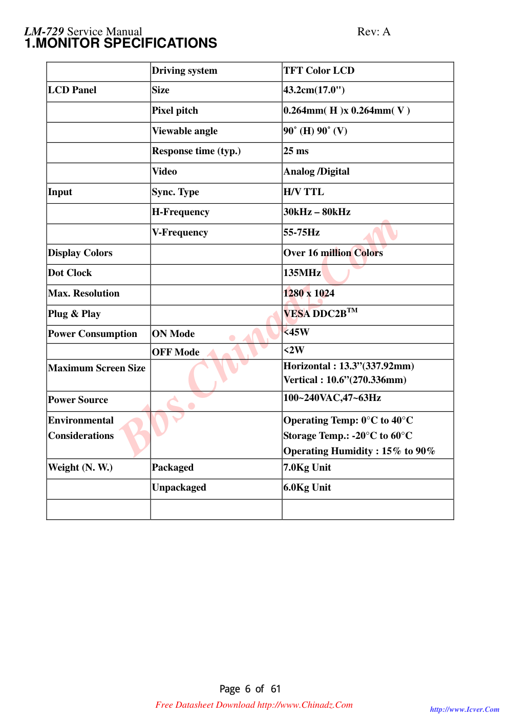
1.MONITOR SPECIFICATIONS
Driving system
TFT Color LCD
LCD Panel
Size
43.2cm(17.0")
Pixel pitch
0.264mm( H )x 0.264mm( V )
Viewable angle
90˚ (H) 90˚ (V)
Response time (typ.)
25 ms
Video
Analog /Digital
Input
Sync. Type
H/V TTL
H-Frequency
30kHz – 80kHz
V-Frequency
55-75Hz
Display Colors
Over 16 million Colors
Dot Clock
135MHz
Max. Resolution
1280 x 1024
Plug & Play
VESA DDC2BTM
Power Consumption
ON Mode
<45W
OFF Mode
<2W
Maximum Screen Size
Horizontal : 13.3”(337.92mm)
Vertical : 10.6”(270.336mm)
Power Source
100~240VAC,47~63Hz
Environmental
Considerations
Operating Temp: 0°C to 40°C
Storage Temp.: -20°C to 60°C
Operating Humidity : 15% to 90%
Weight (N. W.)
Packaged
7.0Kg Unit
Unpackaged
6.0Kg Unit
Free Datasheet Download http://www.Chinadz.Com
http://www.Icver.Com
Bbs.Chinadz.Com
LM-729 Service Manual Rev: A
Page 7 of 61
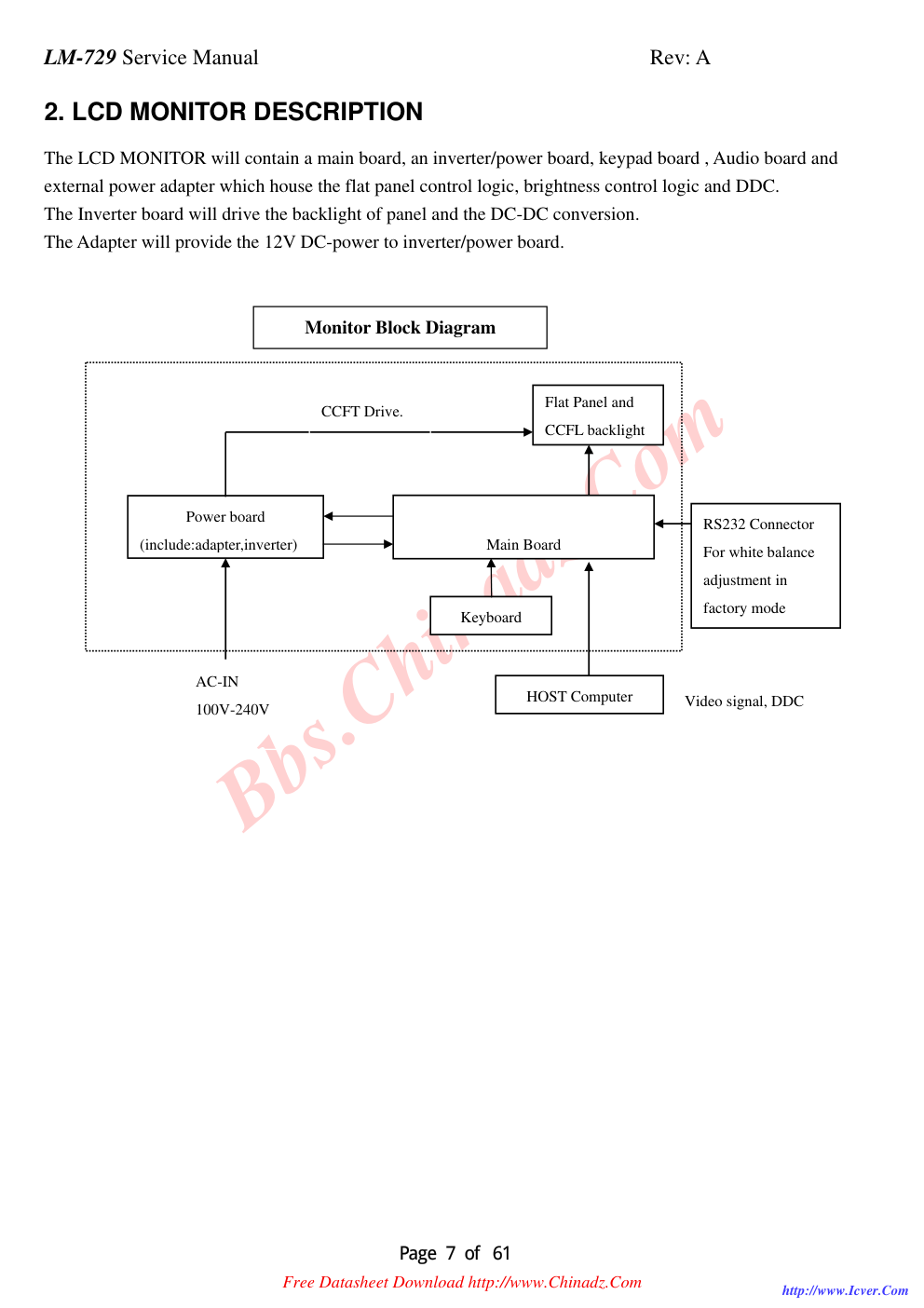
2. LCD MONITOR DESCRIPTION
The LCD MONITOR will contain a main board, an inverter/power board, keypad board , Audio board and
external power adapter which house the flat panel control logic, brightness control logic and DDC.
The Inverter board will drive the backlight of panel and the DC-DC conversion.
The Adapter will provide the 12V DC-power to inverter/power board.
Power board
(include:adapter,inverter)
Flat Panel and
CCFL backlight
Main Board
Keyboard
RS232 Connector
For white balance
adjustment in
factory mode
HOST Computer
CCFT Drive.
AC-IN
100V-240V
Video signal, DDC
Monitor Block Diagram
Free Datasheet Download http://www.Chinadz.Com
http://www.Icver.Com
Bbs.Chinadz.Com
LM-729 Service Manual Rev: A
Page 8 of 61
3. OPERATING INSTRUCTIONS
3.1 GENERAL INSTRUCTIONS
Press the power button to turn the monitor on or off. The other control buttons are located at front panel of the monitor. By
changing these settings, the picture can be adjusted to your personal preferences.
- The power cord should be connected.
- Connect the video cable from the monitor to the video card.
- Press the power button to turn on the monitor, the power indicator will light up.
3.2 CONTROL BUTTONS
- Power Button:
When pressed, the monitor enters the off mode, and the LED turns blank. Press again to restore normal status.
- Left / Right Button:
When the OSD show on screen, Left/Right Button are used to control the monitor functions. Press to switch functions or adjust
settings. And if the OSD off, Left/Right buttons are used to control the audio volume;
- Auto Adjust Key:
The Auto Adjust Key is used to automatically set the H Position, V Position, Clock and Phase.
- Power Indicator:
Green
— Power On mode.
Orange
— Power Saving mode.
Blank —Power Off Mode.
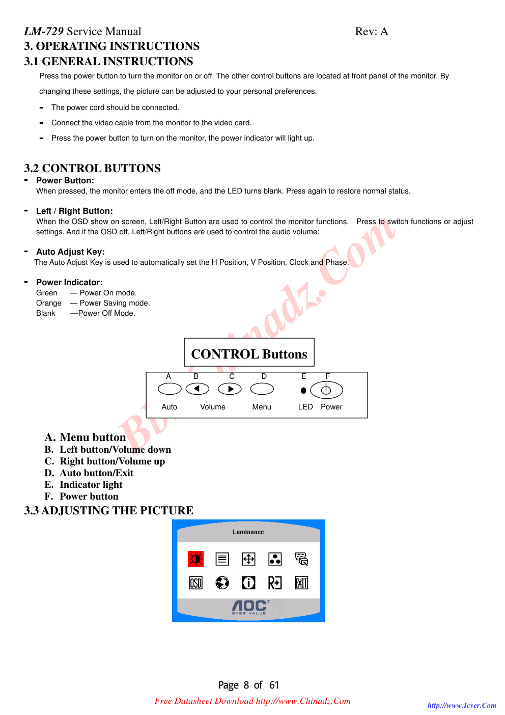
A B C D E F
Auto Volume Menu LED Power
A. Menu button
B. Left button/Volume down
C. Right button/Volume up
D. Auto button/Exit
E. Indicator light
F. Power button
3.3 ADJUSTING THE PICTURE
CONTROL Buttons
Free Datasheet Download http://www.Chinadz.Com
http://www.Icver.Com
Bbs.Chinadz.Com
LM-729 Service Manual Rev: A
Page 9 of 61
OSD Table:
Main
Menu Item
Main
Menu Icon
Sub Menu
Item
Sub
Menu
Icon
Description
Adjust
Range
Reset Value
Contrast
Contrast from Digital-register. 0-100 Recall Cool
Contrast Value
Luminance
Brightness
Backlight Adjustment
0-100 Recall Cool
Brightness Value
Focus
Adjust Picture Phase to reduce
Horizontal-Line noise
0-100 Do Auto Config
Image
Setup
Clock
Adjust picture Clock to reduce
Vertical-Line noise.
0-100 Do Auto Config
H. Position
Adjust the horizontal position
of the picture.
0-100 Do Auto Config
Image
Position
V. Position
Adjust the verticalposition of
the picture.
0-100 Do Auto Config
Warm
N/A
Recall Warm Color
Temperature from EEPROM.
N/A
Cool
N/A
Recall Cool Color
Temperature from EEPROM.
N/A
User / Red
Red Gain from
Digital-register.
0-100
User / Green
Green Gain Digital-register.
0-100
Color
Temp.
User / Blue
Blue Gain from
Digital-register.
0-100
The Color
Temperature will
be set to Cool.
The User R/G/B
value(default is
100) will not be
Modified by Reset
function.
Yes
N/A
Auto Adjust the H/V Position,
Focus and Clock of picture.
N/A
N/A
Auto
Config
(Analog-On
ly Model)
No
N/A
Do not execute Auto Config,
return to main menu.
N/A
N/A
Analog
N/A
Select input signal from analog
(D-Sub)
N/A
N/A
Input Select
(Dual-Input
Model)
Digital
N/A
Select input signal from digital
(DVI)
N/A
N/A
H. Position
Adjust the horizontal position
of the OSD.
0-100 50
V. Position
Adjust the verticalposition of
the OSD.
0-100 50
OSD Setup
OSD Timeout
Adjust the OSD timeout.
10-120 10
Free Datasheet Download http://www.Chinadz.Com
http://www.Icver.Com
Bbs.Chinadz.Com
LM-729 Service Manual Rev: A
Page 10 of 61
English
N/A
Set OSD display language to
English.
N/A
Deutsch
N/A
Set OSD display language to
German.
N/A
Français
N/A
Set OSD display language to
French.
N/A
Español
N/A
Set OSD display language to
Spain.
N/A
Italiano
N/A
Set OSD display language to
Italian.
N/A
Language
简体中文
N/A
Set OSD display language to
Simplified Chinese.
N/A
The Language will
be set to English.
Information
Information
N/A
Show the resolution, H/V
frequency and input port of
current iput timing.
N/A
N/A
Yes
N/A
Clear each old status of
Auto-configuration and set the
color temperature to Cool.
N/A
N/A
Reset
No
N/A
Do not execute reset, return to
main menu.
N/A
N/A
Exit
N/A
N/A
Exit OSD
N/A
N/A
Free Datasheet Download http://www.Chinadz.Com
http://www.Icver.Com
Bbs.Chinadz.Com
LM-729 Service Manual Rev: A
Page 11 of 61
4. Input/Output Specification
4.1 Input Signal Connector
4.1.1 Analog D-SUB Connector
PIN NO.
DESCRIPTION
PI N NO.
DESCRIPTION
1.
Red
9.
+5V
2.
Green
10.
Detect Cable
3.
Blue
11.
NC
4.
Ground
12.
DDC-Serial Data
5.
Ground
13.
H-Sync
6.
R-Ground
14.
V-Sync
7.
G-Ground
15.
DDC-Serial Clock
8.
B-Ground
VGA connector layout
1
5
6
10
11
15
4.1.2 DVI-D Connector
DVI-D Connector to be compliant to the latest DVI-DDWG specification version available.
Pin
Meaning
Pin
Meaning
Pin
Meaning
1
TMDS Data2-
9
TMDS Data1-
17
TMDS Data0-
2 TMDS Data2+
10
TMDS Data1+
18
TMDS Data0+
3 TMDS Data 2/4
Shield
11 TMDS Data 1/3 Shield
19
TMDS Data 0/5 Shield
4
not connected
12 not connected
20
not connected
5 not connected
13
not connected
21
not connected
6 DDC Clock
14 +5V Power
22
TMDS Clock Shield
7 DDC Data
15 Ground
23
TMDS Clock-
8 Analogue Vertical
Sync
16
Hot Plug Detect
24
TMDS Clock+
Free Datasheet Download http://www.Chinadz.Com
http://www.Icver.Com
Bbs.Chinadz.Com
LM-729 Service Manual Rev: A
Page 12 of 61
1
9
17
4.2 Factory Preset Display Modes
VESA MODES
Horizontal
Vertical
Mode
Resolution
Total
Nominal
Frequency
+/- 0.5kHz
Sync
Polarity
Nominal
Freq.
+/- 1 Hz
Sync
Polarity
Nominal Pixel
Clock
(MHz)
640x480@60Hz
800 x 525
31.469
N
59.940
N
25.175
640x480@72Hz
832 x 520
37.861
N
72.809
N
31.500
VGA
640x480@75Hz
840 x 500
37.500
N
75.00
N
31.500
800x600@56Hz
1024 x 625
35.156
N/P
56.250
N/P
36.000
800x600@60Hz
1056 x 628
37.879
P
60.317
P
40.000
800x600@72Hz
1040 x 666
48.077
P
72.188
P
50.000
SVGA
800x600@75Hz
1056x625
46.875
P
75.000
P
49.500
1024x768@60Hz
1344x806
48.363
N
60.004
N
65.000
1024x768@60Hz
1312x813
48.78
N
60.00
N
64.000
1024x768@70Hz
1328x806
56.476
N
70.069
N
75.000
1024x768@72Hz
1304x798
57.515
P
72.074
P
75.000
1024x768@75Hz
1328x804
60.200
N
74.90
N
80.000
XGA
1024x768@75Hz
1312x800
60.023
P
75.029
P
78.750
XGA
1152x864@75Hz
1600x900
67.50
P
75.000
P
108.000
1280x1024@60Hz
1688x1066
63.981
P
60.020
P
108.000
SXGA
1280x1024@75Hz
1688x1066
79.976
P
75.025
P
135.000
IBM MODES
Horizontal
Vertical
Mode
Resolution
Total
Nominal
Frequency
+/- 0.5kHz
Sync
Polarity
Nominal
Freq.
+/- 1 Hz
Sync
Polarity
Nominal
Pixel
Clock
(MHz)
DOS*
720x400@70Hz
900 x 449
31.469
N
70.087
P
28.322
DOS**
640x400@70Hz
800 x 449
31.469
N
70.087
P
25.175
MAC MODES
VGA
640x480@67Hz
864x525
35.000
N
66.667
N
30.240
SVGA
832x624@75Hz
1152x667
49.725
N
74.551
N
57.2832
Free Datasheet Download http://www.Chinadz.Com
http://www.Icver.Com
Bbs.Chinadz.Com
LM-729 Service Manual Rev: A
Page 13 of 61
4.3 Power Supply Requirements
4.3.1 Input Requirements
PARAMETER
RANGE
CONDITION
Input AC Voltage
100 to 240VAC RMS
Universal input full range
Input Frequency
60Hz @ 100VAC to 50Hz @
240VAC
Input Current
Less than 2.0 Amps RMS
Input voltage 100 VAC RMS ; 60 Hertz. Parameter
must be reached within 3 seconds of turn-on.
Less than 1.0 Amps RMS
Input voltage 220 VAC RMS ; 50 Hertz. Parameter
must be reached within 3 seconds of turn-on.
Input Power
Less than 75 Watts
Power factor > 0.5 Input voltage 120 VAC RMS ; 60
Hertz
Inrush Current
Less than 30 A peak
Input voltage 100 VAC RMS ; 60 Hertz at all
Phase(0, 90, 180, 270 degree)
Less than 50 A peak
Input voltage 240 VAC RMS ; 50 Hertz at all
Phase(0, 90, 180, 270 degree)
Input Fusing
Fuse should be located internal to the
adapter, easily accessible when the
cover is removed
Fuse must be UL/CSA approved. Fuse value must no
have to change for 115 VAC or 230 VAC operation
Leakage Current
Less than 3.5 mA
Input voltage 240 Volts RMS ; 50 Hertz
Hi-Pot
Primary to secondary
1.5KVAC for 1 Minute(leakage current 10mA)
1.8KVAC for 1 Minute(leakage current 10mA)
3.0KVAC for 1 Minute(leakage current 10mA)
without Y-cap & Coupling cap.
Prima1ry to Safety Ground
1.5KVAC for 1 Minute(leakage current 10mA)
1.8KVAC for 1 Minute(leakage current 10mA)
4.3.2 Output Requirements
PARAMETER
RANGE
CONDITION
DC Out
12VDC ± 5%
Min 0A Max 3.75A
Load Regulation
12.0V(12.12V) ± 5%
11.4 to 12.6VDC
Dynamic Load
Regulation
Any frequency up to 250Hz(duty
50%)
±5% for 10% to 100%, 100% to 10% load change for
+12Vdc
Ripple & noise
170mVpp at 12VDC
Input voltage : 100VAC at 60Hz 240VAC at 50Hz
* Ripple and noise are measured.
Output current
protection
less than 7.0A, more than 12.0A
at 12.0VDC
Current exceeds maximum rateing more than 20%
Leakage Current
Less than 0.25 mA
Input voltage 100 Volts RMS ; 50 Hertz
Less than 0.5 mA
Input voltage 240 Volts RMS ; 50 Hertz
Free Datasheet Download http://www.Chinadz.Com
http://www.Icver.Com
Bbs.Chinadz.Com
LM-729 Service Manual Rev: A
Page 14 of 61
4.4 PANEL SPECIFICATION
4.4.1 Panel Feature
-High contrast ratio, high aperture structure
-TN(Twisted Nematic) mode
-Wide viewing angle
-High speed response
-SXGA(1280 x 1024 pixels) resolution
-Low power consumption
-2 dual CCFTs(Cold Cathode Fluorescent Tube)
-DE(Data Enable) mode
-COMPACT SIZE DESIGN
4.4.2 Display Characteristics
Items
Specification
Unit
Display Area
337.92(H) x 270.336(V)
mm
Driver element
a-Si TFT active matrix
Display color
16.2M
Colors
Number of pixels
1280 x 1024
pixel
Pixel Arrangement
RGB vertical stripe
Pixel pitch
0.264(H) x 0.264(W)
mm
Display Mode
Normally White
4.4.3 Optical Characteristics
The optical characteristics are measured under stable conditions at 25℃ (Room Temperature):
Item
Symbol
Conditions
Min.
Typ.
Max.
Unit
Note
Contrast Ratio
(Center of screen)
C/R
250
450
-
Rising
Tr
-
4
5
Response
Time
Falling
Tf
-
12
20
msec
Luminance of White
(Center of screen)
YL
200
260
-
Cd/m2
Rx
0.64
Ry
0.34
Gx
0.29
Gy
0.61
Bx
0.14
By
0.07
Wx
0.31
Color
Chromaticity
(CIE 1931)
Coordinates (CIE)
Wy
Normal
ψ=0
θ=0
Viewing
Angl e
Typ.
-0.03
0.33
TYP.
+0.03
Brightness Uniformity
[%]
75
80
-
Free Datasheet Download http://www.Chinadz.Com
http://www.Icver.Com
Bbs.Chinadz.Com
LM-729 Service Manual Rev: A
Page 15 of 61
4.4.4 Parameter guide line for CCFL Inverter
INVERTER MAX BRINGTHNESS (Vadj:5.0v), LOAD=120KΩX4(ROOM TEMPERATURE 25℃ ±4℃)
ITEM
SYMBOL
MIN.
TYP.
MAX.
UNIT
REMARK
Input voltage
Vin
10.8
12
13.2
V
Input current
Iin
2250
2500
mA
FOR 4 LOAD
Output Current
Iout
6.0
6.5
7.0
mA
FOR 1 LOAD
Frequency
F
50.0
55.0
60.0
KHZ
FOR 1 LOAD
H.V open
Vopen
1450
1600
1750
Vrms
NO LOAD
H.V Load
Vload
710
810
910
Vrms
RL=120KΩ
Start voltage
Vst
1650
1750
1850
Vrms
RL=CCFL
Protect delay time
PDT
0.4
1
4
Sec
INVERTER MIN BRINGTHNESS (Vadj:0.0v), LOAD=120KΩX4(ROOM TEMPERATURE 25℃ ±4℃)
ITEM
SYMBOL
MIN.
TYP.
MAX.
UNIT
REMARK
input voltage
Vin
10.8
12
13.2
V
input current
Iin
660
750
mA
FOR 4 LOAD
Output Current
Iout
3.0
3.5
4.0
mA
FOR 1 LOAD
Frequency
F
50.0
55.0
60.0
KHZ
FOR 1 LOAD
H.V open
Vopen
1450
1600
1750
Vrms
NO LOAD
Start voltage
Vst
1650
1750
1850
Vrms
RL=CCFL
H.V Load
Vload
350
450
550
Vrms
RL=120KΩ
Free Datasheet Download http://www.Chinadz.Com
http://www.Icver.Com
Bbs.Chinadz.Com
LM-729 Service Manual Rev: A
Page 16 of 61
5. Block Diagram
5.1 Monitor Exploded View
Free Datasheet Download http://www.Chinadz.Com
http://www.Icver.Com
Bbs.Chinadz.Com
LM-729 Service Manual Rev: A
Page 17 of 61
5.2 Software Flow Chart
1
2
N
Y
5
Y
N
10
Y
N
12
Y
N
7
Y
N
6
4
3
8
9
14
11
13
Y
N
15
Y
N
16
17
19
Y
N
18
Free Datasheet Download http://www.Chinadz.Com
http://www.Icver.Com
Bbs.Chinadz.Com
LM-729 Service Manual Rev: A
Page 18 of 61
Remark:
1) MCU initialize.
2) Is the EEprom blank ?
3) Program the EEprom by default values.
4) Get the PWM value of brightness from EEprom.
5) Is the power key pressed ?
6) Clear all global flags.
7) Are the AUTO and SELECT keys pressed ?
8) Enter factory mode.
9) Save the power key status into EEprom.
Turn on the LED and set it to green color.
Scalar initialize.
10) In standby mode ?
11) Update the life time of back light.
12) Check the analog port, are there any signals coming ?
13) Does the scalar send out a interrupt request ?
14) Wake up the scalar.
15) Are there any signals coming from analog port ?
16) Display "No connection Check Signal Cable" message. And go into standby mode after
the message disappear.
17) Program the scalar to be able to show the coming mode.
18) Process the OSD display.
19) Read the keyboard. Is the power key pressed ?
Free Datasheet Download http://www.Chinadz.Com
http://www.Icver.Com
Bbs.Chinadz.Com
LM-729 Service Manual Rev: A
Page 19 of 61
5.3 Electrical Block Diagram
5.3.1 Main Board
OSD
Control
Interface
(CN9)
Scalar gm5126/gm2126
(Include MCU,ADC,OSD)
(U4)
Flash Memory
W39f010P-70B
(U6)
EEPROM
24C16
(U7)
D-Sub
Connector
(CN2)
EEPROM
24C02
(U2)
Hsync,
Vsync
RGB
RXD
TXD
DB15_SDA,
DB15_SCL
EPR_SDA
EPR_SCL
LCD
Interface
(CN4/CN5)
DVI-I only
Connector
(CN1)
EEPROM (D-I only)
24C02
(U1)
Free Datasheet Download http://www.Chinadz.Com
http://www.Icver.Com
Bbs.Chinadz.Com
LM-729 Service Manual Rev: A
Page 20 of 61
5.3.2 Inverter/Power Board
B uck C onnector
P arallet-resonant
D river
D im m ing control
(阀 菠 瓜 )
P arallet-resonant
inverter
C C FL
P W M
D im m ing con trol
D river
C ircuit
V in
V in
inverter
(P W M )
C ircuit
Inverter Block Diagram
Free Datasheet Download http://www.Chinadz.Com
http://www.Icver.Com
Bbs.Chinadz.Com
LM-729 Service Manual Rev: A
Page 21 of 61
PWPC7425A3
Power Block Diagram
Free Datasheet Download http://www.Chinadz.Com
http://www.Icver.Com
Bbs.Chinadz.Com
LM-729 Service Manual Rev: A
Page 22 of 61
6. Schematic
6.1 Main Board
GND
Bin
DDC_SCL_D1
DDC_SDA_A1
CN2
DB15
1
6
2
7
3
8
4
9
5
11
12
13
14
15
10
16
17
VGA_5V
AGND
AGND
RXC+
3
R8
100
1/16W
U3C
74LCX14
5
6
14
7
C20
NC
UART_DO
R40
47
1/16W
GND
VS
3
ZD5
MLL5232B 5.6V
D12
BAV99
3
1
2
RXC+IN
C17
0.1uF/16V
VGA_5V
R18
100
1/16W
75-ohm terminating resistor
very close to the VGA
conn.
Gin
+5V
C4
0.1uF/16V
D4
BAV99
3
1
2
R19
47
1/16W
D11
BAV99
3
1
2
ZD9
MLL5232B 5.6V
AGND
DDC_SCL_D
3
ZD7
MLL5232B 5.6V
AGND
GREEN+
3
R33
10K
1/16W
DIGITAL USE
GND
VGA_CONN
+5V
RX2+IN
C14
0.01uF/50V
ZD1
MLL5232B 5.6V
D3
BAV99
3
1
2
DVI_5V
R21
10K
1/16W
R38
47
1/16W
DDC_SCL_A
3
DDC_5V
ZD6
MLL5232B 5.6V
R3
10K
1/16W
AGND
BLUE+
3
DDC_SCL_A1
ZD2
MLL5232B 5.6V
R4
NC
2
DVI_5V
D10
BAV99
3
1
2
R13
NC
GND
C1
0.1uF/16V
gm5126
A
ANALOG&DIGITAL INPUT
AOC
C
2
8
星期二, 七月 22, 2003
Title
Size
Document Number
Rev
Date:
Sheet
of
AGND
DDC_SDA_D1
HS
3
(8 mil)
RX0+
3
C13
NC
+3V3
DDC_SCL_A1
R15
100
1/16W
R29
75
1/16W
GND
UART_DO
R28
47
1/16W
1
AGND
R26
0
1/16W
R43
NC
C19
NC
GREEN-
3
DDC_5V
R31
75
1/16W
U2
M24C02WMN6
4
8
1
2
3
7
6
5
GND
VCC
A0
A1
A2
WP
SCL
SDA
+5V
C6
0.1uF/16V
ADC_AGND
GND
C9
NC
C10
0.01uF/50V
AGND
DDC_SDA_D1
DDC_SDA_A1
C8
0.01uF/50V
R24
100
1/16W
Connect two grounds at one single point only.
+5V
C18
NC
RX0-
3
R11
10K
1/16W
RX0+IN
GND
DVI_PLUG
3
D7
BAV99
3
1
2
U3D
74LCX14
9
8
14
7
AGND
RX1+IN
RX2-IN
D5
BAV99
3
1
2
AGND
BLUE-
3
FB3
0
1/16W
AGND
RX1+
3
AGND
R14
NC
DVI_5V
R25
NC
SOT23
GND
C3
0.1uF/16V
RXC-
3
U3VCC
U3B
74LCX14
3
4
14
7
R17
100
1/16W
+5V
RX2+
3
+5V
GND
FB2
0
1/16W
ZD8
MLL5232B 5.6V
+5V
DDC_SDA_D
3
DDC_SCL_D1
R20
10K
1/16W
C12
0.1uF/16V
R35
2K
1/16W
D8
BAV99
3
1
2
R42
NC
AGND
UART_DI
ZD4
MLL5232B 5.6V
VGA_PLUG
AGND
GND
RX1-IN
R41
0
1/16W
R39
0
1/16W
HSin
GND
RX1-
3
6/24
U3A
74LCX14
1
2
14
7
HOT_PLUG
GND
C7
0.01uF/50V
D9
BAT54C-GS08
3
1
2
D2
BAV99
3
1
2
C16
NC
C5
0.1uF/16V
C21
NC
R32
4.7K 1/16W
GND
AGND
Rin
R30
75
1/16W
C2
0.1uF/16V
3
GND
RED+
3
UART_DI
AGND
FB1
0
1/16W
D1
BAV99
3
1
2
GND
GPIO5UART_DO
3
D6
BAV99
3
1
2
R16
100
1/16W
R5
100
1/16W
D13
BAT54C-GS08
3
1
2
Pins 6/7/8 are R/G/B
return lines resp.
DDC_SDA_A
3
RED-
3
VGA_PG
3
R2
47
1/16W
RX2-
3
GND
GPIO4UART_DI
3
R1
47
1/16W
CN1
1
2
3
4
5
6
7
8
9
10
11
12
13
14
15
17
18
19
20
21
23
24
C1
16
22
C2
C3
C4
27
25
26
T2-
T2+
SGND
T4-
T4+
DDCCLK
DDCDAT
A_VSYNC
T1-
T1+
SGND
T3-
T3+
+5V
GND
T0-
T0+
SGND
T5-
T5+
TC+
TC-
A_RED
HPD
SGND
A_GREEN
A_BLUE
A_HSYNC
A_GND
A_GND
A_GND
R34
2K
1/16W
+5V
R6
100
1/16W
R12
10K
1/16W
ADC_AGND
GND
RX0-IN
U1
M24C02WMN6
4
8
1
2
3
7
6
5
GND
VCC
A0
A1
A2
WP
SCL
SDA
GND
AGND
R10
100
1/16W
R27
100
1/16W
C11
0.01uF/50V
VSin
RXC-IN
ZD3
MLL5232B 5.6V
(10 mil, ┰ キ︽絬)
C15
0.01uF/50V
Free Datasheet Download http://www.Chinadz.Com
http://www.Icver.Com
Bbs.Chinadz.Com
LM-729 Service Manual Rev: A
Page 23 of 61
+3V3
ED02P
ED11N
ED21N
OD10N
TCON_ROE
1 = All 48K of ROM is in external ROM
GND
OD20P
4
C37
0.1uF/16V
RX0-
2
ED12P
4
ED00P
R65
10K
1/16W
+
C70
22uF/16V
DIGITAL PORT
RX0+
2
OD02N
4
OCLK_RS_N
RMADDR11
+
C49
22uF/16V
C65
0.1uF/16V
+3V3
+PV
OD11N
4
RMADDR8
R56
10K
1/16W
GPIO3
C54
0.1uF/16V
+3V3
GND
ED22P
4
ED20N
C50
0.1uF/16V
R46
4.7K
1/16W
If using 6-wire host protocol, program this bit to 0
RED+
2
ED21P
4
RMDATA3
C40
0.1uF/16V
X1
14.318MHz
1
2
C39
0.1uF/16V
TCON_OSP
4
ED22P
ED22N
C60
0.1uF/16V
C55
0.1uF/16V
SCLPOL
RMADDR12
RMDATA2
RMDATA4
+
C23
22uF/16V
STDBY
7
OD01N
3V3_RGB
R218
NC
U5 TCM809SENB713/NC
2
3
RST
VCC
GND
ED01N
4
GPIO2
SDA
RMADDR11
U4
GM5126
150
151
146
147
142
143
118
119
124
125
130
131
174
175
95
96
97
98
99
100
103
104
80
50
82
83
16
15
49
4
134
133
113
71
70
1
3
2
72
73
74
75
90
91
92
93
89
88
107
106
108
109
105
94
86
197
196
195
194
193
192
191
190
189
180
207
206
205
204
203
202
201
200
181
182
188
184
187
183
208
158
160
148
152
144
155
156
117
76
101
198
13
25
37
47
59
35
84
110
185
115
78
79
114
121
123
127
129
136
137
138
173
172
171
169
167
164
162
168
163
176
177
77
102
179
199
14
26
38
48
60
85
111
140
186
157
159
116
122
128
170
166
161
81
154
11
12
19
20
21
22
23
24
52
51
29
30
31
32
33
34
28
27
41
42
43
44
45
46
40
39
53
54
55
56
57
58
18
17
63
64
65
66
67
68
62
61
69
36
165
87
139
112
120
126
132
135
141
145
149
153
10
9
8
7
6
5
178
RED+
RED-
GREEN+
GREEN-
BLUE+
BLUE-
RX2+
RX2-
RX1+
RX1-
RX0+
RX0-
XTAL
TCLK
GPIO0/PWM0
GPIO1/PWM1
GPIO2/PWM2
GPIO3/TIMER1
GPIO4/UART_DI
GPIO5/UART_DO
GPIO6/TCON_SHC
GPIO7/TCON_TDIV
GPIO10/TCON_ROE3
OCLKP_RS
GPIO12/NVRAM_SDA
GPIO13/NVRAM_SCL
ECLKP_RS
ECLKN_RS
OCLKN_RS
DHS/TCON_LP
RXC-
RXC+
REXT
TCON_OPOL
TCON_OINV
TCON_ESP
TCON_EPOL
TCON_EINV
TCON_RSP2
TCON_RSP3
TCON_RCLK
TCON_ROE
GPIO20/HDATA3
GPIO19/HDATA2
GPIO18/HDATA1
GPIO17/HDATA0
GPIO16/HFS
GPIO22/HCLK
RESETn
GPIO21/TCON_FSYNC
GPIO14/DDC_SCL
GPIO15/DDC_SDA
GPIO9/TCON_ROE2
GPIO8/IRQINn
Reserved
ROM_ADDR0
ROM_ADDR1
ROM_ADDR2
ROM_ADDR3
ROM_ADDR4
ROM_ADDR5
ROM_ADDR6
ROM_ADDR7
ROM_ADDR8
ROM_ADDR15
ROM_DATA0
ROM_DATA1
ROM_DATA2
ROM_DATA3
ROM_DATA4
ROM_DATA5
ROM_DATA6
ROM_DATA7
ROM_ADDR14
ROM_ADDR13
ROM_ADDR9
ROM_ADDR11
ROM_ADDR10
ROM_ADDR12
ROM_OEn
VDD1_ADC_2.5
VDD2_ADC_2.5
AGND_GREEN
AGND_RED
AGND_BLUE
AGND_ADC
SGND_ADC
AGND_RX2
RVDD
RVDD
RVDD
EAVDD_RS_2.5
EAVDD_RS_2.5
AVDD_RS
OAVDD_RS_2.5
OAVDD_RS_2.5
CVDD_2.5
CVDD_2.5
CVDD_2.5
CVDD_2.5
VDD_RX2_2.5
PPWR
PBIAS
AGND_IMB
VDD_RX1_2.5
AGND_RX1
VDD_RX0_2.5
AGND_RX0
AGND_RXC
GND_RXPLL
VDD_RXPLL_2.5
AVDD_RPLL
AVSS_RPLL
VDD_DPLL
AVDD_DDDS
VDD_DDDS
AVDD_SDDS
VDD_SDDS
AVSS_DDDS
AVSS_SDDS
HSYNC
VSYNC
RVSS
RVSS
RVSS
RVSS
EAVSS_RS
EAVSS_RS
AVSS_RS
OAVSS_RS
OAVSS_RS
CVSS
CVSS
CLKOUT
CVSS
GND1_ADC
GND2_ADC
GND_RX2
GND_RX1
GND_RX0
VSS_DPLL
VSS_DDDS
VSS_SDDS
GPIO11/ROM_WEn
ADC_TEST
ECH3N_RS
ECH3P_RS
ECH5N_RS
ECH5P_RS
ECH6N_RS
ECH6P_RS
ECH7N_RS
ECH7P_RS
OCH4P_RS
OCH4N_RS
ECH9N_RS
ECH9P_RS
ECH10N_RS
ECH10P_RS
ECH11N_RS
ECH11P_RS
ECH8P_RS
ECH8N_RS
OCH1N_RS
OCH1P_RS
OCH2N_RS
OCH2P_RS
OCH3N_RS
OCH3P_RS
OCH0P_RS
OCH0N_RS
OCH5N_RS
OCH5P_RS
OCH6N_RS
OCH6P_RS
OCH7N_RS
OCH7P_RS
ECH4P_RS
ECH4N_RS
OCH9N_RS
OCH9P_RS
OCH10N_RS
OCH10P_RS
OCH11N_RS
OCH11P_RS
OCH8P_RS
OCH8N_RS
TCON_OSP
CVSS
N/C
Reserved
N/C
AVDD_IMB
AVDD_RX2
AVDD_RX1
AVDD_RX0
AVDD_RXC
AVDD_BLUE
AVDD_GREEN
AVDD_RED
AVDD_ADC
ECH2P_RS
ECH2N_RS
ECH1P_RS
ECH1N_RS
ECH0P_RS
ECH0N_RS
RVDD
GND
RMADDR0
RMDATA5
R64
10K
1/16W
1
Close to respective power Pins
OD00N
4
R219
0
1/16W
C45
0.1uF/16V
Determines polarity of HCLK signal
GND
GND
GPIO8
5
R49
NC
C33
0.1uF/16V
RX1-
2
TCON_ESP
+3V3
VS
2
OD01N
4
ED21N
4
SDA
OD01P
ED10N
4
OCLK_RS_P
HOST_PROTOCOL
+5V
TCON_LP
4
OD12N
4
GND
C31
0.1uF/16V
C59
0.1uF/16V
+5V
RMDATA1
R70
10K
1/16W
ROMCE
OD20P
C58
0.1uF/16V
C25
0.1uF/16V
VGA_PG
2
RMADDR13
Close to respective power Pins
ED01P
ED12N
DVI_PLUG
2
OD00P
gm5126
A
gm5126
AOC
C
3
8
星期二, 七月 22, 2003
Title
Size
Document Number
Rev
Date:
Sheet
of
ECLK_RS_P
4
ED02N
4
RMDATA6
GPIO7
C72
0.1uF/16V
BLUE-
2
ROM_WE
R61
NC
R222
NC
1
GND
+3V3
OD22P
4
C28
NAME
AGND
TCON_EPOL
4
BANK0
R60
NC
+3V3
RMADDR14
SCL
GPIO5UART_DO
2
ED20N
4
ED10N
RMADDR7
ECLK_RS_P
If using 6-wire host protocol, program this bit to 1
RMDATA6
+
C64
22uF/16V
GND
RMADDR4
C30
ROM_ADDR8
ROM_ADDR14
HS
2
RMADDR14
ROM_ADDR7
Available for reading from a status register
RMADDR9
3V3_DDDS
BANK1
OD22N
OD10P
ROM_OEn
R88
33
1/16W
x
1
GND
TCON_LP
RMADDR0
R69
0
1/16W
R63
NC
R48
NC
RMADDR6
C68
5pF/50V
FB8
600 OHM
GND
R92
33
1/16W
+PV
+2V5
RX1+
2
R62
NC
C79
22pF/NC
R224
NC
ED10P
4
ED01P
4
ED12P
RESET
RMDATA3
OD10P
4
x
+3V3
RX2+
2
RED-
2
DDC_SCL_D
2
ED00P
4
ED20P
ROM_ADDR6
ROM_ADDR(12:10)
+PV
ED01N
RMADDR5
C66 NC
R89
33
1/16W
GND
ED00N
4
RMADDR3
ED02N
OD11N
R225
10K
1/16W
R220
NC
RMADDR3
RMADDR7
FB4
600 OHM
R71
10K
1/16W
RXC+
2
OD00P
4
GPIO3
5
D14
LL4148
DDC_SDA_A
2
TCON_ESP
4
FB6
600 OHM
RMADDR8
C38
0.1uF/16V
ROM_ADDR13
GND
GND
GPIO2
5
GPIO6
R55
22
1/16W
+3V3
RMADDR12
x
PWM0
7
3V3_SDDS
RMDATA1
RMADDR12
R217
NC
C34
0.1uF/16V
ROM_ADDR5
x
GND
GND
TCON_RCLK
4
RMADDR8
RMADDR14
C43
0.1uF/16V
R51
1K
1/16W
Reserved
+PV
RMDATA0
USER_BITS(7:5)
RXC-
2
AGND
OD02P
+3V3
+PV
RMADDR10
RMADDR1
+
C36
22uF/16V
R223
0
1/16W
C24
0.1uF/16V
R54
22
1/16W
OCM_START
C61
0.1uF/16V
C53
0.1uF/16V
GND
R67
NC
GND
GREEN-
2
PBIAS
7
OD12N
+
C57
22uF/16V
OD00N
+
C48
22uF/16V
HOST_PORT_EN
0
OD21N
4
OD20N
4
RMDATA5
RMADDR11
FB18
600 OHM
RX2-
2
ED11N
4
ED10P
OD22P
3V3_DVI
RMADDR1
C46
0.1uF/16V
ADD DEN SIGNAL PIN 4/28
ECLK_RS_N
4
ED22N
4
OD10N
4
VOLUME
7
TCON_EPOL
OD12P
4
U6
W39F010P
3
29
28
4
25
23
26
27
5
6
7
8
9
10
11
12
21
20
19
18
17
15
14
13
24
31
32
1
16
2
30
22
A15
A14
A13
A12
A11
A10
A9
A8
A7
A6
A5
A4
A3
A2
A1
A0
DQ7
DQ6
DQ5
DQ4
DQ3
DQ2
DQ1
DQ0
OE
WE
VCC
NC
GND
A16
NC/A17
CE
R68
NC
DVI_PLUG
OD02N
R87
33
1/16W
FB7
600 OHM
TCON_ROE
4
C62
0.1uF/16V
C47
0.1uF/16V
C67
NC
R53
10K
1/16W
ED12N
4
OD21P
R59
0
1/16W
FLASH/ Prom-Jet Socket
GND
+2V5
GND
RMADDR5
TCON_RCLK
C29
R66
10K
1/16W
AGND
RMADDR15
R221
NC
C71
0.1uF/16V
OD22N
4
ROMCE
C41
0.1uF/16V
+
C35
22uF/16V
SET
OD20N
OCM_ROM_CFG(1)
GPIO6
5
TCLK
OD12P
FB10
600 OHM
+3V3
OD01P
4
FB9
600 OHM
0 = XTAL and TCLK pins are connected
BLUE+
2
GPIO4UART_DI
2
RMDATA7
TCON_OSP
C44
0.1uF/16V
1 = OCM becomes active after OCM_CLK is stable
DDC_SDA_D
2
RMADDR13
RMADDR9
USER_BITS(4:0)
GREEN+
2
ED11P
4
RMADDR2
DDC_SCL_A
2
OCLK_RS_P
4
OCLK_RS_N
4
BANK0
ROM_WE
RMADDR9
TCON_RSP2
C74
22pF/NC
C69
5pF/50V
1
RMADDR10
C27
OD02P
4
RMADDR2
C52
0.1uF/16V
C32
0.1uF/16V
C76
22pF/NC
0
GND
ED21P
XTAL
CTRLP12V
4
C42
0.1uF/16V
Available for reading from a status register
RMDATA2
OSC_SEL
+3V3
GND
ED02P
4
RMDATA4
C51
0.1uF/16V
RMADDR15
R47
NC
ED11P
RMDATA0
DESCRIPTION
ED20P
4
RMADDR10
ADDRESS
GPIO(22:16) is on "Host Port" pins
GND
R50
0
1/16W
U7
M24C16-MN6T
1
2
3
4
5
6
7
8
A0
A1
A2
VSS
SI
SCK
WP
VCC
32-Pin PLCC Socket
ROM_ADDR9
TCON_RSP2
4
GPIO7
5
RMADDR1
OD11P
RMADDR3
RMADDR0
C86
22pF/NC
PPWR
4
ECLK_RS_N
RMADDR4
Reset
Circuit
BOOTSTRAP SIGNALS
OD11P
4
LED_GRN
5
R52
22
1/16W
ROM_ADDR(4:0)
GPIO0/PWM0
ED00N
RMADDR2
FB19
600 OHM
GND
GND
OD21N
RMADDR6
RMADDR4
R57
10K
1/16W
FB5
600 OHM
+3V3
LED_ORANGE 5
BANK1
SCL
GND
OD21P
4
Free Datasheet Download http://www.Chinadz.Com
http://www.Icver.Com
Bbs.Chinadz.Com
LM-729 Service Manual Rev: A
Page 24 of 61
ED01P
3
OD22N
+12V
ED10N
3
R84
10K
PPWR
3
TCON_OSP
3
OD20N
OD22P
R79
NC
GND
ED20P
3
ED00N
3
ED22P
OD01N
3
GND
ED20N
3
ECLK_RS_N
OD11N
+
C75
100uF/16V
GND
TCON_LP
GND
TCON_ROE
3
R202 NC
ED12N
R85
3K 1/16W
OCLK_RS_P
3
OD12N
R76 0
1/16W
ECLK_RS_N
3
+
C78
150uF/16V
OD21N
3
GND
OD10N
3
TCON_ESP
OCLK_RS_N
3
OD22N
3
ED12P
R74 NC
GND
ED20P
+P3V3
OD10P
TCON_RSP2
3
ED10P
3
OD02N
R82
100K
1/16W
+P5V
ED02P
3
+
C73
100uF/16V
OD22P
3
ED20N
ED11P
OD01P
OD00N
3
ED21N
3
GND
TCON_RCLK
ED01P
OD21N
CONNECTOR for PANEL
FB11
NC
GND
ED10N
TCON_LP
3
OCLK_RS_P
ED10P
+P5V
OD02N
3
ED12N
3
ED00P
CN4
CONNECTOR 50P
1
2
3
4
5
6
7
8
9
10
11
12
13
14
15
16
17
18
19
20
21
22
23
24
25
26
27
28
29
30
31
32
33
34
35
36
37
38
39
40
41
42
43
44
45
46
47
48
49
50
OD02P
3
C77
100pF
ED00P
3
R73
0
1/16W
ED11P
3
R201
510K
1/16W
OD12P
3
+P3V3
OD00P
CN5
CONNECTOR 30P
1
2
3
4
5
6
7
8
9
10
11
12
13
14
15
16
17
18
19
20
21
22
23
24
25
26
27
28
29
30
PPWR
3
TCON_RSP2
C82
0.1uF/16V
OD10N
+3V3
OD20P
3
R86
3K 1/16W
R77
NC
TCON_EPOL
3
GND
OD12N
3
R72
0
1/16W
ED00N
ECLK_RS_P
3
ED22P
3
+5V
ED01N
OD20P
OD11N
3
TCON_ROE
FB12
220 OHM
R80
100K
1/16W
GND
ED01N
3
ED02P
ED21P
R81 NC
OD02P
ED22N
3
OCLK_RS_N
+12V
GND
ED22N
Q5
PMBS3904
3
2
1
TCON_ESP
3
ED21P
3
ED21N
OD21P
ED12P
3
OD11P
3
ED11N
3
R78
NC
gm5126
A
Panel Interface(RSDS)
AOC
B
4
8
星期二, 七月 22, 2003
Title
Size
Document Number
Rev
Date:
Sheet
of
OD20N
3
ECLK_RS_P
OD00N
Q1
PMBS3904
3
2
1
GND
+
C200
22uF/16V
OD11P
TCON_EPOL
Q2
SI9933ADY-T1
1
2
3
4
8
7
6
5
S1
G1
S2
G2
D1
D1
D2
D2
R75
0
1/16W
GND
R203
100K
1/16W
+
C205
150uF/16V
CTRLP12V
3
R83 NC
TCON_RCLK
3
ED02N
OD00P
3
GND
OD01N
ED02N
3
OD12P
R200
100K
1/16W
OD01P
3
ED11N
C80
0.1uF/16V
+12V
OD10P
3
OD21P
3
Free Datasheet Download http://www.Chinadz.Com
http://www.Icver.Com
Bbs.Chinadz.Com
LM-729 Service Manual Rev: A
Page 25 of 61
+2V5
GND
+12V
Brightness
GND
PWM0
CONNECTOR for
POWER/INVERTER
Board
GND
STDBY
3
FB17
600 OHM
+5V
R112
1K
1/16W
R113
4.7K
R115
4.7K
GND
R231
10K
1/16W
GND
PWM0
Brightness
GND
VOLUME
3
GND
GND
R230 10K
1/16W
+
C231
1uF/16V
+5V
R117
1K
R118
1.5K
1/16W
+12V
+
C230
1uF/16V
U9
AIC1084-33CE
3
1
2
VIN
ADJ
VOUT
+
C127
22uF/16V
Mute
CN11
PIN HEADER 2*6P
2
4
6
8
10
12
1
3
5
7
9
11
D20 LL4148
D21
LL4148
GND
C110
0.1uF/16V
+
C117
100uF/16V
gm5126
A
Power
AOC
B
7
8
星期二, 七月 22, 2003
Title
Size
Document Number
Rev
Date:
Sheet
of
+5V
CN601
6P PLUG R/A
1
2
3
4
5
6
+5V
GND
R232
10K 1/16W
R116
1K
1/16W
C119
0.1uF/16V
FB15
600 OHM
+5V
GND
Standby
R114
1K
1/16W
U8
AIC1084-33CE
3
1
2
VIN
ADJ
VOUT
GND
+ C120
100uF/16V
PBIAS
3
+
C111
100uF/16V
C124
0.1uF/16V
GND
+
C126
100uF/16V
BackLight
On/Off
+3V3
C121
0.1uF/16V
C125
0.1uF/16V
FB16
600 OHM
Free Datasheet Download http://www.Chinadz.Com
http://www.Icver.Com
Bbs.Chinadz.Com
LM-729 Service Manual Rev: A
Page 26 of 61
6.2 AUDIO Board
C215
1000 pF
GND
STANDBY
OUT_L
CN204
33L8022-3A-H FEMALE
1
2
3
C213
0.1uF
GND
MUTE
C206
0.47uF