先锋PIONEER DV-696AV-K电路图
 "先锋PIONEER DV-696AV-K电路图-0")
 "先锋PIONEER DV-696AV-K电路图-1")
 "先锋PIONEER DV-696AV-K电路图-2")
 "先锋PIONEER DV-696AV-K电路图-3")
 "先锋PIONEER DV-696AV-K电路图-4")
 "先锋PIONEER DV-696AV-K电路图-5")
 "先锋PIONEER DV-696AV-K电路图-6")
 "先锋PIONEER DV-696AV-K电路图-7")
 "先锋PIONEER DV-696AV-K电路图-8")
 "先锋PIONEER DV-696AV-K电路图-9")
ORDER NO.
PIONEER CORPORATION 4-1, Meguro 1-chome, Meguro-ku, Tokyo 153-8654, Japan
PIONEER ELECTRONICS (USA) INC. P.O. Box 1760, Long Beach, CA 90801-1760, U.S.A.
PIONEER EUROPE NV Haven 1087, Keetberglaan 1, 9120 Melsele, Belgium
PIONEER ELECTRONICS ASIACENTRE PTE. LTD. 253 Alexandra Road, #04-01, Singapore 159936
PIONEER CORPORATION 2006
DV-490V
DV-696AV-S
RRV3452
DVD PLAYER
DV-696AV-S
DV-696AV-K
THIS MANUAL IS APPLICABLE TO THE FOLLOWING MODEL(S) AND TYPE(S).
Model
Type
Power Requirement
Region No.
Remarks
DV-696AV-S
WYXZT5
AC220 to 240 V
2
DV-696AV-S
WVXZT5
AC220 to 240 V
2
DV-696AV-K
WYXZT5
AC220 to 240 V
2
DV-696AV-K
YXZTUR5
AC220 to 240 V
5
DV-696AV-S
YXZTUR5
AC220 to 240 V
5
For details, refer to "Important Check Points for Good Servicing" .
T-ZZR JULY 2006 printed in Japan
DV-696AV-S
2
1
2
3
4
1
2
3
4
C
D
F
A
B
E
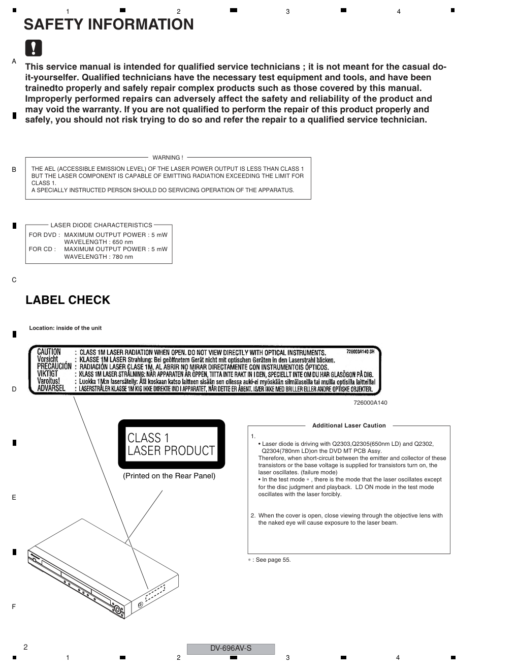
SAFETY INFORMATION
This service manual is intended for qualified service technicians ; it is not meant for the casual do-
it-yourselfer. Qualified technicians have the necessary test equipment and tools, and have been
trainedto properly and safely repair complex products such as those covered by this manual.
Improperly performed repairs can adversely affect the safety and reliability of the product and
may void the warranty. If you are not qualified to perform the repair of this product properly and
safely, you should not risk trying to do so and refer the repair to a qualified service technician.
WARNING !
THE AEL (ACCESSIBLE EMISSION LEVEL) OF THE LASER POWER OUTPUT IS LESS THAN CLASS 1
BUT THE LASER COMPONENT IS CAPABLE OF EMITTING RADIATION EXCEEDING THE LIMIT FOR
CLASS 1.
A SPECIALLY INSTRUCTED PERSON SHOULD DO SERVICING OPERATION OF THE APPARATUS.
LASER DIODE CHARACTERISTICS
FOR DVD : MAXIMUM OUTPUT POWER : 5 mW
WAVELENGTH : 650 nm
FOR CD :
MAXIMUM OUTPUT POWER : 5 mW
WAVELENGTH : 780 nm
Additional Laser Caution
∗ : See page 55.
726000A140
1.
• Laser diode is driving with Q2303,Q2305(650nm LD) and Q2302,
Q2304(780nm LD)on the DVD MT PCB Assy.
Therefore, when short-circuit between the emitter and collector of these
transistors or the base voltage is supplied for transistors turn on, the
laser oscillates. (failure mode)
• In the test mode ∗ , there is the mode that the laser oscillates except
for the disc judgment and playback. LD ON mode in the test mode
oscillates with the laser forcibly.
2. When the cover is open, close viewing through the objective lens with
the naked eye will cause exposure to the laser beam.
LABEL CHECK
(Printed on the Rear Panel)
Location: inside of the unit
DV-696AV-S
3
5
6
7
8
5
6
7
8
C
D
F
A
B
E
[Important Check Points for Good Servicing]
In this manual, procedures that must be performed during repairs are marked with the below symbol.
Please be sure to confirm and follow these procedures.
1. Product safety
Please conform to product regulations (such as safety and radiation regulations), and maintain a safe servicing environment by
following the safety instructions described in this manual.
1 Use specified parts for repair.
Use genuine parts. Be sure to use important parts for safety.
2 Do not perform modifications without proper instructions.
Please follow the specified safety methods when modification(addition/change of parts) is required due to interferences such as
radio/TV interference and foreign noise.
3 Make sure the soldering of repaired locations is properly performed.
When you solder while repairing, please be sure that there are no cold solder and other debris.
Soldering should be finished with the proper quantity. (Refer to the example)
4 Make sure the screws are tightly fastened.
Please be sure that all screws are fastened, and that there are no loose screws.
5 Make sure each connectors are correctly inserted.
Please be sure that all connectors are inserted, and that there are no imperfect insertion.
6 Make sure the wiring cables are set to their original state.
Please replace the wiring and cables to the original state after repairs.
In addition, be sure that there are no pinched wires, etc.
7 Make sure screws and soldering scraps do not remain inside the product.
Please check that neither solder debris nor screws remain inside the product.
8 There should be no semi-broken wires, scratches, melting, etc. on the coating of the power cord.
Damaged power cords may lead to fire accidents, so please be sure that there are no damages.
If you find a damaged power cord, please exchange it with a suitable one.
9 There should be no spark traces or similar marks on the power plug.
When spark traces or similar marks are found on the power supply plug, please check the connection and advise on secure
connections and suitable usage. Please exchange the power cord if necessary.
0 Safe environment should be secured during servicing.
When you perform repairs, please pay attention to static electricity, furniture, household articles, etc. in order to prevent injuries.
Please pay attention to your surroundings and repair safely.
2. Adjustments
To keep the original performance of the products, optimum adjustments and confirmation of characteristics within specification.
Adjustments should be performed in accordance with the procedures/instructions described in this manual.
4. Cleaning
For parts that require cleaning, such as optical pickups, tape deck heads, lenses and mirrors used in projection monitors, proper
cleaning should be performed to restore their performances.
3. Lubricants, Glues, and Replacement parts
Use grease and adhesives that are equal to the specified substance.
Make sure the proper amount is applied.
5. Shipping mode and Shipping screws
To protect products from damages or failures during transit, the shipping mode should be set or the shipping screws should be
installed before shipment. Please be sure to follow this method especially if it is specified in this manual.
DV-696AV-S
4
1
2
3
4
1
2
3
4
C
D
F
A
B
E
CONTENTS
SAFETY INFORMATION..................................................................................................................................... 2
1. SPECIFCATIONS ............................................................................................................................................. 5
2. EXPLODED VIEWS AND PARTS LIST ............................................................................................................ 6
2.1 PACKING SECTION .................................................................................................................................. 6
2.2 EXTERIOR SECTION................................................................................................................................ 8
2.3 06 DVD MECHA SECTION...................................................................................................................... 10
3. BLOCK DIAGRAM AND SCHEMATIC DIAGRAM.......................................................................................... 12
3.1 BLOCK DIAGRAM ................................................................................................................................... 12
3.2 OVERALL and POWER BLOCK DIAGRAM ............................................................................................ 14
3.3 OVERALL WIRING CONNECTION DIAGRAM........................................................................................ 16
3.4 DVD MT PCB ASSY (1/7) ........................................................................................................................ 18
3.5 DVD MT PCB ASSY(2/7) ......................................................................................................................... 20
3.6 DVD MT PCB ASSY(3/7) ......................................................................................................................... 22
3.7 DVD MT PCB ASSY(4/7) ......................................................................................................................... 24
3.8 DVD MT PCB ASSY(5/7) ......................................................................................................................... 26
3.9 DVD MT PCB ASSY(6/7) ......................................................................................................................... 28
3.10 DVD MT PCB ASSY(7/7) ....................................................................................................................... 30
3.11 OPERATION, OPERATION 2 and OPERATION 3, 4 PCB ASSYS ....................................................... 32
3.12 POWER PCB ASSY (1/2) ...................................................................................................................... 34
3.13 POWER PCB ASSY (2/2) ...................................................................................................................... 36
3.14 WAVE FORMS ....................................................................................................................................... 38
4. PCB CONNECTION DIAGRAM ..................................................................................................................... 41
4.1 LOADING and SW PCB ASSYS.............................................................................................................. 41
4.2 DVD MT PCB ASSY................................................................................................................................. 42
4.3 OPERATION, OPERATION 2 and OPERATION 3, 4 PCB ASSYS ......................................................... 46
4.4 POWER PCB ASSY................................................................................................................................. 50
5. PCB PARTS LIST ........................................................................................................................................... 52
6. ADJUSTMENT ............................................................................................................................................... 53
6.1 WHEN REPLACING DVD DECK ............................................................................................................. 53
6.2 TEST MODE ............................................................................................................................................ 54
6.3 TEST MODE IN........................................................................................................................................ 55
6.4 DISC REMOVAL METHOD...................................................................................................................... 56
7. GENERAL INFORMATION............................................................................................................................. 57
7.1 DIAGNOSIS ............................................................................................................................................. 57
7.1.1 DISPLAY SPECIFICATION OF THE TEST MODE............................................................................ 57
7.1.2 FUNCTIONAL SPECIFICATION OF THE SHORTCUT KEY ............................................................ 58
7.1.3 SPECIFICATION OF MODEL INFORMATION DISPLAY .................................................................. 59
7.1.4 FUNCTIONAL SPECIFICATION OF THE SERVICE MODE ............................................................. 60
7.1.5 METHOD FOR DIAGNOSING DEGRADATION OF THE LDS ON THE PICKUP ASSY .................. 61
7.1.6 TROUBLE SHOOTING...................................................................................................................... 62
7.2 DISASSEMBLY ........................................................................................................................................ 65
7.3 DVD DECK SECTION.............................................................................................................................. 66
7.4 IC INFORMATION.................................................................................................................................... 70
7.5 DISC / CONTENT FORMAT PLAYBACK COMPATIBILITY ..................................................................... 76
8. PANEL FACILITIES ........................................................................................................................................ 78
8.1 FRONT PANEL SECTION ....................................................................................................................... 78
8.2 REMOTE CONTROL ............................................................................................................................... 79
DV-696AV-S
5
5
6
7
8
5
6
7
8
C
D
F
A
B
E
1. SPECIFCATIONS
Specifications
General
System . . . . . . . . . . . . . . . . . . . . . . . DVD player
Power requirements
. . . . . . . . . . . . . AC 220 to 240 V, 50/60 Hz
Power consumption . . . . . . . . . . . . . . . . . . . 8 W
Power consumption (standby)
. . . . . . . . 0.8 W
Weight . . . . . . . . . . . . . . . . . . . . . . . . . . . . 1.7 kg
Dimensions
. . . .420 (W) mm x 49.5 (H) mm x 215.5 (D) mm
Operating temperature . . . . . . +5 °C to +35 °C
Operating humidity . . . . . . . . . . . . . 5 % to 85 %
(no condensation)
Component video output
Y (luminance) - Output level. . . . . . 1 Vp-p (75 Ω)
PB (color) - Output level . . . . . . . 0.7 Vp-p (75 Ω)
PR (color) - Output level . . . . . . . 0.7 Vp-p (75 Ω)
Jack
. . . . . . . . . . . . . . . . . . . . . . . . . . . . . . RCA
Video output
Output level . . . . . . . . . . . . . . . . . . . 1 Vp-p (75 Ω)
Jack . . . . . . . . . . . . . . . . . . . . . . . . . . . . . . . RCA
Audio output (1 stereo pair)
Output level
. . . . . . . . . . . . During audio output
200 mVrms (1 kHz, ± 20 dB)
Number of channels . . . . . . . . . . . . . . . . . . . . . 2
Jacks . . . . . . . . . . . . . . . . . . . . . . . . . . . . . . RCA
AV connector output
AV Connector (21-pin connector assignment)
AV connector output . . . . . . . 21-pin connector
This connector provides the video and audio
signals for connection to a compatible colour TV
or monitor.
PIN no.
1 . . . . . . . . . . . . . . . . . . . . . . . Audio 2/R out
3 . . . . . . . . . . . . . . . . . . . . . . . . . Audio 1/L out
4 . . . . . . . . . . . . . . . . . . . . . . . . . . . . . . . GND
7 . . . . . . . . . . . . . . . . . . . . . . . . . . . . . . . B out
8 . . . . . . . . . . . . . . . . . . . . . . . . . . . . . . Status
11 . . . . . . . . . . . . . . . . . . . . . . . . . . . . . . G out
15 . . . . . . . . . . . . . . . . . . . . . . . . . . . . . . R out
17 . . . . . . . . . . . . . . . . . . . . . . . . . . . . . . GND
19 . . . . . . . . . . . . . . . . . . . . . . . . . . . Video out
21 . . . . . . . . . . . . . . . . . . . . . . . . . . . . . . GND
HDMI output
HDMI output . . . . . . . . . . . . . . . . . . . . . . . .19 pin
Digital audio characteristics
Frequency response . . . . . . . . . . 4 Hz to 44 kHz
(DVD fs: 96 kHz)
S/N ratio . . . . . . . . . . . . . . . . . . . . . . . . . . . 115 dB
Dynamic range . . . . . . . . . . . . . . . . . . . . . . 100 dB
Total harmonic distortion . . . . . . . . . . . . 0.0025 %
Wow and flutter
. . . . . . . . Limit of measurement
(±0.001 % W. PEAK) or lower
Digital output
Coaxial digital output
. . . . . . . . . . . . . . .RCA jack
Optical digital output
. . . . . . .Optical digital jack
Accessories
Audio/video cable . . . . . . . . . . . . . . . . . . . . . . . .1
Power cable
. . . . . . . . . . . . . . . . . . . . . . . . . . .1
Remote control . . . . . . . . . . . . . . . . . . . . . . . . . .1
AA/R6P dry cell batteries
. . . . . . . . . . . . . . . . 2
Operating Instructions
The specifications and design of this product are subject to
change without notice, due to improvement.
Warranty card . . . . . . . . . . . . . . . . . . . . . . . . . . .1
S-video output
Y (luminance) - Output level . . . . . . 1 Vp-p (75 Ω)
C (color) - Output level
. . . 286 mVp-p (75 Ω)
Jack . . . . . . . . . . . . . . . . . . . . . . . . . . . . . S-video
Audio output (multi-channel / L, R, C, SW,
SL, SR)
Output level . . . . . . . . . . . . . During audio output
200 mVrms (1 kHz, ±20 dB)
Number of channels . . . . . . . . . . . . . . . . . . . . . 6
Jacks . . . . . . . . . . . . . . . . . . . . . . . . . . RCA jack
DV-696AV-S
6
1
2
3
4
1
2
3
4
C
D
F
A
B
E
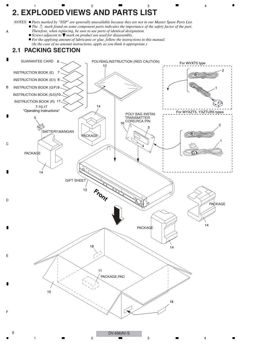
2. EXPLODED VIEWS AND PARTS LIST
2.1 PACKING SECTION
Parts marked by "NSP" are generally unavailable because they are not in our Master Spare Parts List.
The mark found on some component parts indicates the importance of the safety factor of the part.
Therefore, when replacing, be sure to use parts of identical designation.
Screws adjacent to mark on product are used for disassembly.
For the applying amount of lubricants or glue, follow the instructions in this manual.
(In the case of no amount instructions, apply as you think it appropriate.)
NOTES:
PACKAGE
GIFT SHEET
POLYBAG,INSTRUCTION (RED CAUTION)
PACKAGE
BATTERY,MANGAN
PACKAGE
PACKAGE
POLY BAG INSTA5
TRANSMITTER
CORD,RCA PIN
PACKAGE,PAD
15
14
18
18
3
4
14
13
For WVXT5 type
For WYXZT5, YXZTUR5 types
2
1
1
5
2
14
16
14
12
6
8
7
9
10
17
11
7-10,17
"Operating Instructions"
Front
INSTRUCTION BOOK (E/I)
INSTRUCTION BOOK (G/F)
INSTRUCTION BOOK (S/D)
INSTRUCTION BOOK (R)
GUARANTEE CARD
INSTRUCTION BOOK (E)
DV-696AV-S
7
5
6
7
8
5
6
7
8
C
D
F
A
B
E
PACKING SECTION parts List
(2) CONTRAST TABLE
DV-696AV-S/WVXT5, /YXZTUR5, DV-696AV-K/WYXZT5, /YXZTUR5 and DV-696AV-S/WYXZT5 are constructed
the same except for the following :
Mark No.
Description
Part No.
>
1
Cord Set AC
See Contrast table (2)
2
Cord, RCA Pin
06CPBA2006
3
Remote Control
07650KY040
4
Battery Cover
VNK4998
NSP 5
Battery,Mangan (AR, R6P)
• • • •
NSP 6
Guarantee Card
J2I80202A
7
Instruction Book
See Contrast table (2)
8
Instruction Book
See Contrast table (2)
9
Instruction Book
See Contrast table (2)
10
Instruction Book
See Contrast table (2)
11
Package, Pad
792WHA0604
12
Polyethylene Bag,Instruction
See Contrast table (2)
13
Gift Sheet
791WHA0100
14
Package
See Contrast table (2)
15
Gift Box
See Contrast table (2)
16
Poly, Bag
791WHAA040
17
Instruction Book
See Contrast table (2)
18
Carton Label
See Contrast table (2)
Mark No.
Description
Part No.
Mark No.
Symbol and Description
DV-696AV-S/
WYXZT5
DV-696AV-S/
WVXZT5
DV-696AV-S/
YXZTUR5
DV-696AV-K/
WYXZT5
DV-696AV-K/
YXZTUR5
>
1
Cord Set AC
1206158802
1206138802
1206158802
1206158802
1206158802
7
Instruction Book (English)
Not used
J2J00501B
Not used
Not used
Not used
8
Instruction Book (English, Italian)
J2J00321B
Not used
Not used
J2J00321B
Not used
9
Instruction Book (German, French)
J2J00322B
Not used
Not used
J2J00322B
Not used
10
Instruction Book (Spanish, Duch)
J2J00323B
Not used
Not used
J2J00323B
Not used
12
Polyethylene Bag,Instruction
JB5UD400
JB5UD200
JB5UD200
JB5UD400
JB5UD200
14
Package
792WHAA190
792WHAA191
792WHAA190
792WHAA190
792WHAA190
15
Gift Box
793WCD1748
793WCDD225
793WCD1748
793WCDD223
793WCDD223
17
Instruction Book (Russian)
Not used
Not used
J2J00601A
Not used
J2J00601A
18
Carton Label
Not used
Not used
723000D363
Not used
723000D365
DV-696AV-S
8
1
2
3
4
1
2
3
4
C
D
F
A
B
E
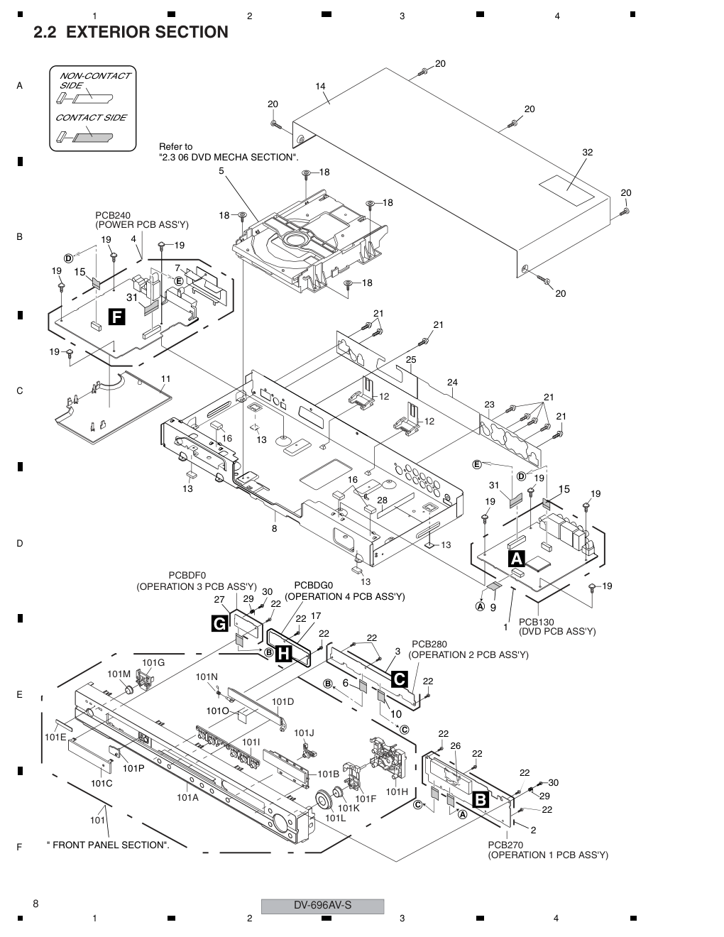
2.2 EXTERIOR SECTION
PCB240
(POWER PCB ASS'Y)
29
30
A
A
C
C
B
B
D
D
15
31
15
9
10
6
E
E
CONTACT SIDE
NON-CONTACT
SIDE
A
B
C
G
H
F
20
20
20
20
20
1
19
21
21
21
21
13
13
8
19
4
5
14
19
19
2
27
3
17
19
31
19
19
101C
22
22
22
22
26
22
22
22
11
13
13
16
19
18
18
18
18
23
24
25
(OPERATION 3 PCB ASS'Y)
PCB280
(OPERATION 2 PCB ASS'Y)
PCB270
(OPERATION 1 PCB ASS'Y)
PCB130
(DVD PCB ASS'Y)
101
101A
101E
101M
101G
101I
101D
101N
101J
101B
101K
101L
101F
101H
PCBDF0
12
12
16
PCBDG0
(OPERATION 4 PCB ASS'Y)
22
22
101O
101P
30
29
Refer to
"2.3 06 DVD MECHA SECTION".
" FRONT PANEL SECTION".
7
32
28
DV-696AV-S
9
5
6
7
8
5
6
7
8
C
D
F
A
B
E
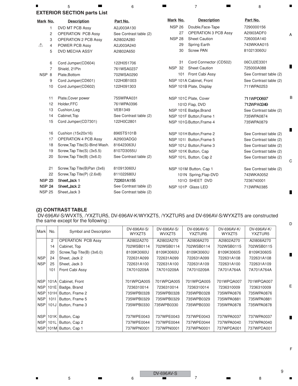
EXTERIOR SECTION parts List
(2) CONTRAST TABLE
DV-696AV-S/WVXT5, /YXZTUR5, DV-696AV-K/WYXZT5, /YXZTUR5 and DV-696AV-S/WYXZT5 are constructed
the same except for the following :
Mark No.
Description
Part No.
1
DVD MT PCB Assy
A2J003A130
2
OPERATION PCB Assy
See Contrast table (2)
3
OPERATION 2 PCB Assy
A2I802A280
>
4
POWER PCB Assy
A2J003A240
5
DVD MECHA ASSY
A2I802A650
6
Cord Jumper(CD604)
122H051706
7
Shield, 21Pin
761WSA0237
NSP 8
Plate,Bottom
702WSA0290
9
Cord Jumper(CD601)
122H0B1003
10
Cord Jumper(CD602)
122H091303
11
Plate,Cover power
755WPAA031
12
Holder,FFC
761WPA0396
13
Cushion,Leg
VEB1349
14
Cabinet,Top
See Contrast table (2)
15
Cord Jumper(CD7301)
122H0C2801
16
Cushion (15x20x16)
8965TS101B
17
OPERATION 4 PCB Assy
A2I903ADG0
18
Screw,Tap Tite(S)-Bind Wash.
816423063U
19
Screw,Tap Tite(S) (3x5.5)
8107D3055U
20
Screw,Tap Tite(B) (3x6.0)
See Contrast table (2)
21
Screw,Tap Tite(B)Pan (3x6)
810913060U
22
Screw,Tap Tite(P) (2.6x8)
811022680U
See Contrast table (2)
NSP 25
Sheet,Jack 3
See Contrast table (2)
NSP 26
Double,Face-Tape
7290000156
27
OPERATION 3 PCB Assy
A2I903ADF0
NSP 28
Sheet Caution
726000A140
29
Spring Earth
743WKAA015
30
Screw PAN
810213060U
31
Cord Connector (CD502)
06CU2E3301
NSP 32
Sheet Caution
725000A088
101
Front Cabi Assy
See Contrast table (2)
NSP 101A Cabinet, Front
See Contrast table (2)
NSP 101B Plate, Display
711WPA0253
NSP 101C Plate, Cover
101D Flap, DVD
NSP 101E Badge,Brand
See Contrast table (2)
NSP 101F Button,Frame 1
735WPA0874
NSP 101G Button,Frame 4
735WPA0879
NSP 101H Button,Frame 2
See Contrast table (2)
NSP 101I Button,Frame 5
See Contrast table (2)
NSP 101J Button,Frame 3
See Contrast table (2)
NSP 101K Button, Cap
See Contrast table (2)
NSP 101L Button, Cap 2
See Contrast table (2)
NSP 101M Button, Cap 1
See Contrast table (2)
101N Spring,Flap-DVD
743WKA0052
101O SHEET DVD
7236740001
NSP 101P Glass LED
713WPA0385
Mark No.
Description
Part No.
Mark
No.
Symbol and Description
DV-696AV-S/
WYXZT5
DV-696AV-S/
WVXZT5
DV-696AV-S/
YXZTUR5
DV-696AV-K/
WYXZT5
DV-696AV-K/
YXZTUR5
2
OPERATION PCB Assy
A2I802A270
A2I802A270
A2I808A270
A2I802A270
A2I808A270
14
Cabinet, Top
702WSB0114
702WSB0114
702WSB0114
702WSB0115
702WSB0115
20
Screw,Tap Tite(B) (3x6.0)
8109K3060U
8109K3060U
8109K3060U
8109K3060S
8109K3060S
NSP
24
Sheet, Jack 2
722631A099
722631A099
722631A099
722631A108
722631A108
NSP
25
Sheet, Jack 3
722631A100
722631A100
722631A109
722631A100
722631A109
101
Front Cabi Assy
7A7010209A
7A7010209A
7A7010209A
7A701A764A
7A701A764A
NSP 101A Cabinet, Front
701WPQA005
701WPQA005
701WPQA005
701WPQA007
701WPQA007
NSP 101E Badge, Brand
7236310014
7236310014
7236310014
7236310009
7236310009
NSP 101H Button, Frame 2
735WPB0328
735WPB0328
735WPB0328
735WPA0876
735WPA0876
NSP 101I
Button, Frame 5
735WPB0329
735WPB0329
735WPB0329
735WPA0881
735WPA0881
NSP 101J Button, Frame 3
735WPB0330
735WPB0330
735WPB0330
735WPA0878
735WPA0878
NSP 101K Button, Cap
737WPE0043
737WPE0043
737WPE0043
737WPA0037
737WPA0037
NSP 101L Button, Cap 2
737WPE0044
737WPE0044
737WPE0044
737WPA0040
737WPA0040
NSP 101M Button, Cap 1
737WPN0001
737WPN0001
737WPN0001
737WPDA001
737WPDA001
DV-696AV-S
10
1
2
3
4
1
2
3
4
C
D
F
A
B
E
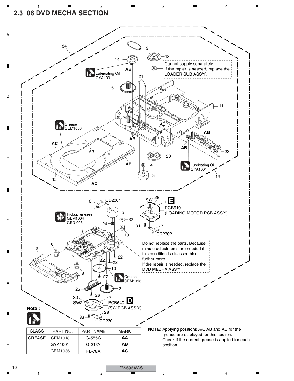
2.3 06 DVD MECHA SECTION
Applying positions AA, AB and AC for the
grease are displayed for this section.
Check if the correct grease is applied for each
position.
NOTE:
CLASS
MARK
GREASE
G-555G
AA
G-313Y
AB
PART NO.
GEM1018
PART NAME
GYA1001
FL-78A
AC
GEM1036
Cannot supply separately.
If the repair is needed, replace the
LOADER SUB ASS'Y.
PCB610
(LOADING MOTOR PCB ASS'Y)
CD2302
Do not replace the parts. Because,
minute adjustments are needed if
this condition is disassembled
further more.
If the repair is needed, replace the
DVD MECHA ASS'Y.
(SW PCB ASS'Y)
10
AB
AB
AB
AA
Pickup leneses
GEM1004
GED-008
Grease
GEM1018
34
15
14
21
18
11
23
9
AB
19
1
29
AB
AB
3
12
20
6
4
SW1
31
PCB640
27
22
22
16
2
CD2001
24
5
25
26
32
8
13
8
30
SW2
33
CD2301
AC
AC
AB
D
E
Lubricating Oil
GYA1001
Grease
GEM1036
Note :
Lubricating Oil
GYA1001
7
17
28
DV-696AV-S
11
5
6
7
8
5
6
7
8
C
D
F
A
B
E
06 DVD MECHA SECTION parts List
Mark No.
Description
Part No.
NSP 1
Loading Motor PCB Assy
A2F101A610
2
Gear,Middle
92P100117A
3
Loading Motor
1515S98004
4
Pulley,Motor
92P100097A
5
FEED Motor
1515S98004
6
Cord Jumper (24P)(CD2001)
122J402202
7
Cord Jumper (CD2302)
122H051602
8
Insulator (F)
92P200013A
9
Belt,Loading
92P200015A
10
Insulator (R)
92P200016A
11
Frame,main
92P100119A
12
Tray (B)
92P100127B
13
Holder ,Traverse
92P100125A
14
Gear,Pulley
92P100123A
15
Gear,Main
92P100124A
16
Gear,Feed
92P100116A
NSP 17
SW PCB Assy (PCB640)
A2F101A640
18
Plate, Clamper
92P000023A
19
LOADER SUB ASSY (B)
92AAA0019B
20
Clamper
92P100122A
21
Screw,Pan (M1.7x3 P3)
814011730U
22
Screw,Pan (M1.7x2.3 P3)
814011723U
23
Rack,Loading
92P100121A
24
Gear,Motor
92P100088A
25
Feed Rack Assy
92AAA0017A
26
Screw,T-Tite(B) (M1.7x5.0 P3)
813381750U
27
Screw,Gear Feed
92P700007A
28
Cord Jumper (CD2301)
122H061605
29
Switch (SW1)
0515S32003
30
Push Switch (SW2)
0500101036
31
Screw,Tap Tite(P) (2.6x8)
811022680U
32
Sems.Tap Tite(P) (2x8)
816112080U
33
Screw,Tap Tite(P) BI
811022080U
34
DVD MECHA ASSY
A2I802A650
DV-696AV-S
12
1
2
3
4
1
2
3
4
C
D
F
A
B
E
3. BLOCK DIAGRAM AND SCHEMATIC DIAGRAM
3.1 BLOCK DIAGRAM
D2+
1
3
D1+
4
D1-
6
D0+
7
D0-
9
CLK+
10
D2-
HDMI CONNECTOR
CP5901
DVD
Loader
(DM-4)
MPEG/MICON IC
IC4001
MT1389FE/E-L
X4001
27MHz
IOA, V20
C
RF, A, B, C, D, E, F, MDI1
LD_DVD, LD_CD
Q2302~2305
LD DRIVE
LDO1, LDO2
MOTOR DRIVER IC
IC2301
LA6565VR-TLM-E
DMSO, FMSO,
TROPEN, TRCLOSE,
TRSO, FOSO,
STBY, V1P4
T+/-, F+/-,
LOAD+/-,
MOT_SLED+/-,
MOT_SPDL+/-
OPU
SPINDLE/
STEPING/
SLED
MOTOR
LIMIT, TRIN, TROUT,
16Mbit FLASH
IC4004
S29AL016D70TFI020
MA0~MA11, DQ0~DQ15,
DQM0, DQM1, DBA0, DBA1,
SDCLK, SDCKE, DWE#,
DRAS#, DCAS#, DCS#
A
D
A0~A20, AD0~AD7,
PRD#, PCE#, PWR#
64Mbit SDRAM
IC4005
EM638165TS-7G
A
A
SDA
16
CLK-
12
HOTPLUG
19
POWER
18
15 SCL
HDMI TRANSMITTER IC
IC5901
MT1392E/C-L
SCL
SDA
92_Y0~Y7
92_VCK, 92_ACLK, XO
EEPROM IC
IC4002
BR24L08FJ-WE2
SCL
A
SDA
HDMI_SCL
HDMI_SDA
H
A, B
RESET IC
IC4003
BD5229G-TR
A
RESET
ASPDIF
DVD LOADER/MPEG BLOCK DIAGRAM
D2+
1
3
D1+
4
D1-
6
D0+
7
D0-
9
CLK+
10
D2-
HDMI CONNECTOR
CP5901
DVD
Loader
(DM-4)
MPEG/MICON IC
IC4001
MT1389EXE/B2-L
X4001
27MHz
IOA, V20
C
RF, A, B, C, D, E, F, MDI1
LD_DVD, LD_CD
Q2302~2305
LD DRIVE
LDO1, LDO2
MOTOR DRIVER IC
IC2301
LA6565VR-TLM-E
DMSO, FMSO,
TROPEN, TRCLOSE,
TRSO, FOSO,
STBY, V1P4
T+/-, F+/-,
LOAD+/-,
MOT_SLED+/-,
MOT_SPDL+/-
OPU
SPINDLE/
STEPING/
SLED
MOTOR
LIMIT, TRIN, TROUT,
16Mbit FLASH
IC4004
S29AL016D70TFI020
MA0~MA11, DQ0~DQ15,
DQM0, DQM1, DBA0, DBA1,
SDCLK, SDCKE, DWE#,
DRAS#, DCAS#, DCS#
A
D
A0~A20, AD0~AD7,
PRD#, PCE#, PWR#
64Mbit SDRAM
IC4005
EM638165TS-7G
A
A
SDA
16
CLK-
12
HOTPLUG
19
POWER
18
15 SCL
HDMI TRANSMITTER IC
IC5901
MT1392E/C-L
SCL
SDA
92_Y0~Y7
92_VCK, 92_ACLK, XO
ASPDIF
EEPROM IC
IC4002
BR24L08FJ-WE2
SCL
A
SDA
HDMI_SCL
HDMI_SDA
H
A, B
RESET IC
IC4003
BD5229G-TR
A
RESET
DVD LOADER/MPEG BLOCK DIAGRAM
DV-696AV-S
13
5
6
7
8
5
6
7
8
C
D
F
A
B
E
N IC
B2-L
A.......AT+3.3V
B.......+1.8V
C.......P.CON+5V
D.......P.CON+6V
E.......AT+12V
F.......P.CON+12V
G.......-28V
H.......V+5H
L
A
ESET IC
IC4003
5229G-TR
RESET
IR
IR RECEIVER (OS651)
ROM-N340TAO
IR
A
GR1~GR8, P1~P16
FP_DI, FP_DO,
FP_SCK, STB
FIP DRIVER IC
IC651
PT6315
A
FIP (V651)
HNV-08SS44T
G
A, B
IC8003/4/5
AUDIO DAC IC
PCM1742KEG/2K
DAC_XCSO, SCK, SD,ACLK,
ABCK, ALRCK, ASDAT0~2
1
COAXIAL JACK
J8102
COAXIAL
ASPDIF
1
OPTICAL
OS8001
OPTICAL
5
3
SL
C
LS/RS/S/LFE JACK
J8002
6
LFE
2
SR
A, C
IC8006/7/8
AUDIO LPF AND AMP IC
RC4580IDR
F
J8001
3
2
R
L
VIDEO DRIVER 6CH IC
IC7301
LA73054-TLM-E
LETTER, I/XP, S_Y, S_C,
R/CR, B/CB, G/Y, CVBS
3
5
Y
U
CVBS/Y/U/V
J7302
2
V
19 CVBS
21PIN CONNECTOR
J8101
11
15 R OUT
G OUT
16
7
B OUT
3
L
4CH BUS SW IC
IC7302
SN74CBT3257PWR
D
SQUEEZE, VSEL1
VSEL1
6
CVBS
CR OUT
Y OUT
CB OUT
1
R
8
VSEL1
SQUEEZE
21 PIN CTL
BLANKING_OUT
Q8101, Q8102
21 PIN CTL
Q8104, Q8105
DVD_RGB_H_OUT
S-VIDEO JACK
J7301
4
3
Y
C
C
L/R JACK
DV-696AV-S
14
1
2
3
4
1
2
3
4
C
D
F
A
B
E
3.2 OVERALL and POWER BLOCK DIAGRAM
P.CON+12V
AC220 V
- 240 V
FLDC+/-
27MHz
-28V
AT+12V for mute
AT+3.3V
P.CON+6V
P.CON+5V
POWER
SUPPLY
DVD LOADER
(DM4)
MOTOR DRIVER
IC2301
LA6565VR-TLM-E
FIP DRIVER IC
IC651
PT6315
8K EEPROM
IC4002
BR24L08FJ-WE2
FIP
HNV-08SS44T
KEY
SERVO
RF
SERVO
IR
FP,STB
RESET
LD_DVD,
LD_CD
IR
108MHz
TV Encoder
MPEG-1/2/
JPEG
VIDEO
DECORDER
RF
IR RECEIVER (OS651)
ROM-N340TAO
16Mbit FLASH
IC4004
S29AL016D70TFI020
64Mbit SDRAM
IC4005
EM638165TS-7G
SDA, SCL
MPEG/MICON BLOCK
IC4001
MT1389FE/E-L
AUDIO CODEC/
INTERNAL DAC
+1.8V
HDMI TRANSMITTER IC
IC5901
MT1392E/C-L
A0~A20,
AD0~AD7
MA0~MA11,
DQ0~DQ15
HDMI
CONNECTOR
CP5901
92_Y0~Y7,
92_VCK,
92_ACLK
TX0+/-,
TX1+/-,
TX2+/-,
TXC+/-
RESET IC
IC4003
BD5229G-TR
ASPDIF
AMUTE
VIDEO DRIVER 6CH IC
IC7301
LA73054-TLM-E
6CH VIDEO DAC
S_VIDEO
S
CVBS OUT
RGB OUT
CO
COAXIAL
OPTICAL
OP
IC8003/4/5
AUDIO DAC IC
PCM1742KEG/2K
DAC_XCSO, SCK, SD,
ACLK, ABCK, ALRCK,
ASDAT0~2
IC8006/7/8
AUDIO LPF AND AMP IC
RC4580IDR
C
LFE
SR
L
R
SL
21 PIN
CVBS
V
U
Y
4CH BUS SW IC
IC7302
SN74CBT3257PWR
• OVERALL BLOCK DIAGRAM
DV-696AV-S
15
5
6
7
8
5
6
7
8
C
D
F
A
B
E
SWITCHING
TRANS
T501
P.CON SW
• POWER BLOCK DIAGRAM
Q505
AC IN
P.CON+5V
AT+3.3V
FL DC -
-28V
AT+12V for mute
P.CON+6V
P.CON+12V
P.ON-H
FL DC +
Q515
P.CON +5V SW
Q510
P.CON +12V SW
Q504
FL+ P.CON SW
Q502
-28V P.CON SW
VOLTAGE CTL
IC501
KIA431A-AT
PHOTO COUPLER
IC504
PS2561AL1-1-V (W)
POWER CTL
IC502
STR-A6131M
6V REG
IC503
PQ070XF01SZH
REG+1.8V
IC4006
LM1117S-ADJ
+1.8V
HDMI+5V REG IC
IC5902
PQ1K503M2ZPH
V+5H
DV-696AV-S
16
1
2
3
4
1
2
3
4
C
D
F
A
B
E
3.3 OVERALL WIRING CONNECTION DIAGRAM
9
8
7
6
4
5
3
2
1
CP603
9
8
7
6
4
5
3
2
1
CP602
11
10
9
8
7
6
5
4
3
2
1
11
10
9
8
7
6
5
4
3
2
1
14
13
12
11
10
9
8
7
6
4
5
3
2
1
CP502
14
13
12
11
10
9
8
7
6
4
5
3
2
1
CP4003
5
4
3
2
1
CP605
5
4
3
2
1
CP604
Vout
B+
GND
OS651
1
2
3
2
1
AC220 V-240 V_50 Hz/60 Hz
CD501_2
AC INLET
J501
1
2
BLACK
WHITE
L
N
CP503_1
CP7301_1
N
L
CD7301
(CD502)
14
13
14
13
12
11
10
9
8
7
6
5
4
3
2
1
12
11
10
9
8
7
6
5
4
3
2
1
(CD604)
5
6
7
8
9
5
4
3
2
1
LED
V+3E
GND(NC)
POWER
SW2
(CD602)
5
6
7
8
9
5
4
3
2
1
LED
V+3E
GND(NC)
POWER
SW2
PAUSE/-SKIP
PLAY/+SKIP
V+3E
SW2
LED
GND
STOP
POWER
SW1
PAUSE/-SKIP
PLAY/+SKIP
V+3E
SW2
LED
GND
STOP
POWER
SW1
9
8
7
4
2
1
3
6
FLDC-
FLDC+
V+3E
-28V
DGND
DGND
DO (F to M)
DI (M to F)
IR
STB
CLK
DGND
DGND
FLDC+
-28V
FLDC-
DI (M to F)
V+3E
STB
DO (F to M)
IR
CLK
AT+3.3V
AT+3.3V
AT+3.3V
CP601
CP4002
P.CON+12V
P.CON+5V
FL DC-
FL DC+
GND
GND
AT+12V for MUTE
P.ON-H
P.CON+6V
-28V
GND(M)
GND(D)
GND
P.CON+5V
FL DC-
FL DC+
-28V
AT+3.3V
GND
P.CON+12V
AT+12V for MUTE
P.CON+6V
GND(M)
GND(D)
P.ON-H
D660
LTL-1CHEE-002A
HDMI LED(RED)
R664
330
1/4W
W808
W807
OPERATION 4 PCB ASSY
(A2I903ADG0)
H
12
11
10
9
8
7
6
5
4
3
2
1
12
11
10
9
8
7
6
5
4
3
2
1
J8101
21PIN CONNECTOR
1
10
11
12
13
14
15
16
17
18
19
2
20
21
3
4
5
6
7
8
9
NC
NC
NC
NC
NC
12
11
10
9
8
7
6
5
4
3
2
1
12
11
10
9
8
7
6
5
4
3
2
1
GND
AUDIO L
GND
AUDIO R
RGB-H
CVBS
FS
G
B
R
GND
GND
GND
GND
RGB-H
FS
GND
CVBS
GND
G
B
R
AUDIO L
AUDIO R
Vout
B+
GND
OS8101
1
2
3
H
E
J8102
COAXIAL
1
2
2
1
2
1
2
1
CP8102
2
1
CP8001
SPDIF
GND
SPDIF
GND
: POWER BLOCK
E 1/2
:D-TERMINAL/ AUDIO BLOCK
E 2/2
(CD601)
11
10
9
8
7
6
5
4
3
2
1
11
10
9
8
7
6
5
4
3
2
1
OPERATION PCB ASSY
(A2I802A270 : Other)
(A2I808A270 : YXZTUR5_Only)
B
OPERATION 2
PCB ASSY
(A2I802A280)
C
G
E 1/2, E 2/2
POWER PCB ASSY (A2J003A240)
AC IN
OPERATION 3 PCB ASSY
(A2I903ADF0)
DV-696AV-S
17
5
6
7
8
5
6
7
8
C
D
F
A
B
E
19
18
17
16
15
14
13
12
11
10
9
8
7
6
4
5
3
2
1
CP5901
HDMI CONNECTOR
H1
H2
E
H1
H2
E
J7302
CVBS/Y/U/V
1
2
3
4
5
6
H1
H2
E
J8001
AUDIO L/R
OUT
1
2
3
D2+
D2-S
D2-
D1+
D1-S
D0+
D0-S
D0-
CLK-S
CLK-
CEC
SCL
SDA
GND
POWER
HOTPLUG
NC
D1-
CLK+
LOADING MOTOR
SLED MOTOR
SPINDLE MOTOR
GND(SW)
SW-2(CLOSE)
SW-1(OPEN)
M2601
M
M
M
M2602
SW2
CD2301
CD2302
DVD MECHA ASSY
(A2I802A650)
D E
BCZ3B05
JCV9B12
ESE22MH22
BCZ3B05
M2603
SSS-28-5
SW1
5
4
3
2
1
CP2302
6
5
4
3
2
1
CP2303
24
23
22
21
20
19
2
1
18
17
16
15
14
13
12
11
10
9
8
7
6
5
4
3
CP2301
DM-4PB
LD-
LD-
LD+
LD+
OPEN
GND(D)
CLOSE
SW(GND)
SLD-
SLD+
SP1-
SP1+
LIMIT SW
SW(GND)
SLD-
SLD+
SP1-
SP1+
LIMIT SW
GND
VS
VCC
E
D
C
SW1(DVD/CD)
VRF(RF_OUT)
B
A
VR COM
VR(CD)
LD(CD)
LD(DVD)
GND
NC
T DRV
T RTN
F DRV
F RTN
F
VR(DVD)
GND
PD/GND
GND
VS
VCC
E
D
C
SW1(DVD/CD)
VRF(RF_OUT)
B
A
VR COM
VR(CD)
LD(CD)
LD(DVD)
GND
NC
T DRV
T RTN
F DRV
F RTN
F
VR(DVD)
GND
PD/GND
24
23
22
21
20
19
18
17
16
15
14
13
12
11
10
9
8
7
6
5
4
3
2
1
24
23
22
21
20
19
18
17
16
15
14
13
12
11
10
9
8
7
6
5
4
3
2
1
6
5
4
3
2
1
6
5
4
3
2
1
DRIVE
DVD
OPTICAL PICK-UP
LOADING MOTOR
PCB ASSY
(A2F101A610)
E
SW PCB ASSY
(A2F101A640)
D
H1
H2
E
H1
H2
E
J8002
LS/RS/C/U/LEF
1
2
3
4
5
6
J7301
S-VIDEO OUT
1
2
3
4
5
6
S-VIDEO OUT
DVD MT PCB ASSY (A2J003A130)
A 1/7- A 7/7
A
: MPEG/MICON/RF-AMP BLOCK
A 1/7
: LOADER/MOTOR DRV BLOCK
A 3/7
: MEMORY BLOCK
A 2/7
: AUDIO JACK BLOCK
A 4/7
: HDMI BLOCK
A 6/7
: VIDEO JACK BLOCK
A 5/7
: POWER PORT BLOCK
A 7/7
VIDEO OUT
AUDIO OUT
AUDIO OUT (5.1 ch)
÷ When ordering service parts, be sure to refer to "EXPLODED VIEWS and PARTS LIST" or
"PCB PARTS LIST".
÷ The > mark found on some component parts indicates the importance of the safety factor
of the part. Therefore, when replacing, be sure to use parts of identical designation.
÷
: The power supply is shown with the marked box.
DV-696AV-S
18
1
2
3
4
1
2
3
4
C
D
F
A
B
E
3.4 DVD MT PCB ASSY (1/7)
IC4002
MT1389EXE/B2-L
MPEG/MICON
222
223
224
225
226
227
228
229
230
231
232
233
234
235
236
237
238
239
240
241
242
243
244
245
246
247
248
249
250
251
252
253
254
255
256
1
10
11
12
13
14
15
16
17
18
19
2
20
21
22
23
24
25
26
27
28
29
3
30
31
32
33
34
35
36
37
38
39
4
40
41
42
43
44
45
46
47
48
49
5
50
51
52
53
54
55
56
57
58
59
6
60
61
62
63
64
65 66 67 68 69
7
70 71 72 73 74 75 76 77 78 79
8
80 81 82 83 84 85 86 87 88 89
9
90 91 92 93 94 95 96 97 98 99
R4008
10K
R4003
10K
R4005
680K
R4020
15K
R4027
100
R4035 33
R4014 10K
R4004 10K
R4006
10K
R4015
10K
R4016
15K
R4017
22K
R4018
12K
R4019
12K
R4002
10K
R4022
100K
R4030
10
R4024
750K
R4025
100K
TP4107
TP4009
TP4007
TP4001
TP4002
TP4003
TP4004
TP4005
TP4006
TP4008
TP4015
TP4016
TP4017
TP4018
TP4019
TP4020
TP4021
TP4030
TP4031
TP4032
TP4022
TP4023
TP4024
TP4025
TP4026
TP4027
TP4028
TP4029
TP4108
TP4109
TP4012
TP4013
TP4010
TP4011
TP4103
TP4014
TP4034
TP4033
TP4035
W881
C4026
0.1
B
C4012
0.1 B
C4105
0.0022 B
C4009
0.015 B
C4008
0.1 B
C4007
0.1
B
C4020
0.1
B
C4037
1
B
C4032
0.1 B
C4031
0.033 B
C4027
0.1 B
C4028
0.1
B
C4029
0.1
B
C4043
0.1
B
C4041
0.1
B
C4036
0.1 B
C4039
0.1
B
C4048
7P CH
C4050
0.1
B
C4013
0.1 B
C4014
1
B
C4015
1
B
C4016
1
B
C4001 0.0022 B
C4002
470P CH
C4022
0.1
B
C4003
470P CH
C4021 0.1 B
C4017
1
B
C4103
1
B
C4005
0.1
B
C4019
0.1
B
C4030
0.1
B
C4025
0.1
B
C4024 0.0015 B
C4051
0.1
B
C4042
0.047
B
C4044
0.047
B
C4040
1
B
C4033
0.001
B
C4049
7P
CH
C4045
0.47 B
C4034
22P CH
C4035
0.1 B
C4047
390P CH
IC4001
BR24L08FJ-WE2
EEPROM
1
2
3
4
5
6
7
8
C4023
220
6.3V
YK
C4046
10
25V
KA
X4001
100GT02720
27MHz
B4010
MMZ1608R102CT
OF PRINTING AND SUBJECT TO CHANGE WITHOUT NOTICE
NOTE:THIS SCHEMATIC DIAGRAM IS THE LATEST AT THE TIME
XO
V+3
ASPDIF
PWDN#
V1P4
A
B
C
D
E
F
MDI1
LDO1
LDO2
V1P4
DMSO
FMSO
TRCLOSE
TROPEN
TRSO
FOSO
OPO
OP+
OP-
TROUT
TRIN
D
STBY
A
V20
B
LIMIT
C
IOA
RF
RF
D_GND
E
F
MDI1
LDO2
LDO1
MA0
MA1
MA2
V20
MA3
V1P4
MA4
MA5
MA6
MA7
MA8
MA9
MA10
OPO
MA11
OP-
SDCKE
SDCLK
OP+
DBA0
DMSO
DBA1
FMSO
DCS#
TROPEN
DRAS#
DCAS#
DWE#
TRSO
DQM0
FOSO
DQM1
DQ0
V1P4
DQ1
DQ2
DQ3
DQ4
DQ5
DQ6
TROUT
DQ7
TRIN
DQ8
STBY
DQ9
TRCLOSE
DQ10
DQ11
DQ12
A2
DQ13
A3
DQ14
A4
DQ15
A0
A5
A1
A6
A2
A7
A3
A8
A4
A5
A18
A6
A19
A7
A8
A9
SDA
A10
SCL
A11
V+3
A12
A13
A14
A15
UWR#
URD#
A16
A17
A18
A19
A20
AD0
AD1
AD2
AD3
AD4
AD5
AD6
AD7
PWR#
A16
A15
A14
A13
A12
A11
A10
A20
PCE#
PRD#
AD0
AD1
AD2
AD3
AD4
AD5
AD6
AD7
A17
A9
A1
A0
PWR#
PCE#
PRD#
D_GND
FP_SCK
FP_DI
FROM/TO LOADER/MOTOR DRIVE
3.3
0.0
3.3
3.3
3.3V
1.8V
VCC
WP
SCL
SDA
NC
NC
NC
GND
(V+3D)
ADIN
IOCE#
IOWR#
3.3
NC
NC
NC
NC
NC
NC
NC
NC
NC
0.0
1.2
2.1
0.9
0.8
1.6
0.0
2.1
2.1
2.1
2.1
0.0
0.0
0.0
0.0
0.0
2.0
2.1
2.5
0.0
0.0
3.3
3.3
2.3
2.1
0.0
2.8
2.0
1.4
1.3
1.3
1.3
2.5
1.7
1.5
2.0
1.3
0.0
1.4
1.4
1.5
0.0
0.0
0.0
2.5
3.3
0.0
3.3
0.0
1.8
2.2
2.1
1.9
2.2
2.0
2.0
1.9
0.2
0.0
1.6
0.0
0.0
0.0
3.3
3.3
3.3
3.3
3.3
3.3
3.3
3.3
3.3
3.3
3.3
3.3
3.3
3.3
3.3
3.3
3.3
3.3
3.3
3.3
3.3
3.3
3.3
3.3
3.3
3.3
3.3
3.3
3.3
3.3
3.3
3.3
3.3
3.3
3.3
3.3
3.3
3.3
3.3
3.3
3.3
3.3
3.3
3.3
3.3
3.3
3.3
3.3
3.3
3.3
3.3
3.3
3.3
3.3
3.3
3.3
3.3
3.3
3.3
3.3
3.3
3.3
3.3
3.3
3.3
2.9
1.0
2.5
1.2
1.4
1.4
3.3
1.2
1.0
3.3
0.0
0.0
2.1
0.0
3.3
1.3
1.4
1.3
0.0
0.0
1.6
1.7
1.7
0.0
0.0
1.7
0.0
1.9
0.0
3.3
3.3
1.8
3.2
2.8
1.2
0.0
3.3
1.7
0.0
1.8
0.7
1.0
1.1
1.1
0.0
0.0
3.3
1.8
1.6
1.6
1.4
3.3
0.0
0.0
0.0
0.0
3.3
1.4
1.4
2.0
0.0
0.0
0.0
0.0
1.5
1.2
1.0
3.3
1.5
0.0
0.0
0.0
0.0
AGND
DVDA
DVDB
DVDC
DVDRF[P
DVDRF[N
MA
MB
MC
DVDD
SB
SC
SD
CDFON
CDFOP
TNI
SVDD3
SGND
V2REFO
V20
VFEFO
FEO
TEO
PWMOUT1/V_ADIN9
USBM
USB_VDD3
TDI/V_ADIN4 (JTAG)
FG/V_ADIN8 (PU)
TCK/V_ADIN6 (JTAG)
TDO/V_ADIN7 (JTAG)
IOA19 (PU)
IOA18 (PU)
65
66
67
68
254
253
255
256
A16
HIGHA7 (PU)
DVDD3
HIGHA2 (PU)
HIGHA3 (PU)
HIGHA4 (PU)
HIGHA5 (PU)
HIGHA6 (PU)
HIGHA1 (PU)
IOA20
XIOCS (PU)
DVDD3
AD0
AD1
AD2
AD3
DVSS (18)
AD4
AD5
AD6
ALE (PU)
AD7
A17
IOA0 (PU)
DVSS (3)
XUWR (PU)
XURD (PU)
DVDD18
UP1_2 (PU)
UP1_3 (PU)
MC_DATA (PD)
XTALI
JITFO
JITFN
RFRPDC
RFRPAC
HRFZC
CRTPLP
RFGND
CEQN
OSP
OSN
IREF
AVDD3
CSO/RFOP
TROPENPWM
TMS/V_ADIN5 (JTAG)
RFGC
SA
MD
TPI
LDO2
LDO1
OP_OUT
OP_INN
OP_INP
DMO
FMO
TRO
USBP
USB_VSS
DVDD18
IOA2 (PU)
IOA3 (PU)
IOA4 (PU)
IOA5 (PU)
IOA6 (PU)
HIGHA0 (PU)
APLLCAP
APLLVSS
DVSS
(PD) ASDATA4
(3) DVSS
SPDIF
RFGND18
RFVDD18
XTALO
PLLVSS
IDACEXLP
PLLVDD3
LPFON
LPFIP
LPFIN
LPFOP
ADCVDD3
S_VCM
ADCVSS
S_VREFP
S_VREFN
RFVDD3
CEQP
V+3RF
RFLV
FE
TE
FROM/TO MEMORY
FOO
MDI1
MDI2
RFLVL/RFON
TEZISLV
IOA7 (PU)
APLLVDD3
XIOWR
IOA1 (PU)
XIOOE
IOA21/V_ADIN0
CS
(RF)
(D)
(A)
(B)
(C)
(E)
(F)
(D)
(A)
(B)
(C)
(E)
(RF)
(RF)
(F)
1
EEPROM
3
7
8
A 1/7
2/7
A
3/7
A
DVD MT PCB ASSY (A2J003A130)
A 1/7
MPEG / MICON / RF-AMP BLOCK
DV-696AV-S
19
5
6
7
8
5
6
7
8
C
D
F
A
B
E
101102103104105106107108109110111112113114115116117118119120121122123124125126127128
129130131132133134135136137138139140141142143144145146147148149150151152153154155156157158159160161162163164165166167168169170171172173174175176177178179180181182183184185186187188189190191192
193
194
195
196
197
198
199
200
201
202
203
204
205
206
207
208
209
210
211
212
213
214
215
216
217
218
219
220
221
100
R4007
100
R4052
10K
R4038 33
R4040 33
R4043 33
R4050 33
R4047 33
R4046 10
R4083
100
R4070
33
R4071
33
R405410K
R4061
2.7K +-1%
R4062 15K
R4060
33
R4082
33
R4032
33
R4051
33
R4048
10K
R4053
10K
R4057
10K
R4084
1K
R4064
150+-1%
R4068
150+-1%
R4067
150+-1%
R4066
150+-1%
R4065
150+-1%
R4069
150+-1%
TP4053
TP4054
TP4055
TP4056
TP4057
TP4058
TP4059
TP4051
TP4052
TP4048
TP4106
TP4044
TP4043
TP4041
TP4039
TP4036
TP4037
TP4038
TP4063
TP4045
TP4076
TP4077
TP4078
TP4079
TP4080
TP4081
TP4082
TP4086
TP4087
TP4088
TP4085
TP4084
TP4083
TP4070
TP4071
TP4072
TP4075
TP4069
TP4073
TP4074
TP4110
TP4100
TP4101
TP4102
TP4095
TP4096
TP4097
TP4099
TP4098
TP4094
TP4060
TP4062
TP4061
TP4067
TP4066
TP4068
TP4046
TP4047
TP4050
TP4049
TP4089
TP4065
TP4040
TP4104
TP4042
TP4105
W805
W806
W846
W804
C4104
0.0082
B
C4053
0.1
B
C4114
1 B
C4055
0.1
B
C4073
0.1 B
C4072
0.1 B
C4068
0.1 B
C4062
0.1
B
C4064
0.1
B
C4069
100P CH
C4061
0.1
B
C4060
0.1
B
C4063
0.1
B
C4066
1
B
C4054
220P CH
C4076
33P CH
C4077
100P CH
C4078
33P CH
C4067
0.1 B
C4091
0.1 B
C4071
0.1
B
C4110
100P
CH
C4117
100P CH
C4079
100P CH
IC4003 BD5229G-TR
RESET IC
1
2
3
4
5
CP4002
00_6232_011_006_800+
1
10
11
2
3
4
5
6
7
8
9
NR4002
4D03WGJ0330T5E
NR4001
4D03WGJ0330T5E
NR4005
4D03WGJ0220T5E
NR4006
4D03WGJ0220T5E
DURING PLAYBACK.
MEASURED WITH THE DIGITAL TESTER
NOTE:THE DC VOLTAGE EACH PART WAS
IOA
SCK
ACLK
ABCK
G/Y
S_C
S_Y
ALRCK
XMMUTE
XAMUTE
HSYNC
VSYNC
R/CR
B/CB
V+3A
CVBS
ASDAT2
ASDAT1
ASDAT0
VSEL1
LETTER
SQUEEZE
I/XP
V+3V
R/CR
B/CB
G/Y
SD
CVBS
S_C
DAC_XCS0
S_Y
D_GND
SD
SCK
DAC_XCS0
XAMUTE
XMMUTE
VSEL1
ALRCK
ABCK
ACLK
LETTER
ASDAT0
SQUEEZE
ASDAT1
I/XP
ASDAT2
ASPDIF
D_GND
92_VCK
92_Y0
92_Y1
92_Y2
92_Y3
92_Y0
92_Y1
92_Y2
92_Y4
92_Y3
92_Y5
92_Y4
92_Y6
92_Y5
92_Y7
92_Y6
92_Y7
92_VCK
MA4
HDMI_SCL
MA5
HDMI_SDA
MA6
XO
URST#
MA7
HSYNC
VSYNC
MA8
MA9
MA11
SDCKE
PWDN#
SDCLK
V+1R8
V+3
V+3E
V+3A
FLDC-
FLDC+
MA3
-28V
MA2
D_GND
MA1
MA0
MA10
V+3
DBA1
RXD
DBA0
TXD
D_GND
DCS#
DRAS#
DCAS#
DWE#
DQS1
LIMIT
DQM1
DQ8
DQ9
FP_SCK
DQ10
FP_DI
DQ11
STB
DQ12
DQ13
FP_DO
IR
V+3E
FLDC+
-28V
FLDC-
DQ15
DQ14
DQM0
DQ7
DQ6
DQ5
DQ4
DQ3
DQ2
DQ1
DQ0
RESET
HDMI_SCL
HDMI_SDA
V+1R8
FP_DO
V+3
STB
SCL
SDA
RXD
TXD
IR
TO HDMI
FROM/TO POWER PORT
TO AUDIO/JACK
TO VIDEO
0
0
NC
NC
NC
NC
2.7
3.0
3.3
3.3
3.3
0.0
3.3
3.3
3.3
3.3
3.3
1.0
3.3
1.9
0.0
1.2
0.0
1.1
1.2
0.0
1.4
1.4
1.8
1.0
1.3
0.0
1.5
3.3
1.4
3.3
1.1
1.6
1.4
1.4
0.0
1.3
3.3
1.9
2.6
3.1
2.7
3.1
3.3
1.7
0.0
1.6
0.0
0.7
0.0
2.0
2.0
1.9
1.8
0.0
0.0
3.3
1.8
2.0
0.0
0.0
0.0
0.0
1.5
0.0
1.6
1.4
1.6
3.3
3.3
0.0
3.3
0.0
0.0
1.8
0.0
0.0
0.0
3.3
3.3
3.3
0.0
0.0
3.3
0.0
0.0
0.0
0.0
0.0
0.0
1.4
1.4
2.3
1.3
NC
NC
0.0
1.0
3.3
1.0
0.0
1.0
3.3
0.0
0.0
0.0
0.0
3.3
0.0
3.3
3.3
3.3
3.3
0.0
0.0
3.3
1.7
1.7
1.6
0.0
1.3
0.0
0.0
1.8
UP1_4 (PU)
UP1_5 (PU)
UP1_6 (PU)
UP1_7 (PU)
UP3_0 (PU)
UP3_1 (PU)
UP3_4 (PU)
PU3_5 (PU)
DVDD3
ICE (PD)
IR
DQM0
DQS0
RD7
DVSS (18)
RD6
125
126
127
128
RD5
DVSS (3)
RD4
RD3
DVDD18
RD2
RD1
RD0
RD15
RD14
RD13
RD12
RD11
RD10
RD9
(3) DVSS
DQS1
RD8
DQM1
XCAS
XRAS
DVDD3
XRCS
BA0
(18) DVSS
BA1
RA10
RA0
(3) DVSS
RA1
RA2
RA3
DVDD18
RCLKB
DVDD3
RCLK
RA11
RA9
RA8
(3)DVSS
RA7
(18) DVSS
RA6
RA5
RA4
DVDD3
(PU) RD30
RD29
RD28
RD27
DVDD18
RD26
(3) DVSS
RD25
RD24
(PD) DQM2
RD23
RD22
DVDD3
DACVSSC
DACVDDB
YUV3/CVBS
DACVDDA
DACVSSA
DVDD18
(PD) DQM3
DACVSSB
YUV5/B
YUV1/Y
XRWE
CKE
YUV6/R
DVDD3
YUV4/G
YUV2/C
(PD) ALRCK
ABCK
ACLK
DVDD3
SPLRCK
SPDATA
SPMCLK
YUV7/ASDATA5
(18) DVSS
(PD) ASDATA1
(PD) ASDATA2
(PD) ASDATA3
(PD) ASDATA0
(PD) RD21
(PD) RD20
(PD) RD19
(PD) RD18
(PD) RD17
(PD) RD16
INT0# (PU)
PRST# (PU)
0.0
NC
V+3D
1.8V
3.3V
(V+3D)
RVREF/V_ADIN3
(PU) RD31/ASDATA5
VSYNC/V_ADIN1
HSYNC/V_ADIN2
DACVDDC
VREF
FS
192
191
190
189
YUV0/CIN
SPBCK/ASDATA5
RESET
FROM/TO DISRLAY
(CP601)
DVDD3
1.8
NC
V_OUT
VSS
NC
CT
VDD
3.3
3.3
STB
DGND
DGND
FLDC+
-28V
FLDC-
CLK
DI(M to F)
DO(F to M)
IR
V+3E
: VIDEO SIGNAL ROUTE
(RF)
: RF SIGNAL ROUTE
(SY)
: S VIDEO SIGNAL ROUTE (Y)
(SC)
: S VIDEO SIGNAL ROUTE (C)
(R/CR)
: VIDEO SIGNAL ROUTE (R/CR)
(G/Y)
: VIDEO SIGNAL ROUTE (G/Y)
(B/CB)
: VIDEO SIGNAL ROUTE (B/CB)
(D)
: AUDIO DATA SIGNAL ROUTE
(DA)
: AUDIO SIGNAL ROUTE (Digital)
(R/CR)
(G/Y)
(B/CB)
(R/CR)
(G/Y)
(B/CB)
4
6
2
5/7
A
6/7
A
4/7
A
7/7
A
CP601
B
A 1/7
DV-696AV-S
20
1
2
3
4
1
2
3
4
C
D
F
A
B
E
3.5 DVD MT PCB ASSY(2/7)
A 2/7
DVD MT PCB ASSY (A2J003A130)
A 2/7
MEMORY BLOCK
1/7
A
1/7
A
7/7
A
DV-696AV-S
21
5
6
7
8
5
6
7
8
C
D
F
A
B
E
S29AL016D70TFI020
16Mbit FLASH IC
A 2/7
OF PRINTING AND SUBJECT TO CHANGE WITHOUT NOTICE
NOTE :THIS SCHEMATIC DIAGRAM IS THE LATEST AT THE TIME
DURING PLAYBACK.
MEASURED WITH THE DIGITAL TESTER
NOTE : THE DC VOLTAGE EACH PART WAS
DV-696AV-S
22
1
2
3
4
1
2
3
4
C
D
F
A
B
E
3.6 DVD MT PCB ASSY(3/7)
CP2301
LD07T2-24ND-03
PICK-UP(GOLD)
1
10
11
12
13
14
15
16
17
18
19
2
20
21
22
23
24
3
4
5
6
7
8
9
CP2302
00_6232_005_006_800+
LOADING
1
2
3
4
5
Q2301
KTC3875S_Y_RTK
VCR_CTL
CP2303
00_6232_006_006_800+
SLED/SPINDLE
1
2
3
4
5
6
S
D
G
Q2306
2SK3018T106
VCR_CTL
S
D
G
Q2307
2SK3018T106
VCR_CTL
IC2301
LA6565VR-TLM-E
MOTOR DRIVER
1
2
3
38
39
4
40
41
42
43
44
5
6
7
C2302
0.1
B
C2303
0.1
B
C2301
0.1
B
C2323
0.1
B
C2322
0.0022
B
C2313
0.01
B
C2312
1B
C2314
1B
R2308
10K
R2307
100K
R2309
10K
R2306
100K
R2341
10K
R2343
10K
R2338
10K
R2319
150K
R2329
1
R2342
680K
R2331
150K
R2310
2.7K
R2337
5.6K
R2311
10K
R2312
10K +-1%
R2313
10K +-1%
TP2304
TP2305
TP2306
TP2309
TP2310
TP2311
TP2312
TP2313
TP2314
TP2315
TP2316
TP2317
TP2318
TP2319
TP2308
TP2307
TP2320
TP2321
TP2322
TP2323
TP2302
JG002
JG003
JG004
JG005
JG006
JG007
TP2324
TP2325
TP2326
TP2327
TP2328
TP2303
JG001
TP2329
W864
W865
IOA
V+5S
V+5S
F
V20
E
D
C
IOA
RF
B
A
MDI1
T+
T-
F+
F-
TRSO
LOAD-
LOAD+
TROUT
V+6A
TRIN
V+3F
OPO
OP-
OP+
LIMIT
MOT_SLED-
MOT_SLED+
MOT_SPDL+
MOT_SPDL-
V+3F
TRCLOSE
TROPEN
LOAD-
LOAD+
T-
LOAD+
LOAD-
GND
OPEN
CLOSE
NC
0.0
4.9
0.0
0.0
0.2
5.0
0.0
0.0
0.0
SW(GND)
LIMIT SW
SLD-
SLD+
SPD-
SPD+
VRCOM
TRKG DRV
TRKG RTN
FOCS RTN
FOCS DRV
VCC
D
B
VR780(CD)
VRF(RF_OUT)
SW1(DVD/CD)
C
E
VS
F
GND
A
VR650(DVD)
GND
GND
LD_DVD(650)
LD_CD(780)
PD/GND
NC
FWD
REV
VCC2
VLD-
VLD+
VD4+
VIN4
VIN4-
MUTE234
MUTE1
VCONT
S-GND
0.0
4.0
3.3
3.3
TRACK
1.4
1.4
NC
0.0
5.9
0.1
0.0
0.8
2.6
NC
(F)
(F)
(E)
(E)
(D)
(D)
(C)
(C)
(B)
(B)
(RF)
(RF)
(A)
(A)
A 3/7
To PICKUP
DVD PCB ASSY (A2J003A130)
A 3/7
LOADER/MOTOR DRIVE BLOCK
CD2302
E
CD2301
D
MOTOR DRIVER
DV-696AV-S
23
5
6
7
8
5
6
7
8
C
D
F
A
B
E
Q2304
KTA1504S_Y_RTK
LD DRIV for CD
Q2305
KTA1504S_Y_RTK
LD DRIV for DVD
Q2302
KTA1504S_Y_RTK
LD DRIV for CD
Q2303
KTA1504S_Y_RTK
LD DRIV for DVD
10
11
12
13
14
15
16
17
18
19
20
21
22
23
24
25
26
27
28
29
30
31
32
33
34
35
36
37
8
9
C2305
0.1 B
C2311
0.01 B
C2310
0.01 B
C2307
1B
C2309
0.1 B
C2308
0.1
B
C2320
100
10V
YK
C2321
100
10V
YK
C2306
100
10V
YK
R2316
10K+-1%
R2328
10K+-1%
R2330
10K+-1%
R2322
4.7
R2320
4.7
R2323
4.7
R2321
4.7
R2327
4.7K
R2326
4.7K
R2318
10K +-1%
R2317
10K +-1%
R2325
15K +-1%
R2335
2.2
R2334
2.2
R2332
1.2
R2333
1.2
TP2336
TP2333
TP2334
TP2332
TP2341
JG010
JG008
TP2342
JG009
TP2339
TP2330
TP2338
TP2337
W807
NOTE : THIS SCHEMATIC DIAGRAM IS THE LATEST AT THE TIME
OF PRINTING AND SUBJECT TO CHANGE WITHOUT NOTICE
V20
A
B
C
D
E
V+3F
F
MDI1
LDO2
LDO1
IOA
V1P4
LDO1
LIMIT
TROUT
TRIN
STBY
DMSO
FMSO
TRCLOSE
TROPEN
TRSO
FOSO
LDO2
OPO
OP+
OP-
RF
V+3F
V+5S
FOSO
V+6A
D_GND
M_GND
STBY
DMSO
V1P4
FMSO
MOT_SPDL-
MOT_SPDL+
MOT_SLED-
MOT_SLED+
T+
F-
F+
FROM POWER PORT
FROM/TO MPEG/MICON/DSP
3.3
0
3.3
0
3.3
3.3
3.1
2.5
2.5
3.1
2.0
2.0
CD
DVD
RF33
VD4-
VD3+
VD3-
VD2+
VD2-
VD1-
VD1+
VCC1
VCCS
VIN1+A
VIN1-A
VIN 1
VIN3
VIN3-
VIN2
VIN2-
VIN2+
REG-OUT
VREF-OUT
VREF-IN
NC
PGND1
PGND2
VC2
1.4
NC
NC
NC
REG-IN
0.0
NC
VO_OP
VIN-OP
VIN+OP
NC
NC
NC
NC
1.4
1.4
1.1
FOCUS
1.4
1.4
2.5
2.5
2.6
0.0
0.0
2.7
2.5
5.9
5.9
1.4
1.4
1.4
3.9
1.4
NC
SPINDLE
SLED
THE DC VOLTAGE EACH PART WAS
MEASURED WITH THE DIGITAL TESTER
DURING PLAYBACK.
NOTE :
(RF)
: RF SIGNAL ROUTE
(A)
(RF)
(B)
(C)
(D)
(E)
(F)
18
1/7
A
7/7
A
A 3/7
DV-696AV-S
24
1
2
3
4
1
2
3
4
C
D
F
A
B
E
3.7 DVD MT PCB ASSY(4/7)
Q8006
KRC407-RTK/P
MUTE CTL
Q8009
KRC407-RTK/P
MUTE CTL
Q8004
KRC407-RTK/P
MUTE CTL
Q8003
KRC407-RTK/P
MUTE CTL
Q8007
KRC407-RTK/P
MUTE CTL
Q8002
KRC407-RTK/P
MUTE CTL
Q8020
KRC407-RTK/P
MUTE CTL
IC8003
PCM1742KEG/2K
AUDIO DAC (L,R)
1
10
11
12
13
14
15
16
2
3
4
5
6
7
8
9
IC8005
PCM1742KEG/2K
AUDIO DAC (Ls,Rs)
1
10
11
12
13
14
15
16
2
3
4
5
6
7
8
9
IC8004
PCM1742KEG/2K
AUDIO DAC (C,Lfe)
1
10
11
12
13
14
15
16
2
3
4
5
6
7
8
9
D8004
1SS355
D8005
1SS355
D8006
1SS355
D8003
UDZS6.8B
CP8001
A2001WV2-2P
1
2
Q8008
KTC3875S_Y_RTK
REF GEN
Q8012
KTC3875S_Y_RTK
REF GEN
Q8011
KTC3875S_Y_RTK
REF GEN
Q8005
KTC3875S_Y_RTK
REF CTL
Q8014
KTA1504S_Y_RTK
MUTE CTL
Q8013
KTA1504S_Y_RTK
MUTE CTL
Q8010
KTA1504S_Y_RTK
MUTE CTL
Q8001
2SA1036K
P.CON+3.3V
R8024
5.6K
R8018
10
R8017
10
R8029
4.7K
R8026
5.6K
R8019
2.2K
R8038
6.8K
R8023
6.8K
R8028
4.7K
R8020
2.2K
R8021
2.2K
R8025
680K
R8022
2.2K
R8004
33
R8027
4.7K
R8032
270K
R8033
10K +-1%
R8030
270K
R8031
10K +-1%
R8001
100
R8002
100
R8036
10K +-1%
R8037 270K
R8049
R8035
10K +-1%
R8034
270K
R8009
1K
R8011
8.2K
R8005
10K
R8008
10
R8007
10
R8006
10
R8003
100
R8012
22K
TP8001
TP8002
TP8003
TP8011
W801
W879
W878
W866
C8037
0.1
B
C8015
0.1
B
C8020
0.1 B
C8014
0.1 B
C8026
330P CH
C8023
330P CH
C8034
0.1
B
C8025
330P CH
C8017 1 B
C8013
0.001 B
C8036
0.1 B
C8030 1 B
C8039
1 B
C8019
0.1 B
C8004
1
B
C8002
1
B
C8035
100
10V
YK
C8033
100
10V
YK
C8031
220
6.3V
YK
C8038
100
10V
YK
C8028
220
6.3V
YK
C8032
100
10V
YK
C8029
1000
6.3V
YK
C8016
10
25V
KA
C8027
47
16V
YK
IC8001
TC7SHU04FU(TE85L_F
INVERTER
1
2
3
4
5
B8001
MMZ1608R102CT
OF PRINTING AND SUBJECT TO CHANGE WITHOUT NOTICE.
NOTE:THIS SCHEMATIC DIAGRAM IS THE LATEST AT THE TIME
V+12AT
XAMUTE
XMMUTE
SD
SCK
DAC_XCS0
ABCK
XMMUTE
ALRCK
SD
ACLK
ASPDIF
SCK
ASDAT0
DAC_XCS0
ASDAT1
ACLK1
ASDAT2
V+3A
V+12
V+12AT
V+5A
D_GND
ABCK1
ASDAT2
ALRCK
V+5A
V+3A3
V+12AT
XMMUTE
SD
V+3A
SCK
DAC_XCS0
V+3A3
ACLK1
V+3A2
V+3A1
V+5A
AUDIO_L
AUDIO_R
GND
ABCK1
ASDAT1
ALRCK
V+5A
ABCK
ABCK1
V+3A2
ABCK0
V+12AT
V+12
XAMUTE
SD
ACLK1
SCK
DAC_XCS0
ACLK0
VREF_C
VREF_S
ACLK
VREF_F
ABCK0
ASDAT0
ALRCK
V+5A
V+3A1
1.6
0
0
(CP8102)
SPDIF
GND
FROM POWER PORT
TO VIDEO
NC
CS
SCK
ZERORZEROA
VCOM
GND_A
PCMMCK
ZEROL/MA
SI
PCMBCK
PCMDATA
PCMLRCK
GNDD
VCC
VOUTL
VOUTR
VDD
GND_A
VCOM
ZERORZEROA
ZEROL/MA
SI
SCK
CS
PCMMCK
PCMBCK
PCMDATA
PCMLRCK
GNDD
VDD
VCC
VOUTL
VOUTR
1.6
0
0
3.2
0
0
1.5
1.6
0.9
2.6
0
0
2.6
0
0
0
0
0
5.8
6.3
12.5
12.5
5.8
6.3
5.8
12.5
6.3
6.8
6.3
12.5
NC
0
3.3
4.9
2.5
2.4
2.4
3.1
3.1
0
0
0
0
1.6
1.6
1.5
1.5
0
3.3
4.8
2.4
0
2.4
3.2
0
0
3.2
3.2
1.6
2.4
1.6
0
1.5
PCMMCK
CS
SCK
SI
ZEROL/MA
ZERORZEROA
VCOM
GND_A
VOUTR
VOUTL
VCC
VDD
GNDD
PCMLRCK
PCMDATA
PCMBCK
NC
1.5
0
3.3
4.8
2.4
2.4
0
2.4
3.2
0
0
3.2
3.2
1.6
1.6
0
FROM/TO MPEG/MICON/RF-AMP
1.6
0.9
1.5
0
3.2
0
0
0
3.3
3.3
2.7
NC 1.5
0
0
1.6
3.3
GND
VCC
3.0
(D)
: AUDIO DATA SIGNAL ROUTE
(DA)
(D)
(D)
(D)
(D)
(D)
(D)
(DA)
: AUDIO SIGNAL ROUTE (Digital)
(DA)
: AUDIO SIGNAL ROUTE (L ch)
7/7
A
5/7
A
2/2
F
1/7
A
A 4/7
DVD MT PCB ASSY (A2J003A130)
A 4/7
AUDIO JACK BLOCK
AUDIO DAC (C,Lfe)
AUDIO DAC (Ls,Rs)
AUDIO DAC (L,R)
INVERTER
DV-696AV-S
25
5
6
7
8
5
6
7
8
C
D
F
A
B
E
H1
H2
E
H1
H2
E
J8002
RCA-405A-06
LS/RS/C/LFE
1
2
3
4
5
6
H1
H2
E
J8001
RCA-207B-02
L/R
1
2
3
Q8015
KTC2875-B
MUTE SW
Q8017
KTC2875-B
MUTE SW
Q8021
KTC2875-B
MUTE SW
Q8023
KTC2875-B
MUTE SW
Q8016
KTC2875-B
MUTE SW
Q8018
KTC2875-B
MUTE SW
CAUTION: DIGITAL TRANSISTOR
R8068
22K
R8067
22K
R8074
1K
R8071
220
+-1%
R8072
220
+-1%
R8077
1K
R8076
220 +-1%
R8069
22K
R8070
22K
R8063
10K
+-1%
R8064
18K +-1%
R8041
10K +-1%
R8040
270K
R8058
10K+-1%
R8055
18K +-1%
R8052
10K+-1%
R8048
18K +-1%
R8053
10K +-1%
680K
R8050
18K +-1%
R8046
10K +-1%
R8045
18K +-1%
R8054
680K
R8065
680K
R8092
220 +-1%
R8094
220 +-1%
R8093
220 +-1%
R8059
18K +-1%
R8061
10K +-1%
R8043
10K +-1%
R8042
270K
R8096
220 +-1%
R8087
220 +-1%
R8088
1K
R8090
1K
R8066
22K
R8075
22K
R8073
1K
R8099
220 +-1%
R8081
220 +-1%
R8079
1K
R8078
220 +-1%
R8095
220 +-1%
TP8012
TP8013
TP8014
TP8017
TP8019
TP8015
C8046
560P
CH
C8056
100P CH
C8059
100PCH
C8063
0.1 B
C8064
0.1
B
C8067
0.1 B
C8057
100PCH
C8055
100P CH
C8051
560P
CH
C8045
560P
CH
C8044
560P CH
C8049
1
B
C8042
560P CH
C8043
560P CH
C8053
100P CH
C8052
1
B
C8054
1 B
C8010
330P CH
C8009
330P CH
C8008
330P
CH
C8062
100PCH
C8006
330P CH
C8005
330P
CH
C8007
330P
CH
IC8007
RC4580IDR
AUDIO LPF&
1
2
3
4
5
6
7
8
IC8006
RC4580IDR
AUDIO LPF&
1
2
3
4
5
6
7
8
IC8008
RC4580IDR
AUDIO LPF&
1
2
3
4
5
6
7
8
C8040
100
10V
YK
C8050
100
10V
YK
C8060
47
16V
YK
C8065
47
16V
YK
C8068
47
16V
YK
C8048
100
10V
YK
C8061
47
16V
YK
C8047
100
10V
YK
C8041
100
10V
YK
C8069
47
16V
YK
C8058
47
16V
YK
C8066
47
16V
YK
DURING PLAYBACK.
MEASURED WITH THE DIGITAL TESTER
NOTE:THE DC VOLTAGE EACH PART WAS
V+12
CENTER
SL
SR
LFE
L
R
SL
SR C
LFE
0
0.6
0
0.6
0
0
+
-
-
+
+VS
-VS
5.7
5.7
5.7
5.7
5.7
12.2
5.7
0
+
-
-
+
+VS
-VS
5.7
5.7
5.7
5.7
5.7
5.7
12.2
0
+
-
-
+
+VS
-VS
0
5.7
5.7
5.7
12.2
5.7
5.7
5.7
0
0
-0.7
0
0
-0.7
0
0
0.6
0
0
0.6
A 4/7
AUDIO LPF&
AUDIO LPF&
AUDIO LPF&
9
7
11
10
6
8
DV-696AV-S
26
1
2
3
4
1
2
3
4
C
D
F
A
B
E
3.8 DVD MT PCB ASSY(5/7)
IC7301
LA73054
VIDEO DRIVER 6CH IC
1
10
11
12
13
14
15
16
17
18
19
2
20
21
22
23
24
25
26
27
28
29
3
30
31
32
33
34
35
36
4
5
6
7
8
9
Q7302
KRC407-RTK/P
P-H/I-L
R7315
1K
TP7301
TP7302
TP7303
W825
W877
W892
W891
W899
C7304
0.1
B
C7306
1
B
C7307
1
B
C7309
1 B
C7308
1 B
C7305
1
B
C7317
0.1 B
C7302
0.1 B
C7313
0.1
B
C7319
100
10V
YK
C7312
100
10V
YK
CVBS
SQUEEZE
LETTER
S_C
AUDIO_L
AUDIO_R
S_Y
SQUEEZE
VSEL1
LETTER
CVBS
S_C
VSEL1
S_Y
G/Y
G/Y
B/CB
R/CR
I/XP
B/CB
R/CR
I/XP
P-H/I-L
V+5V
V+6A
V+5
D_GND
FROM POWER PORT
FROM AUDIO/JACK
FROM/TO MPEG/MICON/RF-AMP
0
0
3.4
1.2
0
0
0
5
2.9
0
0
0
2
0
0
2
5
0
0
0
2.8
0
2.8
5
0
2.6
0
0
2.7
0
2.8
0
0
0
2.7
5
ASP
VCC1
CVBS in
MUTE1
SQ
LE
C in
GND11
Y1 in
YC-MIX
Y2 in
MUTE2
CB in
AMP2
CR in
GND12
REG
GND26
CR out
GND25
CB out
VCC22
Y2 out
GND24
GND23
Y1 out
GND22
C-DC out
C out
GND21
CVBS out
VCC21
DRIVE1
AMP1
IN SW
LPF
(9dB=H,6dB=L)
(MIX=H,OFF=L)
(RGB=H,YUV=L)
(P=H,I=L)
(9dB=H,6dB=L)
(ON=H,OFF=L)
(ON=H,OFF=L)
DRIVE2
(1D=H,2D=L)
(1D=H,2D=L)
GND
+5V
(R/CR)
(G/Y)
(B/CB)
(SC)
(SC)
(SC)
(SC)
(SY)
(GY)
(SY)
(GY)
(B/CB)
(B/CB)
: VIDEO SIGNAL ROUTE
(SY)
: S VIDEO SIGNAL ROUTE (Y )
(SC)
: S VIDEO SIGNAL ROUTE (C)
(R/CR)
: VIDEO SIGNAL ROUTE (R/CR )
(G/Y)
: VIDEO SIGNAL ROUTE (G/Y )
(B/CB)
: VIDEO SIGNAL ROUTE (B/CB )
(D)
: AUDIO DATA SIGNAL ROUTE
(DA)
: AUDIO SIGNAL ROUTE (Digital)
: AUDIO SIGNAL ROUTE (L ch)
(R/CR)
(R/CR)
DVD PCB ASSY (A2J003A130)
A 5/7
VIDEO JACK BLOCK
A 5/7
1/7
A
7/7
A
4/7
A
DV-696AV-S
27
5
6
7
8
5
6
7
8
C
D
F
A
B
E
NOTE : THIS SCHEMATIC DIAGRAM IS THE LATEST AT THE TIME
OF PRINTING AND SUBJECT TO CHANGE WITHOUT NOTICE
THE DC VOLTAGE EACH PART WAS MEASURED
WITH THE DIGITAL TESTER DURING PLAYBACK.
NOTE :
CAUTION: DIGITAL TRANSISTOR
J7301
DIN-409A
S-VIDEO OUT
1
2
3
4
5
6
CP7301
IMSA-9604S-12C
VIDEO/AUDIO for 21PIN
1
10
11
12
2
3
4
5
6
7
8
9
IC7302
SN74CBT3257PWR
4CH BUS SW IC
1
10
11
12
13
14
15
16
2
3
4
5
6
7
8
9
H1
H2
E
H1
H2
E
J7302
RCA-405A-08
CVBS/Y/U/V
1
2
3
4
5
6
R7303
75 +-1%
R7320
1.2K
R7305
75 +-1%
R7321
1.2K
R7301
10K
R7304
75 +-1%
R7317
75
+-1%
R7316
75 +-1%
R7302
75 +-1%
R7319
1.2K
W895
C7330
0.1 B
C7322
0.001
B
C7315
470
6.3V
YK
C7316
1000
6.3V
YK
C7318
1000
6.3V
YK
C7314
470
6.3V
YK
C7329
470
6.3V
YK
B7301
MMZ1608R102CT
B7302
MMZ1608R102CT
B7304
MMZ1608R102CTB7305
MMZ1608R102CT
VSEL1
SQUEEZE
AUDIO_R
AUDIO_L
21PIN-G/D-Y
21PIN-B/D-U
21PIN-R/D-V
P-H/I-L_RGB-H
ASP/FS
ASP
S_Y_OUT
S_C_OUT
CVBS_OUT
VSEL1
V+6A
(CP503)
0
5.8
NC
NC
NC
0
0
0
0
2.5
2.5
0
0
0
2.5
2
0
0
2.5
FROM/TO POWER
GND
GND
FS
AUDIO L
GND
AUDIO R
CVBS
GND
G
B
R
RGB-H
Y
C
Y
U
V
CVBS
GND
VCC
2B1
2B2
2A
1B2
1A
4B1
4B2
4A
3B1
3B2
3A
/OE
1B1
S
(GY)
(B/CB)
(R/CR)
(SY)
(SC)
(G/Y)
(G/Y)
(B/CB)
(R/CR)
(B/CB)
(R/CR)
12
17
16
13
14
15
A 5/7
CP503
E 1/2
DV-696AV-S
28
1
2
3
4
1
2
3
4
C
D
F
A
B
E
3.9 DVD MT PCB ASSY(6/7)
W890
W889
W888
W885
W886
W887
ABCK
ACLK
ALRCK
ASDAT0
ASDAT1
ASDAT2
TP5920
TP5921
TP5922
TP5923
TP5924
92_A7
92_A6
TRAP2
TRAP1
TRAP0
(I2C)
(I2C)
C5908
100
10V
YK
IC5901
MT1392E/C-L
HDMI TRANSMITTER
1
10
11
12
13
14
15
16
17
18
19
2
20
21
22
23
24
25
26
27
28
29
3
30
31
32
33
4
5
6
68
69
7
70
71
72
73
74
75
76
77
78
79
8
80
9
C5904
0.1
B
C5901
0.1
B
C5903
0.1
B
C5905
0.001
B
C5902
0.1
B
R5923 100
R5922
1K
R5906
820
TP5917
TP5931
W850
W851
B5905
MMZ1608R102CT
ASPDIF
D_GND
V+3H
DVDD18
V+5H
92_SDATA3
NC
NC
NC
DVDD18
92_VCK
92_Y0
92_Y1
92_Y2
92_Y3
92_Y4
92_Y5
92_Y6
92_Y7
SCL
SDA
92_VCK
92_Y0
92_Y1
92_Y2
92_Y3
92_Y4
92_Y5
92_Y6
92_Y7
SCL
SDA
PWDN#
URST#
XO
FROM/TO MPEG/MICON/DSP
NC
NC
NC
NC
NC
NC
NC
NC
NC
NC
NC
NC
NC
DVDD33
VCK
DVSS
SSD
DVD18
CLK
INT
DVSS
G
AVSS
B
R
SPDIF
AD3
AD1
AD2
AD0
ACK
ABCK
ALRCK
DVDD18
SSCK
C1 (PD)
DVSS
2
1
C0 (PD)
19
20
C2 (PD)
C3 (PD)
C4 (PD)
C5 (PD)
C6 (PD)
C7 (PD)
Y0 (PD)
Y1 (PD)
Y2 (PD)
Y3 (PD)
Y4 (PD)
Y5 (PD)
Y6 (PD)
Y7 (PD)
/RST (PD)
A7/GPO0 (PD)
A6/GPO1 (PD)
TRAP2/GPO2 (PD)
TRAP1/GPO3 (PD)
TRAP0/GPO4 (PD)
NO MOUNT(READY)
/PWDN (PU)
(92_DV33)
VCK
0.0
2.6
0.0
0.0
0.0
0.0
0.0
0.0
0.0
3.4
1.5
0.0
1.0
1.0
1.0
1.0
1.5
1.7
1.0
1.1
1.8
3.3
3.3
1.1
0.0
0.0
0.0
0.0
0.0
0.0
0.0
0.0
0.0
0.0
0.0
3.3
3.0
0
0
1.2
1.2
1.8
1.8
1.8
3.2
3.2
URST#
PWDN#
ASPDIF
ACLK
ABCK
ALRCK
ASDAT0
ASDAT1
ASDAT2
HDMI_SCL
HDMI_SDA
XO
DVD PCB ASSY (A2J003A130)
A 6/7
HDMI BLOCK
A 6/7
1/7
A
1/7
A
DV-696AV-S
29
5
6
7
8
5
6
7
8
C
D
F
A
B
E
W897
W898
VSYNC
HSYNC
TP5928
34
35
36
37
38
39
40
41
42
43
44
45
46
47
48
49
50
51
52
53
54
55
56
57
58
59
60
61
62
63
64
65
66
67
CP5901
1903015-3
HDMI CONNECTOR
1
10
11
12
13
14
15
16
17
18
19
2
3
4
5
6
7
8
9
L5901
ACM2012H-900-2P
1
2
3
4
L5902
ACM2012H-900-2P
1
2
3
4
L5903
ACM2012H-900-2P
1
2
3
4
L5904
ACM2012H-900-2P
1
2
3
4
C5925
0.1 B
C5912
0.1 B
C5911
0.1 B
C5913
0.1
B
C5918 0.1
B
C5914
0.1
B
C5910
0.0056 B
C5920
0.1
B
C5916
0.1
B
C5915
0.1
B
C5917 0.1 B
C5919
47
6.3V
KA
C5921
10
25V
KA
R5920
1.5K
R5919
1.5K
R5916
510 +-1%
R5928
10
R5918 560 +-1%
TP5903
TP5901
TP5902
W829
W830
W831
B5902
MMZ1608R102CT
A_GND
92DAC_AVDD3
92_AVDD3
92PLL_AVDD3
FS_1392
VREF_1392
TX2+
TX2-
TX1+
TX2+
TX1-
TX2-
TX0+
TX1+
TX0-
TX1-
TXC+
TXC-
TX0+
TX0-
TXC+
TXC-
PLLC0
HDMI_SCL
HDMI_SDA
HPD
V+5H
D2+
D2-S
D2-
D1+
D1-S
D0+
D0-S
D0-
CLK-S
CLK-
CEC
SCL
SDA
GND
POWER
HOTPLUG
NC
D1-
CLK+
NC
NC
NC
NC
NC
NC
NC
MSCK/GPO5
GPO8
GPO9
GPO10
AVDD
VREF
FS
AVSS
AVDD
AVSS
AVDD
AVSS
AVSS
TCK-
TCK+
AVDD
TX0-
TX0+
AVSS
TX1-
TX1+
AVDD
TX2-
TX2+
GPO7 (PD)
HTPLG (PD)
42
41
SWING
AVSS
59
60
AVDD
AVDD
PLLC1
PLLC0
AVSS
MSD/GPO6 (PU)
TX2+
TX2+
TX1+
TX1-
TX0+
TX0-
TXC-
TXC+
0.0
2.7
0.0
0.0
0.0
0.0
5.0
0.0
0.0
1.3
3.3
3.3
0.0
0.0
3.3
0.0
3.3
0.0
2.9
3.3
0.0
0.0
0.0
3.3
0.0
3.3
0.3
0.3
03
A 6/7
DV-696AV-S
30
1
2
3
4
1
2
3
4
C
D
F
A
B
E
3.10 DVD MT PCB ASSY(7/7)
CP4003
A2001WV2-14P
1
10
11
12
13
14
2
3
4
5
6
7
8
9
IC4006
LM1117S-ADJ
REG+1.8V IC
1
2
3
C4095
47
6.3V
KA
C4086
1B
C4093
1B
C4094
0.1
B
C4096
1B
C4112
0.001 B
C4116
0.001 B
C4087
1
16V
B
C4122
0.1
B
R4013
39 +-1%
R4012
68 +-1%
R4011
15
TP4031
W820
FROM/TO POWER
(CP502)
GND
P.CON+5V
STBY L
FL DC-
FL DC+
AT+3.3V
GND
P.CON+12V
AT+12V for MUTE
GND(M)
GND(D)
P.CON+6V
AT+3.3V
-28V
ADJ
VIN
VOUT
1.8
0.6
3.3
+3.3V
THE DC VOLTAGE EACH PART WAS MEASURED
WITH THE DIGITAL TESTER DURING PLAYBACK.
NOTE :
DVD PCB ASSY (A2J003A130)
A 7/7
POWER PORT BLOCK
CP502
E 1/2
A 7/7
DV-696AV-S
31
5
6
7
8
5
6
7
8
C
D
F
A
B
E
IC5902 PQ1K503M2ZPH
HDMI+5V REG(300mA)
1
2
3
5
6
4
C4099
0.001 B
C4098
1B
C4056
0.01 B
C4105
100P CH
C5922
1B
C5923
0.01
B
C5924
0.1
B
C4100
220
6.3V
YK
R4058
100
R5901
10K
R5921
22K
W837
W822
W821
W838
B4002
MMZ1608R102CT
B4001
MMZ1608R102CT
V+5A
V+5A
V+12AT
V+12AT
V+12
V+12
D_GND
V+6A
V+6A
V+5S
V+5S
V+3F
V+3F
D_GND
M_GND
V+5H
V+5H
V+3H
V+3H
DVDD18
DVDD18
V+3
V+3
V+3E
V+3E
V+1R8
V+1R8
PWDN#
FLDC-
FLDC+
-28V
D_GND
D_GND
TO AUDIO JACK
TO LOADER/MOTOR DRIVE
TO HDMI
FRROM/TO MEMORY
FROM/TO MPEG/MICON/DSP
(HDMI)
(HDMI)
(AUDIO DAC)
(AUDIO AMP)
(AUDIO MUTE)
(CORE)
(MPEG/SDRAM/FLASH)
(FIP/LED/IR/RESET)
(F/E)
(OPU)
(MOTOR)
VIN
GND
GND
ON/OFF
NR
VOUT
5.9
0
5.9
(HDMI)
5.0
0
1.3
NOTE : THIS SCHEMATIC DIAGRAM IS THE LATEST AT THE TIME
OF PRINTING AND SUBJECT TO CHANGE WITHOUT NOTICE
4/7
A
3/7
A
6/7
A
2/7
A
1/7
A
A 7/7
DV-696AV-S
32
1
2
3
4
1
2
3
4
C
D
F
A
B
E
3.11 OPERATION, OPERATION 2 and OPERATION 3, 4 PCB ASSYS
Vout
B+
GND
OS651
ROM-N340TAO
1
2
3
D660
LTL-1CHEE-002A
HDMI LED(RED)
SW652
EVQ11L05R
DOWN
SW658
EVQ11L05R
TOPMENU
SW656
EVQ11L05R
MENU
SW655
EVQ11L05R
RETURN
SW653
EVQ11L05R
ENTER
SW654
EVQ11L05R
RIGHT
SW657
EVQ11L05R
UP
SW659
EVQ11L05R
LEFT
SW661
EVQ11L05R
HOMEMENU
SW666
EVQ11L05R
EJECT
SW660
EVQ11L05R
STOP
SW665
EVQ11L05R
PAUSE
SW664
EVQ11L05R
-SKIP
SW663
EVQ11L05R
PLAY
SW662
EVQ11L05R
+SKIP
SW667
EVQ11L05R
POWER
CP602
00_6232_009_102_800+
1
2
3
4
5
6
7
8
9
CP603
00_6232_009_102_800+
1
2
3
4
5
6
7
8
9
D659
1SS133
D651
1SS133
D654
1SS133
D656
1SS133
D658
1SS133
D657
1SS133
D652
1SS133
D655
1SS133
CD602
2H091303
FFC(1.0mm pitch)
CD604
2H051706
FFC(1.0mm pitch)
CP604
00_6232_005_102_800+
1
2
3
4
5
CP605
00_6232_005_102_800+
1
2
3
4
5
C668
0.01
B
R664
330
1/4W
W808
W807
W804
NC
SW2
SW1
POWER
PLAY/+SKIP
STOP
(CP603)
SW1
GND
PAUSE/-SKIP
LED
SW2
V+3E
SW1
STOP
PLAY/+SKIP
PAUSE/-SKIP
GND
POWER
LED
(CP602)
SW2
V+3E
(CP605)
SW2
POWER
GND(NC)
V+3E
LED
(CP604)
SW2
POWER
GND(NC)
V+3E
LED
B C G H
OPERATION PCB ASSY
(A2I802A270 : Other)
(A2I808A270 : YXZTUR5_Only)
B
OPERATION 4 PCB ASSY
(A2I903ADG0)
H
OPERATION 3
PCB ASSY
(A2I903ADF0)
G
OPERATION 2 PCB ASSY
(A2I802A280)
C
OPERATION 2 PCB ASSY
SW660 : STOP
SW662 : +SKIP
SW663 : PLAY
SW664 : - SKIP
SW665 : PAUSE
OPERATION PCB ASSY
SW652 : DOWN
SW653 : ENTER
SW654 : RIGHT
SW655 : RETURN
SW656 : MENU
SW657 : UP
SW658 : TOPMENU
SW659 : LEFT
SW661 : HOMEMENU
SW666 : EJECT
OPERATION 3 PCB ASSY
SW667 : POWER
DV-696AV-S
33
5
6
7
8
5
6
7
8
C
D
F
A
B
E
IC651
PT6315
FIP DRIVER IC
1
10
11
12
13
14
15
16
17
18
19
2
20
21
22
23
24
25
26
27
28
29
3
30
31
32
33
34
35
36
37
38
39
4
40
41
42
43
44
5
6
7
8
9
V651
HNV-08SS44T
1
10
11
12
13
14
15
16
17
18
19
2
20
21
22
23
24
25
26
27
28
31
32
5
6
7
8
9
CD601
2H0B1003
FFC(1.0mm pitch)
C6760.1 B
C658
0.1
B
C651
0.1
B
C675
0.1
B
C604
33P CH
C605
0.001 B
C674
47
6.3V
KA
C653
47
6.3V
KA
R651
2.2
R653
2.2
R654
2.2
R657
10K
R658
10K
R662
100K
R652
2.2
R655
1K
R656
1K
R666
2.2 1/4W
TP663
TP662
CP601
00_6232_011_102_800+
1
10
11
2
3
4
5
6
7
8
9
W809
W805
NOTE : THIS SCHEMATIC DIAGRAM IS THE LATEST AT THE TIME
OF PRINTING AND SUBJECT TO CHANGE WITHOUT NOTICE
FLDC-
FLDC+
P16
P15
P14
P13
P12
P11
P10
P9
P8
P7
P6
P5
P4
P3
P2
P1
GR8
GR7
GR6
GR5
GR4
GR3
GR2
GR1
-28V
P8
P9
P10
P11
P12
P13
P14
P15
P16
P7
P6
P5
STB
P4
FP_SCK
P3
FP_DI
P2
FP_DO
P1
GR8
GR7
GR6
GR5
GR4
GR3
GR2
GR1
LED
V+3E
LED
IR
FP_SCK
FP_DI
STB
FP_DO
V+3E
IR
V+3E
FLDC+
-28V
FLDC-
GND
FROM/TO MPEG/MICON/DSP
STB
VDD
3.2
0
0
0
CLK
2.9
3.2
0.7
3.4
K2
K1
DI
DO
OSC
NC
12
23
-12.0
-6.0
-18.0
-19.0 -15.6
-19.0
-9.5
-13.0
-9.5
-12.6
-13.0
-6.0
LED1
LED2
LED4
34
VDD
44
NC
NC
NC
-18.0
-18.0
-18.0
-18.0
-18.0
-18.0
-18.0
-18.0
-16.0 -16.0 -16.0 -16.0
-16.0
0
0
NC
GND
P16
P15
P14
P13
P12
P11
P10
P9
P8
P7
P6
GR12
P5
P4
P3
P2
P1
-28V
GR10
GR11
GR9
GR8
GR7
GR6
GR5
GR4
GR3
GR2
GR1
GND
LED3
-16.0
-18.0
-18.0
-18.0
0
0
0
NC
NC
NC
FL-
FL-
FL+
FL+
P16
P15
P14
P13
P12
P11
P10
DVDCD
TRACK ALL
REPEAT A
B
P9
P8
P7
P6
P5
P4
P3
P2
P1
G8
G7
G6
G5
G4
G3
G2
G1
3.3
3.3
-25.1
-25.1
-25.1
-25.1
-25.1
-25.1
-25.1
-25.1
-20.5
-26.8
-26.8
-26.8
-20.5
-20.5
-22.7
-20.5
-20.5
-22.7
-26.8
-26.8
-20.5
-22.7
-22.7
-26.8
-19.7
-19.7
-22.3
-22.3
DGND
DGND
FLDC+
-28V
FLDC-
DI (M to F)
V+3E
STB
DO (F to M)
IR
CLK
(CP4002)
THE DC VOLTAGE EACH PART WAS MEASURED
WITH THE DIGITAL TESTER DURING PLAYBACK.
NOTE :
D669
CP4002
A 1/7
B
18
DV-696AV-S
34
1
2
3
4
1
2
3
4
C
D
F
A
B
E
3.12 POWER PCB ASSY (1/2)
D505
1N4005-EIC
D511
1H3-E
D509_1
RL106F-E
D519
1F5-E
D510
FR155-F
D515
1S40-E
D512
FR155-F
D506
1N4005-EIC
D503
1N4005-EIC
D502
1N4005-EIC
D513
1H3-E
D508
MTZJ5.6B-EIC
LES PIECES REPAREES PAR UN ETANT
DANGEREUSES AN POINT DE VUE SECURITE
N'UTILISER QUE CELLS DECRITES
DANS LA NOMENCLATURE DES PIECES
ATTENTION:
SINCE THESE PARTS MARKED BY ARE
CRITICAL FOR SAFETY,USE ONES
DESCRIBED IN PARTS LIST ONLY
CAUTION:
F501_1
T1.6 A L 250 V
L501
SS11V-03550-CH
1
2
3
4
FH501_1
EYF-52BCY
FH502_1
EYF-52BCY
IC504
PS2561AL1-1-V(W)
PHOTO COUPLER
1
2
34
R502
1.8
1W
2 1
CD501_1 1209618901
AC 220 V -240 V_
50 Hz/60 Hz
IC501
KIA431A-AT
VOLTAGE CTL IC
1
2
3
J501
YKE31-0148N
AC INLET
1 2
T1.6A 250V
R507
10
1/4W
T501
81291354
10
11
12
13
14
15
16
2
3
4
6
7
8
9
C511
82
400V
UP
C518
0.001
250V
KX
C508
680P CH
C516
0.0022
250V
KX
C513
47P
2KV
SL
C515_1
0.01
400V
ECQP
C505
100P
2KV
R
C540
0.01
B
C503
0.1 B
C502_1
0.22
275V
ECQUL
C514
470P
500V
B
C509
10
50V
YK
C506
2.2
50V
KA
R512_1
100K 1/2W
R514
1K 1/4W
R515
1K
R513
10K 1/4W
R503
1.5M 1/2W
R505
22 1/4W
R504
680K
IC502
STR-A6131M
POWER CTL IC
1
2
3
4
5
6
7
8
W803
W804
B501
W4BRH3.5X6X1.0X2
NC
NC
9.9
0
3.9
10.9
0
0
0
0
0
0
0
130
130
0
130
0
-22.5
-22.5
02
.5
9.9
GND
OUT
IN
BLACK(L)
PRI
SEC
WHITE(N)
CHASSIS GND
NC
D
D
OCP
VCC
GND
FB/OLP STARTUP
17.5
3.9
0.1
130
130
130
0
0N C
POWER PCB ASSY (A2J003A240)
POWER BLOCK
• NOTE FOR FUSE REPLACEMENT
FOR CONTINUED PROTECTION AGAINST RISK OF FIRE.
REPLACE WITH SAME TYPE AND RATINGS OF FUSE.
CAUTION -
E 1/2
E 1/2
DV-696AV-S
35
5
6
7
8
5
6
7
8
C
D
F
A
B
E
THE RESISTOR MARKED F IS FUSE RESISTOR.
THE ALUMI ELECTROLYTIC CAPACITOR MARKED NP
IS NON POLAR ONE.
NOTE :
D532
1S40-E
D534
1SS133
D527
SR240-F
D516
1SS133
D525
1SS133
D520
1SS133
D521
1SS133
D522
1SS133
D533
MTZJ2.2B-EIC
D523
MTZJ3.6B-EIC
D517
MTZJ4.3B-EIC
D531
MTZJ27B-EIC
D535
MTZJ5.1B-EIC
D536
MTZJ3.0B-EIC
D528
MTZJ5.1B-EIC
L503
22uH TSL0808
L505
22uH
R510_1
3.3
1W
R529
220 1W
R511
68
1/4W
Q506
KTA1504S_Y_RTK
PROTECT
IC503
PQ070XF01SZH
6V REG (DVD MOTOR) IC
1
2
3
4
C520
100
50V
YK
CD502
CU2E3301
CORD CONNECTOR
R546
3.3K 1/4W+-1%
R517
1.2K
1/4W+-1%
R542
820 1/4W+-1%
CP502
A2001WV2-14P
1
10
11
12
13
14
2
3
4
5
6
7
8
9
C531
100
16V
YK
C521
1000
16V
FM
C523
470
25V
YK
C535
330
16V
YK
C526
470
6.3V
YK
C536
220
6.3V
YK
CP503_1
Q505
KRC102SRTK
P.CON SW
CAUTION: DIGITAL TRANSISTOR
Q511
KTC3875S_Y_RTK
REG+12V CTL
Q512
KTC3875S_Y_RTK
FL+ CTL
Q502 KTC3209_Y
-28V P.CON SW
Q501
KTC3875S_Y_RTK
PROTECT
Q509
KTC3875S_Y_RTK
REG+12V CTL
Q515
2SD1835S/T-AA
P.CON+5V REG
Q513
KTA1504S_Y_RTK
FL+ CTL
Q503
KTA1504S_Y_RTK
-28V CTL
Q504
KTA1281_Y
FL+ P.CON SW
Q510
KTA1281_Y
REG P.CON+12V SW
C501
0.01
B
C507
0.01 B
C541
0.01 B
C528
2.2
50V
KA
C517
220
25V
YK
C522
1000
6.3V
FM
C519
22
35V
YK
C538
220
6.3V
YK
C527
100
10V
YK
R525
100
R540
680 1/4W
R530
560
1/4W
R544
10K
R534100 1/4W
R537
1K
R548
1K
R536
10K
R541
5.6K +-1%
R526
6.8K +-1%
R545
22K+-1%
R528
22K 1/4W
R531
10K
R527
100
1/4W
R523
22K
R539
4.7K
1/4W
R518
3.3K +-1%
R516
10
R509
1K
R543
4.7K +-1%
R524
1K 1/4W
R519
3.3K
R547
22
R538
22K
R506
100
W817
W814
NOTE : THIS SCHEMATIC DIAGRAM IS THE LATEST AT
THE TIME OF PRINTING AND SUBJECT TO CHANGE
WITHOUT NOTICE
GND
FROM/TO POWER PORT
4.5
12.9
5.1
20.8
21.6
0.6
0
20.7
21.5
6.8
28.4
28.4
27.8
0
0.6
19.7
19.0
19.0
0
9.9
0
3.2
0
3.2
4.5
12.3
5.0
12.6
12.3
12.9
IN
GND
OUT
7.0
7.0
5.9
1.2
0
0
0
2.8
(CP4003)
5.1
7.0
5.8
P.CON+12V
P.CON+5V
FL DC-
FL DC+
GND
GND
AT+12V for MUTE
P.CON+6V
-28V
GND(M)
GND(D)
AT+3.3V
AT+3.3V
P.ON-H
THE DC VOLTAGE EACH PART WAS
MEASURED WITH THE DIGITAL TESTER
DURING PLAYBACK.
NOTE :
CD7301
2H0C3002
FFC(1.25mm pitch)
IMSA-9604S-12C
A/V for 21PIN
1
10
11
12
2
3
4
5
6
7
8
9
AT+3.3V
P.CON+12V
AMP_A_OUT_R
AMP_A_OUT_L
G/Y_VIDEO
B/U_VIDEO
R/V_VIDEO
CVBS/C_VIDEO
P-H/I-L_RGB-H
ASP/FS
A_GND
G/Y_VIDEO
B/U_VIDEO
R/V_VIDEO
P-H/I-L_RGB-H
ASP/FS
CVBS/C_VIDEO
AMP_A_OUT_L
AMP_A_OUT_R
(CP7301)
FROM VIDEO JACK
GND
AUDIO L
GND
AUDIO R
RGB-H
CVBS
FS
G
B
R
GND
GND
FROM/TO 21PIN/D-TERMINAL/DIGITAL
CP4003
A 7/7
CP7301_1
A 5/7
E 2/2
E 1/2
DV-696AV-S
36
1
2
3
4
1
2
3
4
C
D
F
A
B
E
3.13 POWER PCB ASSY (2/2)
D505
1N4005-EIC
D511
1H3-E
D509_1
RL106F-E
D519
1F5-E
D510
FR155-F
D515
1S40-E
D512
FR155-F
D506
1N4005-EIC
D503
1N4005-EIC
D502
1N4005-EIC
D513
1H3-E
D508
MTZJ5.6B-EIC
LES PIECES REPAREES PAR UN ETANT
DANGEREUSES AN POINT DE VUE SECURITE
N'UTILISER QUE CELLS DECRITES
DANS LA NOMENCLATURE DES PIECES
ATTENTION:
SINCE THESE PARTS MARKED BY ARE
CRITICAL FOR SAFETY,USE ONES
DESCRIBED IN PARTS LIST ONLY
CAUTION:
F501_1
T1.6 A L 250 V
L501
SS11V-03550-CH
1
2
3
4
FH501_1
EYF-52BCY
FH502_1
EYF-52BCY
IC504
PS2561AL1-1-V(W)
PHOTO COUPLER
1
2
34
R502
1.8
1W
2 1
CD501_1 1209618901
AC 220 V -240 V_
50 Hz/60 Hz
IC501
KIA431A-AT
VOLTAGE CTL IC
1
2
3
J501
YKE31-0148N
AC INLET
1 2
T1.6A 250V
R507
10
1/4W
T501
81291354
10
11
12
13
14
15
16
2
3
4
6
7
8
9
C511
82
400V
UP
C518
0.001
250V
KX
C508
680P CH
C516
0.0022
250V
KX
C513
47P
2KV
SL
C515_1
0.01
400V
ECQP
C505
100P
2KV
R
C540
0.01
B
C503
0.1 B
C502_1
0.22
275V
ECQUL
C514
470P
500V
B
C509
10
50V
YK
C506
2.2
50V
KA
R512_1
100K 1/2W
R514
1K 1/4W
R515
1K
R513
10K 1/4W
R503
1.5M 1/2W
R505
22 1/4W
R504
680K
IC502
STR-A6131M
POWER CTL IC
1
2
3
4
5
6
7
8
W803
W804
B501
W4BRH3.5X6X1.0X2
NC
NC
9.9
0
3.9
10.9
0
0
0
0
0
0
0
130
130
0
130
0
-22.5
-22.5
02
.5
9.9
GND
OUT
IN
BLACK(L)
PRI
SEC
WHITE(N)
CHASSIS GND
NC
D
D
OCP
VCC
GND
FB/OLP STARTUP
17.5
3.9
0.1
130
130
130
0
0N C
POWER PCB ASSY (A2J003A240)
POWER BLOCK
• NOTE FOR FUSE REPLACEMENT
FOR CONTINUED PROTECTION AGAINST RISK OF FIRE.
REPLACE WITH SAME TYPE AND RATINGS OF FUSE.
CAUTION -
E 1/2
E 1/2
D8101
1SS355
CAUTION: DIGITAL TRANSISTOR
Q8101
KTC3875S_Y_RTK
21PIN CTL IN
Q8102
KTA1504S_Y_RTK
21PIN CTL DRV
CAUTION: DIGITAL TRANSISTOR
C8106
0.001 B
C8101
0.01 B
C8105
0.1 B
R8101
4.7K
1/4W
R8105
390 1/4W
R8104
6.8K
R8108
8.2K
R8103
470 1/4W
R8102
56K
R8120
1 1/4W
AT+3.3V
P.CON+12V
P-H/I-L_RGB-H
ASP/FS
AMP_A_OUT_R
AMP_A_OUT_L
G/Y_VIDEO
B/U_VIDEO
R/V_VIDEO
CVBS/C_VIDEO
A_GND
11.4
0
FROM/TO POWER
11.4
12.1
12.1
0
B8101
MMZ1608R102CT
P.CON+D5V
(R/V)
(G/Y)
(B/U)
(R/V)
(G/Y)
(B/U)
E 2/2
POWER PCB ASSY (A2J003A240)
E 2/2
21PIN/D-TERMINAL/DIGITAL AUDIO BLOCK
1/2
E
DV-696AV-S
37
5
6
7
8
5
6
7
8
C
D
F
A
B
E
J8101
MRC-021V-07_A
21PIN CONNECTOR
1
10
11
12
13
14
15
16
17
18
19
2
20
21
3
4
5
6
7
8
9
L8101
10uH 0305
Q8105
KRA102SRTK
DVD_RGB_H_OUT
Q8104
KRC104SRTK
DVD_RGB_H_OUT
C8107
0.001 B
C8111
0.001 B
C8116
33P CH
C8113
470
6.3V
YK
C8112
1000
6.3V
YK
C8114
470
6.3V
YK
C8115
1000
6.3V
YK
R8111
68 +-1%
R8110
68
+-1%
R8114
220 +-1%
R8115
220 +-1%
R8109
68 +-1%
R8112
68 +-1%
R8113
75
+-1%
OF PRINTING AND SUBJECT TO CHANGE WITHOUT NOTICE
NOTE:THIS SCHEMATIC DIAGRAM IS THE LATEST AT THE TIME
DURING PLAYBACK.
MEASURED WITH THE DIGITAL TESTER
NOTE:THE DC VOLTAGE EACH PART WAS
21PIN_R
21PIN_L
21PIN_CTL
G/Y_VIDEO_OUT
B/U_VIDEO_OUT
R/V_VIDEO_OUT
BLANKING_OUT
CVBS_VIDEO_OUT
0
0
3.2
NC
NC
NC
0
3.2
3.3
NC
NC
OS8101
RFT5CB1
OPTICAL
1
2
3
H
E
J8102
RCA-117-01
COAXIAL
1
2
CP8102(CP8001)
CU223002
1
2
Q8103
KTC3875S_Y_RTK
COAXIAL DRV
R8121
3.9K
R8123
75+-1%
R8122
220
R8106
2.2K
R8107
1.8K
R8124
100K
TP8101
TP8102
C8119
1
B
C8103
100P CH
C8120
0.1B
C8118
100
10V
YK
C8104
1
50V
KA
ASPDIF
COAXIAL
D_GND
4.9
2.1
2.7
SPDIF
GND
GND
VCC
INPUT
: VIDEO SIGNAL ROUTE
(R)
: VIDEO SIGNAL ROUTE (R ch)
(G)
: VIDEO SIGNAL ROUTE (G ch)
(B)
: VIDEO SIGNAL ROUTE (B ch)
(R/V)
(G/Y)
(B/U)
21
23
22
28
27
E 2/2
4/7
A
DV-696AV-S
38
1
2
3
4
1
2
3
4
C
D
F
A
B
E
3.14 WAVE FORMS
1.0 V
10
11
500 µs
1.0 V
12
10 µs
200 mV
8
500 µs
1.0 V
10 µs
500 mV
13
9
500 µs
1.0 V
4
20 µs
1.0 V
20 µs
1.0 V
3
200 ns
1.0 V
AUDIO JACK
6
6
500 µs
1.0 V
7
500 µs
1.0 V
VIDEO JACK
1
10 ns
500 mV
2
2 ns
500 mV
500 µs
7
50µs
1.0V
8
50µs
1.0V
IC4001 - pin 6 (SDCL)
IC4001 - pin 5 (SDA)
TP8012- (CENTER)
TP8015- (SR)
J7302 -pin 6 (CVBS)
J7302 -pin 5 (Y)
TP8013- (LFE)
TP8014- (SL)
IC4002 - pin 156 (SDCLK)
IC4002 - pin 228 (XTAL)
TP8017 (L)
TP8019 (R)
IC4002 - pin 225 (ASPDIF)
TP4039 (ACLK)
TP4095 (FP-SCK)
DVD MT PCB ASSY
A
The following waveforms were measured at the point of the corresponding
balloon number in the schematic diagram
NOTE:
DV-696AV-S
39
5
6
7
8
5
6
7
8
C
D
F
A
B
E
20 µs
500 mV
16
10 µs
500 m V
17
1µs
500mV
18
OPERATION PCB ASSY
B
POWER PCB ASSY
E
20 µs
500 mV
21
21PIN - CONNECTOR
20 µs
500 mV
22
23
20 µs
500 mV
28
200 ns
1.0 V
200 µs
500 mV
27
20 µs
500 mV
14
20 µs
500 mV
15
J7302 -pin 3 (U)
J7301 -pin 2 (V)
J7301-pin 3 ( Y )
J7301-pin 4 ( C )
J8101-pin 11 ( Y )
J8101-pin 7 ( PB )
J8101-pin 15 ( PR )
J8102-pin 2 ( COAXIAL OUT )
OS8101-pin 1 ( OPTICAL 0UT )
IC651 -pin 5 (OSC)
VIDEO JACK (DVD PCB)
The following waveforms were measured at the point of the corresponding
balloon number in the schematic diagram
NOTE:
DV-696AV-S
40
1
2
3
4
1
2
3
4
C
D
F
A
B
E
DV-696AV-S
41
5
6
7
8
5
6
7
8
C
D
F
A
B
E
4. PCB CONNECTION DIAGRAM
4.1 LOADING and SW PCB ASSYS
DED021A
DED021A
1
1
5
5
WH
BR
CD2302
DED020A
BR
WH
YE
GR
M2603
LOADING MOTOR
M2603
SW1
CD2301
SW2
NOTE FOR PCB DIAGRAMS :
1. Part numbers in PCB diagrams match those in the schematic
diagrams.
2. A comparison between the main parts of PCB and schematic
diagrams is shown below.
3. The parts mounted on this PCB include all necessary parts for
several destinations.
For further information for respective destinations, be sure to
check with the schematic diagram.
4. View point of PCB diagrams.
Symbol In PCB
Diagrams
Symbol In Schematic
Diagrams
Part Name
B C E
D
D
G
G
S
S
B C E
B
C
E
D
G
S
B
C
E
B
C
E
B
C
E
Transistor
Transistor
with resistor
Field effect
transistor
Resistor array
3-terminal
regulator
Capacitor
Connector
P.C.Board
Chip Part
SIDE A
SIDE B
SIDE A
SIDE B
D
E
E
E
D
E
D
CP2302
A
CD2302
CP2303
A
CD2301
M2601
SPINDLE
MOTOR
M2602
SLED
MOTOR
LOADING MOTOR
PCB ASSY
(CHIP MOUNTED PARTS)
LOADING MOTOR
PCB ASSY
(INSERTED PARTS)
SW PCB ASSY
DV-696AV-S
42
1
2
3
4
1
2
3
4
C
D
F
A
B
E
4.2 DVD MT PCB ASSY
1
21
41
61
C4060
C4053
C4063
C4061
C4048
C4049
C4050
C4047
C4045
C4043
C4044
C4042
C4041
C4040
C4039
C4037
C4036
C4034
C4033
C4032
C4031
C4029
C4028
C4027
C7317
C7313
C7304
C7305
C7306
C7307
C7308
C7309
C8036
C8017
C8013
C8025
C8067
C8034
C8015
C8020
C8023
C8064
C8037 C8014
C8019
C8026
C8042
C8043
C8063
C8004
Q8023
Q8018
Q8016
Q7302
R4054
R4052
R4048
R8041
R8065
R8088
R8090
R8081
R8020
R8028
R8032
R8070
R8079
R8078 R8095
R8027
R8034
R8049
R8067
R8073
R8071 R8094
R8022
R8029
R8017
R8018
R4050
R4047
R4046
R4043
R4040
R4038
R4025
R4027
R4024
R4020
R4069
R4068
R4067
R4066
R4065
R4064
IC8003
IC8005
IC8004
J8002
X4001
C40
R4
R4
CP4
R401
R401
C4100
C4098
C4099
B4001
C4056
C4093
B4002
C4087
W825
W826
IC8001
W804
C4046
C8058
C8069
C8068
D8003
C8027
Q8005
Q8012
Q8011
R8040
C8050
C8039
R8025
C8040
C8041
C8016
Q8003
Q8007
C8066
C8065
R8033
C8031
C8028
C8047
C8038
C8032
Q8006
Q8002
R8019
C8060
C8061
C8033
C8048
R8035
C8035
Q8004
Q8009
C7312
R7315
C7319
R7316
C7330
R7317
R7301
CP7301_1
Q8010
Q8013
Q8014
R8021
R7305
C7318
J7302
C7315
C7314
B7304
R7302
R7303
C7316
W873
W876
W875
W872
W871
W874
B7303
C7302
R8004
R8026
R8024
C411
R8023
R8038
D8005
R8002
CP8001
D8004
R8001
J8001
C7329
IC7301
W877
W867
C8008
C8045
W851
C5901
C5920
C5904
C5908
C5918
C5916
R5918
C5919
W831
R5916
R5928
R5920
B5902
C5902
R5906
C5903
IC5901
CP5901
C5912
C5911
C5910
R5919
L5901
L5902
L5903
L5904
C5914
C5913
NR
IC5902
C5924
R5921
R5901
C5922
C5923
C8029
Q8001
R8005
R8009
C8002
W801
W887
W886
W885
W888
W889
W890
IC8006
IC8007
IC8008
J7301
R4053
R4057
W899
C4122
W879
W878
W842
R403
B8001
W841
R8008
R8007
B5903
W897
W898
DVD MT PCB ASSY
A
SIDE A
A
CP503
E
CP7301
E
IC4004
IC4005
IC4003
Q2302
Q2304
Q2303
Q2305
Q2307 Q2306
Q2301
IC4006
Q8013
Q8010
Q8019
Q8018
Q8014
IC4001
IC2301
IC8003
IC7301
Q8005
Q4001
IC5901
Q7302
IC4002
IC5902
DV-696AV-S
43
5
6
7
8
5
6
7
8
C
D
F
A
B
E
DMF074A
1
65
129
193
C4060
C4053
C4063
C4061
C4048
C4049
C4050
45
43
4044
C4042
041
C4040
C4039
C4037
C4036
C4034
C4033
C4032
C4031
C4029
C4028
C4027
C4026
7
C8017
C8025
R4054
R4052
R4048
R4050
R4047
R4046
R4043
R4040
R4038
R4025
R4027
R4020
R4069
R4068
R4067
66
X4001
CP4002
C4052
C4005
C4007
C4013
C4019
C4020
C4012
C4021
C4024
C4025
C4030
C4062
C4064
C4073
C4066
C4074
C4084
C4082
C4088
C4022
C4077
C4078
C4076
C4079
C4014
C4017
C4016
C4015
R4015
R4018
R4019
R4002
R4006
R4008
R4051
R4071
R4070
R4082
R4035
R4017
R4061
R4062
R4087
R4084
NR4001
NR4002
IC4004
IC4002
IC4005
IC4003
CP2303
C2306
C2312
C2307
C2313
R2328
R2330
C2319
R2326
R2327
R2310
R2311
R2313
R2312
R2316
R2317
R2318
R2325
R4016
C4008
C4009
R4003
C4002
C4003
C4001
R2338
R2332
R2333
R2334
C2310
R2335
C2311
C2309
C2308
Q2302
Q2304
Q2303
Q2305
R2320
R2322
R2323
R2321
Q2307
Q2306
R2306
R2307
Q2301
R2309
R2308
C4103
C2303
C2301
C2302
C4104
CP4003
IC4006
W832
C4095
C4094
C4096
R4013
R4011
R4012
C4100
C4098
C4099
W822
B4001
C4056
C4093
B4002
C4087
C2305
C2323
R2329
R2319
R2331
R2342
C2322
W807
R4005
C4105
W825
W826
W804
C4046
31
C7312
R4083
C4023
CP2302
R2337
C2320
C2321
C4114
C4112
NR4005 NR4006
IC5902
C5924
R5921
R5901
C5922
C5923
R8005
R8009
W821
IC2301
CP2301
IC4001
R4053
R4057
C4081
C4091
B4010
C4122
R4030
W864
W865
W841
W820
SIDE A
A
CP502
E
CP4003
CP601
B
CP4002
CP2303
DVD MECHA ASSY
DVD MECHA ASSY
CP2302
DVD MECHA ASSY
CP2301
DV-696AV-S
44
1
2
3
4
1
2
3
4
C
D
F
A
B
E
DMF074A
C4071
C4069
C4072
C4068
C4117
C4110
C4067
C4051
C4080
C4055
R4058
R4014
R4004
R4022
R4032
C4054
R4060
R4028
C2314
C4086
W846
C4119
R4007
W806
W805
SIDE B
A
DVD MT PCB ASSY
A
CP4002
CP2303
CP2302
CP2301
DV-696AV-S
45
5
6
7
8
5
6
7
8
C
D
F
A
B
E
R8092
R8072
B7305
Q8015
R8074
C8053
R8068
R8045
R8046
C8009
C8059
R8050
R8053
C8049
R8036
R8037
C8010
C8007
R8093 R8076
R8069
Q8017
R8077
C8056
R8048
R8030
R8031
R8052
R8003
D8006
C8044
R8055
R8058
C8057
C8052
R8054
C8005
R8087
R8096
Q8021
R8075
R8059
R8061
C8006
R8066
C8055
R8064
R8063
C8054
C5915
C5917
C5905
W829
W881
C4071
C4117
C4067
C5921
R4058
C8030
C8051
R8011
Q8020
C4035
R4022
R8012
Q8008
R4032
R4028
R7304
W830
R8043
R8042
C8046
C8062
R8099
W866
C4086
W891
W892
C4119
C5925
R5923
R5922
R8006
B5905
W806
W805
SIDE B
A
CP7301
CP4003
DV-696AV-S
46
1
2
3
4
1
2
3
4
C
D
F
A
B
E
4.3 OPERATION, OPERATION 2 and OPERATION 3, 4 PCB ASSYS
SW656
SW655
SW654
SW657
SW653
SW652
SW659
SW658
SW661
W001
CP601
W004
W008
W009
D651
SW662
SW664
CP604
D660
R664
W809
DEF085A
DEF095A
SIDE A
OPERATION 2 PCB ASSY
C
OPERATION 4 PCB ASSY
H
OPERATION PCB ASSY
B
CP605
G
CP604
C
B
H
DV-696AV-S
47
5
6
7
8
5
6
7
8
C
D
F
A
B
E
SW666
CP602
V651
D659
D658
D657
D656
OS651
D655
D654
D652
C674
CP601
W003
W004
W006
W008
W009
W010
SW663
SW665
SW660
SW667
CP603
CP604
W804
CP605
W012
W013
W002
W805
R666
W808
W807
C653
A
A
DEF086A
DEF084A
D669
SIDE A
Y
OPERATION 3 PCB ASSY
G
C
B
G
CP4002
A
CP601
CP604
C
CP605
CP603
CP602
DV-696AV-S
48
1
2
3
4
1
2
3
4
C
D
F
A
B
E
23
34
1
12
IC651
R651
R652
R653
R654
R655 R656
R657
R658
R662
C675
C676
C651
C604
DEF086A
DEF084A
SIDE B
OPERATION 2 PCB ASSY
C
OPERATION 3 PCB ASSY
G
OPERATION PCB ASSY
B
CP603
CP
CP602
CP605
C
B
G
DV-696AV-S
49
5
6
7
8
5
6
7
8
C
D
F
A
B
E
C675
C658
C605
C604
C668
DEF085A
DEF095A
4A
SIDE B
OPERATION 4 PCB ASSY
H
C
B
H
CP604
CP603
CP601
DV-696AV-S
50
1
2
3
4
1
2
3
4
C
D
F
A
B
E
4.4 POWER PCB ASSY
DPF010A
RISK
OF FIRE
- REPLACE
AS MARKED.
C502_1
FH502_1
FH501_1
F501_1
D503
D506
D502
D505
B501
C8113
C8114
W035
L501
C511
IC502
C509
D508
R507
IC504
IC501
C517
C540
R513
R514
W003
R511
D510
D512
D522
D520
D516
D528
D521
R517
C519
D523
W006
R530
R534
Q504
R540
C538
L505
L503
C536
W012
W005
R529
R528
W016
D531
W032
W031
W030
T501
C531
R505
R527
C535
W018
W019
R502
R542
W013
D511
D513
D519
Q510
C505
C506
D533
IC503
D515
R539
C520
D525
W015
C523
D532
W814
D534
R546
C518
C513
R510_1
C516
R524
D517
W027
W026
W029
C522
C515_1
D535
C514
C521
C527
D536
C528
C526
W037
W804
CP502
W803
W036
W001
W024
W004
W002
W008
W007
W010
W023
W021
W025
W038
W011
R503
R512_1
D527
Q502
Q515
W817
C8118
OS8101
CP8102
J8102
C8104
W022
W028
CP503_1
R8118
R8119
D509_1
R8103
C8112
C8115
R8105
POWER PCB ASSY
F
F
SIDE A
CP4003
A
CP502
IC504
IC502
Q510
IC503
Q515
IC501
Q504
Q502
CP8001
A
CP503
J501
AC IN
J501
J8101
DV-696AV-S
51
5
6
7
8
5
6
7
8
C
D
F
A
B
E
DPF010A
R8111
R8112
R8110
C508
R504
R515
C503
R518
R516
Q501
R523
Q506
R538
R506
Q512
Q503
Q511
Q509
R541
R543
R509
Q505
Q513
R544
R537
R536
R531
C507
C541
C501
R545
R526
R519
R547
R525
R548
C8120
B8101
R8106
R8124
R8122
R8121
C8119
R8123
R8107
Q8103
C8103
C8109
C8110
C8108
POWER PCB ASSY
F
F
SIDE B
CP502
Q512 Q503
Q513
Q501
Q506
Q511
Q509
Q505
Q8104
Q8105
Q8102
Q8101
CP503
DV-696AV-S
52
1
2
3
4
1
2
3
4
C
D
F
A
B
E
5. PCB PARTS LIST
Parts marked by "NSP" are generally unavailable because they are not in our Master Spare Parts List.
The mark found on some component parts indicates the importance of the safety factor of the part.
Therefore, when replacing, be sure to use parts of identical designation.
When ordering resistors, first convert resistance values into code form as shown in the following examples.
Ex.1 When there are 2 effective digits (any digit apart from 0), such as 560 ohm and 47k ohm (tolerance is shown by J=5%,
and K=10%).
Ex.2 When there are 3 effective digits (such as in high precision metal film resistors).
5 6 1
4 7 3
R 5 0
1 R 0
5 6 2 1
NOTES:
560 Ω
47k Ω
0.5 Ω
1 Ω
RD1/4PU J
RD1/4PU J
RN2H K
RS1P K
56 x 10 1
47 x 10 3
R50
1R0
561
473
5.62k Ω
RN1/4PC F
562 x 10 1
5621
Mark No. Description
Part No.
LIST OF ASSEMBLIES
1..DVD MT PCB ASSY
A2J003A130
1..OPERATION PCB ASSY
A2I802A270
1..OPERATION PCB ASSY
A2I808A270
( : YXZTUR5_Only)
1..OPERATION 2 PCB ASSY
A2I802A280
1..OPERATION 3 PCB ASSY
A2I903ADF0
1..OPERATION 4 PCB ASSY
A2I903ADG0
>
1..POWER PCB ASSSY
A2J003A240
1..DVD MECHA ASSY
A2I802A650
NSP
2..LOADING MOTOR PCB ASSY A2F101A610
NSP
2..SW PCB ASSY
A2F101A640
Mark No. Description
Part No.
A DVD MT PCB ASSY
SEMICONDUCTORS
IC2301 IC LA6565VR-TLM-E
I03FV65650
IC4002 IC MT1389EXE/B2-L
IC8K0389BX
IC4001 IC BR24L08FJ-WE2
I57F04L080
IC4003 IC BD5229G-TR
I97F052290
IC4004 IC S29AL016D70TFI020
S2J003AF01
IC4005 IC EM638165TS-7G
IG2J081657
IC4006 IC LM1117S-ADJ
I1TF911170
IC5901 IC MT1392E/C-L
IC8K013920
IC5902 IC PQ1K503M2ZPH
I0GF9K5030
IC7301 IC LA73054-TLM
I03FG30540
IC7302 IC SN74CBT3257PWR
I5CJ032570
IC8001 IC TC7SHU04FU
I55F004FU0
IC8003 IC PCM1742KEQ/2K
I17F02KEG0
IC8007 IC RC4580IDR
I04J045800
OTHERS
J8001 RCA JACK
060R451009
J7301 RCA JACK
063R700013
J7302 RCA JACK
060R451010
CP5901 CONNECTOR
0694YJ3018
X4001 CRYSTAL (27MHz)
100GT02720
B OPERATION PCB ASSY
SEMICONDUCTORS
IC651 IC PT6315
IF4K063150
SWITCHES AND RELAYS
SW652 - SW659 SWITCH TACT
0504R01T38
SW661, SW666 SWITCH TACT
0504R01T38
OTHERS
V651 TUBE FLUORESCENT
096F82R601
V651 TUBE FLUORESCENT
096782R603
OS651 REMOTE RECEIVER
077A040001
C OPERATION 2 PCB ASSY
SWITCHES AND RELAYS
SW660-SW665 SWITCH TACT
0504R01T38
F POWER PCB ASSY
RESISTORS
> R511 R,FUSE 68 OHM 1/4W
R65584680J
OTHERS
CP8102 CORD, CONNECTOR
06CU223002
J8101 SOCKET, 21PIN
063D100050
J8102 RCA, JACK
060R401122
OS8101 OPTICAL, DEVICE
07AA000011
G OPERATION 3 PCB ASSY
SWITCHES AND RELAYS
SW667 SWITCH TACT
0504R01T38
H OPERATION 4 PCB ASSY
There is no Service Parts
D SW PCB ASSY
There is no Service Parts
E LOADING MOTOR PCB ASSY
There is no Service Parts
Mark No. Description
Part No.
DV-696AV-S
53
5
6
7
8
5
6
7
8
C
D
F
A
B
E
6. ADJUSTMENT
6.1 WHEN REPLACING DVD DECK
Before removing Pick Up PCB and DVD PCB connector, short circuit the position shown in Fig. 1 using
a soldering iron. If you remove the DVD Deck with no soldering, the Laser may be damaged.
WHEN REPLACING DVD DECK
[ Removing the DVD Deck ]
[ Installing the DVD Deck ]
Remove all the soldering on the short circuit position after the connection of Pick Up PCB and DVD
PCB connector.
NOTE
Fig. 1
Before your operation, please read “PREPARATION OF SERVICING” .
Use the Lead Free solder.
Manual soldering conditions
• Soldering temperature: 320 ± 20˚C
• Soldering time: Within 3 seconds
• Soldering combination: Sn-3.0Ag-0.5Cu
When Soldering/Removing of solder, use the draw in equipment over the Pick Up Unit to prevent the
Flux smoke from it.
•
•
•
•
Short circuit using a
soldering iron.
Pick Up PCB
DV-696AV-S
54
1
2
3
4
1
2
3
4
C
D
F
A
B
E
6.2 TEST MODE
POWER ON
DSC - &&&
GGF1381
Test mode
remote control
unit
GGF1381
Test mode
remote control
unit
版权声明
1. 本站所有素材,仅限学习交流,仅展示部分内容,如需查看完整内容,请下载原文件。
2. 会员在本站下载的所有素材,只拥有使用权,著作权归原作者所有。
3. 所有素材,未经合法授权,请勿用于商业用途,会员不得以任何形式发布、传播、复制、转售该素材,否则一律封号处理。
4. 如果素材损害你的权益请联系客服QQ:77594475 处理。