先锋PIONEER DV-2850-S电路图
 "先锋PIONEER DV-2850-S电路图-0")
 "先锋PIONEER DV-2850-S电路图-1")
 "先锋PIONEER DV-2850-S电路图-2")
 "先锋PIONEER DV-2850-S电路图-3")
 "先锋PIONEER DV-2850-S电路图-4")
 "先锋PIONEER DV-2850-S电路图-5")
 "先锋PIONEER DV-2850-S电路图-6")
 "先锋PIONEER DV-2850-S电路图-7")
 "先锋PIONEER DV-2850-S电路图-8")
 "先锋PIONEER DV-2850-S电路图-9")
ORDER NO.
PIONEER CORPORATION 4-1, Meguro 1-chome, Meguro-ku, Tokyo 153-8654, Japan
PIONEER ELECTRONICS (USA) INC. P.O. Box 1760, Long Beach, CA 90801-1760, U.S.A.
PIONEER EUROPE NV Haven 1087, Keetberglaan 1, 9120 Melsele, Belgium
PIONEER ELECTRONICS ASIACENTRE PTE. LTD. 253 Alexandra Road, #04-01, Singapore 159936
PIONEER CORPORATION 2005
STANDBY/ON
OPEN/CLOSE
TOP MENU
MENU
RETURN
HOME
MENU
�
�
�
�
�
�
�
DVD PLAYER DV-2850
DV-2850-S
RRV3123
DVD PLAYER
DV-2850-S
THIS MANUAL IS APPLICABLE TO THE FOLLOWING MODEL(S) AND TYPE(S).
Model
Type
Power Requirement
Region No.
Remarks
DV-2850-S
WYXTL
AC220-240V
2
DV-2850-S
WVXTL
AC220-240V
2
For details, refer to "Important Check Points for Good Servicing" .
T-ZZR MAR. 2005 printed in Japan
www. xiaoyu163. com
QQ 376315150
9
9
2
8
9
4
2
9
8
TEL 13942296513
9
9
2
8
9
4
2
9
8
0
5
1
5
1
3
6
7
3
Q
Q
TEL 13942296513 QQ 376315150 892498299
TEL 13942296513 QQ 376315150 892498299
http://www.xiaoyu163.com
DV-2850-S
2
1
2
3
4
1
2
3
4
C
D
F
A
B
E
SAFETY INFORMATION
This service manual is intended for qualified service technicians ; it is not meant for the casual do-
it-yourselfer. Qualified technicians have the necessary test equipment and tools, and have been
trained to properly and safely repair complex products such as those covered by this manual.
Improperly performed repairs can adversely affect the safety and reliability of the product and
may void the warranty. If you are not qualified to perform the repair of this product properly and
safely, you should not risk trying to do so and refer the repair to a qualified service technician.
WARNING !
THE AEL (ACCESSIBLE EMISSION LEVEL) OF THE LASER POWER OUTPUT IS LESS THAN CLASS 1
BUT THE LASER COMPONENT IS CAPABLE OF EMITTING RADIATION EXCEEDING THE LIMIT FOR
CLASS 1.
A SPECIALLY INSTRUCTED PERSON SHOULD DO SERVICING OPERATION OF THE APPARATUS.
LASER DIODE CHARACTERISTICS
FOR DVD : MAXIMUM OUTPUT POWER : 5 mW
WAVELENGTH : 650 nm
FOR CD :
MAXIMUM OUTPUT POWER : 5 mW
WAVELENGTH : 780 nm
LABEL CHECK
Location: inside of the unit
VORSICHT
: SICHTBARE UND UNSICHTBARE LASERSTRAHLUNG,WENNABDECKUNG GEÖFFNET NICHT DEM STRAHL AUSSETZEN !
CAUTION
: VISIBLE AND INVISIBLE LASER RADIATION WHEN OPEN. AVOID EXPOSURE TO BEAM.
ADVARSEL : SYNLIG OG USYNLIG LASERSTRÅLING VED ÅBNING UNDGÅ UDSÆTTELSE FOR STRÀLING.
VARO!
: AVATTAESSA ALTISTUT NÄKYVÄ JA NÄKYMÄTTÖMÄLLE LASERSATEIL YLLE. ÄLÄ KATSO SÄTEESEN.
VARNING
: SYNLIG OCH OSYNLIG LASERSTRÅLNING NÄR DENNA DEL ÄR ÖPPNAD BETRAKTA EJ STRÅLEN.
7260000356 SH
CUIDADO
: RADIACIÓN LÁSER VISIBLE E INVISIBLE AL ESTAR ABIERTO. EVITAR EXPOSICIÓN AL RAYO.
Additional Laser Caution
∗ : See page 53.
1.
• Laser diode is driving with Q2303,Q2305(650nm LD) and Q2302,
Q2304(780nm LD)on the DVD MT PCB Assy.
Therefore, when short-circuit between the emitter and collector of these
transistors or the base voltage is supplied for transistors turn on, the
laser oscillates. (failure mode)
• In the test mode ∗ , there is the mode that the laser oscillates except
for the disc judgment and playback. LD ON mode in the test mode
oscillates with the laser forcibly.
2. When the cover is open, close viewing through the objective lens with
the naked eye will cause exposure to the laser beam.
(Printed on the Rear Panel)
www. xiaoyu163. com
QQ 376315150
9
9
2
8
9
4
2
9
8
TEL 13942296513
9
9
2
8
9
4
2
9
8
0
5
1
5
1
3
6
7
3
Q
Q
TEL 13942296513 QQ 376315150 892498299
TEL 13942296513 QQ 376315150 892498299
http://www.xiaoyu163.com
DV-2850-S
3
5
6
7
8
5
6
7
8
C
D
F
A
B
E
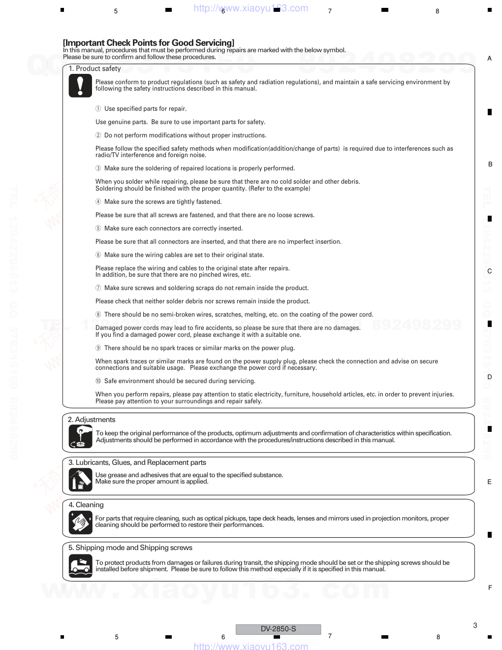
[Important Check Points for Good Servicing]
In this manual, procedures that must be performed during repairs are marked with the below symbol.
Please be sure to confirm and follow these procedures.
1. Product safety
Please conform to product regulations (such as safety and radiation regulations), and maintain a safe servicing environment by
following the safety instructions described in this manual.
1 Use specified parts for repair.
Use genuine parts. Be sure to use important parts for safety.
2 Do not perform modifications without proper instructions.
Please follow the specified safety methods when modification(addition/change of parts) is required due to interferences such as
radio/TV interference and foreign noise.
3 Make sure the soldering of repaired locations is properly performed.
When you solder while repairing, please be sure that there are no cold solder and other debris.
Soldering should be finished with the proper quantity. (Refer to the example)
4 Make sure the screws are tightly fastened.
Please be sure that all screws are fastened, and that there are no loose screws.
5 Make sure each connectors are correctly inserted.
Please be sure that all connectors are inserted, and that there are no imperfect insertion.
6 Make sure the wiring cables are set to their original state.
Please replace the wiring and cables to the original state after repairs.
In addition, be sure that there are no pinched wires, etc.
7 Make sure screws and soldering scraps do not remain inside the product.
Please check that neither solder debris nor screws remain inside the product.
8 There should be no semi-broken wires, scratches, melting, etc. on the coating of the power cord.
Damaged power cords may lead to fire accidents, so please be sure that there are no damages.
If you find a damaged power cord, please exchange it with a suitable one.
9 There should be no spark traces or similar marks on the power plug.
When spark traces or similar marks are found on the power supply plug, please check the connection and advise on secure
connections and suitable usage. Please exchange the power cord if necessary.
0 Safe environment should be secured during servicing.
When you perform repairs, please pay attention to static electricity, furniture, household articles, etc. in order to prevent injuries.
Please pay attention to your surroundings and repair safely.
2. Adjustments
To keep the original performance of the products, optimum adjustments and confirmation of characteristics within specification.
Adjustments should be performed in accordance with the procedures/instructions described in this manual.
4. Cleaning
For parts that require cleaning, such as optical pickups, tape deck heads, lenses and mirrors used in projection monitors, proper
cleaning should be performed to restore their performances.
3. Lubricants, Glues, and Replacement parts
Use grease and adhesives that are equal to the specified substance.
Make sure the proper amount is applied.
5. Shipping mode and Shipping screws
To protect products from damages or failures during transit, the shipping mode should be set or the shipping screws should be
installed before shipment. Please be sure to follow this method especially if it is specified in this manual.
www. xiaoyu163. com
QQ 376315150
9
9
2
8
9
4
2
9
8
TEL 13942296513
9
9
2
8
9
4
2
9
8
0
5
1
5
1
3
6
7
3
Q
Q
TEL 13942296513 QQ 376315150 892498299
TEL 13942296513 QQ 376315150 892498299
http://www.xiaoyu163.com
DV-2850-S
4
1
2
3
4
1
2
3
4
C
D
F
A
B
E
CONTENTS
SAFETY INFORMATION..................................................................................................................................... 2
1. SPECIFICATIONS ............................................................................................................................................ 5
2. EXPLODED VIEWS AND PARTS LIST ............................................................................................................ 6
2.1 PACKING SECTION .................................................................................................................................. 6
2.2 EXTERIOR SECTION............................................................................................................................... 8
2.3 05 DVD MECHA SECTION...................................................................................................................... 10
3. BLOCK DIAGRAM AND SCHEMATIC DIAGRAM.......................................................................................... 12
3.1 BLOCK DIAGRAM ................................................................................................................................... 12
3.2 OVERALL WIRING CONNECTION DIAGRAM........................................................................................ 14
3.3 DVD MT PCB (1/5) ASSY ........................................................................................................................ 16
3.4 DVD MT PCB (2/5) ASSY ........................................................................................................................ 18
3.5 DVD MT PCB (3/5) ASSY ........................................................................................................................ 20
3.6 DVD MT PCB (4/5) ASSY ........................................................................................................................ 22
3.7 DVD MT PCB (5/5) ASSY ........................................................................................................................ 24
3.8 OPERATION, OPERATION 2 and OPERATION 3 PCB ASSYS ............................................................. 26
3.9 POWER PCB (1/2) ASSY ........................................................................................................................ 28
3.10 POWER PCB (2/2) ASSY ...................................................................................................................... 30
3.11 WAVEFORMS ........................................................................................................................................ 32
4. PCB CONNECTION DIAGRAM ..................................................................................................................... 35
4.1 LOADING and SW PCB ASSYS.............................................................................................................. 35
4.2 DVD MT PCB ASSY................................................................................................................................. 36
4.3 OPERATION, OPERATION 2 and OPERATION 3 PCB ASSYS ............................................................. 40
4.4 POWER PCB ASSY................................................................................................................................. 44
5. PCB PARTS LIST ........................................................................................................................................... 46
6. ADJUSTMENT ............................................................................................................................................... 52
6.1 WHEN REPLACING DVD DECK ............................................................................................................. 52
6.2 TEST MODE ............................................................................................................................................ 53
6.3 DISC REMOVAL METHOD...................................................................................................................... 54
7. GENERAL INFORMATION............................................................................................................................. 55
7.1 DIAGNOSIS ............................................................................................................................................. 55
7.1.1 TEST MODE IN ................................................................................................................................. 55
7.1.2 DISPLAY SPECIFICATION OF THE TEST MODE............................................................................ 56
7.1.3 FUNCTIONAL SPECIFICATION OF THE SHORTCUT KEY ............................................................ 57
7.1.4 SPECIFICATION OF MODEL INFORMATION DISPLAY .................................................................. 58
7.1.5 FUNCTIONAL SPECIFICATION OF THE SERVICE MODE ............................................................. 59
7.1.6 METHOD FOR DIAGNOSING DEGRADATION OF THE LDS ON THE PICKUP ASSY .................. 60
7.1.7 TROUBLE SHOOTING...................................................................................................................... 61
7.2 DISASSEMBLY ........................................................................................................................................ 63
7.3 IC INFORMATION.................................................................................................................................... 68
7.4 DISC / CONTENT FORMAT PLAYBACK COMPATIBILITY ..................................................................... 78
8. PANEL FACILITIES ........................................................................................................................................ 80
8.1 FRONT PANEL SECTION ....................................................................................................................... 80
8.2 DISPLAY .................................................................................................................................................. 81
8.3 REMOTE CONTROL ............................................................................................................................... 82
www. xiaoyu163. com
QQ 376315150
9
9
2
8
9
4
2
9
8
TEL 13942296513
9
9
2
8
9
4
2
9
8
0
5
1
5
1
3
6
7
3
Q
Q
TEL 13942296513 QQ 376315150 892498299
TEL 13942296513 QQ 376315150 892498299
http://www.xiaoyu163.com
DV-2850-S
5
5
6
7
8
5
6
7
8
C
D
F
A
B
E
1. SPECIFICATIONS
Specifications
General
System . . . . . . . . . . . . . . . . . . . . . . DVD player
Power requirements . . AC 220–240 V, 50/60 Hz
Power consumption . . . . . . . . . . . . . . . . . 7 W
Power consumption (standby) . . . . . . 0.75 W
Weight . . . . . . . . . . . . . . . . . . . . . . . .
1.7 kg
Dimensions:
DV-2850 . . . 420 (W) x 49.5 (H) x 213.6 (D) mm
Operating temperature . . . . . . . +5°C to +35°C
Operating humidity . . . . . . . . . . . . . 5% to 85%
(no condensation)
AV connector output
AV Connector (21-pin connector assignment)
AV connector output . . . . . . . 21-pin connector
This connector provides the video and audio
signals for connection to a compatible colour TV
or monitor.
PIN no.
1. . . . . . . . . . . . . . . . . . . . . . . . Audio 2/R out
3. . . . . . . . . . . . . . . . . . . . . . . . . . Audio 1/L out
4. . . . . . . . . . . . . . . . . . . . . . . . . . . . . . . . GND
7. . . . . . . . . . . . . . . . . . . . . . . . . . . . . . . . B out
8. . . . . . . . . . . . . . . . . . . . . . . . . . . . . . Status
11. . . . . . . . . . . . . . . . . . . . . . . . . . . . . . . G out
15. . . . . . . . . . . . . . . . . . . . . . . . . . . . . . . R out
17. . . . . . . . . . . . . . . . . . . . . . . . . . . . . . . GND
19. . . . . . . . . . . . . . . . . . . . . . . . . . . Video out
21. . . . . . . . . . . . . . . . . . . . . . . . . . . . . . . GND
Component video output
Y (luminance) - Output level . . . 1 Vp-p (75 Ω )
PB (color) - Output level
PR (color) - Output level . . . . . 0.7 Vp-p (75 Ω)
Jack
S-video output
Y (luminance) - Output level . . .
1 Vp-p (75Ω )
C (color) - Output level. . . . .
286 mVp-p (75 Ω)
Jack . . . . . . . . . . . . . . . . . . . . . . . . . . . S-video
Video output
Output level . . . . . . . . . . . . . . .
1 Vp-p (75Ω)
Jack . . . . . . . . . . . . . . . . . . . . . . . . . . . . . . RCA
Audio output ( 1 stereo pair)
Output level . . . . . . . . . .
During audio output
200 mVrms (1 kHz, –20 dB)
Number of channels . . . . . . . . . . . . . . . . . . . 2
Jacks . . . . . . . . . . . . . . . . . . . . . . . . . . . . . RCA
Digital audio characteristics
Frequency response . . . . . . . . 4 Hz to 44 kHz
(DVD fs: 96 kHz)
S/N ratio . . . . . . . . . . . . . . . . . . . . . . . . .
115 dB
Dynamic range . . . . . . . . . . . . . . . . . . . .
101 dB
Total harmonic distortion . . . . . . . . . .
0.0023 %
Wow and flutter . . . . . . Limit of measurement
(±0.001% W. PEAK) or lower
Digital output
Coaxial digital output . . . . . . . . . . . . . RCA jack
Accessories
Audio/video cable. . . . . . . . . . . . . . . . . . . . . . . . 1
Power cable. . . . . . . . . . . . . . . . . . . . . . . . . . . . . 1
Remote control. . . . . . . . . . . . . . . . . . . . . . . . . . 1
AA/R6P dry cell batteries . . . . . . . . . . . . . . . . . 2
Warranty card. . . . . . . . . . . . . . . . . . . . . . . . . . . 1
Operating Instructions
The specifications and design of this product are subject to
change without notice, due to improvement.
Published by Pioneer Corporation.
Copyright © 2005 Pioneer Corporation.
All rights reserved
. . . . 0.7 Vp-p (75Ω )
. . . . . . . . . . . . . . . . . . . . . . . . . . . . . . RCA
www. xiaoyu163. com
QQ 376315150
9
9
2
8
9
4
2
9
8
TEL 13942296513
9
9
2
8
9
4
2
9
8
0
5
1
5
1
3
6
7
3
Q
Q
TEL 13942296513 QQ 376315150 892498299
TEL 13942296513 QQ 376315150 892498299
http://www.xiaoyu163.com
DV-2850-S
6
1
2
3
4
1
2
3
4
C
D
F
A
B
E
2. EXPLODED VIEWS AND PARTS LIST
2.1 PACKING SECTION
Parts marked by "NSP" are generally unavailable because they are not in our Master Spare Parts List.
The mark found on some component parts indicates the importance of the safety factor of the part.
Therefore, when replacing, be sure to use parts of identical designation.
Screws adjacent to mark on product are used for disassembly.
For the applying amount of lubricants or glue, follow the instructions in this manual.
(In the case of no amount instructions, apply as you think it appropriate.)
NOTES:
15
14
3
4
14
3
For WVXTL type
For WYXTL type
4
2
1
1
5
2
13
12
6
16
16
12
6
7
11
8-10
"Operating Instructions"
Front
www. xiaoyu163. com
QQ 376315150
9
9
2
8
9
4
2
9
8
TEL 13942296513
9
9
2
8
9
4
2
9
8
0
5
1
5
1
3
6
7
3
Q
Q
TEL 13942296513 QQ 376315150 892498299
TEL 13942296513 QQ 376315150 892498299
http://www.xiaoyu163.com
DV-2850-S
7
5
6
7
8
5
6
7
8
C
D
F
A
B
E
PACKING SECTION parts List
(2) CONTRAST TABLE
DV-2850-S/WVXTL and DV-2850-S/WYXTL are constructed the same except for the following :
Mark No.
Description
Part No.
>
1
Cord Set AC
See Contrast table (2)
2
Cord, RCA Pin
06CPBA2006
3
Remote Control
VXX2914
4
Battery Cover
VNK4998
NSP 5
Battery,Mangan (AR, R6P)
141L003010
NSP 6
Guarantee Card
J2G50202A
7
Operating Instructions(English) See Contrast table (2)
8
Operating Instructions
See Contrast table (2)
9
Operating Instructions
See Contrast table (2)
10
Operating Instructions
See Contrast table (2)
11
Package, Pad
792WHA0604
12
Polyethylene Bag
See Contrast table (2)
13
Gift Sheet
791WHA0108
14
Package
See Contrast table (2)
15
Gift Box
See Contrast table (2)
NSP 16
Poly. Bag
791WHAA040
Mark No.
Description
Part No.
Mark
No.
Symbol and Description
DV-2850-S/WVXTL
DV-2850-S/WYXTL
>
1
Cord Set AC
1206138802
1206158802
7
Operating Instructions (English)
J2G50101B
Not used
8
Operating Instructions (English, Italian)
Not used
J2G50321A
9
Operating Instructions (German, French)
Not used
J2G50322A
10
Operating Instructions (Spanish, Duch)
Not used
J2G50323A
12
Polyethylene Bag
JB5KD200
JB5K400
14
Package
792WHA0597
792WHA0588
15
Gift Box
793WCD1643
793WCDC717
www. xiaoyu163. com
QQ 376315150
9
9
2
8
9
4
2
9
8
TEL 13942296513
9
9
2
8
9
4
2
9
8
0
5
1
5
1
3
6
7
3
Q
Q
TEL 13942296513 QQ 376315150 892498299
TEL 13942296513 QQ 376315150 892498299
http://www.xiaoyu163.com
DV-2850-S
8
1
2
3
4
1
2
3
4
C
D
F
A
B
E
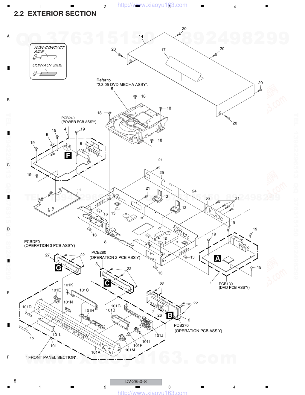
2.2 EXTERIOR SECTION
12
12
PCB130
(DVD PCB ASS'Y)
CONTACT SIDE
NON-CONTACT
SIDE
A
G
B
C
F
17
Refer to
"2.3 05 DVD MECHA ASSY".
" FRONT PANEL SECTION".
20
20
20
20
20
1
19
19
21
21
21
13
8
19
4
5
14
19
19
13
3
27
19
19
15
7
22
22
22
22
11
13
13
16
16
10
6
19
18
18
18
18
PCB240
(POWER PCB ASS'Y)
9
23
24
25
2
PCBDF0
(OPERATION 3 PCB ASS'Y)
PCB280
(OPERATION 2 PCB ASS'Y)
PCB270
(OPERATION PCB ASS'Y)
101
101A
101L
101D
101E
101M
101F
101I
101J
101K
101C
101H
101N
101G
101B
26
www. xiaoyu163. com
QQ 376315150
9
9
2
8
9
4
2
9
8
TEL 13942296513
9
9
2
8
9
4
2
9
8
0
5
1
5
1
3
6
7
3
Q
Q
TEL 13942296513 QQ 376315150 892498299
TEL 13942296513 QQ 376315150 892498299
http://www.xiaoyu163.com
DV-2850-S
9
5
6
7
8
5
6
7
8
C
D
F
A
B
E
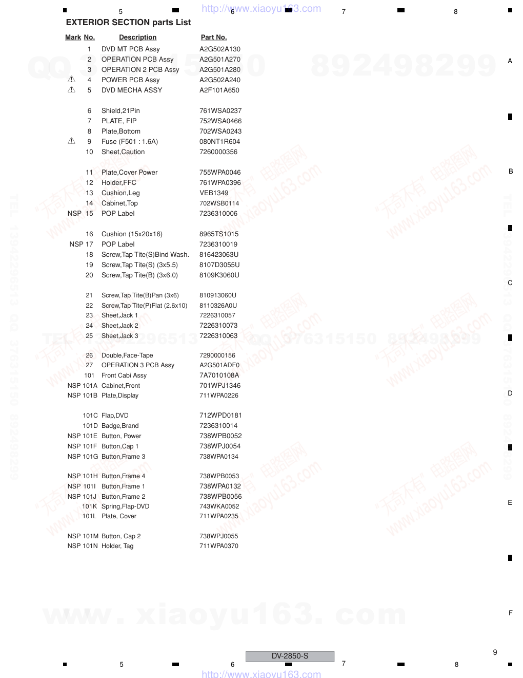
EXTERIOR SECTION parts List
Mark No.
Description
Part No.
1
DVD MT PCB Assy
A2G502A130
2
OPERATION PCB Assy
A2G501A270
3
OPERATION 2 PCB Assy
A2G501A280
>
4
POWER PCB Assy
A2G502A240
>
5
DVD MECHA ASSY
A2F101A650
6
Shield,21Pin
761WSA0237
7
PLATE, FIP
752WSA0466
8
Plate,Bottom
702WSA0243
>
9
Fuse (F501 : 1.6A)
080NT1R604
10
Sheet,Caution
7260000356
11
Plate,Cover Power
755WPA0046
12
Holder,FFC
761WPA0396
13
Cushion,Leg
VEB1349
14
Cabinet,Top
702WSB0114
NSP 15
POP Label
7236310006
16
Cushion (15x20x16)
8965TS1015
NSP 17
POP Label
7236310019
18
Screw,Tap Tite(S)Bind Wash.
816423063U
19
Screw,Tap Tite(S) (3x5.5)
8107D3055U
20
Screw,Tap Tite(B) (3x6.0)
8109K3060U
21
Screw,Tap Tite(B)Pan (3x6)
810913060U
22
Screw,Tap Tite(P)Flat (2.6x10)
8110326A0U
23
Sheet,Jack 1
7226310057
24
Sheet,Jack 2
7226310073
25
Sheet,Jack 3
7226310063
26
Double,Face-Tape
7290000156
27
OPERATION 3 PCB Assy
A2G501ADF0
101
Front Cabi Assy
7A7010108A
NSP 101A Cabinet,Front
701WPJ1346
NSP 101B Plate,Display
711WPA0226
101C Flap,DVD
712WPD0181
101D Badge,Brand
7236310014
NSP 101E Button, Power
738WPB0052
NSP 101F Button,Cap 1
738WPJ0054
NSP 101G Button,Frame 3
738WPA0134
NSP 101H Button,Frame 4
738WPB0053
NSP 101I
Button,Frame 1
738WPA0132
NSP 101J Button,Frame 2
738WPB0056
101K Spring,Flap-DVD
743WKA0052
101L Plate, Cover
711WPA0235
NSP 101M Button, Cap 2
738WPJ0055
NSP 101N Holder, Tag
711WPA0370
www. xiaoyu163. com
QQ 376315150
9
9
2
8
9
4
2
9
8
TEL 13942296513
9
9
2
8
9
4
2
9
8
0
5
1
5
1
3
6
7
3
Q
Q
TEL 13942296513 QQ 376315150 892498299
TEL 13942296513 QQ 376315150 892498299
http://www.xiaoyu163.com
DV-2850-S
10
1
2
3
4
1
2
3
4
C
D
F
A
B
E
2.3 05 DVD MECHA SECTION
Applying positions AA, AB and AC for the
grease are displayed for this section.
Check if the correct grease is applied for each
position.
NOTE:
CLASS
MARK
GREASE
G-478B
AA
PN-397
AB
PART NO.
GEM1018
PART NAME
GYA1001
ME-913A
AC
GEM1036
Cannot supply separately.
If the repair is needed, replace the
LOADER SUB ASS'Y.
PCB610
(LOADING MOTOR PCB ASS'Y)
CD2302
Do not replace the parts. Because,
minute adjustments are needed if
this condition is disassembled
further more.
If the repair is needed, replace the
DVD MECHA ASS'Y.
(SW PCB ASS'Y)
10
AB
AB
AB
AA
34
15
14
21
18
11
23
9
AB
19
1
29
AB
AB
3
12
20
6
4
SW1
31
PCB640
27
22
22
16
2
CD2001
24
5
25
26
32
8
13
35
8
30
SW2
33
CD2301
AC
AC
AB
D
E
Lubricating Oil
GYA1001
Daifree
GEM1036
Note :
Lubricating Oil
GYA1001
7
17
28
www. xiaoyu163. com
QQ 376315150
9
9
2
8
9
4
2
9
8
TEL 13942296513
9
9
2
8
9
4
2
9
8
0
5
1
5
1
3
6
7
3
Q
Q
TEL 13942296513 QQ 376315150 892498299
TEL 13942296513 QQ 376315150 892498299
http://www.xiaoyu163.com
DV-2850-S
11
5
6
7
8
5
6
7
8
C
D
F
A
B
E
05 DVD MECHA SECTION parts List
Mark No.
Description
Part No.
1
Loading Motor PCB Assy
A2F101A610
2
Gear,Middle
92P100117A
>
3
Loading Motor
1515S98004
4
Pulley,Motor
92P100097A
>
5
FEED Motor
1515S98004
6
Cord Jumper (24P)(CD2001)
122H0O2305
7
Cord Jumper (CD2302)
122H051602
8
Insulator (F)
92P200013A
9
Belt,Loading
92P200015A
10
Insulator (R)
92P200016A
11
Frame,main
92P100119A
12
Tray (B)
92P100127A
13
Holder ,Traverse
92P100125A
14
Gear,Pulley
92P100123A
15
Gear,Main
92P100124A
16
Gear,Feed
92P100116A
17
SW PCB Assy (PCB640)
A2F101A640
18
Plate,Clamper
92P000023A
19
Loader SUB Assy
92AAA0019A
20
Clamper
92P100122A
21
Screw,Pan (M1.7x3 P3)
814011730U
22
Screw,Pan (M1.7x2.3 P3)
814011723U
23
Rack,Loading
92P100121A
24
Gear,Motor
92P100088A
25
Feed Rack Assy
92AAA0017A
26
Screw,T-Tite(B) (M1.7x5.0 P3)
813381750U
27
Screw,Gear Feed
92P700007A
28
Cord Jumper (CD2301)
122H061605
29
Switch (SW1)
0515S32003
30
Push Switch (SW2)
0500101036
31
Screw,Tap Tite(P) (2.6x8)
811022680U
32
Sems.Tap Tite(P) (2x8)
816112080U
33
Screw (Bind 2x8)
811022080U
>
34
DVD MECHA ASSY
A2F101A650
NSP 35
Traverse SUB ASSY
92AAA0016A
www. xiaoyu163. com
QQ 376315150
9
9
2
8
9
4
2
9
8
TEL 13942296513
9
9
2
8
9
4
2
9
8
0
5
1
5
1
3
6
7
3
Q
Q
TEL 13942296513 QQ 376315150 892498299
TEL 13942296513 QQ 376315150 892498299
http://www.xiaoyu163.com
DV-2850-S
12
1
2
3
4
1
2
3
4
C
D
F
A
B
E
3. BLOCK DIAGRAM AND SCHEMATIC DIAGRAM
3.1 BLOCK DIAGRAM
11
11
A
CP2301
IC2301
Motor Drive
IC
X4001
(27MHz)
IC651
FIP Driver IC
V651 FL TUBE
IC4002
MPEG / MICON
/ RF-AMP
IC4004
16Mbit Flash
CP2303
CD2301
PICKUP
SPINDLE
MOTOR
10
10
B
7
7
C
S_Y
6
6
D
6
1
SP1+
5
2
SP1–
4
3
SLD+
3
4
SLD–
21
21
T+
22
22
T–
23
23
F+
24
24
F–
5
5
E
2
2
10
10
11
11
9
9
6
6
30
7
6
9
8
11
10
5
12
13
4
48
19
18
2
5
4
3
194
49
F
M
SLED
MOTOR
M
SW PCB ASSY
DVD MECHA
ASSY
D
DVD MT PCB ASSY
A
OPERATION 3
PCB ASSY
G
OPERATION 2
PCB ASSY
C
OPERATION
PCB ASSY
B
CP2302
CD2302
LOADING
MOTOR
SW1
2
4
LD+
1
5
LD–
3
3
OPEN
5
1
CLOSE
M
LOADING MOTOR
PCB ASSY
E
IC4005
64Mbit SDRAM
IC4001
EEPROM
S_C
196
R/CR
203
G/Y
200
B/CB
202
CVBS
198
228
229
ASPDIF
ASDAT0
CP4002
CP601
CP602
CP603
CP605
CP604
225
217
V+3E
V+3E
FLDC+
FLDC–
-28V
Power
www. xiaoyu163. com
QQ 376315150
9
9
2
8
9
4
2
9
8
TEL 13942296513
9
9
2
8
9
4
2
9
8
0
5
1
5
1
3
6
7
3
Q
Q
TEL 13942296513 QQ 376315150 892498299
TEL 13942296513 QQ 376315150 892498299
http://www.xiaoyu163.com
DV-2850-S
13
5
6
7
8
5
6
7
8
C
D
F
A
B
E
IC8002
Video Driver
6 ch
IC4006
REG+1.8V IC
IC8001
4 ch BUS SW
T501
Power Transformer
F501
Fuse
IC8004
Audio DAC
2 ch
IC8003
Audio LPF
& AMP
5
1
3
8
10
12
8
12
10
5
3
1
2
3
5
6
8
9
12
13
14
2
3
5
6
8
9
12
13
14
L
N
15
11
7
19
3
1
6
2
3
2
14
10
12
4
21
26
16
9
4
7
2
5
11
10
3
6
20
18
23
2
7
2
8
POWER PCB ASSY
F
V-OUT L
S_C OUT
R/CR out
S_Y OUT
L
J8003
J8002
J8004
R
Y
J8001
CP8001
CP503
CP502
CP4003
J8101
J501
CB
CR
CVBS
DIGITAL OUT
COAXIAL
AUDIO OUT
S VIDEO OUT
6
1
7
V-OUT R
VIDEO
OUT
R
L
CVBS
B
G
R
SCART
AC IN
G/Y out
B/CB out
R
G
B
CVBS
P.CON+12V
AUDIO L
AUDIO R
V out
AT+12V for MUTE
P.CON+5V
P.CON+6V
P.CON+3.3V
AT+3.3V
FL DC–
FL DC+
-28V
V+3
V+5V
V+5S
V+3A
V+3E
V+3F
V+12
V+12AT
V+6A
V+5A
(AUDIO DAC)
(MPEG SDRAM FLASH)
(AUDIO VIDEO DAC)
(FLIP/LED/IR/RESET)
(CORE)
(AUDIO AMP)
(AUDIO MUTE)
(MOTOR)
(VIDEO OPT/COAX)
(OPU)
(F/E)
V+1P8
www. xiaoyu163. com
QQ 376315150
9
9
2
8
9
4
2
9
8
TEL 13942296513
9
9
2
8
9
4
2
9
8
0
5
1
5
1
3
6
7
3
Q
Q
TEL 13942296513 QQ 376315150 892498299
TEL 13942296513 QQ 376315150 892498299
http://www.xiaoyu163.com
DV-2850-S
14
1
2
3
4
1
2
3
4
C
D
F
A
B
E
3.2 OVERALL WIRING CONNECTION DIAGRAM
24
23
22
21
20
19
2
1
18
17
16
15
14
13
12
11
10
9
8
7
6
5
4
3
24
23
22
21
20
19
2
1
18
17
16
15
14
13
12
11
10
9
8
7
6
5
4
3
24
23
22
21
20
19
2
1
18
17
16
15
14
13
12
11
10
9
8
7
6
5
4
3
CP2301
5
4
3
2
1
1
2
3
4
5
CP2302
6
5
4
3
2
1
CP2303
DVD/CD(SW)
LIMIT SW
LD-
LD+
GND(D)
CLOSE
OPEN
LOADING MOTOR
FG SENSER
SW(GND)
SLD-
SLD+
SP1-
SP1+
FFC
SLED MOTOR
SPINDLE
MOTOR
6
5
4
3
2
1
VREF
MON(DVD)
NC
VOL(DVD)
GND(DVD)
LD(DVD)
VOL(CD)
GND(CD)
GND(DVD)
MON(COM)
RF
C
B
A
D
F
E
VCC
GND
F-
F+
T-
T+
VS
NC
SW1(DVD/CD)
LD_DVD(650)
PD/GND
LD_CD(780)
VR780(CD)
GND
GND
VR650(DVD)
VRF(RF_OUT)
C
B
A
D
F
E
VCC
GND
TRKG RIN
TRKG DRV
FOCS RTN
FOCS DRV
1
2
3
4
5
6
OPTICAL PICKUP
SSS-13-2
SW1
GND(SW)
SW-2(CLOSE)
SW-1(OPEN)
LOADING MOTOR(-)
LOADING MOTOR(+)
BCZ3B52
M2603
GND(SW)
FEED MOTOR (+)
SPINDLE MOTOR (+)
SPINDLE MOTOR (-)
FEED MOTOR (-)
PICK UP INNER LIMIT SWITCH
JCV9B06
M2601
M
M
M
BCZ3B03
M2602
SW2
ESE22MH24
CD2301
CD2302
2H062102
2H052601
VRCOM
CP4002
11
10
9
8
7
6
5
4
3
2
1
11
10
9
8
7
6
5
4
3
2
1
CP601
CLK
DI (M to F)
STB
FL DC+
FL DC –
– 28V
DGND
DGND
V+ 3E
I R
DO (F to M)
3
4
5
6
7
CP602
CP605
CP604
7
6
5
4
3
CP603
069EVB3050
069EVB3030
069EV93050
069EV93050
069EV53050
069EV53050
7
6
5
4
3
3
8
2
4
5
6
7
2
V+3E
V+3E
PLAY/+SKIP
PLAY/+SKIP
SW2
PAUSE/–SKIP
POWER
8
GND
SW2
8
9
2
1
2
1
9
1
8
9
STOP
SW1
9
I R
5
4
3
5
4
3
PLAY/+SKIP
SW2
PAUSE/–SKIP
2
1
2
1
STOP
SW1
STOP
SW1
PAUSE/–SKIP
POWER
GND
1
IR
DVD MECHA ASSY (A2F101A650)
SW PCB ASSY
(A2F101A640)
D
LOADING MOTOR
PCB ASSY
(A2F101A610)
E
CD601(11P FFC)
122H0B1002
CD602(9P FFC)
122H092801
CD604(5P FFC)
122H051001
D E
OPERATION
PCB ASSY
(A2G501A270)
B
OPERATION 3
PCB ASSY
(A2G501ADF0)
G
OPERATION 2
PCB ASSY
(A2G501A280)
C
www. xiaoyu163. com
QQ 376315150
9
9
2
8
9
4
2
9
8
TEL 13942296513
9
9
2
8
9
4
2
9
8
0
5
1
5
1
3
6
7
3
Q
Q
TEL 13942296513 QQ 376315150 892498299
TEL 13942296513 QQ 376315150 892498299
http://www.xiaoyu163.com
DV-2850-S
15
5
6
7
8
5
6
7
8
C
D
F
A
B
E
CP502
14
13
12
11
10
9
8
7
6
4
5
3
2
1
CP4003
14
13
12
11
10
9
6
5
4
3
2
1
8
7
14
13
12
11
10
9
6
5
4
3
2
1
8
7
14
13
12
11
10
9
6
5
4
3
2
1
8
7
069J7C0599
069J7C0599
069S2E0629
AT+12V for MUTE
GND
P. CON+ 12V
GND
P. CON+5V
P. CON+6V
GND(M)
P. CON+3.3V
AT+3.3V
P. ON-H
GND(D)
FL DC –
FL DC +
– 28V
AT+12V for MUTE
GND
P. CON+ 12V
GND
P. CON+5V
P. CON+6V
GND(M)
P. CON+3.3V(AT)
AT+3.3V
STBY L
GND(D)
FL DC –
FL DC +
– 28V
CP503
12
11
10
9
8
7
6
4
5
3
2
1
CP8001
12
11
10
9
6
5
4
3
2
1
8
7
1
2
3
4
7
8
9
10
11
12
5
6
1
2
3
4
7
8
9
10
11
12
5
6
B/CB
G/Y
GND
GND
R/CR
RGB-H
FS
CVBS
GND
AUDIO L
GND
AUDIO R
B
G
GND
GND
R
RGB-H
FS
CVBS
GND
AUDIO L
GND
AUDIO R
÷ When ordering service parts, be sure to refer to "EXPLODED VIEWS and PARTS LIST" or
"PCB PARTS LIST".
÷ The > mark found on some component parts indicates the importance of the safety factor
of the part. Therefore, when replacing, be sure to use parts of identical designation.
÷
: The power supply is shown with the marked box.
DVD MT PCB ASSY (A2G502A130)
A 1/5- A 5/5
A
: MPEG/MICON/RF-AMP BLOCK
A 1/5
: MEMORY BLOCK
A 2/5
: LOADER/MOTOR DRV BLOCK
A 3/5
: AUDIO/VIDEO JACK BLOCK
A 4/5
: POWER PORT BLOCK
A 5/5
POWER PCB ASSY (A2G502A240)
F 1/2, F 2/2
F
: POWER BLOCK
F 1/2
: 21PIN/D/DIGITAL AUDIO BLOCK
F 2/2
CVBS
VIDEO OUT
(COMPOSITE)
J8001
J8002
Y
U
V
S VIDEO OUT
SCART
AUDIO OUT
DIGITAL OUT
L
J8003
R
COAXIAL
J8004
J8101
J501
LIVE
BLUE
BROWN
AC IN
1
2
NEUTRAL
Y
C
CD8001(12P FFC)
122HC0C3001
CP502(14P)
Cord Connector
06C32E3504
www. xiaoyu163. com
QQ 376315150
9
9
2
8
9
4
2
9
8
TEL 13942296513
9
9
2
8
9
4
2
9
8
0
5
1
5
1
3
6
7
3
Q
Q
TEL 13942296513 QQ 376315150 892498299
TEL 13942296513 QQ 376315150 892498299
http://www.xiaoyu163.com
DV-2850-S
16
1
2
3
4
1
2
3
4
C
D
F
A
B
E
3.3 DVD MT PCB (1/5) ASSY
A 1/5
R4020
15K
R4027
100
R4013
10K
R4014
10K
R4011
10K
R4012
10K
R4024
750K
R4025
100K
R4035
33
R4034
33
R4016
15K
R4017
22K
R4018
22K
R4019
22K
R4002
10K
R4026
10K
R4015
10K
R4003
680K
R4022
100K
R4001
1K
C4032
0.1
B
C4031
0.03
B
C4027
0.1
B
C4026
0. 1B
C4025
0. 1
B
C4030
0. 1 B
C4050 0 . 1B
C4019
0.1B
C4020
0.1B
C4013
0.1B
C4014
1B
C4015
1B
C4016
1B
C4042
0.047
B
B
C4044
0.047
C4021
0.1B
C4012
0.1B
C4001
0.0022B
C4002
270P
CH
C4022
0. 1
B
C4024 0 . 0015 B
C4043
0.1
B
C4048
10P CH
C4047
390P CH
C4049
11P CH
C4003
150P
CH
C4017
1B
C4080
1B
C4005
0.1B
C4008
0.1B
C4007
0.1B
C4009
0.015B
C4091
0.0022B
C4028
0.1
B
C4101
0.1
B
C4033
0. 001 B
C4102
0. 1 B
C4041
B
0.1
C4105
B
1
C4103
0. 1 B
C4104
1
B
C4035
0. 1 B
C4045
0 . 47 B
C4034
22P CH
C4046
1 0
25V
K A
C4023
220
6. 3V
Y K
W829
222
223
224
225
226
227
228
229
230
231
232
233
234
235
236
237
238
239
240
241
242
243
244
245
246
247
248
249
250
251
252
253
254
255
256
1
2
19
10
11
12
13
14
15
16
17
18
20
21
22
23
24
25
26
27
28
29
3
30
31
32
33
34
35
36
37
38
39
4
40
41
42
43
44
45
46
47
48
49
5
50
51
52
53
54
55
56
57
58
59
6
60
61
62
63
64
65 66 67 68 69 70 71 72 73 74 75 76 77 78 79 80 81 82 83 84 85 86 87 88 89 90 91 92 93 94 95 96 97 98 99
7
8
9
TP4015
TP4016
TP4017
TP4018
TP4019
TP4020
TP4021
TP4035
TP4012
TP4010
TP4011
TP4009
TP4007
TP4001
TP4002
TP4003
TP4004
TP4005
TP4006
TP4008
TP4036
TP4030
TP4031
TP4032
TP4022
TP4023
TP4024
TP4025
TP4026
TP4027
TP4028
TP4029
TP4033
TP4034
TP4096
TP4014
TP4013
TP4037
TP4107
5
6
7
8
1
2
3
4
X4001
100BT02701
27MHz
V+3
A{3}
V1P4
B{3}
C{3}
D{3}
E{3}
F { 3}
MDI1 { 3}
LDO1 { 3}
LDO2 { 3}
V1P4 { 3}
DMSO { 3}
FMSO { 3}
TRCLOSE { 3}
TROPEN { 3}
PWMOUT1 { 3}
TRSO { 3}
FOSO { 3}
TROUT { 3}
TRIN { 3}
STBY { 3}
V20 { 3}
LIMIT { 3}
D
IOA { 3}
A
DEICG { 3}
B
R F { 3}
O PO { 3}
C
O P+ { 3}
RF
O P- { 3}
D_GND { 2, 3, 4, 5}
E
F
MDI1
LDO2
LDO1
MA0 { 2}
MA1 { 2}
MA2 { 2}
V20
MA3 { 2}
V1P4
MA4 { 2}
MA5 { 2}
MA6 { 2}
MA7 { 2}
MA8 { 2}
MA9 { 2}
MA10 { 2}
OPO
MA11 { 2}
OP-
SDCKE{ 2}
SDCLK{ 2}
OP+
DBA0 { 2}
DMSO
DBA1 { 2}
FMSO
DCS#{ 2}
TROPEN
DRAS# { 2}
PWMOUT1
DCAS# { 2}
DWE#{ 2}
TRSO
DQM0{ 2}
FOSO
DQM1{ 2}
V1P4
DQ0 { 2}
DQ1 { 2}
DQ2 { 2}
DQ3 { 2}
DQ4 { 2}
DQ5 { 2}
TROUT
DQ6 { 2}
TRIN
DQ7 { 2}
DQ8 { 2}
STBY
DQ9 { 2}
TRCLOSE(ENDM)
DQ10{ 2}
DQ11{ 2}
A2
DQ12{ 2}
DQ13{ 2}
A3
DQ14{ 2}
A4
DQ15 { 2}
A5
A 0 { 2}
A6
A 1 { 2}
A 2 { 2}
A7
A 3 { 2}
A8
A 4 { 2}
A18
A 5 { 2}
A19
A 6 { 2}
A 7 { 2}
A 8 { 2}
SDA
A 9 { 2}
SCL
A10 { 2}
V+3
A11 { 2}
A12 { 2}
A13 { 2}
UWR#
URD#
A14 { 2}
A15 { 2}
A16 { 2}
A17 { 2}
A18 { 2}
A19 { 2}
A20 { 2}
AD0 { 2}
AD1 { 2}
AD2 { 2}
AD3 { 2}
AD4 { 2}
AD5 { 2}
AD6 { 2}
PWR#
A16
A15
A14
A13
A12
A11
A10
A20
PCE#
PRD#
AD0
AD1
AD2
AD3
AD4
AD5
AD6
AD7
A17
AD7 { 2}
A9
A1
A0
PWR# { 2}
PCE# { 2}
PRD# { 2}
FP_DI
FP_SCK
D_GND {2,3,4,5}
NC
NC
NC
NC
NC
NC
NC
FROM/TO MEMORY
NC
NC
AGND
DVDA
DVDB
DVDC
DVDRF[P
DVDRF[N
MA
MB
MC
DVDD
SB
SC
SD
CDFON
CDFOP
SVDD3
RFLV/RFON
SGND
V2REFO
V20
FEO
TEO
TEZIS[LV
DMO
FMO
PWMOUT1/V_ADIN9
FDO
USB_VDD3
TDI/V_ADIN4 (JTAG)
FG/V_ADIN8 (PU)
TCK/V_ADIN6 (JTAG)
TDO/V_ADIN7 (JTAG)
IOA2 (PU)
IOA3 (PU)
IOA4 (PU)
IOA5 (PU)
IDA7 (PU)
IOA6 (PU)
DVSS
APLLCAP
APLLVSS
IOA19 (PU)
IOA18 (PU)
HIGHA0 (PU)
DVDD18
65
66
67
68
254
253
255
256
APLLVSSVDD3
XIOWR
A16
HIGHA7 (PU)
DVDD3
HIGHA2 (PU)
HIGHA3 (PU)
HIGHA4 (PU)
HIGHA5 (PU)
HIGHA6 (PU)
HIGHA1 (PU)
IOA20
XIOCS (PU)
XIODE
DVDD3
AD0
AD1
AD2
AD3
DVSS (18)
AD4
AD5
AD6
IOA2/V_ADIN0
ALE (PU)
AD7
A17
I OA0 (PU)
DVSS (3)
XUWR (PU)
XURD (PU)
DVDD18
UP1_2 (PU)
UP1_3 (PU)
(PD) ASDATA4
MC_DATA (PD)
SPDIF
RFGND18
RFVDD18
XTALI
JITFO
JITFN
PLLVSS
IDACEXLP
PLLVDD3
LPFON
LPFIP
LPFIN
LPFOP
ADCVDD3
ADCVSS
RFVDD3
RFRPDC
RFRPAC
HRFZC
CRTPLP
RFGND
OSP
OSN
(3) DVSS
NC
NC
NC
NC
NC
TROPENPWM
USB_VSS
NC
NC
IOCA1 (PU)
CSO/RFOP
VREFO
TMS/V_ADIN5 (JTAG)
VCC
WP
SCL
SDA
NC
NC
NC
GND
3. 3V
1. 8V
TPI
MD
SA
AVDD3
IREF
RFGC
OP_OUT
OP_INN
OP_INP
FROM/TO LOADER/MOTOR DRV
MIDI1
TNI
MIDI2
LDO2
LDO1
TRO
XTALO
V+3RF
( V+3D)
ADIN
IOWR#
IOCE#
3/5
A
2/5
A
MMZ1608R102CT
POWER_ON
MPEG/MICON/RF-AMP
IC4002
MT1389FE/C2-L
EEPROM
IC4001
BR24L16FJ-WE2
DVD MT PCB ASSY (A2G502A130)
A 1/5
MPEG/MICON/RF-AMP BLOCK
ASPDIF
B4007
(RF)
(D)
(A)
(B)
(C)
(E)
(F)
(D)
(A)
(B)
(C)
(E)
(RF)
(RF)
(F)
(D)
1
17
www. xiaoyu163. com
QQ 376315150
9
9
2
8
9
4
2
9
8
TEL 13942296513
9
9
2
8
9
4
2
9
8
0
5
1
5
1
3
6
7
3
Q
Q
TEL 13942296513 QQ 376315150 892498299
TEL 13942296513 QQ 376315150 892498299
http://www.xiaoyu163.com
DV-2850-S
17
5
6
7
8
5
6
7
8
C
D
F
A
B
E
A 1/5
R4043
33
R4068
1 50 + - 1%
R4069
1 50 + - 1%
R4071
33
R4051
3 3
R4067
1 50 + - 1%
R4066
1 50 + - 1%
R4065
1 50 + - 1%
R4064
1 50 + - 1%
R4054 1 0K
R4052 1 0K
R4050 3 3
R4047 3 3
R4061
2. 7K+ - 1%
R40621 5K
R4036 33
R4070
33
R4046 1 0
R4084
1K
R4007
100
R4082
33
R4005
100
C4073
0. 1B
C4072
0. 1 B
C4067
0. 1
B
C4063
0. 1 B
C4061
0. 1 B
C4060 0 . 1 B
C4066
1
B
C4062
0. 1
B
C4064
0. 1
B
C4053
0. 1 B
C4054
220P
CH
C4068
0.1 B
C4074
0. 1 B
C4090
0. 0082
B
C4076
3 3P
CH
C4077 1 00P
CH
C4078
3 3P
CH
C4071
0.1 B
C4079 1 00P
CH
C4114
1
B
C4116
100P CH
C4110
100P CH
W816
W814
W813
W812
W811
W815
W832
W833
W834
100 101 102 103 104 105 106 107 108 109 110 111 112 113 114 115 116 117 118 119 120 121 122 123 124 125 126 127 128
129 130 131 132 133 134 135 136 137 138 139 140 141 142 143 144 145 146 147 148 149 150 151 152 153 154 155 156 157 158 159 160 161 162 163 164 165 166 167 168 169 170 171 172 173 174 175 176 177 178 179 180 181 182 183 184 185 186 187 188 189 190 191 192
193
194
195
196
197
198
199
200
201
202
203
204
205
206
207
208
209
210
211
212
213
214
215
216
217
218
219
220
221
TP4044
TP4051
TP4052
TP4053
TP4054
TP4055
TP4056
TP4057
TP4058
TP4059
TP4063
TP4062
TP4061
TP4067
TP4068
TP4066
TP4060
TP4045
P4048T
TP4095
TP4065
TP4064
P4043T
TP4041
TP4039
TP4038
TP4050
TP4049
TP4047
TP4046
TP4103
TP4040
TP4097
TP4105
TP4104
TP4100
TP4101
TP4102
TP4076
TP4077
TP4078
TP4079
TP4080
TP4081
TP4082
TP4086
TP4087
TP4088
TP4085
TP4084
TP4083
TP4070
TP4071
TP4072
TP4075
TP4069
TP4073
TP4074
TP4093
TP4099
TP4098
TP4042
TP4106
TP4094
TP4108
TP4092
TP4091
TP4089
TP4090
IC4003
BD5229G-TR
1
4
5
2
3
1
10
11
2
3
4
5
6
7
8
9
NR4002
4D03WGJ0330T5E
NR4001
4D03WGJ0330T5E
SCK
SD
S_C
S_Y
IOA
R/CR
B/CB
G/Y
V+3A
CVBS
ACLK
ABCK
DEICG
XAMUTE
ASDAT0
ALRCK
DAC_XCS0
VSEL1 {4}
LETTER {4}
SQUEEZE {4}
I/XP{4}
R/CR {4}
B/CB {4}
G/Y {4}
CVBS {4}
V+3V
S_C { 4}
S_Y { 4}
SD{4}
SCK {4}
DAC_XCS0 {4}
XAMUTE {4}
ALRCK {4}
ABCK {4}
ACLK {4}
ASDAT0 {4}
ASPDIF {4}
D_GND{2,3,4,5}
VSEL1
VSEL2
LETTER
SQUEEZE
POWER_ON {5}
V+1R8 {5}
V+3 {2,5}
V+3E {5}
V+3A {4,5}
I/XP
FLDC- {5}
FLDC+ {5}
-28V {5}
D_GND {2,3,4,5}
MA4
MA5
MA6
MA7
MA8
MA9
MA11
SDCKE
SDCLK
MA3
MA2
MA1
MA0
MA10
V+3(V+3D)
DBA1
RXD
DBA0
TXD
D_GND
DCS#
DRAS#
DCAS#
DWE#
DQM1
DQ8
FP_SCK
FP_DI
DQ9
STB
DQ10
FP_DO
DQ11
DQ12
IR
DQ13
V+3E
URST#
FLDC+
- 28V
V+3E
FLDC-
DQM0
DQ15
DQ14
DQ7
DQ6
DQ5
DQ4
DQ3
DQ2
DQ1
DQ0
FP_DO
LIMIT
URST#
V+3
V+1R8
STB
SCL
SDA
RXD
TXD
I R
NC
NCNC
NC
NC
NC
NC
NC
NC
NC
NC
NC
NC
NC
NC
NC
NC
UP1_4 (PU)
UP1_5 (PU)
UP1_6 (PU)
UP1_7 (PU)
UP3_0 (PU)
UP3_1 (PU)
UP3_4 (PU)
PU3_5 (PU)
DVDD3
ICE (PD)
XPRST (PU)
I R
XINT0 (PU)
DQM0
DQS0
RD7
DVSS (18)
RD6
125
126
127
128
RD5
DVSS (3)
RD4
RD3
DVDD18
RD2
RD1
RD0
RD15
DVDD3
RD14
RD13
RD12
RD11
RD10
RD9
(3) DVSS
DQS1
RD8
DQM1
XCAS
DVDD3
XRCS
BA0
(18) DVSS
BA1
RA10
RA0
(3) DVSS
RA1
RA2
RA3
DVDD18
DVDD3
RCLK
RA11
RA9
RA8
(3)DVSS
RA7
(18) DVSS
RA6
RA5
RA4
(PU) RD3/ASDATA5
(PU) RD30
RD29
DVDD18
RD26
RD25
RD24
(PD) DQM3
(PD) DQM2
DVDD3
DACVDDC
VREF
FS
192
191
190
189
DVDD3
VSYN/V_ADIN1
YUT7/ASDATA5
SPMCLK
SPDATA
SPLRCK
SPBCK/ADTA5
(PD) ALRCK
ABCK
ACLK
(18) DVSS
(PD) ASDATA1
(PD) ASDATA2
(PD) ASDATA3
(PD) ASDATA0
DVDD18
NC
NC
NC
NC
NC
NC
NC
NC
NC
NC
NC
NC
NC
YUV1/Y
YUV5/B
YUV0/CIN
DVDD3
HSYN/V_ADIN2
FROM/TOVIDEO/AUDIO
FROM/TOPOWER PORT
VSS
V_OUT
VDD
CT
NC
NC
DI (Mto F)
DO(F to M)
V+3E
FLDC+
-28V
FLDC-
I R
STB
CLK
DGND
DGND
XRWE
CKE
DVDD3
YUV6/R
DACVSSA
YUV4/G
DACVDDA
YUV3/CVBS
DACVSSB
YUV2/C
DACVDDB
DACVSSC
RXD
TXD
GND
V+3D
PP DEL
V+3D
1. 8V
CP4002
00_6232_011_006_800+
4/5
A
5/5
A
CP601
B
3.3V
RESET IC
XRAS
: VIDEO SIGNAL ROUTE
(RF)
: RF SIGNAL ROUTE
(SY)
: S VIDEO SIGNAL ROUTE (Y ch)
(SC)
: S VIDEO SIGNAL ROUTE (C ch)
(R/CR)
: VIDEO SIGNAL ROUTE (R/CR ch)
(G/Y)
: VIDEO SIGNAL ROUTE (G/Y ch)
(B/CB)
: VIDEO SIGNAL ROUTE (B/CB ch)
(D)
: AUDIO DATA SIGNAL ROUTE
(DA)
: AUDIO SIGNAL ROUTE (Digital)
(SY)
(SC)
(SY)
(SC)
(R/CR)
(G/Y)
(B/CB)
(R/CR)
(G/Y)
(B/CB)
(DA)
(D)
(DA)
www. xiaoyu163. com
QQ 376315150
9
9
2
8
9
4
2
9
8
TEL 13942296513
9
9
2
8
9
4
2
9
8
0
5
1
5
1
3
6
7
3
Q
Q
TEL 13942296513 QQ 376315150 892498299
TEL 13942296513 QQ 376315150 892498299
http://www.xiaoyu163.com
DV-2850-S
18
1
2
3
4
1
2
3
4
C
D
F
A
B
E
3.4 DVD MT PCB (2/5) ASSY
C4081
0. 001 B
A17
DQ0 { 1}
DQ1 { 1}
DQ 2 { 1}
DQ 3 { 1}
DQ 4 { 1}
DQ 5 { 1}
DQ 6 { 1}
DQ 7 { 1}
A0
DQ 8 { 1}
DQ 9 { 1}
DQ10 { 1}
AD7
DQ11 { 1}
DQ12 { 1}
DQ13 { 1}
DQ14 { 1}
DQ15 { 1}
M A0 { 1}
AD6
M A1 { 1}
M A2 { 1}
M A3 { 1}
M A4 { 1}
M A5 { 1}
M A6 { 1}
AD5
M A7 { 1}
M A8 { 1}
M A9 { 1}
MA10 { 1}
MA11 { 1}
DWE# { 1}
AD4
SDCKE { 1}
SDCLK { 1}
DQM1 { 1}
DQM0 { 1}
DCAS# { 1}
DRAS# { 1}
DBA1 { 1}
DBA0 { 1}
DCS# { 1}
AD3
A0 { 1}
A1 { 1}
AD2
A2 { 1}
A3 { 1}
A4 { 1}
A5 { 1}
A6 { 1}
A7 { 1}
AD1
A8 { 1}
A9 { 1}
A10 { 1}
A11 { 1}
A12 { 1}
A13 { 1}
AD0
A14 { 1}
A15 { 1}
A16 { 1}
PRD#
A17 { 1}
A18 { 1}
A19 { 1}
A20 { 1}
AD0 { 1}
AD1 { 1}
PCE#
AD2 { 1}
AD3 { 1}
AD4 { 1}
A1
AD5 { 1}
AD6 { 1}
AD7 { 1}
PRD# { 1}
PCE# { 1}
PWR# { 1}
V+3 { 1, 5}
D_GND {1,3,4,5}
FROM/TOMPEG/MICON/DSP
(V+3D)
A 2/5
1/5
A
1/5
A
DVD MT PCB ASSY (A2G502A130)
A 2/5
MEMORY BLOCK
www. xiaoyu163. com
QQ 376315150
9
9
2
8
9
4
2
9
8
TEL 13942296513
9
9
2
8
9
4
2
9
8
0
5
1
5
1
3
6
7
3
Q
Q
TEL 13942296513 QQ 376315150 892498299
TEL 13942296513 QQ 376315150 892498299
http://www.xiaoyu163.com
DV-2850-S
19
5
6
7
8
5
6
7
8
C
D
F
A
B
E
1
10
11
12
13
14
15
16
17
18
19
2
20
21
22
23
24
25
26
27
28
29
30
31
32
33
34
35
36
37
38
39
40
41
42
43
44
45
46
47
48
49
50
51
52
53
54
48
47
46
45
44
43
42
41
40
39
38
37
36
35
34
33
32
31
30
29
28
27
26
25
3
4
5
6
7
8
9
1
10
11
12
13
14
15
16
17
18
19
2
20
21
22
23
24
3
4
5
6
7
8
9
R4087
10K
C4082
0. 1 B
C4088
0. 1B
C4085
0.1
B
C4084
0.1
B
C4086
1000
6. 3V
Y K
W820
DQ15
A16
A15
DQ14
DQ6
A14
DQ13
DQ5
A13
A12
DQ12
DQ4
A11
DQ11
DQ3
A10
A9
DQ10
DQ2
A20
DQ9
DQ1
PWR#
DQ8
DQ0
DQM0
DQM1
DWE#
SDCLK
DCAS#
A19
SDCKE
DRAS#
A18
DCS#
A8
MA11
DBA0
A7
MA9
DBA1
A6
MA8
MA10
A5
MA7
MA0
A4
MA6
MA1
A3
MA5
MA2
A2
MA4
MA3
0
0
1. 4
2. 6
2. 6
1. 4
1. 2
1. 6
1. 6
3. 3
1. 3
0. 9
1. 6
2. 5
1. 5
1. 6
1. 3
2. 5
1. 5
0. 8
1. 0
1. 7
0
0. 1
0
0
3. 3
1. 6
0. 8
0
0. 7
0. 6
1. 2
1. 3
1. 9
0. 7
1. 2
3. 3
A16
VSS
VSS
A0
A7
A6
A5
A4
A3
A2
A1
A15
A14
A13
A12
A11
A9
A8
A18
A17
A10
A19
0. 1
1. 6
0. 7
1. 4
1. 6
1. 3
1. 6
1. 7
2. 5
1. 6
D15
D7
D14
D6
D13
D5
D12
D4
VCC
D11
D3
D10
D2
D9
D1
D8
D0
NC
NC
NC
NC
NC
NC
NC
NC
NC
NC
NC
NC
NC
NC
NC
NC
VCC
VSS
DQ0
DQ1
DQ2
DQ15
VSSQ
DQ13
VQ14
DQ12
DQ11
VSSQ
DQ3
DQ4
VDDQ
DQ5
DQ6
VSSQ
DQ7
VSSQ
DQ10
DQ9
DQ8
VCC
LDQM
VSS
UDQM
NC
A9
A11
A10/AP
A0
A2
A1
A3
VSS
A4
A5
A6
A7
A8
BA0
BA1
VCCQ
CKE
CLK
NC
VCC
CS
ASR
ASC
WE
VCCQ
VCCQ
OE#
CE#
RY/BY#
RESET#
WE#
BYTE#
A 2/5
16Mbit FLASH
IC4004 S29AL016D
64Mbit SDRAM
IC4005 K4S641632H-UC75
DQ7
www. xiaoyu163. com
QQ 376315150
9
9
2
8
9
4
2
9
8
TEL 13942296513
9
9
2
8
9
4
2
9
8
0
5
1
5
1
3
6
7
3
Q
Q
TEL 13942296513 QQ 376315150 892498299
TEL 13942296513 QQ 376315150 892498299
http://www.xiaoyu163.com
DV-2850-S
20
1
2
3
4
1
2
3
4
C
D
F
A
B
E
3.5 DVD MT PCB (3/5) ASSY
Q2301
KTC3875S_Y_RTK
1
10
11
12
13
14
15
16
17
18
19
2
20
21
22
23
24
3
4
5
6
7
8
9
1
2
3
4
5
1
2
3
4
5
6
S
D
G
Q2306
2SK3018T106
S
D
G
Q2307
2SK3018T106
R2308
10K
R2307
100K
R2309
10K
R2306
100K
R2338
10K
2329R
1
R2342
680K
R2319
150K
R2331
150K
C2303
0 . 1B
C2301
0 . 1 B
C2302
0 . 1 B
C2314
1 B
C2322
0. 0022 B
C2323
0. 1 B
C2325
0. 001 B
TP2303
TP2305
TP2306
TP2309
TP2310
TP2311
TP2312
TP2313
TP2314
TP2315
TP2316
TP2317
TP2318
TP2319
TP2308
TP2307
TP2320
TP2321
TP2322
TP2323
TP2301
TP2302
TP2304
JG002
JG003
JG004
JG005
JG006
JG007
JG001
TP2327
TP2328
TP2326
TP2325
TP2324
TP2331
IOA
V+5S
DEICG
V+5S
F
V20
E
D
C
IOA
RF
B
A
MDI1
T+
T-
F+
F-
LOAD-
LOAD+
TROUT
V+6A
TRIN
OPO
OP-
OP+
LIMIT
MOT_SLED-
MOT_SLED+
MOT_SPDL+
MOT_SPDL-
V+3F
FG
LOAD+
LOAD-
GND
OPEN
CLOSE
VRCOM
TRKG DRV
TRKGRTN
FOCS RTN
FOCS DRV
VCC
D
B
VR780(CD)
VRF(RF_OUT)
SW1(DVD/CD)
C
E
VS
F
GND
A
VR650(DVD)
GND
GND
LD_DVD(650)
LD_CD(780)
PD/GND
NC
NC
SW(GND)
LIMIT SW
SLD-
SLD+
SPD-
SPD+
CP2303
00_6232_006_006_800+
CP2302
00_6232_005_006_800+
CP2301
09-5000-024-001-001
CD2302
To PICKUP
E
CD2301
D
A 3/5
DVD MT PCB ASSY (A2G502A130)
A 3/5
LOADER/MOTOR DRV BLOCK
(F)
(F)
(E)
(E)
(D)
(D)
(C)
(C)
(B)
(B)
(RF)
(RF)
(A)
(A)
www. xiaoyu163. com
QQ 376315150
9
9
2
8
9
4
2
9
8
TEL 13942296513
9
9
2
8
9
4
2
9
8
0
5
1
5
1
3
6
7
3
Q
Q
TEL 13942296513 QQ 376315150 892498299
TEL 13942296513 QQ 376315150 892498299
http://www.xiaoyu163.com
DV-2850-S
21
5
6
7
8
5
6
7
8
C
D
F
A
B
E
Q2304
KTA1504S_Y_RTK
D DRIV for CDL
Q2305
KTA1504S_Y_RTK
LD DRIV for DVD
Q2302
KTA1504S_Y_RTK
LD DRIV for CD
Q2303
KTA1504S_Y_RTK
LD DRIV for DVD
IC2301
LA6565
19
1
2
3
4
5
6
7
8
9
10
11
12
13
14
15
16
17
18
20
21
22
23
24
25
26
27
28
29
30
31
32
33
34
35
36
37
38
R2317
56K + - 1%
R2312
15K + - 1%
R2311
10K
R2318
10 K
+ - 1%
R2326
4. 7K
R2327
4. 7K
R2330
10K + - 1%
R2328
10K
+ - 1%
R2316
10K + - 1%
R2313
10K + - 1%
R2325
15K + - 1%
R2335
2. 2
R2334
2. 2
R2332
1. 2
R2333
1. 2
R2320
4. 7
R2321
4. 7
R2323
4. 7
R2310
2. 7K
R2337
5. 6K
R2322
4. 7
C2307
1 B
C2312
1 B
C2313
0. 01B
C2311
0. 01B
C2310
0. 01B
C2308
0. 1
B
C2309
0. 1
B
C2305
0. 1 B
C2320
100
10V
Y K
C2321
100
10V
Y K
C2306
1 00
10V
Y K
W817
W809
W819
TP2333
TP2334
TP2329
TP2330
TP2339
TP2340
TP2341
TP2342
TP2332
JG009
JG008
JG010
TP2336
TP2335
TP2338
TP2337
RF {1}
DEICG {1}
V20 {1}
A { 1}
B { 1}
C { 1}
D { 1}
E { 1}
V+3F
F { 1}
MDI1 {1}
LDO2 {1}
LDO1 {1}
IOA {1}
LDO1
V1P4 {1}
LIMIT {1}
TROUT {1}
TRIN {1}
STBY {1}
DMSO {1}
Fv
TRCLOSE {1}
TROPEN {1}
PWMOUT1 {1}
TRSO {1}
LDO2
FOSO {1}
OPO {1}
Ov
OP- {1}
V+3F { 5}
V+5S { 5}
TRSO
FOSO
V+9A
D_GND {1,2,4,5}
M_GND {5}
STBY
DMSO
V1P4
PWMOUT1
FMSO
TRCLOSE
TROPEN
LOAD-
LOAD+
MOT_SPDL-
MOT_SPDL+
MOT_SLED-
MOT_SLED+
T-
T+
F-
F+
S-GND
VCONT
VIN4-
VREF-IN
VIN3
VCC1
VD2-
VD2+
VD3-
VD3+
VD4-
VD4+
VLD+
VCC2
VLD-
REV
FWD
VD1-
VD1+
VIN1+A
VIN1-A
VIN 1
VIN2+
VIN2-
VIN2
VIN3-
VO_OP
VIN-OP
VIN+OP
REG-IN
REG-OUT
VREF-OUT
MUTE234
MUTE1
VCCS
VIN4
TRACK
SPINDLE
FOCUS
DVD
RF33
FROM/TO POWER PORT
SLED
FROM/TO MPEG/MICON/RF-AMP
CD
3. 3
3. 3
3. 3
0
0
3. 3
2.0
3.1
3.1
2.0
2.5
2.5
NC
NC
NC
NC
NC
NC
0
3. 3
3. 3
1. 4
1. 4
1. 4
1. 4
0
0
0. 9
1. 6
1. 6
5. 9
1. 4
1. 4
1. 1
1. 4
1. 4
4. 1
5. 9
5. 9
0
0
0. 1
0
2. 6
2. 6
2. 6
2. 6
0
1. 5
3. 7
2. 6
2. 6
5. 9
1. 4
1. 4
1. 4
1/5
A
5/5
A
MOTOR DRIVE IC
A 3/5
(RF)
: RF SIGNAL ROUTE
(A)
(RF)
(B)
(C)
(D)
(E)
(F)
17
18
15
16
www. xiaoyu163. com
QQ 376315150
9
9
2
8
9
4
2
9
8
TEL 13942296513
9
9
2
8
9
4
2
9
8
0
5
1
5
1
3
6
7
3
Q
Q
TEL 13942296513 QQ 376315150 892498299
TEL 13942296513 QQ 376315150 892498299
http://www.xiaoyu163.com
DV-2850-S
22
1
2
3
4
1
2
3
4
C
D
F
A
B
E
3.6 DVD MT PCB (4/5) ASSY
n
G
1
2
3
4
5
6
7
8
9
10
11
12
13
14
15
16
1
10
11
12
13
14
15
16
17
18
19
20
2
3
4
5
6
7
8
9
H1
H2
E
H1
H2
E
1
2
3
4
5
6
CAUTION: DIGITAL TRANSISTOR
CAUTION: DIGITAL TRANSISTOR
1
10
11
12
2
3
4
5
6
7
8
9
CD8001
2H0C3001
R8027
75 + - 1%
R8029
75 + - 1%
R8028
75 + - 1%
R8024
75 + - 1%
R8016
1. 2K
R8017
1.2K
R8018
1.2K
C8001
0. 1B
C8003
1 B
C8006
1 B
C8002
1 B
C8004
0. 1B
C8008
0. 1
B
C8015
0. 1 B
C8016
0. 1 B
C8005
0. 1 B
C8010
0. 1 B
C8014
100
10V
Y K
C8017
100
10V
Y K
C8024
470
6. 3V
Y K
C8022
1000
6. 3V
Y K
C8023
470
6. 3V
Y K
C8026
1000
6. 3V
Y K
B8001
MMZ1608R102CT
B8002
MMZ1608R102CT
B8007
MMZ1608R102CT
B8006
MMZ1608R102CT
VSEL1
SQUEEZE
AUDIO_R
AUDIO_L
P-H/I-L_RGB-H
G/Y_OUT
DAC_XCS0 {1}
LETTER {1}
B/U_OUT
SQUEEZE {1}
XAMUTE {1}
ACLK {1}
R/V_OUT
ASPDIF {1}
SCK {1}
SD {1}
VSEL1 {1}
I/XP {1}
ABCK{1}
ASDAT0{1}
ALRCK{1}
R/CR{1}
B/CB{1}
G/Y {1}
CVBS {1}
S_C {1}
S_Y {1}
D_GND {1,2,3,5}
V+12AT {5}
V+12 {5}
V+5V {5}
V+5A {5}
V+3A {1,5}
ASP/FS
S_C_OUT
S_Y_OUT
CVBS_OUT
LETTER
SQUEEZE
V+5V
S_C
CB_OUT
CR_OUT
Y_OUT
CVBS
S_Y
VSEL1
G/Y
B/CB
R/CR
I/XP
P-H/I-L_RGB-H
VSEL1
FROM/TO POWER
R/CR
G/Y
B/CB
GND
GND
RGB-H
FS
AUDIO L
GND
AUDIO R
CVBS
GND
FROM/TO MPEG/MICON/DSP
NC
NC
NC
IN
GND
DB
S2B
S1B
DA
S2A
S1A
VCC
DC
S2C
S1C
DD
S2D
/EN
S1D
V in
YC MIX
Y in
I / P
CY in
CLP
Vcc2
C uot
S1
S2
GND2
Y out
CY out
GND2
Cb out
Cr out
GND2
Cr in
MUTE2
Cb i
ND2
V out
GND1
BIAS
DC out
Y
CB
CR
CVBS
C in
MUTE1
Vcc1
5.1
2.5
1.8
1.8
0
2.5
1.8
3.3
0
2.5
5.1
2.5
5.1
5.1
2.5
2.6
2.6
2.6
2.5
2.5
0
0
0
0
0
0
0
5.1
YUV/RGB both ---> IC8001 MOUNT,JP DEL
YUV only ---> W810,W821,W822 ON
RGB only ---> W863,W864,W865 ON
1/5
A
5/5
A
CP8001
IMSA-9604S-12C
VIDEO DRIVER 6CH
IC8002
MM1623BFBE
21
22
23
24
25
26
27
28
4CH BUS SW
IC8001
SN74CBT3257PWR
A 4/5
DVD MT PCB ASSY (A2G502A130)
A 4/5
AUDIO/VIDEO JACK BLOCK
J8001
MSP-244V10-95_NI_FE_LF
CVBS/Y/U/V
CP503
F 1/2
: VIDEO SIGNAL ROUTE
(SY)
(SY)
(SC)
: S VIDEO SIGNAL ROUTE (Y ch)
(SC)
: S VIDEO SIGNAL ROUTE (C ch)
(SY)
(SC)
(R/CR)
(R/CR)
: VIDEO SIGNAL ROUTE (R/CR ch)
(G/Y)
(G/Y)
: VIDEO SIGNAL ROUTE (G/Y ch)
(B/CB)
(B/CB)
: VIDEO SIGNAL ROUTE (B/CB ch)
(R)
(G)
(B)
(R)
(G)
(B)
(R)
(CR)
(G)
(B)
(R/CR)
(R/CR)
(R/CR)
(G/Y)
(G/Y)
(G/Y)
(B/CB)
(B/CB)
(B/CB)
(D)
(D)
: AUDIO DATA SIGNAL ROUTE
(DA)
(DA)
: AUDIO SIGNAL ROUTE (Digital)
: AUDIO SIGNAL ROUTE (L ch)
(SC)
(SY)
(SC)
(Y)
(CB)
(SY)
12
10
11
9
14
13
www. xiaoyu163. com
QQ 376315150
9
9
2
8
9
4
2
9
8
TEL 13942296513
9
9
2
8
9
4
2
9
8
0
5
1
5
1
3
6
7
3
Q
Q
TEL 13942296513 QQ 376315150 892498299
TEL 13942296513 QQ 376315150 892498299
http://www.xiaoyu163.com
DV-2850-S
23
5
6
7
8
5
6
7
8
C
D
F
A
B
E
Q8013
DTC114YUA
MUTE CTL
Q8010
DTC114YUA
MUTE CTL
1
2
3
4
5
6
7
8
9
10
11
12
13
14
15
16
1
2
3
4
5
6
D8007
1SS355
D8005
UDZS6.8B
H
E
COAXIAL
1
2
H1
H2
E
1
2
3
Q8005
KTC3875S_Y_RTK
COAXIAL DRIV
Q8019
2SD2114K
MUTE SW
Q8018
2SD2114K
MUTE SW
Q8021
2SD2114K
MUTE SW
Q8020
2SD2114K
MUTE SW
Q8016
KTC3875S_Y_RTK
REF VOL GEN
Q8014
KTA1504S_Y_RTK
JACK MUTE CTL
R8056
4. 7K
R8074
22K
R8073
22K
R8079
220
+ - 1%
R8078
470
R8081
470
R8084
220 + - 1%
R8046
2. 2K
R8038
220
R8036
3. 9K
R8037
1. 8K
R8035
2.2K
R8039
68
R8040
100K
R8044
10K
R8067
18K
+-1%
R8066
10K
+- 1%
R8083
470
R8080
220 + - 1%
R8085
220 + - 1%
R8060
270K
R8059
10K + - 1%
R8049
10K + - 1%
R8048
270K
R8076
470
R8061
10K + - 1%
R8063
1 8K + - 1%
R8077
220
+ - 1%
R8082 2 20 + - 1%
R8023
75 + - 1%
R8026
75 + - 1%
R8021
10K
R8065
10
R8070
33
R8051
3.9K
R8014
3.9K
R8069
680K
R8057
100
R8054
2. 2K
C8042
100PCH
C8074
330P
CH
C8068
0. 1 B
C8078
330P CH
C8077
330P CH
C8075
0.1 B
C8069
100P CH
C8058
0. 1 B
C8059
0. 1 B
C8057
560P CH
C8056
560P CH
C8067
100PCH
C8021
0. 1 B
C8036
1
B
C8063
0. 1 B
C8072
0. 1 B
C8046
C100PH
C8062
1 B
C8076
100
10V
Y K
C8038
1
50V
K A
C8073
47
16V
Y K
C8053
100
10V
Y K
C8051
100
10V
Y K
C8070
47
16V
Y K
C8025
470
6. 3V
Y K
C8066
100
10V
Y K
C8061
1000
6. 3V
Y K
W824
W866
1
2
3
4
5
6
7
8
B8004
MMZ1608R102CT
B8003
MMZ1608R102CT
SD
SCK
V+12AT
V+5A
V+3A
ALRCK
ABCK
ACLK
V+5V
ASPDIF
XAMUTE
ASDAT0
DAC_XCS0
AUDIO_L
GND
AUDIO_R
VSEL1
V+12
5V
GND
MC
MD
BCKIN
ZERO L
ZERO R
AGND
L
R
+
-
-
+
+VS
-VS
C
Y
DATA
LRCKIM
VDD
VCC
V-OUT L
V-OUT R
ML
MCLK
VCOM
NC
6.3
6.3
6.3
6.3
6.3
6.3
0
12.5
6. 8
12. 5
6. 3
AUDIO DAC 2CH
IC8004
PCM1742KEG/2K
AUDIO LPF&
IC8003
BA4560F-E2
A 4/5
J8004
MSP-251V-05NI-FE-LF
J8002
MDC-070V-B_LF
Y/C SEPA
J8003
MSP-242V2-01NI-FE_LF
L/R
W870
NOTE : THE DC VOLTAGE EACH PART WAS
MEASURED WITH THE DIGITAL TESTER
DURING PLAYBACK.
(SY)
(SC)
(SC)
(SY)
(DA)
(DA)
(DA)
(DA)
(D)
(D)
3
4 7
8
6
5
www. xiaoyu163. com
QQ 376315150
9
9
2
8
9
4
2
9
8
TEL 13942296513
9
9
2
8
9
4
2
9
8
0
5
1
5
1
3
6
7
3
Q
Q
TEL 13942296513 QQ 376315150 892498299
TEL 13942296513 QQ 376315150 892498299
http://www.xiaoyu163.com
DV-2850-S
24
1
2
3
4
1
2
3
4
C
D
F
A
B
E
3.7 DVD MT PCB (5/5) ASSY
1
10
11
12
13
14
2
3
4
5
6
7
8
9
C4095
47
6. 3V
K A
1
2
3
R4039
68 + - 1%
R4037
15
R4044
39 + - 1%
C4039
1 B
C4093
1 B
C4094
0. 1 B
C4109
0. 1 B
C4112
0. 001 B
C4040
1
16V
B
C4096
1 B
W853
ADJ
VIN
VOUT
3.3
1.8
0.6
GND
P.CON+5V
STBY L
FL DC-
FL DC+
-28V
AT+3.3V
GND
P.CON+12V
AT+12V for MUTE
P.CON+6V
GND(M)
GND(D)
P.CON+3.3V(AT)
CP4003
A2001WV2-14P
IC4006
SIP1117L-ADJ-TP
REG+1.8V IC
A 5/5
DVD MT PCB ASSY (A2G502A130)
A 5/5
POWER PORT BLOCK
CP502
F 1/2
www. xiaoyu163. com
QQ 376315150
9
9
2
8
9
4
2
9
8
TEL 13942296513
9
9
2
8
9
4
2
9
8
0
5
1
5
1
3
6
7
3
Q
Q
TEL 13942296513 QQ 376315150 892498299
TEL 13942296513 QQ 376315150 892498299
http://www.xiaoyu163.com
DV-2850-S
25
5
6
7
8
5
6
7
8
C
D
F
A
B
E
R4033
10K
C4052
0. 01B
C4098
1 B
C4099
0.001 B
C4100
220
6. 3V
Y K
W850
W847
W848
W851
W852
B4001
MMZ1608R102CT
B4002
MMZ1608R102CT
V+3A {1,4}
V+5A
V+5A {4}
V+5V
V+5V {4}
V+12AT
V+12AT {4}
V+12
V+12 {4}
V+6A
D_GND {1,2,3,4}
V+5S
V+6A {3}
V+5S {3}
V+3F
V+3F {3}
D_GND {1,2,3,4}
M_GND {3}
V+3A
V+3
V+3 {1,2}
V+3E
V+3E {1}
V+1R8
V+1R8 {1}
V+3A {1,4}
FLDC- {1}
POWER_ON {1}
FLDC+ {1}
-28V {1}
D_GND {1,2,3,4}
(OPU)
(MOTOR)
(CORE)
(MPEG/SDRAM/FLASH)
(AUDIO/VIDEO DAC)
(F/E)
FROM/TO MPEG/MICON/RF-AMP
(AUDIO DAC)
(VIDEO/OPT/COAX)
(AUDIO AMP)
(AUDIO MUTE)
FROM/TO AUDIO/VIDEO
FROM/TO LOADER/MOTOR DRV
(FIP/LED/IR/RESET)
4/5
A
3/5
A
1/5
A
A 5/5
NOTE : THE DC VOLTAGE EACH PART WAS
MEASURED WITH THE DIGITAL TESTER
DURING PLAYBACK.
www. xiaoyu163. com
QQ 376315150
9
9
2
8
9
4
2
9
8
TEL 13942296513
9
9
2
8
9
4
2
9
8
0
5
1
5
1
3
6
7
3
Q
Q
TEL 13942296513 QQ 376315150 892498299
TEL 13942296513 QQ 376315150 892498299
http://www.xiaoyu163.com
DV-2850-S
26
1
2
3
4
1
2
3
4
C
D
F
A
B
E
3.8 OPERATION, OPERATION 2 and OPERATION 3 PCB ASSYS
R666
2.2
1/4W
C651
0.1
B
C609 0.001 B
C674
47
6.3V
KA
D651
1SS133
D654
1SS133
D656
1SS133
D658
1SS133
D657
1SS133
D652
1SS133
D655
1SS133
Vout
B+
GND
OS651
ROM-N340TAO
1
2
3
SW652
EVQ11L05R
DOWN
SW653
EVQ11L05R
ENTER
SW654
EVQ11L05R
RIGHT
SW657
EVQ11L05R
UP
SW659
EVQ11L05R
LEFT
SW661
EVQ11L05R
HOMEMENU
SW666
EVQ11L05R
EJECT
SW658
EVQ11L05R
TOPMENU
SW656
EVQ11L05R
MENU
SW655
EVQ11L05R
RETURN
SW664
EVQ11L05R
-SKIP
SW662
EVQ11L05R
+SKIP
SW660
EVQ11L05R
STOP
SW665
EVQ11L05R
PAUSE
SW663
EVQ11L05R
PLAY
SW667
EVQ11L05R
POWER
CP605
00_6232_005_102_800+
1
2
3
4
5
CP604
00_6232_005_102_800+
1
2
3
4
5
CP602
00_6232_009_102_800+
1
2
3
4
5
6
7
8
9
CP603
00_6232_009_102_800+
1
2
3
4
5
6
7
8
9
CD604
2H051001
FFC(1.0mm pitch)
CD602
2H092801
FFC(1.0mm pitch)
P7
P6
P5
P4
P3
P2
P1
V+3E
IR
SW1
SW2
SW2
CURSOR KEY ONLY
SW1
GND
IR
POWER
V+3E
PLAY/+SKIP
PAUSE/-SKIP
SW2
IR
GND
V+3E
POWER
SW1
PAUSE/-SKIP
STOP
PLAY/+SKIP
SW1
STOP
PLAY/+SKIP
PAUSE/-SKIP
SW2
PAUSE/-SKIP
STOP
PLAY/+SKIP
SW1
SW2
STOP
(CP605)
(CP602)
(CP603)
(CP604)
DEE038
PCB280
DEE039
PCBDF0
OPERATION 2
PCB ASSY
SW660 : STOP
SW662 : +SKIP
SW664 : - SKIP
SW663 : PLAY
SW665 : PAUSE
B C G
OPERATION PCB ASSY
(A2G501A270)
B
OPERATION 2 PCB ASSY
(A2G502A280)
C
OPERATION 3 PCB ASSY
(A2G501ADF0)
G
OPERATION PCB ASSY
SW652 : DOWN
SW653 : ENTER
SW654 : RIGHT
SW655 : RETURN
SW656 : MENU
SW657 : UP
SW658 : TOPMENU
SW659 : LEFT
SW661 : HOMEMNU
OPERATION 3 PCB ASSY
SW667 : POWER
www. xiaoyu163. com
QQ 376315150
9
9
2
8
9
4
2
9
8
TEL 13942296513
9
9
2
8
9
4
2
9
8
0
5
1
5
1
3
6
7
3
Q
Q
TEL 13942296513 QQ 376315150 892498299
TEL 13942296513 QQ 376315150 892498299
http://www.xiaoyu163.com
DV-2850-S
27
5
6
7
8
5
6
7
8
C
D
F
A
B
E
R654
2.2
R652
2.2
R651
2.2
R662
100K
R655
1K
R657
10K
R656
1K
R658
10K
C675
0.1
B
C676
0.1
B
C658
0.1
B
C604
33P
CH
C605
0.001
B
W805
CP601
00_6232_011_102_800+
1
10
11
2
3
4
5
6
7
8
9
D659
1SS133
D667
1SS133
MS1_0
NOTE : THIS SCHEMATIC DIAGRAM IS THE LATEST AT THE TIME
OF PRINTING AND SUBJECT TO CHANGE WITHOUT NOTICE.
NOTE : THE DC VOLTAGE EACH PART WAS MEASURED WITH
THE DIGITAL TESTER DURING PLAYBACK.
IC651
PT6315
FIP DRIVER IC
1
11
10
12
13
14
15
16
17
18
19
2
20
21
22
23
24
25
26
27
28
29
3
30
31
32
33
34
35
36
37
38
39
4
40
41
42
43
44
5
6
7
8
9
V651
HNV-08SS44T
1
10
11
12
13
14
15
16
17
18
19
2
20
21
22
23
24
25
26
27
28
31
32
5
6
7
8
9
TP662
CD601
2H0B1201
FFC
(1.0mm pitch)
B651
MMZ1608R102CT
FLDC-
FLDC+
P16
P15
P14
P13
P12
P11
P10
P9
P8
P7
P6
P5
P4
P3
P2
P1
GR8
GR7
GR6
GR5
GR4
GR3
GR2
GR1
-28V
P8
P9
P10
P11
P12
P13
P14
P15
P16
STB
FP_SCK
FP_DI
FP_DO
GR8
GR7
GR6
GR5
GR4
GR3
GR2
GR1
FP_SCK
FP_DI
STB
FP_DO
V+3E
IR
V+3E
FLDC+
-28V
FLDC-
GND
STB
12
VDD
23
-12.0
-6.0
-18.0
3.2
0
0
0
5.1
-19.0
-15.6
-19.0
-9.5
-13.0
-9.5
-12.6
-13.0
-6.0
LED1
LED2
LED4
CLK
34
VDD
44
NC
NC
NC
NC
-18.0
-18.0
-18.0
-18.0
-18.0
-18.0
-18.0
-18.0
5.0
-16.0
-16.0 -16.0
-16.0
-16.0
0
0
2.9
3.2
0.7
3.4
NC
K2
K1
DI
DO
OSC
GND
P16
P15
P14
P13
P12
P11
P10
P9
P8
P7
P6
GR12
P5
P4
P3
P2
P1
-28V
GR10
GR11
GR9
GR8
GR7
GR6
GR5
GR4
GR3
GR2
GR1
GND
LED3
-16.0
-18.0
-18.0
-18.0
0
0
0
NC
NC
NC
FL-
FL-
FL+
FL+
P16
P15
P14
P13
P12
P11
P10
DVD
CD TRACK
ALL
REPEATA
B
P9
P8
P7
P6
P5
P4
P3
P2
P1
G8
G7
G6
G5
G4
G3
G2
G1
-25.1
-25.1
-25.1
-25.1
-25.1
-25.1
-25.1
-25.1
-20.5
-26.8
-26.8
-26.8
-20.5
-20.5
-22.7
-20.5
-20.5
-22.7
-26.8
-26.8
-20.5
-22.7
-22.7
-26.8
-19.7
-19.7
-22.3
-22.3
B651 for M2G5_01¯07/M2G4
DGND
DGND
FLDC+
-28V
FLDC-
DI (M to F)
V+3E
STB
DO (F to M)
IR
CLK
(CP4002)
FROM/TO MPEG/MICON/RF-AMP
CP4002
A 1/5
B
www. xiaoyu163. com
QQ 376315150
9
9
2
8
9
4
2
9
8
TEL 13942296513
9
9
2
8
9
4
2
9
8
0
5
1
5
1
3
6
7
3
Q
Q
TEL 13942296513 QQ 376315150 892498299
TEL 13942296513 QQ 376315150 892498299
http://www.xiaoyu163.com
DV-2850-S
28
1
2
3
4
1
2
3
4
C
D
F
A
B
E
3.9 POWER PCB (1/2) ASSY
B501
W4BRH3.5X6X1.0X2
R503
1.5M 1 /2W
R502
1.8
1W
R505
22 1 / 4W
R515
1K
R504
6
R512_1
100K1/2W
C509
10
50V
Y K
C506
50V 2.2 KA
C516
0.0022
250V
KX
C518
0.001 KX
C513
47P
2KV
SL
C515_1
0.01CQP
400V
C508
680P CH
C502_2
20.2275V
E
CQUL
C505
100P R
2KV
C514
470PB
500V
D506
1N4005-EIC
D503
1N4005-EIC
D502
1N4005-EIC
D511
10ERB20-TA1B2
D509
RGP10KE
D505
1N4005-EIC
D513
10ERB20-TA1B2
D508
MTZJ5.6B
C511
82
400V
UP
F501
T1.6A_L_250V
51MS016L
L501
1
2
3
4
SS11V-03550-CH
FH501
EYF-52BCY
FH502
EYF-52BCY
1
2
3
4
1.6A 250V
R507
10 1 / 4W
2
1
BLUE
BROWN
YKE31-0148N
1
2
IC502
STR-A6151M
1
2
3
4
5
6
7
8
T501
81291294
10
11
12
13
14
15
16
2
3
4
6
7
8
9
16.4
2.3
0.1
3.4
L
N
NC
D
D
OCP
VCC
GND
FB/OLP STARTUP
PHOTO
COUPLER
IC504
PS2561AL1-1-V(W)
AC230-240V_50Hz
POWER PCB ASSY (A2G502A240)
F 1/2
POWER BLOCK
F 1/2
J501
80K
• NOTE FOR FUSE REPLACEMENT
FOR CONTINUED PROTECTION AGAINST RISK OF FIRE.
REPLACE WITH SAME TYPE AND RATINGS OF FUSE.
CAUTION -
www. xiaoyu163. com
QQ 376315150
9
9
2
8
9
4
2
9
8
TEL 13942296513
9
9
2
8
9
4
2
9
8
0
5
1
5
1
3
6
7
3
Q
Q
TEL 13942296513 QQ 376315150 892498299
TEL 13942296513 QQ 376315150 892498299
http://www.xiaoyu163.com
DV-2850-S
29
5
6
7
8
5
6
7
8
C
D
F
A
B
E
R513
R544
10K
R537
1K
R527
100 1/4W
R518
3. 3K + - 1%
R517
1. 2K + - 1%
R523
22K
R539
4.7K 1/4W
R538
22K
R506
100
R514
1K
1/4W
R516
10
R541
5. 6K
+-1%
R542
1K + - 1%
R509
1K
R540
680
1/4W
R543
4. 7K + - 1%
R526
6. 8K + - 1%
R545
22K
+ - 1%
R546
3. 3K
M
+-1%
R524
1K
1 / 4W
R519
1K
R525
150
1/4W
R531
10K
R530
560 1/4W
R528
22K
1/4W
R536
10K
R534
100 1/4W
R547
22
C519
22
35V
Y K
C517
220
25V
YK
C522_1
1000
6.3V
FM
C538
220
6.3V
YK
C528
2.2
50V
KA
C527
100
10V
YK
C503
0.1 B
C540
0.01
B
C507
0. 01 F
C541
0. 01 F
C501
0.01
F
W811
W817
W815
W821
W814
D522
1SS133
D512
RGP15J
D515
11EQS04N
D520
1SS133
D521
1SS133
D516
1SS133
D534
1SS133
D510
RGP15J
D525
1SS133
D527
21DQ04N
D532
11EQS04N
D519
10ERB60-TA2B5
Q501
KTC3875S_Y_RTK
Q511
KTC3875S_Y_RTK
Q509
KTC3875S_Y_RTK
Q512
KTC3875S_Y_RTK
Q502KTC3209_Y
-28V P.CON SW
Q515
2SD1207
REG P.CON 5V SW
Q510
KTA1281_Y
REG P.CON+12V SW
Q504
KTA1281_Y
FL+ P.CON SW
Q503
KTA1504S_Y_RTK
Q513
KTA1504S_Y_RTK
CAUTION:DIGITALTRANSISTOR
D523
MTZJ3.6B
D528
MTZJ5.1B
D533
MTZJ2.2B
D517
MTZJ4.3B
D535
MTZJ5.1B
D536
MTZJ3.0B
D531
MTZJ27B
Q505
KRC102SRTK
P.CON SW
L505
22uH
L503
22uH T SL0808
C533
100
10V
Y K
C521_1
1000
16V
FM
C526
220
6. 3V
Y K
C531
100
16V
YK
C535
330
16V
YK
C536
220
6. 3V
Y K
C523_1
470
25V
YK
C520
100
50V
YK
R510_1
3.3 1W
R529
220 1W
IC501KIA431A-AT
1
2
3
R511
68 1/4W
CAUTION:DIGITALTRANSISTOR
Q506
KTA1504S_Y_RTK
1
10
11
12
13
14
2
3
4
5
6
7
8
9
VIDEO/AUDIO for 21PIN
1
10
11
12
2
3
4
5
6
7
8
9
GND
P.CON+D5V
AT+3.3V{2}
P.CON+12V{2}
AMP_A_OUT_R {2}
AMP_A_OUT_L {2}
DAC_A[G]Y_VIDEO{2}
DAC_C[B]U_VIDEO{2}
DAC_B[R]V_VIDEO{2}
21PIN_CVBS_VIDEO {2}
P-H/I-L_RGB-H{2}
ASP/FS{2}
A_GND {2}
DAC_A[G]Y_VIDEO
DAC_C[B]U_VIDEO
DAC_B[R]V_VIDEO
P-H/I-L_RGB-H
ASP/FS
21PIN_CVBS_VIDEO
AMP_A_OUT_L
AMP_A_OUT_R
FROM/TOMPEG/MICON
2.2
0
2.5
GND
OUT
IN
G / Y
GND
B / CB
G ND
R / CR
G N D
AUDIO L
G N D
AUDIO R
RGB-H
CVBS
FS
P.CON+12V
P.CON+5V
AT+3.3V
FL DC-
FL DC+
G N D
G N D
P.CON+3.3V
AT+12V forMUTE
P.ON-H
3.4
3.3
3.9
IN
1
2
3
4
GND
OUT
P.CON+6V
-28V
GND(M)
GND(D)
FROM/TOAUDIO/VIDEO
FROM/TO21PIN/D/DIGITAL
CP502
C32E3502
CP503
IMSA-9604S-12C
CP4003
A 5/5
6V REG
(DVD MOTOR)
IC503 PQ070XF01SZH
10K
1/4W
VOLTAGE
CTL
F 1/2
2/2
F
CP8001
A 4/5
NOTE : THE DC VOLTAGE EACH PART WAS
MEASURED WITH THE DIGITAL TESTER
DURING PLAYBACK.
www. xiaoyu163. com
QQ 376315150
9
9
2
8
9
4
2
9
8
TEL 13942296513
9
9
2
8
9
4
2
9
8
0
5
1
5
1
3
6
7
3
Q
Q
TEL 13942296513 QQ 376315150 892498299
TEL 13942296513 QQ 376315150 892498299
http://www.xiaoyu163.com
DV-2850-S
30
1
2
3
4
1
2
3
4
C
D
F
A
B
E
3.10 POWER PCB (2/2) ASSY
R8120
1
1/4W
R8101
4.7K
1/4W
R8105
390
1/4W
R8104
6.8K
8108
8.2K
R8103
470
1/4W
R8102
R
56K
C8106
0.001 B
C8101
0.01 B
C8105
0.1B
D8101
1SS355
Q8101
KTC3875S_Y_RTK
21PIN CTL IN
Q8102
KTA1504S_Y_RTK
21PIN CTL DRV
CAUTION : DIGITALTRANSISTOR
CRAUTION : DIGITALTRANSISTOR
AT+3.3V {1}
P.CON+12V{1}
P-H/I-L_RGB-H{1}
ASP/FS{1}
AMP_A_OUT_R {1}
AMP_A_OUT_L {1}
DAC_A[G]Y_VIDEO{1}
DAC_C[B]U_VIDEO{1}
DAC_B[R]V_VIDEO{1}
21PIN_CVBS_VIDEO{1}
A_GND{1}
FROM/TOPOWER
1/2
F
F 2/2
POWER PCB ASSY (A2G502A240)
F 2/2
21PIN/D/DIGTAL AUDIO BLOCK
(R)
(G)
(B)
(R)
(G)
(B)
(R)
(G)
(B)
5
9
10
www. xiaoyu163. com
QQ 376315150
9
9
2
8
9
4
2
9
8
TEL 13942296513
9
9
2
8
9
4
2
9
8
0
5
1
5
1
3
6
7
3
Q
Q
TEL 13942296513 QQ 376315150 892498299
TEL 13942296513 QQ 376315150 892498299
http://www.xiaoyu163.com
DV-2850-S
31
5
6
7
8
5
6
7
8
C
D
F
A
B
E
Q8105
DTA114EKA
DVD_RGB_H_OUT
1
10
11
12
13
14
15
16
17
18
19
2
20
21
3
4
5
6
7
8
9
R8114
220 + - 1%
R8115
220 + - 1%
R8110
75 + - 1%
R8112
75 + - 1%
Rv
75 + - 1%
R8111
75 + - 1%
R8109
68
+ - 1%
C8112
1000
6.3V
Y K
C8114
470
6.3V
Y K
C8115
1000
6.3V
Y K
C8113
470
6.3V
Y K
C8107
0. 001 B
C8111
0. 001 B
C8116
33PCH
Q8104
DTC144EKA
DVD_RGB_H_OUT
L8101
10uH 0 305
21PIN_R
21PIN_L
21PIN_CTL
21PIN/D_G/Y_OUT
21PIN/D_B/U_OUT
21PIN/D_R/V_OUT
BLANKING_OUT
21PIN_CVBS_OUT
NC
NC
NC
NC
NC
0
3.2
3.3
0
0
3.2
J8101
MRC-021V-07_A
F 2/2
NOTE : THE DC VOLTAGE EACH PART WAS
MEASURED WITH THE DIGITAL TESTER
DURING PLAYBACK.
: VIDEO SIGNAL ROUTE
(R)
: VIDEO SIGNAL ROUTE (R ch)
(G)
: VIDEO SIGNAL ROUTE (G ch)
(B)
: VIDEO SIGNAL ROUTE (B ch)
: AUDIO SIGNAL ROUTE (L ch)
(R)
(G)
(B)
(R)
(R)
(G)
(G)
(B)
(B)
8
www. xiaoyu163. com
QQ 376315150
9
9
2
8
9
4
2
9
8
TEL 13942296513
9
9
2
8
9
4
2
9
8
0
5
1
5
1
3
6
7
3
Q
Q
TEL 13942296513 QQ 376315150 892498299
TEL 13942296513 QQ 376315150 892498299
http://www.xiaoyu163.com
DV-2850-S
32
1
2
3
4
1
2
3
4
C
D
F
A
B
E
3.11 WAVEFORMS
DVD MT PCB ASSY
A
Note : The encircled numbers denote measuring point in the schematic diagram.
Measurement condition : No. 1 to 2 and 9 to 14 : reference A1 (DVD), T2-chp 19, Color-bar
No. 3 to 8
: reference A1 (DVD), T2-chp 1
1
Foot of C626 [RF](IC4002 - pin 6)
V: 200mV/div. H: 0.1µsec/div.
3
Foot of R8070 (IC8004 - pin 16)
[AUDIO DAC -MCLK]
4
Foot of R4004 (IC8004 - pin 1)
[AUDIO DAC -BCK]
V: 2V/div. H: 200nsec/div.
9
(IC8002 - pin 23)
[Composite Video out]
V: 1V/div. H: 10µsec/div.
V: 2V/div. H: 500nsec/div.
5
Foot of R4050 (IC8004 - pin 3)
[AUDIO DAC -LRCK]
6
Foot of R4050 (IC8004 - pin 3)
[AUDIO DAC -LRCK]
7
Foot of R8047 (IC8004 - pin 1)
[AUDIO DAC -BCK]
8
Foot of R4043 (IC8004 - pin 2)
[AUDIO DAC -DATA]
(Waveform of DATA is unsettled.)
V: 2V/div. H: 5µsec/div.
6
7
8
10
(IC8002 - pin 20)
[Component Video out -Y]
V: 1V/div. H: 10µsec/div.
11
(IC8002 - pin 18)
[Component Video out -Pb]
V: 2V/div. H: 10µsec/div.
12
(IC8002 - pin 16)
[Component Video out -Pr]
V: 2V/div. H: 10µsec/div.
10
11
12
13
(IC8002 - pin 21)
[S Video out -Y]
V: 1V/div. H: 10µsec/div.
14
(IC8002 - pin 26)
[S Video out -C]
V: 1V/div. H: 10µsec/div.
13
14
GND
www. xiaoyu163. com
QQ 376315150
9
9
2
8
9
4
2
9
8
TEL 13942296513
9
9
2
8
9
4
2
9
8
0
5
1
5
1
3
6
7
3
Q
Q
TEL 13942296513 QQ 376315150 892498299
TEL 13942296513 QQ 376315150 892498299
http://www.xiaoyu163.com
DV-2850-S
33
5
6
7
8
5
6
7
8
C
D
F
A
B
E
DVD MT PCB ASSY
A
18
CN2303 - pin 1
(IC2301 - pin 11)
[MOT_SPDL+]
V: 2V/div. H: 2msec/div.
15
15
[Tray is Open]
[Tray is closing]
17
[DMSO_PLAY]
[DMSO_OPEN]
[DMS~3]
V: 1V/div. H: 2sec/div.
Foot of R4026(IC2301 - pin 1) [TROPEN]
16
16
15
16
Foot of R4002(IC2301 - pin 2 [TRCLOSE]
Foot of R618 (IC4002 - pin 37) [DMSO]
V: 1V/div. H: 10µsec/div.
V: 1V/div. H: 10µsec/div.
V: 1V/div. H: 5µsec/div.
V: 1V/div. H: 5µsec/div.
PLAY
Braking a turn of disc
OPEN KEY ON
Tray:
opening
PLAY KEY ON:
starting a turn of disc
www. xiaoyu163. com
QQ 376315150
9
9
2
8
9
4
2
9
8
TEL 13942296513
9
9
2
8
9
4
2
9
8
0
5
1
5
1
3
6
7
3
Q
Q
TEL 13942296513 QQ 376315150 892498299
TEL 13942296513 QQ 376315150 892498299
http://www.xiaoyu163.com
DV-2850-S
34
1
2
3
4
1
2
3
4
C
D
F
A
B
E
www. xiaoyu163. com
QQ 376315150
9
9
2
8
9
4
2
9
8
TEL 13942296513
9
9
2
8
9
4
2
9
8
0
5
1
5
1
3
6
7
3
Q
Q
TEL 13942296513 QQ 376315150 892498299
TEL 13942296513 QQ 376315150 892498299
http://www.xiaoyu163.com
DV-2850-S
35
5
6
7
8
5
6
7
8
C
D
F
A
B
E
4. PCB CONNECTION DIAGRAM
4.1 LOADING and SW PCB ASSYS
LOADING MOTOR
PCB ASSY
(INSERTED PARTS)
LOADING MOTOR
PCB ASSY
(CHIP MOUNTED PARTS)
SW PCB ASSY
M2603
LOADING MOTOR
CD2301
SW2
NOTE FOR PCB DIAGRAMS :
1. Part numbers in PCB diagrams match those in the schematic
diagrams.
2. A comparison between the main parts of PCB and schematic
diagrams is shown below.
3. The parts mounted on this PCB include all necessary parts for
several destinations.
For further information for respective destinations, be sure to
check with the schematic diagram.
4. View point of PCB diagrams.
Symbol In PCB
Diagrams
Symbol In Schematic
Diagrams
Part Name
B C E
D
D
G
G
S
S
B C E
B
C
E
D
G
S
B
C
E
B
C
E
B
C
E
Transistor
Transistor
with resistor
Field effect
transistor
Resistor array
3-terminal
regulator
Capacitor
Connector
P.C.Board
Chip Part
SIDE A
SIDE B
SW1
SIDE A
SIDE B
D
E
E
E
D
E
D
CP2302
A
CD2302
CP2303
A
CD2301
M2601
SPINDLE
MOTOR
M2602
SLED
MOTOR
www. xiaoyu163. com
QQ 376315150
9
9
2
8
9
4
2
9
8
TEL 13942296513
9
9
2
8
9
4
2
9
8
0
5
1
5
1
3
6
7
3
Q
Q
TEL 13942296513 QQ 376315150 892498299
TEL 13942296513 QQ 376315150 892498299
http://www.xiaoyu163.com
DV-2850-S
36
1
2
3
4
1
2
3
4
C
D
F
A
B
E
4.2 DVD MT PCB ASSY
C4086
C4005
C4007
C4013
C4019
C4020
C4012
C4021
C4024
C4025
C4030
C4054
C4062
C4064
C4073
C4072
C4068
C4085
C4084
C4082
C4088
C4022
C4074
C4077
C4079
C4076
C4078
C4017
R4015
R4018
R4019
R4002
R4012
R4011
R4014
R4013
R4034
R4051
R4071
R4070
R4082
R4036
R4035
R4017
R4087
R4084
NR4001
NR4002
IC4001
IC4004
IC4002
IC4005
IC4003
CP2303
CP2301
IC2301
C2306
C2312
C2307
C2313
R2328
R2330
R2326
R2327
R2310
R2311
R2313
R2312
R2316
R2317
R2318
R2325
C2314
R4016
C4008
C4009
R4026
C4002
C4003
C4001
R2338
R2332
R2333
R2334
C2310
R2335
C2311
C2309
C2308
Q2302
Q2304
Q2303
Q2305
R2320
R2322
R2323
R2321
Q2307
Q2306
R2306
R2307
Q2301
R2309
R2308
C4080
C2303
C2301
C2302
C4090
W850
C4095
39
C4094
C4096
W851
C4081
C2305
C2323
R2329
R2319
R2331
R2342
C2322
W819
R4003
C4091
CP4002
CP2302
R2337
C4023
C2320
C2321
C2325
C4114
R4007
R4005
W820
W817
W809
853
B4007
C4071
W852
65
129
SIDE A
A
DVD MT PCB ASSY
A
CD2301
D
CP2303
CD2302
E
CP2302
CP601
B
CP4002
PICKUP
CP2301
IC2301
IC4004
IC4005 IC4002
Q2302
Q2307 Q2306
Q2303
Q2301
Q2303
Q2305
Q2304
www. xiaoyu163. com
QQ 376315150
9
9
2
8
9
4
2
9
8
TEL 13942296513
9
9
2
8
9
4
2
9
8
0
5
1
5
1
3
6
7
3
Q
Q
TEL 13942296513 QQ 376315150 892498299
TEL 13942296513 QQ 376315150 892498299
http://www.xiaoyu163.com
DV-2850-S
37
5
6
7
8
5
6
7
8
C
D
F
A
B
E
X4001
C4005
C4013
C4019
C4020
C4072
C4068
C4060
C4053
C4066
C4067
C4063
C4061
C4048
C4049
C4050
C4047
C4045
C4043
C4044
C4042
C4041
C4034
C4035
C4033
C4032
C4031
C4028
C4027
C4026
C4085
C4014
C4017
C4016
C4015
R4082
R4054
R4050
R4047
R4046
R4043
R4052
R4025
R4027
R4024
R4022
R4020
R4069
R4068
R4061
R4062
IC4002
I
W834
R4064
R4065
R4066
R4067
W833
W832
Q
Q2301
R2309
R2308
C4080
W829
C2303
C2302
CP4003
IC4006
W850
C4095
C4039
C4094
C4096
R4044
R4037
R4039
C4100
C4098
C4099
W851
B4001
R4033
C4052
C4093
B4002
C4040
C4046
C4103
C4104
C4102
C4101
C4105
CP8001
IC8002
IC8004
R8028
R8029
R8024
R8027
R8040
R8039
R8076
R8078
R8056
R8046
R8044
R8083
R8081
R8054
R8077
R8084
R8079
R8074
R8061
R8049
R8059
R8057
R8082
R8085
R8080
R8073
R8066
R8070
R8023
R8026
R8051
Q8013
Q8010
Q8020
Q8019
Q8021
Q8018
B8004
D8005
C8005
C8004
C8006
C8003
C8021
C8001
C8015
C8016
C8074
C8072
C8062
C8078
C8059
C8067
C8057
C8077
C8058
C8069
C8056
C8075
C8068
C8063
C8014
C8017
C8066
C8070
C8051
C8073
C8053
C8076
J8001
J8002
J8004
R8060
R8067
R8063
R8048
B8003
J8003
W866
IC8001
B8001
B8002
C8022
C8023
C8026
C8025
C8024
C8008
C8038
R8038
R8036
R8037
R8035
C8036
R8021
C8002
W847
W848
IC8003
Q8005
Q8014
Q8016
R8065
R8014
R8018
R8016
R8017
C8061
C4109
B8006
B8007
C8010
C4110
D8007
C4116
W816
W815
W814
W813
W812
W811
R4005
R4001
W824
W853
W870
B4007
R8069
C8042
C4071
C4112
C8046
W852
1
193
SIDE A
A
CP502
F
CP4003
CP503
F
CP8001
C4002
6
Q2303
Q8010
Q8016
Q2301
IC4006
IC8004
IC8003
IC8001
Q8018-Q8021
Q8014
Q8013
IC8002
Q8005
www. xiaoyu163. com
QQ 376315150
9
9
2
8
9
4
2
9
8
TEL 13942296513
9
9
2
8
9
4
2
9
8
0
5
1
5
1
3
6
7
3
Q
Q
TEL 13942296513 QQ 376315150 892498299
TEL 13942296513 QQ 376315150 892498299
http://www.xiaoyu163.com
DV-2850-S
38
1
2
3
4
1
2
3
4
C
D
F
A
B
E
SIDE B
A
CP4003
CP8001
www. xiaoyu163. com
QQ 376315150
9
9
2
8
9
4
2
9
8
TEL 13942296513
9
9
2
8
9
4
2
9
8
0
5
1
5
1
3
6
7
3
Q
Q
TEL 13942296513 QQ 376315150 892498299
TEL 13942296513 QQ 376315150 892498299
http://www.xiaoyu163.com
DV-2850-S
39
5
6
7
8
5
6
7
8
C
D
F
A
B
E
SIDE B
A
DVD MT PCB ASSY
A
CP2303
CP2302
CP4002
CP2301
www. xiaoyu163. com
QQ 376315150
9
9
2
8
9
4
2
9
8
TEL 13942296513
9
9
2
8
9
4
2
9
8
0
5
1
5
1
3
6
7
3
Q
Q
TEL 13942296513 QQ 376315150 892498299
TEL 13942296513 QQ 376315150 892498299
http://www.xiaoyu163.com
DV-2850-S
40
1
2
3
4
1
2
3
4
C
D
F
A
B
E
4.3 OPERATION, OPERATION 2 and OPERATION 3 PCB ASSYS
SW662
SW664
CP605
2
5
4
+ SKIP
DEE038A
3
- SKIP
SW656
SW655
SW654
SW657
SW653
SW652
SW659
SW658
SW661
CP601
2
11
10
1
HOMEMENU
W004
W003
D
NTSC
W001
W002
DOWN
RETURN
RIGHT
MENU
UP
ENTER
LEFT
TOPMENU
SW667
POWER
N
DEE0
3
8
9
2
CP603
DIP
SIDE A
OPERATION 3 PCB ASSY
G
OPERATION PCB ASSY
B
OPERATION 2 PCB ASSY
C
B C G
CP602
B
CP603
CP400
A
CP601
CP604
G
CP605
www. xiaoyu163. com
QQ 376315150
9
9
2
8
9
4
2
9
8
TEL 13942296513
9
9
2
8
9
4
2
9
8
0
5
1
5
1
3
6
7
3
Q
Q
TEL 13942296513 QQ 376315150 892498299
TEL 13942296513 QQ 376315150 892498299
http://www.xiaoyu163.com
DV-2850-S
41
5
6
7
8
5
6
7
8
C
D
F
A
B
E
SW663
SW665
SW660
PAUSE
STOP
PLAY
3
NTSC
SW666
CP602
2
9
8
CP601
2
V651
1
5
28
32
EJECT
W004
D667
D659
D658
D657
D656
DEE028A
3
D655
D654
D652
D651
W005
W008
W007
W006
W805
NTSC
OS651
CP604
2
5
4
C674
DEE039A
3
R666
SIDE A
B C G
CP4002
A
CP601
CP603
G
CP602
CP605
C
CP604
www. xiaoyu163. com
QQ 376315150
9
9
2
8
9
4
2
9
8
TEL 13942296513
9
9
2
8
9
4
2
9
8
0
5
1
5
1
3
6
7
3
Q
Q
TEL 13942296513 QQ 376315150 892498299
TEL 13942296513 QQ 376315150 892498299
http://www.xiaoyu163.com
DV-2850-S
42
1
2
3
4
1
2
3
4
C
D
F
A
B
E
23
34
1
12
IC651
C675
C676
R651
R652
R654
R655
R656
R657
R658
R662
C609
B651
C651
SIDE B
OPERATION 3 PCB ASSY
G
OPERATION PCB ASSY
B
OPERATION 2 PCB ASSY
C
B C G
CP602
CP604
www. xiaoyu163. com
QQ 376315150
9
9
2
8
9
4
2
9
8
TEL 13942296513
9
9
2
8
9
4
2
9
8
0
5
1
5
1
3
6
7
3
Q
Q
TEL 13942296513 QQ 376315150 892498299
TEL 13942296513 QQ 376315150 892498299
http://www.xiaoyu163.com
DV-2850-S
43
5
6
7
8
5
6
7
8
C
D
F
A
B
E
C658
C605
C604
SIDE B
B C G
CP603
CP601
CP605
IC651
www. xiaoyu163. com
QQ 376315150
9
9
2
8
9
4
2
9
8
TEL 13942296513
9
9
2
8
9
4
2
9
8
0
5
1
5
1
3
6
7
3
Q
Q
TEL 13942296513 QQ 376315150 892498299
TEL 13942296513 QQ 376315150 892498299
http://www.xiaoyu163.com
DV-2850-S
44
1
2
3
4
1
2
3
4
C
D
F
A
B
E
4.4 POWER PCB ASSY
J501
FH502
FH501
F501
D503
D506
R503
D502
D505
B501
D509
J8101
C8115
C8113
C8114
W035
L8101
C8112
13
CP502
C502_2
L501
C511
IC502
1
4
5
8
C509
D508
R507
1
3
2
4
IC504
1
3
IC501
C517
C540
R513
R514
W003
R511
D527
D510
D512
D522
D520
D516
D528
D521
W002
R517
C519
D523
W006
R530
R534
E
Q504
R540
E
Q515
C538
C526
L505
L503
C536
W811
W012
W005
R529
R528
W016
D531
2
CP503
12
11
W032
W031
W030
R8120
T501
C531
R505
W010
R527
C535
W018
W019
W004
W001
R502
W007
R542
W013
E
Q502
W021
220-240V:
N
3
POWER
T A L V
DPE004A
NTSC/PAL
PRIMARY
SECONDARY
L
D511
D513
D519
E
Q510
C505
BLACK
WHITE
C506
D533
1
4
IC503
D515
R539
C520
D525
W015
C523_1
C533
D532
W814
D534
R546
W024
W025
C518
C513
R512_1
R510_1
W011
W008
C516
R524
D517
R8101
R8103
R8105
W027
W026
W029
C522_1
C515_1
DANGER!
MAINS\
\VOLTAGE
D535
C514
W023
C521_1
R525
C527
W036
D536
C528
W017
W821
W817
W815
DIP
POWER PCB ASSY
F
F
SIDE A
CP8001
A
CP503
AC IN
J501
CP4003
A
CP502
Q510
Q515
Q504
Q502
IC501
IC504
IC502
IC508
www. xiaoyu163. com
QQ 376315150
9
9
2
8
9
4
2
9
8
TEL 13942296513
9
9
2
8
9
4
2
9
8
0
5
1
5
1
3
6
7
3
Q
Q
TEL 13942296513 QQ 376315150 892498299
TEL 13942296513 QQ 376315150 892498299
http://www.xiaoyu163.com
DV-2850-S
45
5
6
7
8
5
6
7
8
C
D
F
A
B
E
R8111
R8112
R8113
C8107
C8111
C8116
R8110
C508
R504
R515
C503
R518
R516
Q501
R523
Q506
R538
R506
Q512
Q503
Q511
Q509
R541
R543
R509
Q505
Q513
R544
R537
R536
R531
C507
C8105
R8104
Q8104
Q8105
C541
C501
R8114
R8115
R8109
C8101
R545
R526
C8106
R519
R8108
R8102
D8101
Q8102
Q8101
R547
POWER PCB ASSY
F
F
SIDE B
CP503
CP502
www. xiaoyu163. com
QQ 376315150
9
9
2
8
9
4
2
9
8
TEL 13942296513
9
9
2
8
9
4
2
9
8
0
5
1
5
1
3
6
7
3
Q
Q
TEL 13942296513 QQ 376315150 892498299
TEL 13942296513 QQ 376315150 892498299
http://www.xiaoyu163.com
DV-2850-S
46
1
2
3
4
1
2
3
4
C
D
F
A
B
E
5. PCB PARTS LIST
Parts marked by "NSP" are generally unavailable because they are not in our Master Spare Parts List.
The mark found on some component parts indicates the importance of the safety factor of the part.
Therefore, when replacing, be sure to use parts of identical designation.
When ordering resistors, first convert resistance values into code form as shown in the following examples.
Ex.1 When there are 2 effective digits (any digit apart from 0), such as 560 ohm and 47k ohm (tolerance is shown by J=5%,
and K=10%).
Ex.2 When there are 3 effective digits (such as in high precision metal film resistors).
5 6 1
4 7 3
R 5 0
1 R 0
5 6 2 1
NOTES:
560 Ω
47k Ω
0.5 Ω
1 Ω
RD1/4PU J
RD1/4PU J
RN2H K
RS1P K
56 x 10 1
47 x 10 3
R50
1R0
561
473
5.62k Ω
RN1/4PC F
562 x 10 1
5621
Mark No. Description
Part No.
LIST OF ASSEMBLIES
1..DVD MT PCB ASSY
A2G502A130
1..OPERATION PCB ASSY
A2G501A270
1..OPERATION 2 PCB ASSY
A2G501A280
1..OPERATION 3 PCB ASSY
A2G501ADF0
1..POWER PCB ASSSY
A2G502A240
NSP
1..DVD MECHA ASSY
A2F101A650
2..LOADING PCB ASSY
A2F101A610
2..SW PCB ASSY
A2F101A640
Mark No. Description
Part No.
A DVD MT PCB ASSY
SEMICONDUCTORS
IC2301 IC LA6565-TE-L-E
I03F065650
IC4001 IC BR24L16FJ-WE2
I57F04L160
IC4002 IC MT1389FE/C2-L
IC8K0389C0
IC4003 IC BD5229G-TR
I97F052290
IC4004 IC S29AL016D70TFI020
S2G502AF10
IC4005 IC K4S641632H-UC75
IFLJ0632H7
IC4006 IC SIP1117L-ADJ-TP
I1HF9117L0
IC8001 IC SN74CBT3257PWR
I5CJ032570
IC8002 IC MM1623BFBE
I0UFG623B0
IC8003 IC BA4560F-E2
I07F045600
IC8004 IC PCM1742KEG/2K
I17F02KEG0
Q2301 KTC3875S_Y_RTK
TCAA3875SY
Q2302 KTA1504S_Y_RTK
TAAA1504SY
Q2303 KTA1504S_Y_RTK
TAAA1504SY
Q2304 KTA1504S_Y_RTK
TAAA1504SY
Q2305 KTA1504S_Y_RTK
TAAA1504SY
Q2306 FET 2SK3018T106
T27T030180
Q2307 FET 2SK3018T106
T27T030180
Q8005 KTC3875S_Y_RTK
TCAA3875SY
Q8010 DTC114YUAT106
TN7J407001
Q8013 DTC114YUAT106
TN7J407001
Q8014 KTA1504S_Y_RTK
TAAA1504SY
Q8016 KTC3875S_Y_RTK
TCAA3875SY
Q8018 2SD2114KT146
T97A021140
Q8019 2SD2114KT146
T97A021140
Q8020 2SD2114KT146
T97A021140
Q8021 2SD2114KT146
T97A021140
D8005 UDZS6.8B TE-17
DE7RB6R82B
D8007 1SS355 TE-17
DD7R0S3550
CAPACITORS
C2301 CC 0.1 UF 25V B
CS0PB0315K
C2302 CC 0.1 UF 25V B
CS0PB0315K
C2303 CC 0.1 UF 25V B
CS0PB0315K
C2305 CC 0.1 UF 25V B
CS0PB0315K
C2306 CE 100 UF 10V
E02LU1101M
C2307 CC 1 UF 10V B
CS0PB0N16K
C2308 CC 0.1 UF 25V B
CS0PB0315K
C2309 CC 0.1 UF 25V B
CS0PB0315K
C2310 CC 0.01 UF 50V B
CS0PB0414K
C2311 CC 0.01 UF 50V B
CS0PB0414K
C2312 CC 1 UF 10V B
CS0PB0N16K
C2313 CC 0.01 UF 50V B
CS0PB0414K
C2314 CC 1 UF 10V B
CS0PB0N16K
C2320 CE 100 UF 10V
E02LU1101M
C2321 CE 100 UF 10V
E02LU1101M
C2322 CC 0.0022UF 50V B
CS0PB04H3K
C2323 CC 0.1 UF 25V B
CS0PB0315K
C2325 CC 0.001 UF 50V B
CS0PB0413K
C4001 CC 0.0022UF 50V B
CS0PB04H3K
C4002 CC 270 PF 50V CH
CS0PCH4K2J
C4003 CC 150 PF 50V CH
CS0PCH4E2J
C4005 CC 0.1 UF 25V B
CS0PB0315K
C4007 CC 0.1 UF 25V B
CS0PB0315K
C4008 CC 0.1 UF 25V B
CS0PB0315K
C4009 CC 0.015 UF 50V B
CS0PB04E4K
C4012 CC 0.1 UF 25V B
CS0PB0315K
C4013 CC 0.1 UF 25V B
CS0PB0315K
C4014 CC 1 UF 10V B
CS0PB0N16K
C4015 CC 1 UF 10V B
CS0PB0N16K
C4016 CC 1 UF 10V B
CS0PB0N16K
C4017 CC 1 UF 10V B
CS0PB0N16K
C4019 CC 0.1 UF 25V B
CS0PB0315K
C4020 CC 0.1 UF 25V B
CS0PB0315K
C4021 CC 0.1 UF 25V B
CS0PB0315K
C4022 CC 0.1 UF 25V B
CS0PB0315K
C4023 CE 220 UF 6.3V
E02LU0221M
C4024 CC 0.0015UF 50V B
CS0PB04E3K
C4025 CC 0.1 UF 25V B
CS0PB0315K
C4026 CC 0.1 UF 25V B
CS0PB0315K
C4027 CC 0.1 UF 25V B
CS0PB0315K
C4028 CC 0.1 UF 25V B
CS0PB0315K
C4030 CC 0.1 UF 25V B
CS0PB0315K
C4031 CC 0.033 UF 25V B
CS0PB03L4K
C4032 CC 0.1 UF 25V B
CS0PB0315K
C4033 CC 0.001 UF 50V B
CS0PB0413K
Mark No. Description
Part No.
www. xiaoyu163. com
QQ 376315150
9
9
2
8
9
4
2
9
8
TEL 13942296513
9
9
2
8
9
4
2
9
8
0
5
1
5
1
3
6
7
3
Q
Q
TEL 13942296513 QQ 376315150 892498299
TEL 13942296513 QQ 376315150 892498299
http://www.xiaoyu163.com
DV-2850-S
47
5
6
7
8
5
6
7
8
C
D
F
A
B
E
C4034 CC 22 PF 50V CH
CS0PCH4H1J
C4035 CC 0.1 UF 25V B
CS0PB0315K
C4039 CC 1 UF 10V B
CS0PB0N16K
C4040 CC 1 UF 16V B
CS0PB0216K
C4041 CC 0.1 UF 25V B
CS0PB0315K
C4042 CC 0.047 UF 25V B
CS0PB03Q4K
C4043 CC 0.1 UF 25V B
CS0PB0315K
C4044 CC 0.047 UF 25V B
CS0PB03Q4K
C4045 CC 0.47 UF 10V B
CS0PB0NQ5K
C4046 CE 10 UF 25 V
E50HU3100M
C4047 CC 390 PF 50V CH
CS0PCH4N2J
C4048 CC 10 PF 50V CH
CS0PCH411D
C4049 CC 11 PF 50V CH
CS0PCH4A1J
C4050 CC 0.1 UF 25V B
CS0PB0315K
C4052 CC 0.01 UF 50V B
CS0PB0414K
C4053 CC 0.1 UF 25V B
CS0PB0315K
C4054 CC 220 PF 50V CH
CS0PCH4H2J
C4060 CC 0.1 UF 25V B
CS0PB0315K
C4061 CC 0.1 UF 25V B
CS0PB0315K
C4062 CC 0.1 UF 25V B
CS0PB0315K
C4063 CC 0.1 UF 25V B
CS0PB0315K
C4064 CC 0.1 UF 25V B
CS0PB0315K
C4066 CC 1 UF 10V B
CS0PB0N16K
C4067 CC 0.1 UF 25V B
CS0PB0315K
C4068 CC 0.1 UF 25V B
CS0PB0315K
C4071 CC 0.1 UF 25V B
CS0PB0315K
C4072 CC 0.1 UF 25V B
CS0PB0315K
C4073 CC 0.1 UF 25V B
CS0PB0315K
C4074 CC 0.1 UF 25V B
CS0PB0315K
C4076 CC 33 PF 50V CH
CS0PCH4L1J
C4077 CC 100 PF 50V CH
CS0PCH412J
C4078 CC 33 PF 50V CH
CS0PCH4L1J
C4079 CC 100 PF 50V CH
CS0PCH412J
C4080 CC 1 UF 10V B
CS0PB0N16K
C4081 CC 0.001 UF 50V B
CS0PB0413K
C4082 CC 0.1 UF 25V B
CS0PB0315K
C4084 CC 0.1 UF 25V B
CS0PB0315K
C4085 CC 0.1 UF 25V B
CS0PB0315K
C4086 CE 1000 UF 6.3V
E02LT0102M
C4088 CC 0.1 UF 25V B
CS0PB0315K
C4090 CC 0.0082UF 50V B
CS0PB04W3K
C4091 CC 0.0022UF 50V B
CS0PB04H3K
C4093 CC 1 UF 10V B
CS0PB0N16K
C4094 CC 0.1 UF 25V B
CS0PB0315K
C4095 CE 47 UF 6.3V
E50HU0470M
C4096 CC 1 UF 10V B
CS0PB0N16K
C4098 CC 1 UF 10V B
CS0PB0N16K
C4099 CC 0.001 UF 50V B
CS0PB0413K
C4100 CE 220 UF 6.3V
E02LU0221M
C4101 CC 0.1 UF 25V B
CS0PB0315K
C4102 CC 0.1 UF 25V B
CS0PB0315K
C4103 CC 0.1 UF 25V B
CS0PB0315K
C4104 CC 1 UF 10V B
CS0PB0N16K
C4105 CC 1 UF 10V B
CS0PB0N16K
C4109 CC 0.1 UF 25V B
CS0PB0315K
C4110 CC 100 PF 50V CH
CS0PCH412J
C4112 CC 0.001 UF 50V B
CS0PB0413K
C4114 CC 1 UF 10V B
CS0PB0N16K
C4116 CC 100 PF 50V CH
CS0PCH412J
Mark No. Description
Part No.
C8001 CC 0.1 UF 25V B
CS0PB0315K
C8002 CC 1 UF 10V B
CS0PB0N16K
C8003 CC 1 UF 10V B
CS0PB0N16K
C8004 CC 0.1 UF 25V B
CS0PB0315K
C8005 CC 0.1 UF 25V B
CS0PB0315K
C8006 CC 1 UF 10V B
CS0PB0N16K
C8008 CC 0.1 UF 25V B
CS0PB0315K
C8010 CC 0.1 UF 25V B
CS0PB0315K
C8014 CE 100 UF 10V
E02LU1101M
C8015 CC 0.1 UF 25V B
CS0PB0315K
C8016 CC 0.1 UF 25V B
CS0PB0315K
C8017 CE 100 UF 10V
E02LU1101M
C8021 CC 0.1 UF 25V B
CS0PB0315K
C8022 CE 1000 UF 6.3V
E02LT0102M
C8023 CE 470 UF 6.3V
E02LU0471M
C8024 CE 470 UF 6.3V
E02LU0471M
C8025 CE 470 UF 6.3V
E02LU0471M
C8026 CE 1000 UF 6.3V
E02LT0102M
C8036 CC 1 UF 10V B
CS0PB0N16K
C8038 CE 1 UF 50V
E50HU5010M
C8042 CC 100 PF 50V CH
CS0PCH412J
C8046 CC 100 PF 50V CH
CS0PCH412J
C8051 CE 100 UF 10V
E02LU1101M
C8053 CE 100 UF 10V
E02LU1101M
C8056 CC 560 PF 50V CH
CS0PCH4S2J
C8057 CC 560 PF 50V CH
CS0PCH4S2J
C8058 CC 0.1 UF 25V B
CS0PB0315K
C8059 CC 0.1 UF 25V B
CS0PB0315K
C8061 CE 1000 UF 6.3V
E02LT0102M
C8062 CC 1 UF 10V B
CS0PB0N16K
C8063 CC 0.1 UF 25V B
CS0PB0315K
C8066 CE 100 UF 10V
E02LU1101M
C8067 CC 100 PF 50V CH
CS0PCH412J
C8068 CC 0.1 UF 25V B
CS0PB0315K
C8069 CC 100 PF 50V CH
CS0PCH412J
C8070 CE 47 UF 16V
E02LU2470M
C8072 CC 0.1 UF 25V B
CS0PB0315K
C8073 CE 47 UF 16V
E02LU2470M
C8074 CC 330 PF 50V CH
CS0PCH4L2J
C8075 CC 0.1 UF 25V B
CS0PB0315K
C8076 CE 100 UF 10V
E02LU1101M
C8077 CC 330 PF 50V CH
CS0PCH4L2J
C8078 CC 330 PF 50V CH
CS0PCH4L2J
RESISTORS
R2306 RC 100K OHM 1/16W
R803R9104J
R2307 RC 100K OHM 1/16W
R803R9104J
R2308 RC 10K OHM 1/16W
R803R9103J
R2309 RC 10K OHM 1/16W
R803R9103J
R2310 RC 2.7K OHM 1/16W
R803R9272J
R2311 RC 10K OHM 1/16W
R803R9103J
R2312 RC 15K OHM 1/16W
R803R9153F
R2313 RC 10K OHM 1/16W
R803R9103F
R2316 RC 10K OHM 1/16W
R803R9103F
R2317 RC 56K OHM 1/16W
R803R9563F
R2318 RC 10K OHM 1/16W
R803R9103F
R2319 RC 150K OHM 1/16W
R803R9154J
R2320 RC 4.7 OHM 1/16W
R803R94R7J
R2321 RC 4.7 OHM 1/16W
R803R94R7J
R2322 RC 4.7 OHM 1/16W
R803R94R7J
Mark No. Description
Part No.
www. xiaoyu163. com
QQ 376315150
9
9
2
8
9
4
2
9
8
TEL 13942296513
9
9
2
8
9
4
2
9
8
0
5
1
5
1
3
6
7
3
Q
Q
TEL 13942296513 QQ 376315150 892498299
TEL 13942296513 QQ 376315150 892498299
http://www.xiaoyu163.com
DV-2850-S
48
1
2
3
4
1
2
3
4
C
D
F
A
B
E
R2323 RC 4.7 OHM 1/16W
R803R94R7J
R2325 RC 15K OHM 1/16W
R803R9153F
R2326 RC 4.7K OHM 1/16W
R803R9472J
R2327 RC 4.7K OHM 1/16W
R803R9472J
R2328 RC 10K OHM 1/16W
R803R9103F
R2329 RC 1 OHM 1/16W
R803R9010J
R2330 RC 10K OHM 1/16W
R803R9103F
R2331 RC 150K OHM 1/16W
R803R9154J
R2332 RC 1.2 OHM 1/16W
R803R91R2J
R2333 RC 1.2 OHM 1/16W
R803R91R2J
R2334 RC 2.2 OHM 1/16W
R803R92R2J
R2335 RC 2.2 OHM 1/16W
R803R92R2J
R2337 RC 5.6K OHM 1/16W
R803R9562J
R2338 RC 10K OHM 1/16W
R803R9103J
R2342 RC 680K OHM 1/16W
R803R9684J
R4001 RC 1K OHM 1/16W
R803R9102J
R4002 RC 10K OHM 1/16W
R803R9103J
R4003 RC 680K OHM 1/16W
R803R9684J
R4005 RC 100 OHM 1/16W
R803R9101J
R4007 RC 100 OHM 1/16W
R803R9101J
R4011 RC 10K OHM 1/16W
R803R9103J
R4012 RC 10K OHM 1/16W
R803R9103J
R4013 RC 10K OHM 1/16W
R803R9103J
R4014 RC 10K OHM 1/16W
R803R9103J
R4015 RC 10K OHM 1/16W
R803R9103J
R4016 RC 15K OHM 1/16W
R803R9153J
R4017 RC 22K OHM 1/16W
R803R9223J
R4018 RC 22K OHM 1/16W
R803R9223J
R4019 RC 22K OHM 1/16W
R803R9223J
R4020 RC 15K OHM 1/16W
R803R9153J
R4022 RC 100K OHM 1/16W
R803R9104J
R4024 RC 750K OHM 1/16W
R803R9754J
R4025 RC 100K OHM 1/16W
R803R9104J
R4026 RC 10K OHM 1/16W
R803R9103J
R4027 RC 100 OHM 1/16W
R803R9101J
R4033 RC 10K OHM 1/16W
R803R9103J
R4034 RC 33 OHM 1/16W
R803R9330J
R4035 RC 33 OHM 1/16W
R803R9330J
R4036 RC 33 OHM 1/16W
R803R9330J
R4037 RC 15 OHM 1/16W
R803R9150J
R4039 RC 68 OHM 1/16W
R803R9680F
R4043 RC 33 OHM 1/16W
R803R9330J
R4044 RC 39 OHM 1/16W
R803R9390F
R4046 RC 10 OHM 1/16W
R803R9100J
R4047 RC 33 OHM 1/16W
R803R9330J
R4050 RC 33 OHM 1/16W
R803R9330J
R4051 RC 33 OHM 1/16W
R803R9330J
R4052 RC 10K OHM 1/16W
R803R9103J
R4054 RC 10K OHM 1/16W
R803R9103J
R4061 RC 2.7K OHM 1/16W
R803R9272F
R4062 RC 15K OHM 1/16W
R803R9153J
R4064 RC 150 OHM 1/16W
R803R9151F
R4065 RC 150 OHM 1/16W
R803R9151F
R4066 RC 150 OHM 1/16W
R803R9151F
R4067 RC 150 OHM 1/16W
R803R9151F
R4068 RC 150 OHM 1/16W
R803R9151F
R4069 RC 150 OHM 1/16W
R803R9151F
R4070 RC 33 OHM 1/16W
R803R9330J
R4071 RC 33 OHM 1/16W
R803R9330J
R4082 RC 33 OHM 1/16W
R803R9330J
Mark No. Description
Part No.
R4084 RC 1K OHM 1/16W
R803R9102J
R4087 RC 10K OHM 1/16W
R803R9103J
R8014 RC 3.9K OHM 1/16W
R803R9392J
R8016 RC 1.2K OHM 1/16W
R803R9122J
R8017 RC 1.2K OHM 1/16W
R803R9122J
R8018 RC 1.2K OHM 1/16W
R803R9122J
R8021 RC 10K OHM 1/16W
R803R9103J
R8023 RC 75 OHM 1/16W
R803R9750F
R8024 RC 75 OHM 1/16W
R803R9750F
R8026 RC 75 OHM 1/16W
R803R9750F
R8027 RC 75 OHM 1/16W
R803R9750F
R8028 RC 75 OHM 1/16W
R803R9750F
R8029 RC 75 OHM 1/16W
R803R9750F
R8035 RC 2.2K OHM 1/16W
R803R9222J
R8036 RC 3.9K OHM 1/16W
R803R9392J
R8037 RC 1.8K OHM 1/16W
R803R9182J
R8038 RC 220 OHM 1/16W
R803R9221J
R8039 RC 68 OHM 1/16W
R803R9680J
R8040 RC 100K OHM 1/16W
R803R9104J
R8044 RC 10K OHM 1/16W
R803R9103J
R8046 RC 2.2K OHM 1/16W
R803R9222J
R8048 RC 270K OHM 1/16W
R803R9274J
R8049 RC 10K OHM 1/16W
R803R9103F
R8051 RC 3.9K OHM 1/16W
R803R9392J
R8054 RC 2.2K OHM 1/16W
R803R9222J
R8056 RC 4.7K OHM 1/16W
R803R9472J
R8057 RC 100 OHM 1/16W
R803R9101J
R8059 RC 10K OHM 1/16W
R803R9103F
R8060 RC 270K OHM 1/16W
R803R9274J
R8061 RC 10K OHM 1/16W
R803R9103F
R8063 RC 18K OHM 1/16W
R803R9183F
R8065 RC 10 OHM 1/16W
R803R9100J
R8066 RC 10K OHM 1/16W
R803R9103F
R8067 RC 18K OHM 1/16W
R803R9183F
R8069 RC 680K OHM 1/16W
R803R9684J
R8070 RC 33 OHM 1/16W
R803R9330J
R8073 RC 22K OHM 1/16W
R803R9223J
R8074 RC 22K OHM 1/16W
R803R9223J
R8076 RC 470 OHM 1/16W
R803R9471J
R8077 RC 220 OHM 1/16W
R803R9221F
R8078 RC 470 OHM 1/16W
R803R9471J
R8079 RC 220 OHM 1/16W
R803R9221F
R8080 RC 220 OHM 1/16W
R803R9221F
R8081 RC 470 OHM 1/16W
R803R9471J
R8082 RC 220 OHM 1/16W
R803R9221F
R8083 RC 470 OHM 1/16W
R803R9471J
R8084 RC 220 OHM 1/16W
R803R9221F
R8085 RC 220 OHM 1/16W
R803R9221F
W13809 RC 0 OHM 1/16W
R803R9000J
W13811 RC 0 OHM 1/16W
R803R9000J
W13812 RC 0 OHM 1/16W
R803R9000J
W13813 RC 0 OHM 1/16W
R803R9000J
W13814 RC 0 OHM 1/16W
R803R9000J
W13815 RC 0 OHM 1/16W
R803R9000J
W13816 RC 0 OHM 1/16W
R803R9000J
W13817 RC 0 OHM 1/16W
R803R9000J
W13819 RC 0 OHM 1/16W
R803R9000J
W13820 RC 0 OHM 1/16W
R803R9000J
W13824 RC 0 OHM 1/16W
R803R9000J
W13829 RC 0 OHM 1/16W
R803R9000J
Mark No. Description
Part No.
www. xiaoyu163. com
QQ 376315150
9
9
2
8
9
4
2
9
8
TEL 13942296513
9
9
2
8
9
4
2
9
8
0
5
1
5
1
3
6
7
3
Q
Q
TEL 13942296513 QQ 376315150 892498299
TEL 13942296513 QQ 376315150 892498299
http://www.xiaoyu163.com
DV-2850-S
49
5
6
7
8
5
6
7
8
C
D
F
A
B
E
W13832 RC 0 OHM 1/16W
R803R9000J
W13833 RC 0 OHM 1/16W
R803R9000J
W13834 RC 0 OHM 1/16W
R803R9000J
W13847 RC 0 OHM 1/16W
R803R9000J
W13848 RC 0 OHM 1/16W
R803R9000J
W13850 RC 0 OHM 1/16W
R803R9000J
W13851 RC 0 OHM 1/16W
R803R9000J
W13852 RC 0 OHM 1/16W
R803R9000J
W13853 RC 0 OHM 1/16W
R803R9000J
W13866 RC 0 OHM 1/16W
R803R9000J
W13870 RC 0 OHM 1/16W
R803R9000J
OTHERS
B4001 CORE,BEADS
0246C51024
B4002 CORE,BEADS
0246C51024
B4007 CORE,BEADS
0246C51024
B8001 CORE,BEADS
0246C51024
B8002 CORE,BEADS
0246C51024
B8003 CORE,BEADS
0246C51024
B8004 CORE,BEADS
0246C51024
B8006 CORE,BEADS
0246C51024
B8007 CORE,BEADS
0246C51024
CP2301 CONNECTOR PCB SIDE
069GYOT119
CP2302 CONNECTOR PCB SIDE
069EV53030
CP2303 CONNECTOR PCB SIDE
069EV63030
CP4002 CONNECTOR PCB SIDE
069EVB3030
CP4003 CONNECTOR PCB SIDE
069S2E0629
CP8001 CONNECTOR PCB SIDE
069J7C0599
J8001 RCA JACK
060J451008
J8002 JACK
063D700008
J8003 RCA JACK
060J411034
J8004 RCA JACK
060J401102
NR4001 R,NETWORK
110P4330M4
NR4002 R,NETWORK
110P4330M4
X4001 CRYSTAL
100BT02701
PCB130 PCB DME025A
13DME025AC
B OPERATION PCB ASSY
SEMICONDUCTORS
IC651 IC PT6315
PT6315
D651 1SS133T-77
D1VT001330
D652 1SS133T-77
D1VT001330
D654 1SS133T-77
D1VT001330
D655 1SS133T-77
D1VT001330
D656 1SS133T-77
D1VT001330
D657 1SS133T-77
D1VT001330
D658 1SS133T-77
D1VT001330
D659 1SS133T-77
D1VT001330
D669 1SS133T-77
D1VT001330
SWITCHES AND RELAYS
SW652 SWITCH TACT
0504R01T38
SW653 SWITCH TACT
0504R01T38
SW654 SWITCH TACT
0504R01T38
SW655 SWITCH TACT
0504R01T38
SW656 SWITCH TACT
0504R01T38
SW657 SWITCH TACT
0504R01T38
SW658 SWITCH TACT
0504R01T38
Mark No. Description
Part No.
SW659 SWITCH TACT
0504R01T38
SW661 SWITCH TACT
0504R01T38
SW666 SWITCH TACT
0504R01T38
CAPACITORS
C651 CC 0.1 UF 25V B
CS0PB0315K
C658 CC 0.1 UF 50V B
CS0PB0415K
C659 CC 0.001 UF 50V B
CS0PB0413K
C674 CE 47 UF 6.3V
E50HU0470M
C675 CC 0.1 UF 25V B
CS0PB0315K
C676 CC 0.1 UF 25V B
CS0PB0315K
RESISTORS
R651 RC 2.2 OHM 1/16W
R803R92R2J
R652 RC 2.2 OHM 1/16W
R803R92R2J
R653 RC 2.2 OHM 1/16W
R803R92R2J
R654 RC 2.2 OHM 1/16W
R803R92R2J
R655 RC 1K OHM 1/16W
R803R9102J
R656 RC 1K OHM 1/16W
R803R9102J
R657 RC 10K OHM 1/16W
R803R9103J
R658 RC 10K OHM 1/16W
R803R9103J
R662 RC 100K OHM 1/16W
R803R9104J
R666 RC 2.2 OHM 1/4W
R002T42R2J
OTHERS
V651 TUBE FLUORESCENT
VAW1077
CD601 CORD JUMPER
122H0B1002
CD602 CORD JUMPER
122H092801
CD604 CORD JUMPER
122H051001
CP601 CONNECTOR PCB SIDE
069EVB3050
CP602 CONNECTOR PCB SIDE
069EV93050
W27001 JUMPER IN PCB
1230T05001
W27002 JUMPER IN PCB
1230T12501
W27003 JUMPER IN PCB
1230T05001
W27004 JUMPER IN PCB
1230T12501
W27005 JUMPER IN PCB
1230T05001
W27006 JUMPER IN PCB
1230T07501
W27007 JUMPER IN PCB
1230T07501
W27008 JUMPER IN PCB
1230T05001
W27009 JUMPER IN PCB
1230T05001
W27805 JUMPER IN PCB
1230T05001
PCB270 PCB DEE028A
13DEE028AW
C OPERATION 2 PCB ASSY
SWITCHES AND RELAYS
SW660 SWITCH TACT
0504R01T38
SW662 SWITCH TACT
0504R01T38
SW664 SWITCH TACT
0504R01T38
SW665 SWITCH TACT
0504R01T38
SW667 SWITCH TACT
0504R01T38
OTHERS
CP605 CONNECTOR PCB SIDE
069EV53050
PCB280 PCB DEE038A
13DEE038AW
F POWER PCB ASSY
SEMICONDUCTORS
IC501 IC KIA431A-AT
I1KJ9A431A
IC502 IC STR-A6151M
I0BD061510
Mark No. Description
Part No.
www. xiaoyu163. com
QQ 376315150
9
9
2
8
9
4
2
9
8
TEL 13942296513
9
9
2
8
9
4
2
9
8
0
5
1
5
1
3
6
7
3
Q
Q
TEL 13942296513 QQ 376315150 892498299
TEL 13942296513 QQ 376315150 892498299
http://www.xiaoyu163.com
DV-2850-S
50
1
2
3
4
1
2
3
4
C
D
F
A
B
E
IC503 IC PQ070XF01SZH
I0GA9XF010
IC504 PS2561AL1-1-V(W)
000220002W
Q501 KTC3875S_Y_RTK
TCAA3875SY
Q502 KTC3209_Y_AT
TCAT03209Y
Q503 KTA1504S_Y_RTK
TAAA1504SY
Q504 KTA1281_Y
TAAT01281Y
Q505 KTA102SRTK
TNAAB05003
Q506 KTA1504S_Y_RTK
TAAA1504SY
Q509 KTC3875S_Y_RTK
TCAA3875SY
Q510 KTA1281_Y
TAAT01281Y
Q511 KTC3875S_Y_RTK
TCAA3875SY
Q512 KTC3875S_Y_RTK
TCAA3875SY
Q513 KTA1504S_Y_RTK
TAAA1504SY
Q515 2SD1207(S,T)-AE
TD3T012070
Q8101 KTC3875S_Y_RTK
TCAA3875SY
Q8102 KTA1504S_Y_RTK
TAAA1504SY
Q8104 DTC144EKAT146
TNYJD05001
Q8105 DTA114EKAT146
TPYJB05001
D502 1N4005-EIC
D2WXN40050
D503 1N4005-EIC
D2WXN40050
D505 1N4005-EIC
D2WXN40050
D506 1N4005-EIC
D2WXN40050
D508 MTZJ5.6B T-77
D97U05R61B
D509 RGP10KE-G3
D2LTP10KE0
D510 RGP15J-G23
D23TGP15J0
D511 10ERB20-TA1B2
D28T0ERB20
D512 RGP15J-G23
D23TGP15J0
D513 10ERB20-TA1B2
D28T0ERB20
D515 11EQS04N-TA1B2
D28TQS04N0
D516 1SS133T-77
D1VT001330
D517 MTZJ4.3B T-77
D97U04R31B
D519 10ERB60-TA2B5
D28X0ERB60
D520 1SS133T-77
D1VT001330
D521 1SS133T-77
D1VT001330
D522 D1SS133T-77
D1VT001330
D523 MTZJ3.6B T-77
D97U03R61B
D525 1SS133T-77
D1VT001330
D527 21DQ04N-TA2B1
D28T21DQN4
D528 MTZJ5.1B T-77
D97U05R11B
D531 MTZJ27B T-77
D97U02701B
D532 11EQS04N-TA2B5
D28XQS04N0
D533 MTZJ2.2B T-77
D97U02R21B
D534 1SS133T-77
D1VT001330
D535 MTZJ5.1B T-77
D97U05R11B
D536 MTZJ3.0B T-77
D97U03R01B
D8101 1SS355 TE-17
DD7R0S3550
COILS AND FILTERS
B501 CORE,BEADS
024HT03563
L501 COIL,LINE FILTER
029X000123
L503 COIL 22 UH
02167E220K
L505 COIL 22 UH
02167E220K
L8101 COIL 10 UH
02167F100J
TRANSFORMERS
T501 TRANSFORMER,SWITCHING
0481291294
CAPACITORS
C501 CC 0.01 UF 50V F
CS0PF0414Z
C502 CMP 0.22 UF 275V ECQUL
P2122B224M
C503 CC 0.1 UF 25V B
CS0PB0315K
C505 CC 100 PF 2KV R
C0PLRR712K
Mark No. Description
Part No.
C506 CE 2.2 UF 50V
E50HU52R2M
C507 CC 0.01 UF 50V F
CS0PF0414Z
C508 CC 680 PF 50V CH
CS0PCH4U2J
C509 CE 10 UF 50V
E02LU5100M
C511 CE 82 UF 400V
E51CHH820M
C513 CC 47 PF 2KV SL
CP3YSL7Q1J
C514 CC 470 PF 500V B
C0JTB05Q2K
C515 CP 0.01 UF 400V ECQP
P11104103J
C516 CC 0.0022UF 250V
CD39E0MH3M
C517 CE 220 UF 25V
E02LU3221M
C518 CC 0.001 UF 250V
CD39E0M13M
C519 CE 22 UF 35V
E02LU4220M
C520 CE 100 UF 50V
E02LT5101M
C521 CE 1000 UF 16V
E61FF2102D
C522 1000 UF 6.3V
E61FT0102D
C523 CE 25YK470MKC 470 UF 25V E0ELF3471M
C526 CE 220 UF 6.3V
E02LU0221M
C527 CE 100 UF 10V
E02LU1101M
C528 CE 2.2 UF 50V
E50HU52R2M
C531 CE 100 UF 16V
E02LU2101M
C533 CE 100 UF 10V
E02LU1101M
C535 CE 330 UF 16V
E02LU2331M
C536 CE 220 UF 6.3V
E02LU0221M
C538 CE 220 UF 6.3V
E02LU0221M
C540 CC 0.01 UF 50V B
CQGTB0414K
C541 CC 0.01 UF 50V F
CS0PF0414Z
C8101 CC 0.01 UF 50V B
CS0PB0414K
C8105 CC 0.1 UF 25V B
CS0PB0315K
C8106 CC 0.001 UF 50V B
CS0PB0413K
C8107 CC 0.001 UF 50V B
CS0PB0413K
C8111 CC 0.001 UF 50V B
CS0PB0413K
C8112 CE 1000 UF 6.3V
E02LT0102M
C8113 CE 470 UF 6.3V
E02LU0471M
C8114 CE 470 UF 6.3V
E02LU0471M
C8115 CE 1000 UF 6.3V
E02LT0102M
C8116 CC 33 PF 50V CH
CS0PCH4L1J
RESISTORS
R502 R,METAL OXIDE 1.8 OHM 1W R3X1811R8J
R503 RC 1.5M OHM 1/2W
R002T2155J
R504 RC 680K OHM 1/16W
R803R9684J
R505 RC 22 OHM 1/4W
R002T4220J
R506 RC 100 OHM 1/16W
R803R9101J
R507 R,FUSE 10 OHM 1/4W
R63884100J
R509 RC 1K OHM 1/16W
R803R9102J
R510 R,METAL OXIDE 3.3 OHM 1W R3X1813R3J
R511 R,FUSE 68 OHM 1/4W
R65584680J
R512 RC 100K OHM 1/2W
R002T2104J
R513 RC 10K OHM 1/4W
R002T4103J
R514 RC 1K OHM 1/4W
R002T4102J
R515 RC 1K OHM 1/16W
R803R9102J
R516 RC 10 OHM 1/16W
R803R9100J
R517 R,METAL 1.2K OHM 1/6W
R4X5T6122F
R518 RC 3.3K OHM 1/16W
R803R9332F
R519 RC 1K OHM 1/16W
R803R9102J
R523 RC 22K OHM 1/16W
R803R9223J
R524 RC 1K OHM 1/4W
R002T4102J
R525 RC 150 OHM 1/4W
R002T4151J
R526 RC 6.8K OHM 1/16W
R803R9682F
R527 RC 100 OHM 1/4W
R002T4101J
Mark No. Description
Part No.
www. xiaoyu163. com
QQ 376315150
9
9
2
8
9
4
2
9
8
TEL 13942296513
9
9
2
8
9
4
2
9
8
0
5
1
5
1
3
6
7
3
Q
Q
TEL 13942296513 QQ 376315150 892498299
TEL 13942296513 QQ 376315150 892498299
http://www.xiaoyu163.com
DV-2850-S
51
5
6
7
8
5
6
7
8
C
D
F
A
B
E
R528 RC 22K OHM 1/4W
R002T4223J
R529 R,METAL OXIDE 220 OHM 1W R3X181221J
R530 RC 560 OHM 1/4W
R002T4561J
R531 RC 10K OHM 1/16W
R803R9103J
R534 RC 100 OHM 1/4W
R002T4101J
R536 RC 10K OHM 1/16W
R803R9103J
R537 RC 1K OHM 1/16W
R803R9102J
R538 RC 22K OHM 1/16W
R803R9223J
R539 RC 4.7K OHM 1/4W
R002T4472J
R540 RC 680 OHM 1/4W
R002T4681J
R541 RC 5.6K OHM 1/16W
R803R9562F
R542 R,METAL 1K OHM 1/6W
R4X5T6102F
R543 RC 4.7K OHM 1/16W
R803R9472F
R544 RC 10K OHM 1/16W
R803R9103J
R545 RC 22K OHM 1/16W
R803R9223F
R546 R,METAL 3.3K OHM 1/6W
R4X5T6332F
R547 RC 22 OHM 1/16W
R803R9220J
R8101 RC 4.7K OHM 1/4W
R002T4472J
R8102 RC 56K OHM 1/16W
R803R9563J
R8103 RC 470 OHM 1/4W
R002T4471J
R8104 RC 6.8K OHM 1/16W
R803R9682J
R8105 RC 390 OHM 1/4W
R002T4391J
R8108 RC 8.2K OHM 1/16W
R803R9822J
R8109 RC 68 OHM 1/16W
R803R9680F
R8110 RC 75 OHM 1/16W
R803R9750F
R8111 RC 75 OHM 1/16W
R803R9750F
R8112 RC 75 OHM 1/16W
R803R9750F
R8113 RC 75 OHM 1/16W
R803R9750F
R8114 RC 220 OHM 1/16W
R803R9221F
R8115 RC 220 OHM 1/16W
R803R9221F
R8120 RC 1 OHM 1/4W
R002T4010J
OTHERS
F501 FUSE 50T016H
080NT1R604
CD8001 CORD JUMPER
122H0C3001
CP502 CORD CONNECTOR
06C32E3504
CP503 CONNECTOR PCB SIDE
069J7C0599
FH501 HOLDER,FUSE
06710T0009
FH502 HOLDER,FUSE
06710T0009
J501 SOCKET,AC
064A6A0001
J8101 SOCKET,21PIN
063D100050
W24001 JUMPER IN PCB
1230T07501
W24002 JUMPER IN PCB
1230T10001
W24003 JUMPER IN PCB
1230T05001
W24004 JUMPER IN PCB
1230T12501
W24005 JUMPER IN PCB
1230T05001
W24006 JUMPER IN PCB
1230T05001
W24007 JUMPER IN PCB
1230T15001
W24008 JUMPER IN PCB
1230T12501
W24010 JUMPER IN PCB
1230T10001
W24011 JUMPER IN PCB
1230T07501
W24012 JUMPER IN PCB
1230T05001
W24013 JUMPER IN PCB
1230T05001
W24015 JUMPER IN PCB
1230T05001
W24016 JUMPER IN PCB
1230T05001
W24017 JUMPER IN PCB
1230T10001
W24018 JUMPER IN PCB
1230T05001
W24019 JUMPER IN PCB
1230T05001
W24021 JUMPER IN PCB
1230T15001
W24023 JUMPER IN PCB
1230T07501
Mark No. Description
Part No.
W24024 JUMPER IN PCB
1230T10001
W24025 JUMPER IN PCB
1230T07501
W24026 JUMPER IN PCB
1230T05001
W24027 JUMPER IN PCB
1230T05001
W24029 JUMPER IN PCB
1230T05001
W24030 JUMPER IN PCB
1230T05001
W24031 JUMPER IN PCB
1230T05001
W24032 JUMPER IN PCB
1230T05001
W24035 JUMPER IN PCB
1230T05001
W24036 JUMPER IN PCB
1230T05001
W24811 JUMPER IN PCB
1230T05001
W24814 JUMPER IN PCB
1230T05001
W24815 JUMPER IN PCB
1230T12501
W24817 JUMPER IN PCB
1230T12501
W24821 JUMPER IN PCB
1230T12501
PCB240 PCB DPE004A
13DPE004AW
G OPERATION 3 PCB ASSY
SWITCHES AND RELAYS
OS651 REMOTE RECEIVER
077A040001
SW667 SWITCH TACT
0504R01T38
CAPACITORS
C674 KA 47 UF 6.3V
E02LU0470M
C651 CC 0.1 UF 25V B
CS0PB0315K
RESISTORS
R666 RC 2.2K OHM 1/4W
R002T4222J
OTHERS
CP603 CONNECTOR PCB SIDE
069EV93050
CP604 CONNECTOR PCB SIDE
069EV53050
PCB280 PCB DEE038A
13DEE038AW
Mark No. Description
Part No.
www. xiaoyu163. com
QQ 376315150
9
9
2
8
9
4
2
9
8
TEL 13942296513
9
9
2
8
9
4
2
9
8
0
5
1
5
1
3
6
7
3
Q
Q
TEL 13942296513 QQ 376315150 892498299
TEL 13942296513 QQ 376315150 892498299
http://www.xiaoyu163.com
DV-2850-S
52
1
2
3
4
1
2
3
4
C
D
F
A
B
E
6. ADJUSTMENT
6.1 WHEN REPLACING DVD DECK
Before removing Pick Up PCB and DVD PCB connector, short circuit the position shown in Fig. 1 using
a soldering iron. If you remove the DVD Deck with no soldering, the Laser may be damaged.
WHEN REPLACING DVD DECK
[ Removing the DVD Deck ]
[ Installing the DVD Deck ]
Remove all the soldering on the short circuit position after the connection of Pick Up PCB and DVD
PCB connector.
NOTE
Fig. 1
Short circuit using a
soldering iron.
Pick Up PCB
Before your operation, please read “PREPARATION OF SERVICING” .
Use the Lead Free solder.
Manual soldering conditions
• Soldering temperature: 320 ± 20˚C
• Soldering time: Within 3 seconds
• Soldering combination: Sn-3.0Ag-0.5Cu
When Soldering/Removing of solder, use the draw in equipment over the Pick Up Unit to prevent the
Flux smoke from it.
•
•
•
•
www. xiaoyu163. com
QQ 376315150
9
9
2
8
9
4
2
9
8
TEL 13942296513
9
9
2
8
9
4
2
9
8
0
5
1
5
1
3
6
7
3
Q
Q
TEL 13942296513 QQ 376315150 892498299
TEL 13942296513 QQ 376315150 892498299
http://www.xiaoyu163.com
DV-2850-S
53
5
6
7
8
5
6
7
8
C
D
F
A
B
E
6.2 TEST MODE
POWER ON
DSC - &&&
GGF1381
Test mode
remote control
unit
GGF1381
Test mode
remote control
unit
版权声明
1. 本站所有素材,仅限学习交流,仅展示部分内容,如需查看完整内容,请下载原文件。
2. 会员在本站下载的所有素材,只拥有使用权,著作权归原作者所有。
3. 所有素材,未经合法授权,请勿用于商业用途,会员不得以任何形式发布、传播、复制、转售该素材,否则一律封号处理。
4. 如果素材损害你的权益请联系客服QQ:77594475 处理。