先锋PIONEER DRM-ULV16ZUCYVWL电路图
 "先锋PIONEER DRM-ULV16ZUCYVWL电路图-0")
 "先锋PIONEER DRM-ULV16ZUCYVWL电路图-1")
 "先锋PIONEER DRM-ULV16ZUCYVWL电路图-2")
 "先锋PIONEER DRM-ULV16ZUCYVWL电路图-3")
 "先锋PIONEER DRM-ULV16ZUCYVWL电路图-4")
 "先锋PIONEER DRM-ULV16ZUCYVWL电路图-5")
 "先锋PIONEER DRM-ULV16ZUCYVWL电路图-6")
 "先锋PIONEER DRM-ULV16ZUCYVWL电路图-7")
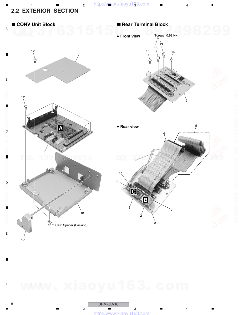
 "先锋PIONEER DRM-ULV16ZUCYVWL电路图-8")
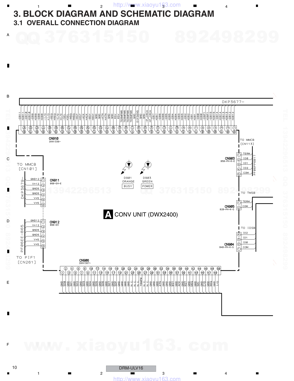 "先锋PIONEER DRM-ULV16ZUCYVWL电路图-9")
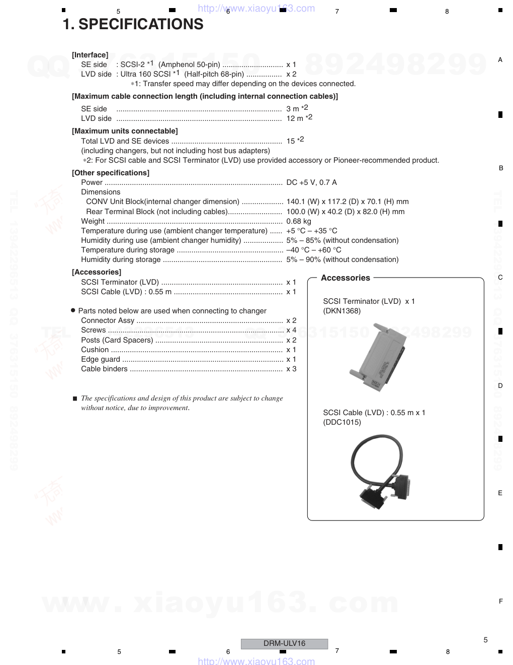
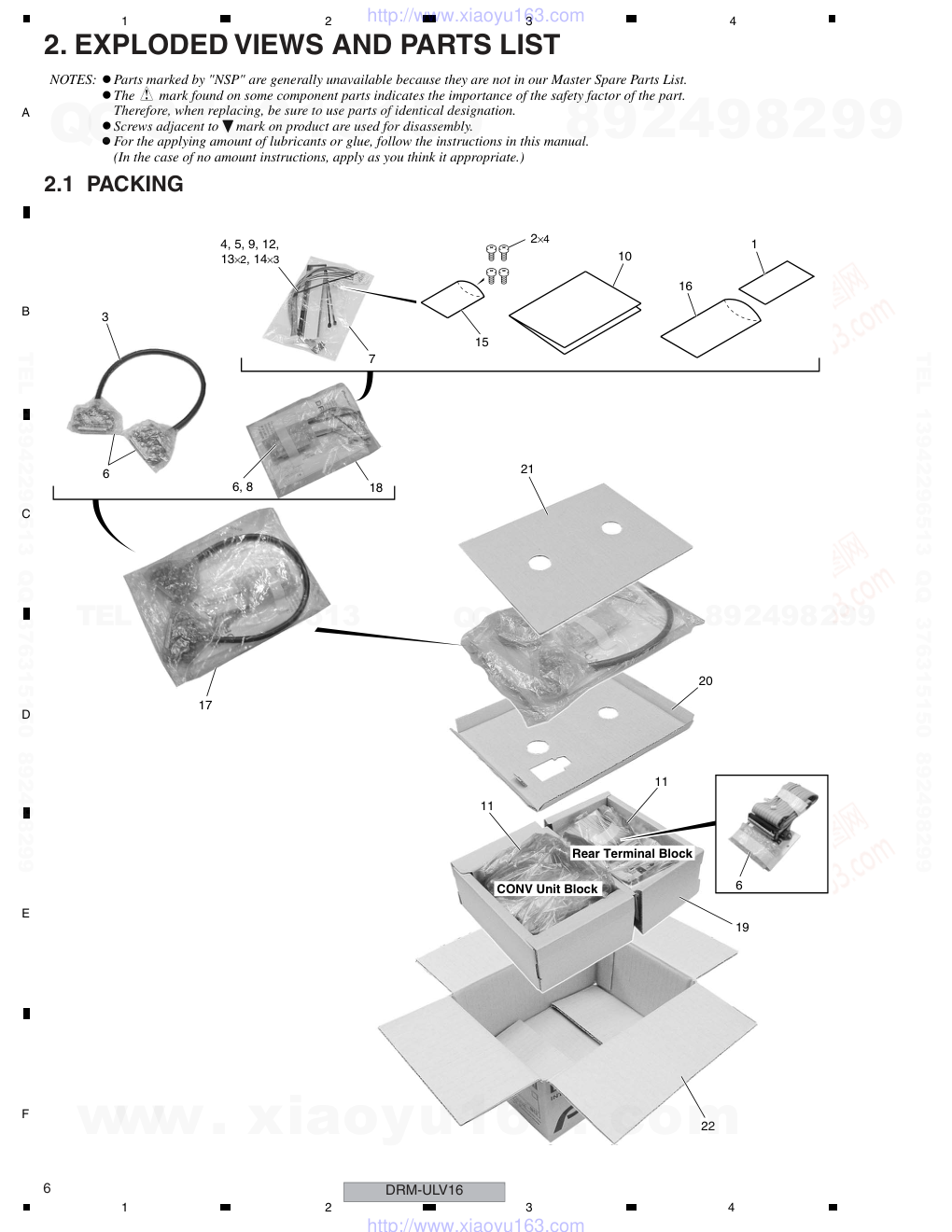
ORDER NO. PIONEER CORPORATION 4-1, Meguro 1-chome, Meguro-ku, Tokyo 153-8654, Japan PIONEER ELECTRONICS (USA) INC. P.O. Box 1760, Long Beach, CA 90801-1760, U.S.A. PIONEER EUROPE NV Haven 1087, Keetberglaan 1, 9120 Melsele, Belgium PIONEER ELECTRONICS ASIACENTRE PTE. LTD. 253 Alexandra Road, #04-01, Singapore 159936 PIONEER CORPORATION 2004 DRM-ULV16 RRV3060 LVD SCSI INTERFACE UNIT DRM-ULV16 ZUCYV/WL THIS MANUAL IS APPLICABLE TO THE FOLLOWING MODEL(S) AND TYPE(S). This service manual should be used together with the following manual(s). IMPORTANT: Before performing maintenance work or optional installation, be sure to set the power switches of the main unit and its peripheral equipment to their OFF positions, then dis- connect their power cords, in order to avoid failure of the equipment and electric shock.. Note: • If this unit is used with the DVD-R7783, the firmware version of the changer must be Ver. 1.25 or later Model Type Power Requirement Remarks DRM-ULV16 ZUCYV/WL DC Power supply from other system Model No. Order No. Remarks DRM-7000 RRV2173 700 DISC CHANGER DRM-3000 RRV2734 300 DISC CHANGER For details, refer to "Important Check Points for Good Servicing". T-ZZY DEC. 2004 printed in Japan www. xiaoyu163. com QQ 376315150 9 9 2 8 9 4 2 9 8 TEL 13942296513 9 9 2 8 9 4 2 9 8 0 5 1 5 1 3 6 7 3 Q Q TEL 13942296513 QQ 376315150 892498299 TEL 13942296513 QQ 376315150 892498299 http://www.xiaoyu163.com DRM-ULV16 2 1 2 3 4 1 2 3 4 C D F A B E SAFETY INFORMATION This service manual is intended for qualified service technicians ; it is not meant for the casual do-it- yourselfer. Qualified technicians have the necessary test equipment and tools, and have been trained to properly and safely repair complex products such as those covered by this manual. Improperly performed repairs can adversely affect the safety and reliability of the product and may void the warranty. If you are not qualified to perform the repair of this product properly and safely, you should not risk trying to do so and refer the repair to a qualified service technician. WARNING This product contains lead in solder and certain electrical parts contain chemicals which are known to the state of California to cause cancer, birth defects or other reproductive harm. Health & Safety Code Section 25249.6 – Proposition 65 www. xiaoyu163. com QQ 376315150 9 9 2 8 9 4 2 9 8 TEL 13942296513 9 9 2 8 9 4 2 9 8 0 5 1 5 1 3 6 7 3 Q Q TEL 13942296513 QQ 376315150 892498299 TEL 13942296513 QQ 376315150 892498299 http://www.xiaoyu163.com DRM-ULV16 3 5 6 7 8 5 6 7 8 C D F A B E [Important Check Points for Good Servicing] In this manual, procedures that must be performed during repairs are marked with the below symbol. Please be sure to confirm and follow these procedures. 1. Product safety Please conform to product regulations (such as safety and radiation regulations), and maintain a safe servicing environment by following the safety instructions described in this manual. 1 Use specified parts for repair. Use genuine parts. Be sure to use important parts for safety. 2 Do not perform modifications without proper instructions. Please follow the specified safety methods when modification(addition/change of parts) is required due to interferences such as radio/TV interference and foreign noise. 3 Make sure the soldering of repaired locations is properly performed. When you solder while repairing, please be sure that there are no cold solder and other debris. Soldering should be finished with the proper quantity. (Refer to the example) 4 Make sure the screws are tightly fastened. Please be sure that all screws are fastened, and that there are no loose screws. 5 Make sure each connectors are correctly inserted. Please be sure that all connectors are inserted, and that there are no imperfect insertion. 6 Make sure the wiring cables are set to their original state. Please replace the wiring and cables to the original state after repairs. In addition, be sure that there are no pinched wires, etc. 7 Make sure screws and soldering scraps do not remain inside the product. Please check that neither solder debris nor screws remain inside the product. 8 There should be no semi-broken wires, scratches, melting, etc. on the coating of the power cord. Damaged power cords may lead to fire accidents, so please be sure that there are no damages. If you find a damaged power cord, please exchange it with a suitable one. 9 There should be no spark traces or similar marks on the power plug. When spark traces or similar marks are found on the power supply plug, please check the connection and advise on secure connections and suitable usage. Please exchange the power cord if necessary. 0 Safe environment should be secured during servicing. When you perform repairs, please pay attention to static electricity, furniture, household articles, etc. in order to prevent injuries. Please pay attention to your surroundings and repair safely. 2. Adjustments To keep the original performance of the products, optimum adjustments and confirmation of characteristics within specification. Adjustments should be performed in accordance with the procedures/instructions described in this manual. 4. Cleaning For parts that require cleaning, such as optical pickups, tape deck heads, lenses and mirrors used in projection monitors, proper cleaning should be performed to restore their performances. 3. Lubricants, Glues, and Replacement parts Use grease and adhesives that are equal to the specified substance. Make sure the proper amount is applied. 5. Shipping mode and Shipping screws To protect products from damages or failures during transit, the shipping mode should be set or the shipping screws should be installed before shipment. Please be sure to follow this method especially if it is specified in this manual. www. xiaoyu163. com QQ 376315150 9 9 2 8 9 4 2 9 8 TEL 13942296513 9 9 2 8 9 4 2 9 8 0 5 1 5 1 3 6 7 3 Q Q TEL 13942296513 QQ 376315150 892498299 TEL 13942296513 QQ 376315150 892498299 http://www.xiaoyu163.com DRM-ULV16 4 1 2 3 4 1 2 3 4 C D F A B E CONTENTS SAFETY INFORMATION .............................................................................................................................. 2 1. SPECIFICATIONS ..................................................................................................................................... 5 2. EXPLODED VIEWS AND PARTS LIST ..................................................................................................... 6 2.1 PACKING............................................................................................................................................... 6 2.2 EXTERIOR SECTION ........................................................................................................................... 8 3. BLOCK DIAGRAM AND SCHEMATIC DIAGRAM ................................................................................... 10 3.1 OVERALL CONNECTION DIAGRAM ................................................................................................. 10 3.2 CONV, IDSB and TMSB UNITS........................................................................................................... 12 4. PCB CONNECTION DIAGRAM............................................................................................................... 14 4.1 CONV, IDSB and TMSB UNITS........................................................................................................... 14 5. PCB PARTS LIST..................................................................................................................................... 16 6. ADJUSTMENT......................................................................................................................................... 16 7. GENERAL INFORMATION ...................................................................................................................... 17 7.1 INSTALLATION.................................................................................................................................... 17 7.2 OPERATION CHECKS........................................................................................................................ 22 7.2.1 CHECK METHOD.......................................................................................................................... 23 7.3 IC INFORMATION ............................................................................................................................... 24 8. PANEL FACILITIES.................................................................................................................................. 27 www. xiaoyu163. com QQ 376315150 9 9 2 8 9 4 2 9 8 TEL 13942296513 9 9 2 8 9 4 2 9 8 0 5 1 5 1 3 6 7 3 Q Q TEL 13942296513 QQ 376315150 892498299 TEL 13942296513 QQ 376315150 892498299 http://www.xiaoyu163.com DRM-ULV16 5 5 6 7 8 5 6 7 8 C D F A B E 1. SPECIFICATIONS SCSI Terminator (LVD) x 1 (DKN1368) SCSI Cable (LVD) : 0.55 m x 1 (DDC1015) Accessories [Interface] SE side : SCSI-2 *1 (Amphenol 50-pin) ............................. x 1 LVD side : Ultra 160 SCSI *1 (Half-pitch 68-pin) ................. x 2 ∗1: Transfer speed may differ depending on the devices connected. [Maximum cable connection length (including internal connection cables)] SE side ............................................................................... 3 m *2 LVD side ............................................................................... 12 m *2 [Maximum units connectable] Total LVD and SE devices ..................................................... 15 *2 (including changers, but not including host bus adapters) ∗2: For SCSI cable and SCSI Terminator (LVD) use provided accessory or Pioneer-recommended product. [Other specifications] Power ..................................................................................... DC +5 V, 0.7 A Dimensions CONV Unit Block(internal changer dimension) .................... 140.1 (W) x 117.2 (D) x 70.1 (H) mm Rear Terminal Block (not including cables).......................... 100.0 (W) x 40.2 (D) x 82.0 (H) mm Weight .................................................................................... 0.68 kg Temperature during use (ambient changer temperature) ...... +5 °C – +35 °C Humidity during use (ambient changer humidity) ................... 5% – 85% (without condensation) Temperature during storage ................................................... –40 °C – +60 °C Humidity during storage ......................................................... 5% – 90% (without condensation) [Accessories] SCSI Terminator (LVD) .......................................................... x 1 SCSI Cable (LVD) : 0.55 m .................................................... x 1 Parts noted below are used when connecting to changer Connector Assy ...................................................................... x 2 Screws .................................................................................... x 4 Posts (Card Spacers) ............................................................. x 2 Cushion .................................................................................. x 1 Edge guard ............................................................................. x 1 Cable binders ......................................................................... x 3 The specifications and design of this product are subject to change without notice, due to improvement. www. xiaoyu163. com QQ 376315150 9 9 2 8 9 4 2 9 8 TEL 13942296513 9 9 2 8 9 4 2 9 8 0 5 1 5 1 3 6 7 3 Q Q TEL 13942296513 QQ 376315150 892498299 TEL 13942296513 QQ 376315150 892498299 http://www.xiaoyu163.com DRM-ULV16 6 1 2 3 4 1 2 3 4 C D F A B E 2. EXPLODED VIEWS AND PARTS LIST 2.1 PACKING Parts marked by "NSP" are generally unavailable because they are not in our Master Spare Parts List. The mark found on some component parts indicates the importance of the safety factor of the part. Therefore, when replacing, be sure to use parts of identical designation. Screws adjacent to mark on product are used for disassembly. For the applying amount of lubricants or glue, follow the instructions in this manual. (In the case of no amount instructions, apply as you think it appropriate.) NOTES: 3 18 21 20 11 19 22 11 6 15 10 16 2×4 7 4, 5, 9, 12, 13×2, 14×3 17 CONV Unit Block Rear Terminal Block 6, 8 6 1 www. xiaoyu163. com QQ 376315150 9 9 2 8 9 4 2 9 8 TEL 13942296513 9 9 2 8 9 4 2 9 8 0 5 1 5 1 3 6 7 3 Q Q TEL 13942296513 QQ 376315150 892498299 TEL 13942296513 QQ 376315150 892498299 http://www.xiaoyu163.com DRM-ULV16 7 5 6 7 8 5 6 7 8 C D F A B E PACKING Parts List Mark No. Description Part No. NSP 1 Warranty Card ARY1093 2 Screw BBZ30P060FTC 3 SCSI Cable (LVD) (55cm) DDC1015 4 Cushion (CR) DEC2707 5 Edge Guard DEC2708 NSP 6 Air Cap Bag (90 x 80) DHL1144 7 Polyethylene Bag DHL1145 (0.03 x 90 x 170) 8 SCSI Terminator (LVD) DKN1368 9 Connector Assy 6P DKP3679 10 Operating Instructions DRC1232 (English / French / German / Chinese / Japanese) 11 Polyethylene Bag PHL1004 12 Connector PF05PP6B17 13 Card Spacer QEC1012 14 Binder (SKB-90BK) ZCA-SKB90BK NSP 15 Polyethylene Bag Z21-002 (0.03 x 50 x 70) NSP 16 Polyethylene Bag Z21-010 (0.018 x 100 x 230) NSP 17 Polyethylene Bag Z21-029 (0.05 x 205 x 315) NSP 18 Polyethylene Bag Z21-038 (0.03 x 230 x 340) 19 Under Pad DHA1620 20 Upper Pad DHA1658 21 Spacer DHC1063 22 Packing Case DHG2474 www. xiaoyu163. com QQ 376315150 9 9 2 8 9 4 2 9 8 TEL 13942296513 9 9 2 8 9 4 2 9 8 0 5 1 5 1 3 6 7 3 Q Q TEL 13942296513 QQ 376315150 892498299 TEL 13942296513 QQ 376315150 892498299 http://www.xiaoyu163.com DRM-ULV16 8 1 2 3 4 1 2 3 4 C D F A B E 2.2 EXTERIOR SECTION Front view Rear view CONV Unit Block Rear Terminal Block A B C 11 1 2 8 7 5 4 9 15 13 13 14 6 16 3 10 17 Card Spacer (Packing) 12 12 Torque: 0.98 N•m www. xiaoyu163. com QQ 376315150 9 9 2 8 9 4 2 9 8 TEL 13942296513 9 9 2 8 9 4 2 9 8 0 5 1 5 1 3 6 7 3 Q Q TEL 13942296513 QQ 376315150 892498299 TEL 13942296513 QQ 376315150 892498299 http://www.xiaoyu163.com DRM-ULV16 9 5 6 7 8 5 6 7 8 C D F A B E EXTERIOR Parts List Mark No. Description Part No. 1 CONV Unit-S DXX2549 2 IDSB Unit DWS1351 3 TMSB Unit DWS1352 4 Connector Assy DKP3677 5 Connector Assy DKP3678 6 Connector Assy PF02PP-B25 7 Connector PF04PP-B32 8 IDSB Protector DEC2727 9 LVD & SE Terminal Plate DNC1710 NSP 10 CONV Board Stay DNF1702 NSP 11 CONV Heatsink DNG1091 12 Screw BBZ30P060FTC 13 HEX Screw (#4-40UNC) DBA1247 14 Screw PMH26P050FTC 15 Screw PMZ30P100FNI 16 Binder (SKB-90BK) ZCA-SKB90BK 17 LVD Connector Guard Assy DXB1826 www. xiaoyu163. com QQ 376315150 9 9 2 8 9 4 2 9 8 TEL 13942296513 9 9 2 8 9 4 2 9 8 0 5 1 5 1 3 6 7 3 Q Q TEL 13942296513 QQ 376315150 892498299 TEL 13942296513 QQ 376315150 892498299 http://www.xiaoyu163.com DRM-ULV16 10 1 2 3 4 1 2 3 4 C D F A B E 3. BLOCK DIAGRAM AND SCHEMATIC DIAGRAM 3.1 OVERALL CONNECTION DIAGRAM CONV UNIT (DWX2400) A www. xiaoyu163. com QQ 376315150 9 9 2 8 9 4 2 9 8 TEL 13942296513 9 9 2 8 9 4 2 9 8 0 5 1 5 1 3 6 7 3 Q Q TEL 13942296513 QQ 376315150 892498299 TEL 13942296513 QQ 376315150 892498299 http://www.xiaoyu163.com DRM-ULV16 11 5 6 7 8 5 6 7 8 C D F A B E ÷ When ordering service parts, be sure to refer to "EXPLODED VIEWS and PARTS LIST" or "PCB PARTS LIST". ÷ The > mark found on some component parts indicates the importance of the safety factor of the part. Therefore, when replacing, be sure to use parts of identical designation. ÷ : The power supply is shown with the marked box. IDSB UNIT (DWS1351) B TMSB UNIT (DWS1352) C TERMINAL PLATE www. xiaoyu163. com QQ 376315150 9 9 2 8 9 4 2 9 8 TEL 13942296513 9 9 2 8 9 4 2 9 8 0 5 1 5 1 3 6 7 3 Q Q TEL 13942296513 QQ 376315150 892498299 TEL 13942296513 QQ 376315150 892498299 http://www.xiaoyu163.com DRM-ULV16 12 1 2 3 4 1 2 3 4 C D F A B E 3.2 CONV, IDSB and TMSB UNITS A LDV SCSI www. xiaoyu163. com QQ 376315150 9 9 2 8 9 4 2 9 8 TEL 13942296513 9 9 2 8 9 4 2 9 8 0 5 1 5 1 3 6 7 3 Q Q TEL 13942296513 QQ 376315150 892498299 TEL 13942296513 QQ 376315150 892498299 http://www.xiaoyu163.com DRM-ULV16 13 5 6 7 8 5 6 7 8 C D F A B E A B C CONV UNIT (DWX2400) A IDSB UNIT (DWS1351) B TMSB UNIT (DWS1352) C MMCB CN113 MMCB CN114 MMCB CN101 PIF1 CN261 www. xiaoyu163. com QQ 376315150 9 9 2 8 9 4 2 9 8 TEL 13942296513 9 9 2 8 9 4 2 9 8 0 5 1 5 1 3 6 7 3 Q Q TEL 13942296513 QQ 376315150 892498299 TEL 13942296513 QQ 376315150 892498299 http://www.xiaoyu163.com DRM-ULV16 14 1 2 3 4 1 2 3 4 C D F A B E 4. PCB CONNECTION DIAGRAM 4.1 CONV, IDSB and TMSB UNITS 1 4 5 1 17 1 A U 1 26 25 27 14 13 50 1 6 1 6 1 1 2 8 1 1 5 4 3 LF 4 1 5 1 26 27 25 14 13 1 50 1 6 1 6 1 1 68 33 34 35 36 2 1 67 4 1 8 1 5 4 3 1 1 26 27 25 14 13 1 5 1 6 4 3 1 4 1 R906 CN904 R908 R907 R905 CN903 R913 R911 IC901 R914 IC907 C907 C905 TH902 CN906 R909 CN911 CN912 C908 TH903 CN905 F901 F902 C901 C909 KN904 IC902 C902 C906 D904 R912 D901 D903 R910 KN901 KN902 KN903 C916 C917 C918 C919 C920 C922 C921 C915 R920 R919 D902 TH901 CN910 CN913 X901 IC909 C927 R915 R917 C914 R916 IC908 C913 C912 F903 F904 C923 C926 C924 CN914 IC910 S901 S902 RST SEL BSY GND ATN MSG I/O REQ GND C/D ACK N.C. 1 4 POWER BUSY 4 DNX2593-A 1 PC TERM ID0 1 ID1 1 DWX2400-A V+5 GND5 GND5 V+12 GND12 V+5 COM TERM ID2 COM COM ID2 ID1 ID0 TRMPW N.C. GND GND SDP SD7 SD6 SD5 GND SD4 SD3 SD2 SD1 SD0 ICT FC CONV TRMPW N.C. GND N.C. GND GND GND GND GND GND GND GND GND GND GND GND GND GND GND GND GND GND GND GND 1 3 4 2 26 1 13 14 25 27 CONV UNIT A TMSB UNIT C IDSB UNIT B MMCB CN114 CN906 MMCB CN101 CN911 PIF1 CN261 CN912 MMCB CN113 CN903 LVD SCSI (DNP2118-A) IC902 IC901 IC909 IC908 TH903 TH902 IC907 IC910 (DNP2118-A) (DNP2118-A) CN910 CN913 CN914 CN904 CN905 A B C A B C NOTE FOR PCB DIAGRAMS : 1. Part numbers in PCB diagrams match those in the schematic diagrams. 2. A comparison between the main parts of PCB and schematic diagrams is shown below. 3. The parts mounted on this PCB include all necessary parts for several destinations. For further information for respective destinations, be sure to check with the schematic diagram. 4. View point of PCB diagrams. Symbol In PCB Diagrams Symbol In Schematic Diagrams Part Name B C E D D G G S S B C E B C E D G S B C E B C E B C E Transistor Transistor with resistor Field effect transistor Resistor array 3-terminal regulator Capacitor Connector P.C.Board Chip Part SIDE A SIDE B www. xiaoyu163. com QQ 376315150 9 9 2 8 9 4 2 9 8 TEL 13942296513 9 9 2 8 9 4 2 9 8 0 5 1 5 1 3 6 7 3 Q Q TEL 13942296513 QQ 376315150 892498299 TEL 13942296513 QQ 376315150 892498299 http://www.xiaoyu163.com DRM-ULV16 15 5 6 7 8 5 6 7 8 C D F A B E 4 1 5 1 1 50 1 6 6 1 4 1 LF LF LF 1 -DB11 -DB1 -DBP1 -DB14 68 2 1 36 34 33 35 67 -ATN -DB10 RSV TERMPWR -DB7 -DB5 -DB3 N.C. N.C. GND -I/O -DB8 -BSY -RST -SEL GND -ACK -REQ GND GND GND GND +P_CRCA DIFSENS TERMPWR GND C/D GND GND GND GND GND GND GND GND GND GND GND GND GND N.C. N.C. SD1 GND +DB13 +DB15 +DB0 +DB2 +DB4 +DB6 GND +ACK +MSG +C/D +I/O +DB9 +DB11 +DB12 +DB14 +DBP1 +DB1 +DB3 DNX2595-A SD7 SD4 SD6 SD3 SD2 SD0 GND REQ GND GND +DB5 +DB7 GND TERMPWR RSV +ATN +BSY +RST +SEL +REQ +DB8 +DB10 GND -DB15 -DB13 TERM DWS1352-A TMSB DNX2594-A DWS1351-A IDSB SDP GND N.C. GND I/O GND ATN GND BSY ACK RST MSG SEL TRMPW SD5 GND12 V+12 GND5 GND5 V+5 V+5 GND12 V+12 GND5 GND5 V+5 GND V+5 COM ID2 ID1 ID0 TERM COM ID0 ID1 ID2 COM -MSG TERM -C/D -DB12 -DB9 GND -P_CRCA -DB0 -DB6 -DB4 -DB2 TERMPWR ID2 ID1 ID0 COM COM CONV UNIT A TMSB UNIT C IDSB UNIT B CN906 CN911 CN912 CN903 (DNP2118-A) (DNP2118-A) (DNP2118-A) CN910 CN913 CN914 CN904 CN905 A B C A B C www. xiaoyu163. com QQ 376315150 9 9 2 8 9 4 2 9 8 TEL 13942296513 9 9 2 8 9 4 2 9 8 0 5 1 5 1 3 6 7 3 Q Q TEL 13942296513 QQ 376315150 892498299 TEL 13942296513 QQ 376315150 892498299 http://www.xiaoyu163.com DRM-ULV16 16 1 2 3 4 1 2 3 4 C D F A B E 5. PCB PARTS LIST 6. ADJUSTMENT • There is no information to be shown in this chapter. Parts marked by "NSP" are generally unavailable because they are not in our Master Spare Parts List. The mark found on some component parts indicates the importance of the safety factor of the part. Therefore, when replacing, be sure to use parts of identical designation. When ordering resistors, first convert resistance values into code form as shown in the following examples. Ex.1 When there are 2 effective digits (any digit apart from 0), such as 560 ohm and 47k ohm (tolerance is shown by J=5%, and K=10%). Ex.2 When there are 3 effective digits (such as in high precision metal film resistors). 5 6 1 4 7 3 R 5 0 1 R 0 5 6 2 1 NOTES: 560 Ω 47k Ω 0.5 Ω 1 Ω RD1/4PU J RD1/4PU J RN2H K RS1P K 56 x 10 1 47 x 10 3 R50 1R0 561 473 5.62k Ω RN1/4PC F 562 x 10 1 5621 Mark No. Description Part No. LIST OF ASSEMBLIES NSP 1..CVSW UNIT DWM2184 2..IDSB UNIT DWS1351 2..TMSB UNIT DWS1352 NSP 2..CONV UNIT DWX2400 Mark No. Description Part No. A CONV UNIT SEMICONDUCTORS IC907,IC910 BH9598AFP-Y IC901 LSI53C180-192BGA-K > IC902 PQ3DZ13 IC908 S-80945CNMC-G9F IC909 TC7WU04F D902,D904 RB160L-40 D901 SML-210DT D903 SML-210MT > TH901 MINISMDC100F > TH903 MINISMDC160F COILS AND FILTERS F901-F904 EMI FILTER DTF1106 CAPACITORS C909 CEHVW101M6R3 C906,C908 CEHVW470M6R3 C915 CKSRYB103K50 C901,C902,C905,C907 CKSRYB104K25 C913,C914,C916-C923 CKSRYB104K25 C926,C927 CKSRYB104K25 RESISTORS All Resistors RS1/16S###J OTHERS CN905 KR CONNECTOR B2B-PH-K-S CN904 KR CONNECTOR B4B-PH-K-S CN903 KR CONNECTOR B5B-PH-K-E CN912 6P TOP POST B6B-EH CN911 6P TOP POST B6B-EH-E CN910 SCSI CONNECTOR (68P) DKN1336 CN906 RX HEADER DKN1367 X901 CERAMIC RESONATOR DSS1151 KN901-KN904 EARTH METAL FITTING VNF1109 B IDSB UNIT SWITCHES S901 DSX1043 OTHERS 0 ID SWITCH HOLDER DEC1805 CN913 KR CONNECTOR S4B-PH-K-S C TMSB UNIT SWITCHES S902 DSH1057 OTHERS CN914 KR CONNECTOR S2B-PH-K-S Mark No. Description Part No. www. xiaoyu163. com QQ 376315150 9 9 2 8 9 4 2 9 8 TEL 13942296513 9 9 2 8 9 4 2 9 8 0 5 1 5 1 3 6 7 3 Q Q TEL 13942296513 QQ 376315150 892498299 TEL 13942296513 QQ 376315150 892498299 http://www.xiaoyu163.com DRM-ULV16 17 5 6 7 8 5 6 7 8 C D F A B E 7. GENERAL INFORMATION 7.1 INSTALLATION The DRM-ULV16 is an optional SCSI Board Unit for the DRM-7000 and DRM-3000 Changer System. How to install this unit in the changer system is described in this section. The photos and/or illustrations of the DRM-ULV16 and the changer in this manual may differ from those of your product, but the installation procedures are the same. The photos and illustrations of the changer system in this manual are those of the DRM-7000, unless otherwise stated. 1 Remove the four screws that secure the side panel. The side panel is located at the lower right side on the DRM-7000, and at the right side on the DRM-3000. 2 Remove the side panel. Removal of the side panel 1 1 Cut the binder to unbind the wires. 2 Disconnect the cables from the connector for the power (CN101_6P) and the connector for the ID and terminating switch (CN113_5P) on the MMCB unit. 3 Except for the wires for the connectors disconnected in Step 2, bind the wires using the supplied binder as they were. Note: Care must be taken not to damage the wires. MMCB Unit CN101 CN113 Removal of the rear terminal block 2 1 1 2 3 2 1 1 2 1 Preparations on the side of the changer Note: If this unit is used with the DVD-R7783, the firmware version of the changer must be Ver. 1.25 or later. www. xiaoyu163. com QQ 376315150 9 9 2 8 9 4 2 9 8 TEL 13942296513 9 9 2 8 9 4 2 9 8 0 5 1 5 1 3 6 7 3 Q Q TEL 13942296513 QQ 376315150 892498299 TEL 13942296513 QQ 376315150 892498299 http://www.xiaoyu163.com DRM-ULV16 18 1 2 3 4 1 2 3 4 C D F A B E Cable clamp 4 Disconnect the flat cable from the CN114 connector on the MMCB unit then unhook the flat cable clamp to free the flat cable from it. 5 Unhook the cable clamp to free the Connector Assy (5P) for the ID and terminating switch. 6 Remove the four screws at the rear then remove the rear terminal block. (Be sure to keep the screws, as you will need them later.) 1 Tie the wires around the SIFB2 unit with the supplied binder. 2 Attach the supplied edge guard. Note: Bind the wires in a way that allows a clear space around here, so that the wires will not be snagged when installing this unit. Flat cable clamp Connector Assy (5P) MMCB Unit SIFB2 Unit SIFB2 Unit CN114 Preparation for installation 3 4 5 1 4 6 6 6 6 2 6 Rear terminal block Rear terminal block Edge guard Edge guard www. xiaoyu163. com QQ 376315150 9 9 2 8 9 4 2 9 8 TEL 13942296513 9 9 2 8 9 4 2 9 8 0 5 1 5 1 3 6 7 3 Q Q TEL 13942296513 QQ 376315150 892498299 TEL 13942296513 QQ 376315150 892498299 http://www.xiaoyu163.com DRM-ULV16 19 5 6 7 8 5 6 7 8 C D F A B E 1 Unpack the CONV unit block. Set aside the LVD connector guard Assy. 2 Attach the two supplied card spacers. 3 Temporarily install the CONV unit block in the changer in order to check if it interferes with the card spacer or not. 5 Adhere the supplied cushion. 4 Check the position of the flat cable clamp and determine the location where the cushion is to be adhered. Remove the temporarily installed CONV unit block. (Leave the flat cable clamp in place.) Reference line (left side of the flat cable clamp) Remove the temporarily installed CONV unit block then remove the flat cable clamp. Flat cable clamp Flat cable clamp Flat cable clamp Card spacer Card spacer Cushion Cushion CONV unit block CONV unit block A) In a case where the flat cable clamp is located at the right of the right card spacer and does not get in the way of it B) In a case where the flat cable clamp is located at the left of the right card spacer or gets in the way of it LVD connector guard Assy Card spacer Preparation for installation 4 Installation of the DRM-ULV16 CONV unit block Before attachment Install the CONV unit block so that the protruding screws a are inserted through the elliptical holes b ( ). After attachment CONV unit block CONV unit block Card spacer 1 a a b b 2 2 5 Engraved mark 5 Bottom view Reference line (right side of the engraved mark) www. xiaoyu163. com QQ 376315150 9 9 2 8 9 4 2 9 8 TEL 13942296513 9 9 2 8 9 4 2 9 8 0 5 1 5 1 3 6 7 3 Q Q TEL 13942296513 QQ 376315150 892498299 TEL 13942296513 QQ 376315150 892498299 http://www.xiaoyu163.com DRM-ULV16 20 1 2 3 4 1 2 3 4 C D F A B E 1 Unpack the rear terminal block. 2 Pass the wires through the opening first, then secure the block using the four screws that were removed in Step ø-6. Installation of the rear terminal block 5 2 2 1 2 Rear terminal block Rear terminal block Flat cable clamp Flat cable (GRN/GRY) Flat cable (GRN/GRY) CONV unit block CONV unit block 2 2 3 2 Note: Care must be taken not to bump the board against the plate during attachment. Note: Be careful not to damage the wires with the sharp edge of the plate when you pass the wires through the opening. Note: Care must be taken not to snag the wires. (See Step π-1.) Note: Be careful that the card spacers do not press against the flat cable (GRN/GRY). 1 Unhook the flat cable clamp and fix the flat cable (GRN/GRY) with it. (If the flat cable clamp has been removed in Step [-4, go to the next step.) 2 Set the CONV unit block in place, referring to Step [-3. 3 Secure the block in place with the three supplied screws, in the order indicated below (Center Left Right). Installation of the CONV unit block 6 -1 3 -2 3 -3 IDSB Unit Note: While disassembling/reassembling the IDSB unit, be careful not to apply any external pressure on it, including on the parts specifically mentioned in the instructions. www. xiaoyu163. com QQ 376315150 9 9 2 8 9 4 2 9 8 TEL 13942296513 9 9 2 8 9 4 2 9 8 0 5 1 5 1 3 6 7 3 Q Q TEL 13942296513 QQ 376315150 892498299 TEL 13942296513 QQ 376315150 892498299 http://www.xiaoyu163.com DRM-ULV16 21 5 6 7 8 5 6 7 8 C D F A B E 4 Connect the flat cables. 5 Set the LVD connector guard Assy in place then secure it with the supplied screw. 6 Unhook the cable clamp and bind the Connector Assy (4P) for the ID and the Connector Assy (2P) for the terminating switch together with it. 4 4 4 7 7 7 8 8 8 8 5 9 5 6 Flat cable (GRN/GRY) Flat cable (ORG/WHT) LVD connector guard Assy Cable clamp Connector Assy (2P) Connector Assy (4P) Shaft Drilled hole CONV Unit CONV Unit CONV Unit CONV Unit MMCB Unit MMCB Unit CN114 CN906 CN910 CN912 CN911 CN903 CN101 CN113 CN904 CN905 Note: Be sure to connect the tagged side of the flat cable (GRN/GRY) to the CN114 on the MMCB unit. While plugging in the connector, hold the rear of the MMCB unit so that the board will not bend. Note: Be sure to pass the shaft through the flat cable (ORG/WHT) then insert the end of it into the drilled hole of the panel. After confirming that the end of the shaft is securely inserted in the drilled hole, tighten the screw. Note: Bind the wires at as far up as possible. 7 Connect the cables to the connector for the ID (CN904_4P), the Connector for the terminating switch (CN905_2P), and the connector for the power (CN912_6P). 8 Connect the CN113 on the MMCB unit and the CN903 on the CONV unit using the supplied Connector Assy (5P), as well as the CN101 on the MMCB unit and CN911 on the CONV unit using the supplied Connector Assy (6P). 9 Bind the wires with the supplied binder. 10 Reattach the side panel of the changer. Flat cable (ORG/WHT) Connector Assy (6P) Connector Assy (5P) www. xiaoyu163. com QQ 376315150 9 9 2 8 9 4 2 9 8 TEL 13942296513 9 9 2 8 9 4 2 9 8 0 5 1 5 1 3 6 7 3 Q Q TEL 13942296513 QQ 376315150 892498299 TEL 13942296513 QQ 376315150 892498299 http://www.xiaoyu163.com DRM-ULV16 22 1 2 3 4 1 2 3 4 C D F A B E 7.2 OPERATION CHECKS Top view ON OFF Function switches Note: Be sure to perform the following operation checks after installation or repair. 7 Things required for operation checks • GGS1030: DiagnoseV (use the version 2.900 or later) • GGV1035: DVD-ROM (Single/DVDT-001) • DVD-D7362/DVD-D7563 • Personal computer ∗: SCSI data must be checked via the DRM-ULV16, as shown in Fig.1 "Connection example" below. ∗: On the DVD-D7563 or DVD-D7362, the SCSI mode must be set to SCSI-3, as shown in Fig.2. When the SCSI mode setting was changed, return the switch setting to the original after checking. Fig.1: Connection example Fig.2: Function switches These switches are used for inspection before shipment. Do NOT change the settings. SCSI mode select switch OFF (SCSI-2 mode): Burst transfer rate 10 MByte/sec ON (SCSI-3 mode): Burst transfer rate 20 MByte/sec ∗: Upon shipment, the switch is set to OFF (SCSI-2 mode). www. xiaoyu163. com QQ 376315150 9 9 2 8 9 4 2 9 8 TEL 13942296513 9 9 2 8 9 4 2 9 8 0 5 1 5 1 3 6 7 3 Q Q TEL 13942296513 QQ 376315150 892498299 TEL 13942296513 QQ 376315150 892498299 http://www.xiaoyu163.com DRM-ULV16 23 5 6 7 8 5 6 7 8 C D F A B E 7.2.1 CHECK METHOD With this method, operation checks for the DRM-ULV16 are performed by checking the transfer rate using the DVD-D7563 or DVD-D7362. Note: Use the ASC-29160 or ASC-39160 SCSI card by Adaptec as a host bus adaptor for this checking method. 1. Start up GGS1030 (DiagnoseV), and load the GGV1035 (DVDT-001) in the drive. 2. Select "Data Transfer Rate" (1), specify "220000h (HEX: hexadecimal)" to "Address" (2), then click on the "Diag" button (3). 3. The notice is displayed to prompt you to check that the drive is set to SCSI-3 mode. If the "OK" button (4) is clicked on after checking, measurement of the data transfer rate starts. 4. Check that the result (5) is "Judge: OK". ¶ If the result is NG, check the following: • Is the SCSI cable properly connected? • Is the SCSI mode correctly set to SCSI-3? • Is the termination setting correct? ¶ After checking the above items, turn off the changer, correct any wrong settings, then retry this check method from the beginning (power ON). 1 1 2 3 2 4 www. xiaoyu163. com QQ 376315150 9 9 2 8 9 4 2 9 8 TEL 13942296513 9 9 2 8 9 4 2 9 8 0 5 1 5 1 3 6 7 3 Q Q TEL 13942296513 QQ 376315150 892498299 TEL 13942296513 QQ 376315150 892498299 http://www.xiaoyu163.com DRM-ULV16 24 1 2 3 4 1 2 3 4 C D F A B E 7.3 IC INFORMATION LSI53C180-192BGA-K (CONV UNIT: IC901) • SCSI Expander IC Retiming Logic Precision Delay Control State Machine Control LVD DIFFSENS Receiver LVD DIFFSENS Receiver SCSI Control Block SCSI Control Block LVD Link Transceivers LVD Link Transceivers Control Signals LVD, Single-ended, Wide Ultra SCSI Bus (A Side) LVD, Single-ended Wide Ultra SCSI Bus (B Side) A_DIFFSENS B_DIFFSENS 40 MHz Clock Input A1 A2 A3 A4 A5 A6 A7 A8 A9 NC VDDIO NC NC NC XFER_ACTIVE RESET/ A_DIFFSENS A_SD12- B1 B2 B3 B4 B5 B6 B7 B8 B9 B_SD11+ B_SD11- NC NC WS_ENABLE/ BSY_LED NC VDDCORE A_SD12+ C1 C2 C3 C4 C5 C6 C7 C8 C9 B_SD10+ B_SD10- B_DIFFSENS NC VDDSCSI NC VSS CLOCK VDDSCSI D1 D2 D3 B_SD9+ B_SD9- NC E1 E2 E3 B_SD8+ B_SD8- VDDSCSI F1 F2 F3 B_SIO+ B_SIO- NC G1 G2 G3 G7 G8 G9 B_SREQ+ B_SREQ- VSS VSS VSS VSS H1 H2 H3 H7 H8 H9 B_SCD- B_SSEL+ B_SCD+ VSS VSS VSS J1 J2 J3 J7 J8 B_SSEL- B_SMSG+ VDDSCSI VSS VSS K1 K2 K3 K7 K8 K9 B_SMSG- B_SRST+ VDDCORE VSS VSS VSS L1 L2 L3 L7 L8 L9 B_SRST- NC VSS VSS VSS VSS M1 M2 M3 B_SACK+ B_SACK- B_SBSY+ N1 N2 N3 B_SBSY- B_SATN+ VDDSCSI P1 P2 P3 B_SATN- B_SDP0- B_SDP0+ R1 R2 R3 R4 R5 R6 R7 R8 R9 B_RBIAS B_SD7+ B_SD7- NC VDDSCSI B_SD2+ VSS B_SD0- VDDSCSI T1 T2 T3 T4 T5 T6 T7 T8 T9 NC B_SD6+ B_SD5+ B_SD4+ B_SD3+ B_SD2- B_SD1+ B_SD0+ B_SDP1+ U1 U2 U3 U4 U5 U6 U7 U8 U9 NC B_SD6- B_SD5- B_SD4- B_SD3- NC B_SD1- VDDCORE B_SDP1- A10 A11 A12 A13 A14 A15 A16 A17 A_SD13- A_SD14+ A_SD15+ A_SD0- A_SD1- A_SD2- A_SD3- NC B10 B11 B12 B13 B14 B15 B16 B17 A_SD14- A_SD15- A_SDP1- A_SD0+ A_SD1+ A_SD2+ A_SD3+ A_SD4- C10 C11 C12 C13 C14 C15 C16 C17 A_SD13+ VSS A_SDP1+ VDDSCSI NC NC A_SD5- A_SD4+ D15 D16 D17 A_SD5+ A_SD6+ A_SD6- E15 E16 E17 VDDSCSI A_SD7+ A_SD7- F15 F16 F17 NC A_SDP0+ A_SDP0- G10 G11 G15 G16 G17 VSS VSS VSS A_SATN+ A_SATN- H10 H11 H15 H16 H17 VSS VSS NC A_SBSY+ A_SBSY- J10 J11 J15 J16 J17 VSS VSS VDD A_SACK+ A_SACK- K10 K11 K15 K16 K17 VSS VSS VDDCORE A_SRST- A_RBIAS L10 L11 L15 L16 L17 VSS VSS VSS A_SMSG- A_SRST+ M15 M16 M17 A_SSEL+ A_SSEL- A_SMSG+ N15 N16 N17 VDDSCSI A_SCD+ A_SCD- P15 P16 P17 NC A_SREQ+ A_SREQ- R10 R11 R12 R13 R14 R15 R16 R17 NC VSS NC VDDSCSI A_SD10+ A_SD9- A_SIO+ A_SIO- T10 T11 T12 T13 T14 T15 T16 T17 B_SD15+ B_SD14+ B_SD13+ B_SD12+ A_SD11+ A_SD10- A_SD8+ A_SD8- U10 U11 U12 U13 U14 U15 U16 U17 B_SD15- B_SD14- B_SD13- B_SD12- A_SD11- A_SD9+ NC NC A_SSEL+ A_SSEL- A_SBSY+ A_SBSY- A_SRST+ A_SRST- A_SREQ+ A_SREQ- A_SACK+ A_SACK- A_SMSG+ A_SMSG- A_SCD+ A_SCD- A_SIO+ A_SIO- A_SATN+ A_SATN- A_SDP[1:0]+ A_SDP[1:0]- A_SD[15:0]+ A_SD[15:0]- A_DIFFSENS B_SSEL+ B_SSEL- B_SBSY+ B_SBSY- B_SRST+ B_SRST- B_SREQ+ B_SREQ- B_SACK+ B_SACK- B_SMSG+ B_SMSG- B_SCD+ B_SCD- B_SIO+ B_SIO- B_SATN+ B_SATN- B_SDP[1:0]+ B_SDP[1:0]- B_SD[15:0]+ B_SD[15:0]- B_DIFFSENS A Side LVD or SE SCSI Interface B Side LVD or SE SCSI Interface Control Signals LSI53C180 RESET/ WS_ENABLE BSY_LED XFER_ACTIVE CLOCK A_RBIAS B_RBIAS Pin Arrangement (Top view) Block diagram • The information shown in the list is basic information and may not correspond exactly to that shown in the schematic diagrams. www. xiaoyu163. com QQ 376315150 9 9 2 8 9 4 2 9 8 TEL 13942296513 9 9 2 8 9 4 2 9 8 0 5 1 5 1 3 6 7 3 Q Q TEL 13942296513 QQ 376315150 892498299 TEL 13942296513 QQ 376315150 892498299 http://www.xiaoyu163.com DRM-ULV16 25 5 6 7 8 5 6 7 8 C D F A B E SCSI A BGA Pin Type Description A_SSEL+,- M15, M16 I/O A Side SCSI bus Select control signal. A_SBSY+,- H16, H17 I/O A Side SCSI bus Busy control signal. A_SRST+,- L17, K16 I/O A Side SCSI bus Reset control signal. A_SREQ+,- P16, P17 I/O A Side SCSI bus Request control signal. A_SACK+,- J16, J17 I/O A Side SCSI bus Acknowledge control signal. A_SMSG+,- M17, L16 I/O A Side SCSI bus Message control signal. A_SCD+,- N16, N17 I/O A Side SCSI bus Control and Data control signal. A_SIO+,- R16, R17 I/O A Side SCSI bus Input and Output control signal. A_SATN+,- G16, G17 I/O A Side SCSI bus Attention control signal. A_SDP[1:0]+,- C12, B12, F16, F17 I/O A Side SCSI bus Data Parity signal. A_SD[15:0]+,- A12, B11, A11, B10, C10, A10, B9, A9, T14, U14, R14, T15, U15, R15, T16, T17, E16, E17, D16, D17, D15, C16, C17, B17, B16, A16, B15, A15, B14, A14, B13, A13 I/O A Side SCSI bus Data signals. A_DIFFSENS A8 I A Side SCSI bus Differential Sense signal. A_RBIAS K17 RBIAS LVD current control. SCSI B Side Interface Pins SCSI B Pin Type Description B_SSEL+,- H2, J1 I/O B Side SCSI bus Select control signal. B_SBSY+,- M3, N1 I/O B Side SCSI bus Busy control signal. B_SRST+,- K2, L1 I/O B Side SCSI bus Reset control signal. B_SREQ+,- G1, G2 I/O B Side SCSI bus Request control signal. B_SACK+,- M1, M2 I/O B Side SCSI bus Acknowledge control signal. B_SMSG+,- J2, K1 I/O B Side SCSI bus Message control signal. B_SCD+,- H3, H1 I/O B Side SCSI bus Control and Data control signal. B_SIO+,- F1, F2 I/O B Side SCSI bus Input and Output control signal. B_SATN+,- N2, P1 I/O B Side SCSI bus Attention control signal. B_SDP[1:0]+,- T9, U9, P3, P2 I/O B Side SCSI bus Data Parity signal. B_SD[15:0]+,- T10, U10, T11, U11, T12, U12, T13, U13, B1, B2, C1, C2, D1, D2, E1, E2, R2, R3, T2, U2, T3, U3, T4, U4, T5, U5, R6, T6, T7, U7, T8, R8 I/O B Side SCSI bus Data signals. B_DIFFSENS C3 I B Side SCSI bus Differential Sense signal. B_RBIAS R1 RBIAS LVD current control. SCSI A Side Interface Pins Pin Function (1/2) www. xiaoyu163. com QQ 376315150 9 9 2 8 9 4 2 9 8 TEL 13942296513 9 9 2 8 9 4 2 9 8 0 5 1 5 1 3 6 7 3 Q Q TEL 13942296513 QQ 376315150 892498299 TEL 13942296513 QQ 376315150 892498299 http://www.xiaoyu163.com DRM-ULV16 26 1 2 3 4 1 2 3 4 C D F A B E Power and Ground Pins Power and Ground Pin Type Description VDDSCSI C5, C9, C13, E3, E15, J3, J15, N3, N15, R5, R9, R13 I Power supplies to the SCSI bus I/O pins. VDDCORE B8, K3, K15, U8 I Power supplies to the CORE logic. VDDIO A2 I Power supplies to the I/O logic. VSS C7, C11, G3, G7, G8, G9, G10, G11, G15, H7, H8, H9, H10, H11, J7, J8, J10, J11, K7, K8, K9, K10, K11, L3, L7, L8, L9, L10, L11, L15, R7, R11 I Ground ring. NC A1, A3, A4, A5, A17, B3, B4, B7, C4, C6, C14, C15, D3, F3, F15, H15, L2, P15, R4, R10, R12, T1, U1, U6, U16, U17 N/A No Connections. Chip Interface Control Pins Control Pin Type Description RESET/ A7 I Master Reset for LSI53C180, active LOW. WS_ENABLE/ B5 I Enable/disable SCSI transfers through the LSI53C180. XFER_ACTIVE A6 O Transfers through the LSI53C180 are enabled/disabled. CLOCK C8 I Oscillator input for LSI53C180 (40 MHz). BSY_LED B6 O SCSI activity LED output, 8 mA. Pin Function (2/2) www. xiaoyu163. com QQ 376315150 9 9 2 8 9 4 2 9 8 TEL 13942296513 9 9 2 8 9 4 2 9 8 0 5 1 5 1 3 6 7 3 Q Q TEL 13942296513 QQ 376315150 892498299 TEL 13942296513 QQ 376315150 892498299 http://www.xiaoyu163.com DRM-ULV16 27 5 6 7 8 5 6 7 8 C D F A B E 8. PANEL FACILITIES SE SCSI termination switch (CHANGER) Use to set changer’s SCSI terminator ON/OFF. Factory default: ON SCSI ID switch (CHANGER) Use to set the changer’s SCSI ID. Pressing the upper protrusion causes the number to decrement, while pressing the lower protrusion increments the number. Factory default: 6 LVD SCSI interface connector Connect using the supplied (or optionally purchased) SCSI Cable (LVD), or supplied SCSI Terminator (LVD). SE SCSI interface connector Connect to the changer’s supplied SCSI Cable (SE). Note: Avoid touching the connectors, since faulty connection or damage from static electricity may result. 1 2 3 4 Rear Connectors 1 2 3 4 www. xiaoyu163. com QQ 376315150 9 9 2 8 9 4 2 9 8 TEL 13942296513 9 9 2 8 9 4 2 9 8 0 5 1 5 1 3 6 7 3 Q Q TEL 13942296513 QQ 376315150 892498299 TEL 13942296513 QQ 376315150 892498299 http://www.xiaoyu163.com DRM-ULV16 28 1 2 3 4 1 2 3 4 C D F A B E JIGS List JIG No. JIG Name Remarks GGS1030 DiagnoseV GGV1035 DVD-ROM (Single/DVDT-001) DVD-D7362/DVD-D7563 Personal Computer www. xiaoyu163. com QQ 376315150 9 9 2 8 9 4 2 9 8 TEL 13942296513 9 9 2 8 9 4 2 9 8 0 5 1 5 1 3 6 7 3 Q Q TEL 13942296513 QQ 376315150 892498299 TEL 13942296513 QQ 376315150 892498299 http://www.xiaoyu163.com
版权声明
1. 本站所有素材,仅限学习交流,仅展示部分内容,如需查看完整内容,请下载原文件。
2. 会员在本站下载的所有素材,只拥有使用权,著作权归原作者所有。
3. 所有素材,未经合法授权,请勿用于商业用途,会员不得以任何形式发布、传播、复制、转售该素材,否则一律封号处理。
4. 如果素材损害你的权益请联系客服QQ:77594475 处理。