先锋PIONEER DEH-P6400RXN电路图
 "先锋PIONEER DEH-P6400RXN电路图-0")
 "先锋PIONEER DEH-P6400RXN电路图-1")
 "先锋PIONEER DEH-P6400RXN电路图-2")
 "先锋PIONEER DEH-P6400RXN电路图-3")
 "先锋PIONEER DEH-P6400RXN电路图-4")
 "先锋PIONEER DEH-P6400RXN电路图-5")
 "先锋PIONEER DEH-P6400RXN电路图-6")
 "先锋PIONEER DEH-P6400RXN电路图-7")
 "先锋PIONEER DEH-P6400RXN电路图-8")
 "先锋PIONEER DEH-P6400RXN电路图-9")
PIONEER CORPORATION
4-1, Meguro 1-Chome, Meguro-ku, Tokyo 153-8654, Japan
PIONEER ELECTRONICS (USA) INC.
P.O.Box 1760, Long Beach, CA 90801-1760 U.S.A.
PIONEER EUROPE NV
Haven 1087 Keetberglaan 1, 9120 Melsele, Belgium
PIONEER ELECTRONICS ASIACENTRE PTE.LTD.
253 Alexandra Road, #04-01, Singapore 159936
C PIONEER CORPORATION 2001
K-ZZY. DEC. 2001 Printed in Japan
DEH-P6400R
XN/EW
- This service manual should be used together with the following manual(s):
Model No.
Order No.
Mech. Module Remarks
CX-977
CRT2624
S9
CD Mech. Module:Circuit Description, Mech.Description, Disassembly
CONTENTS
1. SAFETY INFORMATION ............................................3
2. EXPLODED VIEWS AND PARTS LIST.......................4
3. BLOCK DIAGRAM AND SCHEMATIC DIAGRAM ...10
4. PCB CONNECTION DIAGRAM ................................24
5. ELECTRICAL PARTS LIST ........................................32
6. ADJUSTMENT..........................................................38
7. GENERAL INFORMATION .......................................47
7.1 DIAGNOSIS ........................................................47
7.1.1 DISASSEMBLY .........................................47
7.1.2 CONNECTOR FUNCTION DESCRIPTION.......51
7.2 IC ........................................................................52
7.3 OPERATIONAL FLOW CHART...........................62
7.4 CLEANING ..........................................................63
8. OPERATIONS AND SPECIFICATIONS.....................64
For details, refer to "Important symbols for good services".
ORDER NO.
CRT2806
MULTI-CD/DAB CONTROL HIGH POWER CD PLAYER WITH RDS TUNER
Service
Manual
www. xiaoyu163. com
QQ 376315150
9
9
2
8
9
4
2
9
8
TEL 13942296513
9
9
2
8
9
4
2
9
8
0
5
1
5
1
3
6
7
3
Q
Q
TEL 13942296513 QQ 376315150 892498299
TEL 13942296513 QQ 376315150 892498299
http://www.xiaoyu163.com
2
DEH-P6400R
- CD Player Service Precautions
1. For pickup unit(CXX1480) handling, please refer
to"Disassembly"(see page 47)
During replacement, handling precautions shall be
taken to prevent an electrostatic discharge(protection
by a jumper-solder).
2. During disassembly, be sure to turn the power off
since an internal IC might be destroyed when a con-
nector is plugged or unplugged.
3. Please checking the grating after changing the ser-
vice pickup unit(see page 41).
[ Important symbols for good services ]
In this manual, the symbols shown-below indicate that adjustments, settings or cleaning should be made securely.
When you find the procedures bearing any of the symbols, be sure to fulfill them:
2. Adjustments
To keep the original performances of the product, optimum adjustments or specification confirmation is indispensable.
In accordance with the procedures or instructions described in this manual, adjustments should be performed.
3. Cleaning
For optical pickups, tape-deck heads, lenses and mirrors used in projection monitors, and other parts requiring cleaning,
proper cleaning should be performed to restore their performances.
5. Lubricants, glues, and replacement parts
Appropriately applying grease or glue can maintain the product performances. But improper lubrication or applying
glue may lead to failures or troubles in the product. By following the instructions in this manual, be sure to apply the
prescribed grease or glue to proper portions by the appropriate amount.For replacement parts or tools, the prescribed
ones should be used.
4. Shipping mode and shipping screws
To protect the product from damages or failures that may be caused during transit, the shipping mode should be set or
the shipping screws should be installed before shipping out in accordance with this manual, if necessary.
1. Product safety
You should conform to the regulations governing the product (safety, radio and noise, and other regulations), and
should keep the safety during servicing by following the safety instructions described in this manual.
www. xiaoyu163. com
QQ 376315150
9
9
2
8
9
4
2
9
8
TEL 13942296513
9
9
2
8
9
4
2
9
8
0
5
1
5
1
3
6
7
3
Q
Q
TEL 13942296513 QQ 376315150 892498299
TEL 13942296513 QQ 376315150 892498299
http://www.xiaoyu163.com
3
DEH-P6400R
1. SAFETY INFORMATION
This service manual is intended for qualified service technicians; it is not meant for the casual do-it-yourselfer.
Qualified technicians have the necessary test equipment and tools, and have been trained to properly and safely repair
complex products such as those covered by this manual.
Improperly performed repairs can adversely affect the safety and reliability of the product and may void the warranty.
If you are not qualified to perform the repair of this product properly and safely, you should not risk trying to do so
and refer the repair to a qualified service technician.
1. Safety Precautions for those who Service this Unit.
•
When checking or adjusting the emitting power of the laser diode exercise caution in order to get safe, reliable
results.
Caution:
1. During repair or tests, minimum distance of 13cm from the focus lens must be kept.
2. During repair or tests, do not view laser beam for 10 seconds or longer.
2. A “CLASS 1 LASER PRODUCT” label is affixed to the
bottom of the player.
3. The triangular label is attached to the mechanism
unit frame.
4. Specifications of Laser Diode
Specifications of laser radiation fields to which human access is possible during service.
Wavelength
=
800 nanometers
CLASS 1
LASER PRODUCT
www. xiaoyu163. com
QQ 376315150
9
9
2
8
9
4
2
9
8
TEL 13942296513
9
9
2
8
9
4
2
9
8
0
5
1
5
1
3
6
7
3
Q
Q
TEL 13942296513 QQ 376315150 892498299
TEL 13942296513 QQ 376315150 892498299
http://www.xiaoyu163.com
4
DEH-P6400R
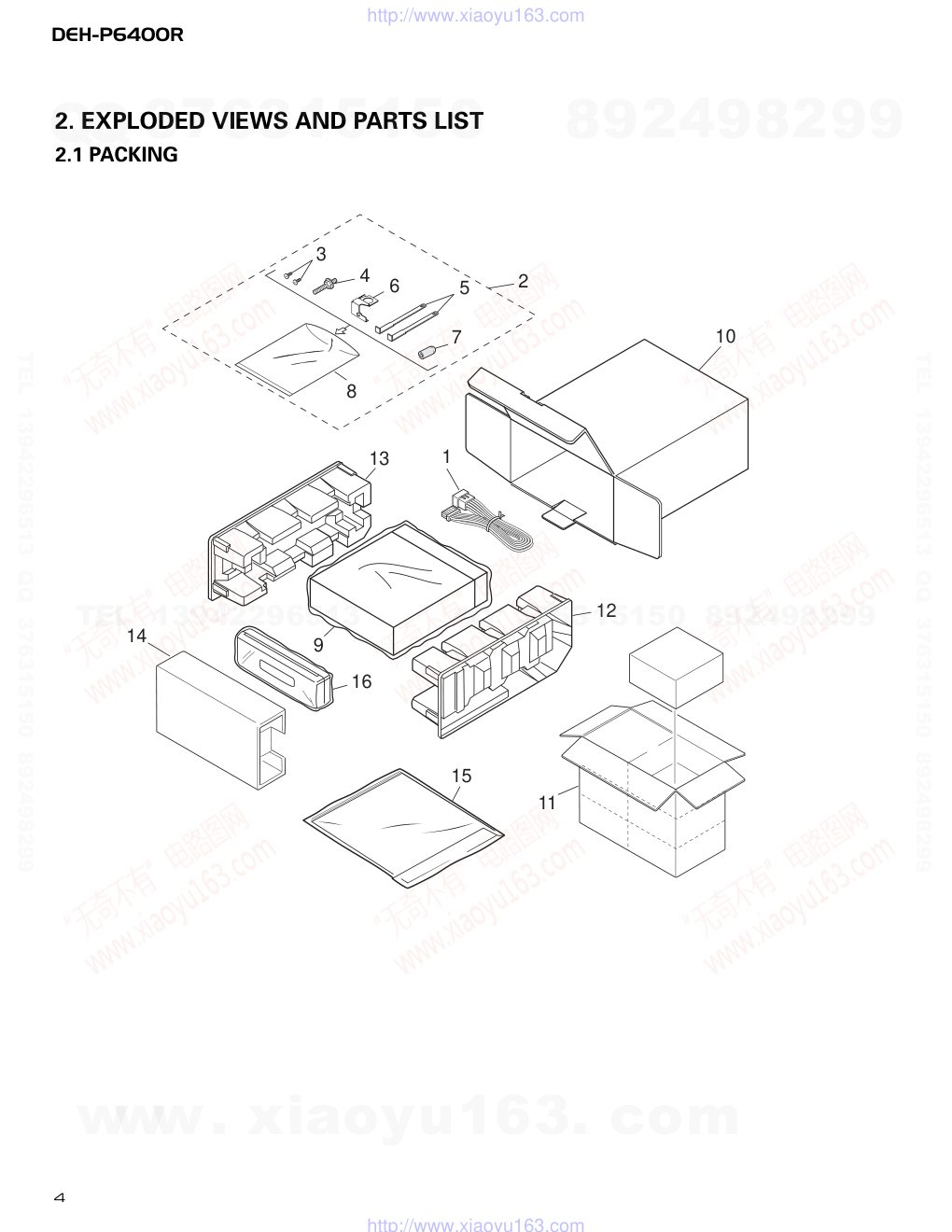
2. EXPLODED VIEWS AND PARTS LIST
2.1 PACKING
10
14
16
13
1
9
12
15
2
7
5
6
4
3
8
11
www. xiaoyu163. com
QQ 376315150
9
9
2
8
9
4
2
9
8
TEL 13942296513
9
9
2
8
9
4
2
9
8
0
5
1
5
1
3
6
7
3
Q
Q
TEL 13942296513 QQ 376315150 892498299
TEL 13942296513 QQ 376315150 892498299
http://www.xiaoyu163.com
5
DEH-P6400R
- Owner's Manual, Installation Manual
Part No.
Language
CRD3513
English, Spanish
CRD3514
German, French
CRB3515
Italian, Dutch
CRD3529
English, Spanish, German, French, Italian, Dutch
1 Cord Assy
CDE6435
2 Accessory Assy
CEA3062
3 Screw
BPZ20P060FZK
4 Screw
CBA1002
5 Handle
CNC5395
6 Earth Plate
CNC9450
7 Bush
CNV3930
*
8 Polyethylene Bag
E36-615
9 Polyethylene Bag
CEG-162
10 Carton
CHG4628
11 Contain Box
CHL46283
12 Protector
CHP2251
13 Protector
CHP2252
14 Inner Box
CHW1754
15-1 Owner’s Manual
CRD3513
15-2 Owner’s Manual
CRD3514
15-3 Owner’s Manual
CRD3515
15-4 Installation Manual
CRD3529
*
15-5 Caution Card
CRP1207
*
15-6 Passport
CRY1013
*
15-7 Warranty Card
CRY1157
15-8 Polyethylene Bag
CEG1116
16 Case Assy
CXB3520
Mark
No. Description
Part No.
Mark
No. Description
Part No.
- PACKING SECTION PARTS LIST
NOTE:
- Parts marked by “*” are generally unavailable because they are not in our Master Spare Parts List.
- Screws adjacent to ∇ mark on the product are used for disassembly.
www. xiaoyu163. com
QQ 376315150
9
9
2
8
9
4
2
9
8
TEL 13942296513
9
9
2
8
9
4
2
9
8
0
5
1
5
1
3
6
7
3
Q
Q
TEL 13942296513 QQ 376315150 892498299
TEL 13942296513 QQ 376315150 892498299
http://www.xiaoyu163.com
6
DEH-P6400R
2.2 EXTERIOR
www. xiaoyu163. com
QQ 376315150
9
9
2
8
9
4
2
9
8
TEL 13942296513
9
9
2
8
9
4
2
9
8
0
5
1
5
1
3
6
7
3
Q
Q
TEL 13942296513 QQ 376315150 892498299
TEL 13942296513 QQ 376315150 892498299
http://www.xiaoyu163.com
DEH-P6400R
1 Screw
BMZ30P040FZK
2 Screw
BMZ30P100FMC
3 Screw
BSZ26P060FMC
4 Screw
BSZ30P040FMC
5 Cord Assy
CDE6435
6 Cap
CKX-003
7 Cord Assy
CDE6717
8 Cable
CDE6714
9 Cord Assy
CDE6454
10 Fuse(10A)
CEK1136
11 Case
CNB2686
12 Holder
CNC5704
13 Holder
CNC8659
14 Cushion
CNM4870
15 Insulator
CNM7214
16 Insulator
CNM7629
17 •••••
18 Tuner Amp Unit
CWM7984
19 Screw
ASZ26P060FMC
20 Screw
BPZ26P120FMC
21 Screw
BSZ26P160FMC
22 Clamper
CEF1007
23 Pin Jack(CN351)
CKB1035
24 Plug(CN901)
CKM1330
25 Plug(CN451)
CKS1049
26 Connector(CN101)
CKS3408
27 Plug(CN801)
CKS3537
28 Connector(CN352)
CKS3598
29 Connector(CN653)
CKS3835
30 Antenna Jack(CN401)
CKX1056
31 Holder
CNC5399
32 Holder
CNC8615
33 Holder
CNC9469
34 Insulator
CNM6949
35 Heat Sink
CNR1583
36 FM/AM Tuner Unit
CWE1562
37 Holder
CNC8815
38 Button(EJECT)
CAC6839
39 Screw(M2x2)
CBA1176
40 Washer
CBF1038
41 Washer
CBF1039
42 Spring
CBH2428
43 Spring
CBH2429
44 Spring
CBL1512
45 Holder
CNC9096
46 Cover
CNM6854
47 Panel
CNS6930
48 Pin
CNV6486
49 Lighting Conductor
CNV6487
50 Gear
CNV6507
51 Arm
CNV6508
52 Panel Unit
CWM7986
53 Socket(CN1850)
CKS3550
54 Connector(CN1851)
CKS4462
55 Damper Unit
CXB5070
56 Holder Unit
CXB6356
57 Holder Unit
CXB6357
58 Clutch Unit
CXB6358
59 Screw
IMS20P045FZK
60 Detach Grille Assy
CXB7914
61 Screw
BPZ20P080FMC
62 Screw
BPZ20P100FZK
63 Button(SELECT)
CAC7220
64 Button(SFEQ)
CAC7221
65 Button(TA)
CAC7223
66 Button(AUDIO)
CAC7224
67 Button(1-6)
CAC7225
68 Button(DISP)
CAC7226
69 Button(OPEN)
CAC7227
70 Button(EQ)
CAC7231
71 Button(FUNC)
CAC7489
72 Spring
CBH2630
73 Spring
CBH2431
74 Spring
CBH2430
75 Spring
CBL1470
76 Cover
CNS6740
77 Holder
CNV6505
78 Holder
CNV6506
79 Holder
CNV6909
80 Keyboard Unit
CWM7990
81 Connector(CN1901)
CKS4524
82 Holder
CNC9642
83 Cushion
CNM6633
84 Cushion
CNM7469
85 Spacer
CNM7697
86 Spacer
CNM7698
87 Holder
CNV6910
88 IC(IC1903)
TSOP1840SB3V
89 OEL Unit
MXS8017
90 Sub Grille Assy
CXB8815
91 IC(IC301)
PAL007A
92 Chassis Unit
CXB8480
93
CD Mechanism Module(S9ANA) CXK5501
94 Screw
ISS26P055FUC
95 Transistor(Q921,999)
2SD2396
*
96 Knob
CAA2697
97 Spacer
CNM7807
98 Cushion
CNM7808
Mark
No. Description
Part No.
Mark
No. Description
Part No.
7
- EXTERIOR SECTION PARTS LIST
www. xiaoyu163. com
QQ 376315150
9
9
2
8
9
4
2
9
8
TEL 13942296513
9
9
2
8
9
4
2
9
8
0
5
1
5
1
3
6
7
3
Q
Q
TEL 13942296513 QQ 376315150 892498299
TEL 13942296513 QQ 376315150 892498299
http://www.xiaoyu163.com
8
DEH-P6400R
2.3 CD MECHANISM MODULE
D
GEM1035
GEM1035
GEM1040
www. xiaoyu163. com
QQ 376315150
9
9
2
8
9
4
2
9
8
TEL 13942296513
9
9
2
8
9
4
2
9
8
0
5
1
5
1
3
6
7
3
Q
Q
TEL 13942296513 QQ 376315150 892498299
TEL 13942296513 QQ 376315150 892498299
http://www.xiaoyu163.com
9
DEH-P6400R
Mark No. Description
Part No.
Mark No. Description
Part No.
1 Control Unit
CWX2481
2 Connector(CN701)
CKS1959
3 Connector(CN101)
CKS3486
4 Screw
BMZ20P025FMC
5 Screw
BSZ20P040FMC
6 Screw(M2x4)
CBA1362
7 Screw(M2x3)
CBA1527
8 Screw
CBA1545
9 Washer
CBF1037
10 Washer
CBF1038
11 Washer
CBF1039
12 Washer
CBF1060
13 Spring
CBH2378
14 Spring
CBH2379
15 Spring
CBH2514
16 Spring
CBH2533
17 Spring
CBH2382
18 Spring
CBH2383
19 Spring
CBH2384
20 Spring
CBH2527
21 Spring
CBH2386
22 Spring
CBH2537
23 Spring
CBH2390
24 Spring
CBH2391
25 Spring
CBH2523
26 Spring
CBH2426
27 Spring
CBH2444
28 Spring
CBL1561
29 Spring
CBL1553
30 Shaft
CLA3845
31 Roller
CLA3910
32 Frame
CNC9654
33 Lever
CNC9664
34 Lever
CNC8949
35 Arm
CNC9661
36 Arm
CNC9016
37 Arm
CNC9017
38 Bracket
CNC9123
39 Frame
CNC9656
40 Belt
CNT1086
41 Gear
CNV6886
42 Gear
CNV6316
43 Gear
CNV6317
44 Gear
CNV6318
45 Gear
CNV6319
46 Gear
CNV6320
47 Arm
CNV6322
48 Arm
CNV6323
49 Arm
CNV6324
50 Arm
CNV6888
51 Arm
CNV6889
52 Guide
CNV6327
53 Arm
CNV6924
54 Guide
CNV6921
55 Rack
CNV6923
56 Clamper
CNV6331
57 Arm
CNV6332
58 Guide
CNV6333
59 Cover
CNV6334
60 Arm
CNV6335
61 Guide
CNV6336
62 Roller
CNV6338
63 Damper
CNV6339
64 Damper
CNV6340
65 Guide
CNV6925
66 Chassis Unit
CXB7980
*
67 Arm Unit
CXB7983
68 Arm Unit
CXB7984
69 Arm Unit
CXB7985
70 Motor Unit(M2)
CXB5903
71 Screw Unit
CXB5904
72 Gear Unit
CXB8076
73 Bracket Unit
CXB7982
74 Motor Unit(M1)
CXB6007
75 Arm Unit
CXB8504
76 Screw(M2x5)
EBA1028
77 Screw
JFZ20P020FMC
78 Screw
JGZ17P020FZK
79 Washer
YE15FUC
80 Washer
YE20FUC
81 Pickup Unit(Service)(P9)
CXX1480
82 Screw
IMS26P030FMC
83 Guide
CNV6922
84 Roller
CNV6887
85 Spring
CBH2509
86 Spring
CBH2512
87 Spring
CBH2536
88 Collar
CNV6906
- CD MECHANISM MODULE SECTION PARTS LIST
www. xiaoyu163. com
QQ 376315150
9
9
2
8
9
4
2
9
8
TEL 13942296513
9
9
2
8
9
4
2
9
8
0
5
1
5
1
3
6
7
3
Q
Q
TEL 13942296513 QQ 376315150 892498299
TEL 13942296513 QQ 376315150 892498299
http://www.xiaoyu163.com
10
DEH-P6400R
A
1
2
3
4
B
C
D
1
2
3
4
3. BLOCK DIAGRAM AND SCHEMATIC DIAGRAM
3.1 BLOCK DIAGRAM
Q153
Q151
Q402
Q155
Q501
IC 501
PM4009A
IC 101
HA12187FP
X501
RDS
DECODER
IP-BUS DRIVER
12
11
20
8
87
MUTE
XOUT
XIN
PEE
24
VDCONT
34
OELPW
22
40
SYSTEM CONTROLLER
IC 601(2/2)
PD5700B
CN401
VDD
VCC
ANT
1
2
BUS-
BU
BUS+
BUS+L
BUS-L
1
2
8
6
5
TX
RX
IPPW
SWVDD
BU
CN653
BU
Q852
Q991
Q999
TUNER AMP UNIT
13
X
15
14
1
24
VDD
SWDACC
T
BUS+L
BUS-L
CD L
Q851
35
DPDT
36
KYDT
23
SYSPW
Q101
Q102
IC 851
NJM2360
6
EJTIN
44
CONT
CD5VON
HOME
CDLOEJ
DSCSNS
58
68
69
65
89
43
ILMPW
41
DSENS
TEL
FUSE
200mA
2
1
CN451
TEL
CN701
CN101
94
LVLINL
L
TC7SET0
IC 801
4
A
D
5
8
1
7
CN101
11
BUZZER
IC 3
EEPROM
FM/AM TUNER UNIT
28
27
FM/AM 1ST IF 10.7MHz
T51 Q51 CF51
CF52 CF53
IC1
MIXER, IF AMP, DET.
6
21
18
LDET
COMP
22
25
10
14
12
15 16
8
13
2
3
4
CF202
VDD
VCC
DI/DO
CE2
CK
CE1
SDBW
SL
FMSD
NL1
NL2
IC 2 FM MPX
AMANT
FMANT
ATT
ATT
AMRF
FMRF
RF ADJ
ANT2 ADJ
X901
10.25MHz
ANT1 ADJ
LOCL
23
LOCH
AMDET
MPXREF 41kHz
AM 2ND IF
450kHz
19
CREQ
11
DGND
1
STIND
L ch
5
R ch
9
24
NC
FMLOCL
20
17
7
NC
NC
WC
26 RFGND
Q101
M
LASER
DIODE
MONITOR
DIODE
CLAMP
SENSE
DISC
SENSE
FOCUS ACT.
SPINDLE
MOTOR
M
CARRIAGE
MOTOR
LOAD/
TRACKING ACT.
LD-
MD
FO+
TO+
15
5
4
1
PICKUP UNIT(SERVICE)(P9)
HOLOGRAM
UNIT
IC 401
BA5996FM
IC 201
TC9495F2
IC 701
BA05SFP
+5V REGULATOR
SERVO
CONTROL,
DSP,
LPF, DAC
CD
DRIVER
17
DSCSNS
2
VD
VD
VDD
11
CONT
10
LOEJ
14
L-OUT
1
CD5VON
TOP
FOP
16
SOP
15
SOM
17
LCOP
18
LCOM
22
1
2
LOEJ
78
85
L_OUT
79
9
MUTE
12
FOP
TD/FD
AC,BD
F,E
SD/MD
38
RFI
43
FEI
4
14
TOP
S901
HOME
12EJ
SENSE
8EJ
SENSE
HOME
16
LD+
14
VDD
9
LDO
8
MDI
IC 101
TA2153FN
RFRPIN
FEO
TEO
24
16
14
46
TEI
RF-AMP
17
2
11
10
14
1
16
CONTROL UNIT
www. xiaoyu163. com
QQ 376315150
9
9
2
8
9
4
2
9
8
TEL 13942296513
9
9
2
8
9
4
2
9
8
0
5
1
5
1
3
6
7
3
Q
Q
TEL 13942296513 QQ 376315150 892498299
TEL 13942296513 QQ 376315150 892498299
http://www.xiaoyu163.com
DEH-P6400R
5
6
7
8
A
B
C
D
5
6
7
8
11
19
LDET
48
FM/AM
52
12
1
TMUTE
BSENS
ASENS
NL2DT
VDD
BU
74
73
SD
SL
TUNPCE
TUNPCK
TUNPCE2
TUNPDO
ASENBO
10
FL
11
RL
87
MUTE
XOUT
XIN
ILB
SWVDD
OELB
ILB
SWDVDD
OELB
23
21
3
5
FL-
FL+
RL-
RL+
ACC
51
50
97
IN3-L
42
IN4+L
43
IN4-L
44
IN2-L
41
72
2
71
1
82
30 29 81
FLIN
14
RLIN
12
22
4
RESET
POWER AMP
IC 601(1/2)
PD5700B
ER
IC 203
PML008A
IC 961
S-80735ANDZI
IC 301
PAL007A
RESET
VDD
Q911
Q931
SYSPW
BU
TX
RX
TX
RX
IPPW
ELECTRONIC VOLUME/
SOURCE SELECTOR
BU
BU
STBY
MUTE
IC 1901
PD5706A
OEL CONTROLLER/
KEY CONTROLLER
KEY MATRIX
9
11
8
KEY DATA
OEL DATA
VDD
14
CN801
CN1901
Q803
Q804
Q802
13
X601
15
2
ACC
VST,VCK,VDT
TUN L
BUS+L
BUS-L
CD L
DPDT
3
5
DPDT
KYDT
SYS+B
BU
Q921
Q922
23
YSPW
BU
Q301
MUTE
Q351
FL
5
Q353
FL
R L
Q801
IC 851
NJM2360M
6
1
EJTIN
44
7
2
10
11
14
8
7
2
10
11
14
8
CN1850
CN1851
S1850
KYDT
4
2
5
10
8
IC 1902
PD8088A
FONT ROM
IC 1903
TSOP1840SB3V
REMOTE CONTROL SENSOR
OPT IN
3
1
5
GREEN
REM
27
28
DPDT
KTDT
EJECT
OEL UNIT
Q1941
4,16
2,8
MUTE
FL
RL
IC 631
PDH0045A
S801
DSENS
SYSTEM CONTROLLER
Q932
Q951
VDD
ISENS
83
TELIN
10
25
B.REMOTE
FL-
FL+
RL-
RL+
TEL
40
IN1-L
IC 1904
S-818A33AUC-BGN
3.3V REGULATOR
1
5
VDD REGULATOR
ILL SENSE
BACKUP SENSE
ACC SENSE
TELEPHONE MUTE
SYS+B REGULATOR
3
9
11
12
10
2
5
8
6
3
9
11
12
10
2
5
8
6
1
1
NJM4558MD
IC 132
5
7
94
VLINL
1
SEL_OUT_L
LEVEL INDICATOR
TC7SET08FU
IC 801
2
4
PANEL UNIT
B
KEYBOARD UNIT
C
CN901
Q982
B.U
CN351
CN352-2
NL1
SDBW
95
53
BACK UP
GND
RR
+
RR
-
FR
+
FR
-
FL
+
FL
-
RL
+
RL
-
ACC
GND
BACK
UP
B.
REM
FUSE
10A
ACC
ILL
TELMUTE
B.REM
ILL
www. xiaoyu163. com
QQ 376315150
9
9
2
8
9
4
2
9
8
TEL 13942296513
9
9
2
8
9
4
2
9
8
0
5
1
5
1
3
6
7
3
Q
Q
TEL 13942296513 QQ 376315150 892498299
TEL 13942296513 QQ 376315150 892498299
http://www.xiaoyu163.com
12
DEH-P6400R
A
1
2
3
4
B
C
D
1
2
3
4
3.2 OVERALL CONNECTION DIAGRAM(GUIDE PAGE)
Note: When ordering service parts, be sure to refer to “EXPLODED VIEWS AND PARTS LIST” or “ELECTRICAL PARTS
LIST”.
A-a
A-b
A-a
A-b
A-b
A-a
Large size
SCH diagram
Guide page
Detailed page
A
A-a A-b
A-a A-b
A-a
A-
CN451
2
3
1
4
EJECT
PDH0045A
1K
47K
100K
11
10
9
8
7
6
5
4
3
2
1
Decimal points for resistor
and capacitor fixed values
are expressed as :
2.2 2R2
0.022 R022
←
←
The > mark found on some component parts indicates
the importance of the safety factor of the part.
Therefore, when replacing, be sure to use parts of
identical designation.
Symbol indicates a resistor.
No differentiation is made between chip resistors and
discrete resistors.
NOTE :
Symbol indicates a capacitor.
No differentiation is made between chip capacitors and
discrete capacitors.
>
PANEL UNIT
KEYBOARD UNIT
CN1901
FM/AM TUNER UNIT
CN701
IP-BUS
IP-BUS
DRIVER
HANDSFREE
RDS DECODER
SYST
TEL
ANTENNA
JACK
CONTROL UNIT
VD REGULATOR
B
C
D
FM(100%):-15.5dBs
AM(30%):-26.0dBs
CD:-0.2dBs
IP-BUS:+2.2dBs
FM: -16.5
AM: -27.0
IP-BUS: +2.2
CD: -0.2
CD5VON
VD
XRST
XCE
XPCE
XPIO0
XPIO1
XPIO2
XPIO3
CDLOAJ
CONT
Rch
AGND
Lch
CLCONT
HOME
DSCSNC
GND
GND
PGND
PGND
NC
NC
NC
NC
NC
NC
NC
CONT
XPIO1
XPIO2
XPIO3
XPIO0
VDCONT
100K
A-a
B
www. xiaoyu163. com
QQ 376315150
9
9
2
8
9
4
2
9
8
TEL 13942296513
9
9
2
8
9
4
2
9
8
0
5
1
5
1
3
6
7
3
Q
Q
TEL 13942296513 QQ 376315150 892498299
TEL 13942296513 QQ 376315150 892498299
http://www.xiaoyu163.com
13
DEH-P6400R
5
6
7
8
A
B
C
D
5
6
7
8A
b
600µH
100K
1
2
4
3
2
1
4
3
6
5
8
7
10
9
12
11
14
13
16
15
RR
+
RR
-
FR
+
FR
-
FL
+
FL
-
RL
+
RL
-
ACC
GND
B.
REM
BACK
UP
RR+
RR-
FR+
FR-
FL+
FL-
RL+
RL-
ACC
GND
B.REM
BACK UP
TEL MUTE
2
1
4
3
6
5
8
7
10
9
12
11
14
13
16
15
ILL
ILL
FUSE 10A
CEK1136
HTELM
EMUTE
1R5K
1R5K
PAL007A
0R0
0R0
REAR
R CH
REAR
L CH
FRONT
L CH
FRONT
R CH
TUNER AMP UNIT
ELECTRONIC VOLUME,
SOURCE SELECTOR
TEM CONTROLLER
RESET
LEVEL INDICATOR
MUTE
MUTE
POWER AMP
DC/DC CONVERTER
TEL
BSENSE
ASENSE
ILL SENSE
>
PML008A
MUTE
MUTE
VDD REGULATOR
SYS+B REGULATOR
A
5dBs
0dBs
2dBs
2dBs
FM: +6.6dBs
AM: -1.9dBs
IP-BUS: +9.3dBs
CD: +9.9dBs
FM:+5.84dBs
AM: -2.66dBs
IP-BUS:+8.54dBs
CD:+9.14dBs
FM: +36.2dBs
AM: +24.1dBs
IP-BUS: +35.3dBs
CD: +35.9dBs
XPIO0
CDLOEJ
CLCONT
NC
CD5VON
XPCK
XCE
XRST
TEMP
HOME
A-b
www. xiaoyu163. com
QQ 376315150
9
9
2
8
9
4
2
9
8
TEL 13942296513
9
9
2
8
9
4
2
9
8
0
5
1
5
1
3
6
7
3
Q
Q
TEL 13942296513 QQ 376315150 892498299
TEL 13942296513 QQ 376315150 892498299
http://www.xiaoyu163.com
14
DEH-P6400R
A
1
2
3
4
B
C
D
1
2
3
4
A-a A-b
A-a A-b
A-a A-b
A-a
A-b
CN451
PDH0045A
1K
47K
100K
11
10
9
8
7
6
5
4
3
2
1
Decimal points for resistor
and capacitor fixed values
are expressed as :
2.2 2R2
0.022 R022
←
←
The > mark found on some component parts indicates
the importance of the safety factor of the part.
Therefore, when replacing, be sure to use parts of
identical designation.
Symbol indicates a resistor.
No differentiation is made between chip resistors and
discrete resistors.
NOTE :
Symbol indicates a capacitor.
No differentiation is made between chip capacitors and
discrete capacitors.
>
CN701
IP-BUS
IP-BUS
DRIVER
HANDSFREE
TEL
CONTROL UNIT
VD REGULATOR
D
M(100%):-15.5dBs
M(30%):-26.0dBs
CD:-0.2dBs
IP-BUS:+2.2dBs
FM: -16.5dBs
AM: -27.0dBs
IP-BUS: +2.2dBs
CD: -0.2dBs
CD5VON
VD
XRST
XCE
XPCE
XPIO0
XPIO1
XPIO2
XPIO3
CDLOAJ
CONT
Rch
AGND
Lch
CLCONT
HOME
DSCSNC
GND
GND
PGND
PGND
1
A-a
www. xiaoyu163. com
QQ 376315150
9
9
2
8
9
4
2
9
8
TEL 13942296513
9
9
2
8
9
4
2
9
8
0
5
1
5
1
3
6
7
3
Q
Q
TEL 13942296513 QQ 376315150 892498299
TEL 13942296513 QQ 376315150 892498299
http://www.xiaoyu163.com
15
DEH-P6400R
5
6
7
8
A
B
C
D
5
6
7
8
A-a A-b
2
3
1
4
EJECT
47K
PANEL UNIT
KEYBOARD UNIT
CN1901
FM/AM TUNER UNIT
RDS DECODER
SYSTEM CONTR
ANTENNA
JACK
B
C
FM(100%):-1
AM(30%):-2
NC
NC
NC
NC
NC
NC
NC
CONT
XPIO1
XPIO2
XPIO3
XPIO0
CDLOEJ
CLCONT
NC
VDCONT
100K
2
3
4
A-a B
www. xiaoyu163. com
QQ 376315150
9
9
2
8
9
4
2
9
8
TEL 13942296513
9
9
2
8
9
4
2
9
8
0
5
1
5
1
3
6
7
3
Q
Q
TEL 13942296513 QQ 376315150 892498299
TEL 13942296513 QQ 376315150 892498299
http://www.xiaoyu163.com
16
DEH-P6400R
A
1
2
3
4
B
C
D
1
2
3
4
A-a A-b
A-b
1
2
4
3
PAL007A
0R0
0R0
REAR
R CH
REAR
L CH
FRONT
L CH
FRONT
R CH
TUNER AMP UNIT
ELECTRONIC VOLUME,
SOURCE SELECTOR
RESET
LEVEL INDICATOR
MUTE
POWER AMP
PML008A
MUTE
MUTE
A
5dBs
0dBs
2dBs
2dBs
FM: +6.6dBs
AM: -1.9dBs
IP-BUS: +9.3dBs
CD: +9.9dBs
FM:+5.84dBs
AM: -2.66dBs
IP-BUS:+8.54dBs
CD:+9.14dBs
1
www. xiaoyu163. com
QQ 376315150
9
9
2
8
9
4
2
9
8
TEL 13942296513
9
9
2
8
9
4
2
9
8
0
5
1
5
1
3
6
7
3
Q
Q
TEL 13942296513 QQ 376315150 892498299
TEL 13942296513 QQ 376315150 892498299
http://www.xiaoyu163.com
17
DEH-P6400R
5
6
7
8
A
B
C
D
5
6
7
8
A-b
A-a A-b
b
600µH
100K
2
1
4
3
6
5
8
7
10
9
12
11
14
13
16
15
RR
+
RR
-
FR
+
FR
-
FL
+
FL
-
RL
+
RL
-
ACC
GND
B.
REM
BACK
UP
RR+
RR-
FR+
FR-
FL+
FL-
RL+
RL-
ACC
GND
B.REM
BACK UP
TEL MUTE
2
1
4
3
6
5
8
7
10
9
12
11
14
13
16
15
ILL
ILL
FUSE 10A
CEK1136
HTELM
EMUTE
1R5K
1R5K
EM CONTROLLER
MUTE
DC/DC CONVERTER
TEL
BSENSE
ASENSE
ILL SENSE
>
VDD REGULATOR
SYS+B REGULATOR
FM: +36.2dBs
AM: +24.1dBs
IP-BUS: +35.3dBs
CD: +35.9dBs
XPIO0
CDLOEJ
CLCONT
NC
CD5VON
XPCK
XCE
XRST
TEMP
HOME
2
3
4
www. xiaoyu163. com
QQ 376315150
9
9
2
8
9
4
2
9
8
TEL 13942296513
9
9
2
8
9
4
2
9
8
0
5
1
5
1
3
6
7
3
Q
Q
TEL 13942296513 QQ 376315150 892498299
TEL 13942296513 QQ 376315150 892498299
http://www.xiaoyu163.com
18
DEH-P6400R
A
1
2
3
4
B
C
D
1
2
3
4
3.3 KEYBOARD UNIT
REMOTE CONTROL
SENSOR
3.3V REGULATOR
DISP/SCRL
ENT
SFEQ
←
←
←
←
BAND/ESC
VOLUME
TA
TEXT
CL170PGCD
CL170PGCD
C
B
CN1851
1
2
3
6
5
4
1
2
3
6
5
4
1
2
3
6
5
4
1
2
3
6
5
4
1
2
3
6
5
4
1
2
3
6
5
4
1
2
3
6
5
4
1
2
3
6
5
4
1
2
3
6
5
4
1
2
3
6
5
4
1
2
3
6
5
4
1
2
3
6
5
4
1
2
3
6
5
4
1
2
3
6
5
4
1
2
3
6
5
4
1
2
3
6
5
4
1
2
3
6
5
4
1
2
3
6
5
4
C
www. xiaoyu163. com
QQ 376315150
9
9
2
8
9
4
2
9
8
TEL 13942296513
9
9
2
8
9
4
2
9
8
0
5
1
5
1
3
6
7
3
Q
Q
TEL 13942296513 QQ 376315150 892498299
TEL 13942296513 QQ 376315150 892498299
http://www.xiaoyu163.com
DEH-P6400R
5
6
7
8
A
B
C
D
5
6
7
8
19
KEY CONTROL AND OEL CONTROL
FONT ROM
OEL UNIT MXS8017
C
C KEYBOARD UNIT
C
www. xiaoyu163. com
QQ 376315150
9
9
2
8
9
4
2
9
8
TEL 13942296513
9
9
2
8
9
4
2
9
8
0
5
1
5
1
3
6
7
3
Q
Q
TEL 13942296513 QQ 376315150 892498299
TEL 13942296513 QQ 376315150 892498299
http://www.xiaoyu163.com
20
DEH-P6400R
A
1
2
3
4
B
C
D
1
2
3
4
M1 CXB6007
M2 CXB5903
LOADING/CARRIAGE
SPINDLE
RF AMP
ACT/MOTOR DRIVER
5V REGULATOR
CN101
3.4 CD MECHANISM MODULE
D
D
CONTROL UNIT
PICKUP UNIT(SERVICE)(P9)
www. xiaoyu163. com
QQ 376315150
9
9
2
8
9
4
2
9
8
TEL 13942296513
9
9
2
8
9
4
2
9
8
0
5
1
5
1
3
6
7
3
Q
Q
TEL 13942296513 QQ 376315150 892498299
TEL 13942296513 QQ 376315150 892498299
http://www.xiaoyu163.com
21
DEH-P6400R
5
6
7
8
A
B
C
D
5
6
7
8
16.934MHz
SERVO CONTROL/DSP/DAC/LPF
R
CN701
TC9495F2
SWITCHES:
CONTROL UNIT
S901 : HOME SWITCH.....ON-OFF
S902 : CLAMP SWITCH....ON-OFF
S903 : DSCSNS SWITCH....ON-OFF
S904 : 12EJ SWITCH....ON-OFF
S905 : 8EJ SWITCH....ON-OFF
The underlined indicates the switch position.
A
CN653
D
www. xiaoyu163. com
QQ 376315150
9
9
2
8
9
4
2
9
8
TEL 13942296513
9
9
2
8
9
4
2
9
8
0
5
1
5
1
3
6
7
3
Q
Q
TEL 13942296513 QQ 376315150 892498299
TEL 13942296513 QQ 376315150 892498299
http://www.xiaoyu163.com
22
DEH-P6400R
@ CH1:BCK
2V/div.
During "Play"
1 CH1:DSCSNS
5V/div.
2 CH2:CLCONT
5V/div.
3 CH3:LOEJ
5V/div.
4 CH4:VD
10V/div.
When loading (8 cm CD)
500ms/div.
5 CH1:FD
500mV/div.
6 CH2:FOK
5V/div.
7 CH3:MD
5V/div.
When setting up "Source On"
500ms/div.
8 CH1:FE
500mV/div.
9 CH2:FOON 5V/div.
When setting up "Source On"
500ms/div.
5 CH1:FD
500mV/div.
6 CH2:FOK
5V/div.
7 CH3:MD
5V/div.
Magnified drawing for "time"
100ms/div.
1 CH1:DSCSNS
5V/div.
2 CH2:CLCONT
5V/div.
3 CH3:LOEJ
5V/div.
4 CH4:VD
10V/div.
When loading (12 cm CD)
Ref. :
GND
Mode :
Normal
Ref. :
GND
Mode :
Normal
Ref. :
VREF
Mode :
Normal
Ref. :
VREF
Mode :
Normal
Ref. :
VREF
Mode :
Normal
Ref. :
VREF
Mode :
Normal
Ref. :
VREF
Mode :
Normal
Ref. :
VREF
Mode :
Normal
Ref. :
VREF
Mode :
Normal
Ref. :
VREF
Mode :
Test
Ref. :
VREF
Mode :
Normal
Ref. :
VREF
Mode :
Normal
500ms/div.
0 CH1:TE
500mV/div.
8 CH2:FE
500mV/div.
When setting up "Source On"
200ms/div.
1µs/div.
# CH1:LRCK
2V/div.
$ CH2:DOUT 2V/div.
During "Play"
10µs/div.
7 CH1:MD
500mV/div.
During "Play"
10µs/div.
% CH1:RFO
500mV/div.
During "Play"
0.5µs/div.
% CH1:RFO
500mV/div.
0 CH2:TE
500mV/div.
During "Tracking Open"
2ms/div.
8 CH1:FE
500mV/div.
5 CH2:FD
500mV/div.
0 CH3:TE
500mV/div.
! CH4:TD
500mV/div.
During "Play"
1ms/div.
- Waveforms
Note:1. The encircled numbers denote measuring pointes in the circuit diagram.
2. Reference voltage
VREF:2.1V
www. xiaoyu163. com
QQ 376315150
9
9
2
8
9
4
2
9
8
TEL 13942296513
9
9
2
8
9
4
2
9
8
0
5
1
5
1
3
6
7
3
Q
Q
TEL 13942296513 QQ 376315150 892498299
TEL 13942296513 QQ 376315150 892498299
http://www.xiaoyu163.com
23
DEH-P6400R
% CH1:RFO
1V/div.
0 CH2:TE
500mV/div.
& CH3:DFCT
5V/div.
During inside/outside search
200ms/div.
% CH1:RFO
1V/div.
0 CH2:TE
500mV/div.
! CH3:TD
1V/div.
1 Track Jump
500µs/div.
% CH1:RFO
1V/div.
0 CH2:TE
1V/div.
! CH3:TD
1V/div.
100 Track Jump
5ms/div.
% CH1:RFO
1V/div.
0 CH2:TE
1V/div.
! CH3:TD
1V/div.
32 Track Jump
5ms/div.
5 CH1:FD
1V/div.
^ CH2:FOP
2V/div.
With no disk inserted
During "Focus Close"
200ms/div.
1 CH1:DSCSNS
5V/div.
2 CH2:CLCONT
5V/div.
3 CH3:LOEJ
5V/div.
When "Eject" (8cm CD)
200ms/div.
* CH1:TEY
500mV/div.
( CH2:SD
2V/div.
During inside/outside search
200ms/div.
1 CH1:DSCSNS
5V/div.
2 CH2:CLCONT
5V/div.
3 CH3:LOEJ
5V/div.
When "Eject" (12 cm CD)
200ms/div.
% CH1:RFO
2V/div.
& CH2:DFCT
5V/div.
5 CH3:FD
1V/div.
! CH4:TD
2V/div.
When reproducing black dots (800µm)
500µs/div.
Ref. :
VREF
Mode :
Test
Ref. :
VREF
Mode :
Test
Ref. :
VREF
Mode :
Normal
Ref. :
VREF
Mode :
Normal
Ref. :
VREF
Mode :
Test
Ref. :
VREF
Mode :
Test
Ref. :
VREF
Mode :
Normal
Ref. :
GND
Mode :
Normal
Ref. :
GND
Mode :
Normal
) CH1:LOUT
2V/div.
⁄ CH2:ROUT 2V/div.
"Play" in 1kHz, 0dB
200µs/div.
Ref. :
GND
Mode :
Normal
www. xiaoyu163. com
QQ 376315150
9
9
2
8
9
4
2
9
8
TEL 13942296513
9
9
2
8
9
4
2
9
8
0
5
1
5
1
3
6
7
3
Q
Q
TEL 13942296513 QQ 376315150 892498299
TEL 13942296513 QQ 376315150 892498299
http://www.xiaoyu163.com
24
DEH-P6400R
A
1
2
3
4
B
C
D
1
2
3
4
A
Capacitor
Connector
P.C.Board
Chip Part
SIDE A
SIDE B
2
3
4
5
6
7
8
9
10
11
12
13
14
1
15
16
8
7
6
5
4
3
2
1
2
1
DSENS
A TUNER AMP UNIT
CORD ASSY
(OUTPUT,POWER
SUPPLY)
CORD ASSY
(PREOUT)
4. PCB CONNECTION DIAGRAM
4.1 TUNER AMP UNIT
NOTE FOR PCB DIAGRAMS
1. The parts mounted on this PCB
include all necessary parts for
several destination.
For further information for
respective destinations, be sure
to check with the schematic dia-
gram.
2. Viewpoint of PCB diagrams
www. xiaoyu163. com
QQ 376315150
9
9
2
8
9
4
2
9
8
TEL 13942296513
9
9
2
8
9
4
2
9
8
0
5
1
5
1
3
6
7
3
Q
Q
TEL 13942296513 QQ 376315150 892498299
TEL 13942296513 QQ 376315150 892498299
http://www.xiaoyu163.com
DEH-P6400R
5
6
7
8
A
B
C
D
5
6
7
8
25
A
IC,Q
3
5
7
9
11 13
1
4
6
8
10 12 14
2
17 19 21 23 25
15
18 20 22 24
16
3
2
1
4
6
5
7 10
9
8
11
3
5
7
9
11
13
1
4
6
8
10
12
14
2
19 17 15 13 11
9
21
5
3
1
7
18 16 14 12 10
8
20
4
2
6
3
5
7
9
11
13
1
17
19
15
4
6
8
10
12
14
2
18
20
16
28
ANTENNA
JACK
1
3
4
2
RL
RR
PRE OUT
IP-BUS
B CN1850
FRONT
FM/AM TUNER UNIT
CORD ASSY
(TEL)
D CN701
SIDE A
www. xiaoyu163. com
QQ 376315150
9
9
2
8
9
4
2
9
8
TEL 13942296513
9
9
2
8
9
4
2
9
8
0
5
1
5
1
3
6
7
3
Q
Q
TEL 13942296513 QQ 376315150 892498299
TEL 13942296513 QQ 376315150 892498299
http://www.xiaoyu163.com
26
DEH-P6400R
A
1
2
3
4
B
C
D
1
2
3
4
A
IC,Q
A TUNER AMP UNIT
www. xiaoyu163. com
QQ 376315150
9
9
2
8
9
4
2
9
8
TEL 13942296513
9
9
2
8
9
4
2
9
8
0
5
1
5
1
3
6
7
3
Q
Q
TEL 13942296513 QQ 376315150 892498299
TEL 13942296513 QQ 376315150 892498299
http://www.xiaoyu163.com
DEH-P6400R
5
6
7
8
A
B
C
D
5
6
7
8
27
2
3
4
1
7
6
5
8
SIDE B
A
www. xiaoyu163. com
QQ 376315150
9
9
2
8
9
4
2
9
8
TEL 13942296513
9
9
2
8
9
4
2
9
8
0
5
1
5
1
3
6
7
3
Q
Q
TEL 13942296513 QQ 376315150 892498299
TEL 13942296513 QQ 376315150 892498299
http://www.xiaoyu163.com
28
DEH-P6400R
A
1
2
3
4
B
C
D
1
2
3
4
1
3
2
4
5 7
6 8
9 11
10 12
B PANEL UNIT
B PANEL UNIT
A
CN801
C
CN1901
EJECT
4.2 PANEL UNIT
B
SIDE B
SIDE A
www. xiaoyu163. com
QQ 376315150
9
9
2
8
9
4
2
9
8
TEL 13942296513
9
9
2
8
9
4
2
9
8
0
5
1
5
1
3
6
7
3
Q
Q
TEL 13942296513 QQ 376315150 892498299
TEL 13942296513 QQ 376315150 892498299
http://www.xiaoyu163.com
29
DEH-P6400R
1
2
3
4
A
B
C
D
1
2
3
4
IC,Q
IC,Q
C
1
5
9
1
2
3
4
5
6
1
2
3
4
5
6
1
2
3
4
5
6
1
2
3
4
5
6
1
2
3
4
5
6
1
2
3
4
5
6
1
2
3
4
5
6
1
2
3
4
5
6
1
2
3
4
5
6
1
2
3
4
5
6
1
2
3
4
5
6
1
2
3
4
5
6
1
2
3
4
5
6
1
2
3
4
5
6
1
2
3
4
5
6
1
2
3
4
5
6
1
2
3
4
5
6
1
2
3
4
5
6
1
2
3
5
6
←
←
←
←
AUDIO
BAND/ESC
SFEQ
6
5
4
3
2
1
SOURCE
VOLUME
TA
EQ
B
CN1851
FUNC
C KEYBOARD UNIT
C KEYBOARD UNIT
DISP/SCRL
1
3
5
6
4
2
12
10
8
11
9
7
5
4
1
3
2
OEL UNIT
OEL UNIT
ADJ
ENT
SELECT
TEXT
TP1
TP2
4.3 KEYBOARD UNIT
SIDE A
SIDE B
C
www. xiaoyu163. com
QQ 376315150
9
9
2
8
9
4
2
9
8
TEL 13942296513
9
9
2
8
9
4
2
9
8
0
5
1
5
1
3
6
7
3
Q
Q
TEL 13942296513 QQ 376315150 892498299
TEL 13942296513 QQ 376315150 892498299
http://www.xiaoyu163.com
30
DEH-P6400R
A
1
2
3
4
B
C
D
1
2
3
4
12EJ
DSCSNS
HOME
4.4 CD MECHANISM MODULE
CONTROL UNIT
SIDE A
D
D
M2 LOADING/CARRIAGE MOTOR
M1 SPINDLE MOTOR
PICKUP UNIT(SERVICE)(P9)
CN653
A
www. xiaoyu163. com
QQ 376315150
9
9
2
8
9
4
2
9
8
TEL 13942296513
9
9
2
8
9
4
2
9
8
0
5
1
5
1
3
6
7
3
Q
Q
TEL 13942296513 QQ 376315150 892498299
TEL 13942296513 QQ 376315150 892498299
http://www.xiaoyu163.com
31
DEH-P6400R
1
2
3
4
A
B
C
D
1
2
3
4
CLAMP
8EJ
SIDE B
CONTROL UNIT
D
D
www. xiaoyu163. com
QQ 376315150
9
9
2
8
9
4
2
9
8
TEL 13942296513
9
9
2
8
9
4
2
9
8
0
5
1
5
1
3
6
7
3
Q
Q
TEL 13942296513 QQ 376315150 892498299
TEL 13942296513 QQ 376315150 892498299
http://www.xiaoyu163.com
DEH-P6400R
5. ELECTRICAL PARTS LIST
NOTES:
- Parts whose parts numbers are omitted are subject to being not supplied.
- The part numbers shown below indicate chip components.
Chip Resistor
RS1/_S___J,RS1/__S___J
Chip Capacitor (except for CQS.....)
CKS....., CCS....., CSZS.....
=====Circuit Symbol and No.===Part Name
Part No.
---
------
------------------------------------------
-------------------------
Unit Number : CWM7984
Unit Name
: Tuner Amp Unit
MISCELLANEOUS
IC
101
IC
HA12187FP
IC
132
IC
NJM4558MD
IC
203
IC
PML008A
IC
301
IC
PAL007A
IC
501
IC
PM4009A
IC
601
IC
PD5700B
IC
631
IC
PDH0045A
IC
801
IC
TC7SET08FU
IC
851
IC
NJM2360M
IC
961
IC
S-80735ANDZI
Q
101
Transistor
2SA1037K
Q
102
Transistor
DTC124EK
Q
151
Transistor
2SD1757K
Q
152
Transistor
2SD1757K
Q
153
Transistor
IMH3A
Q
155
Transistor
2SC2412K
Q
301
Transistor
DTC124EK
Q
351
Transistor
IMH3A
Q
353
Transistor
IMH3A
Q
401
Transistor
2SC2412K
Q
402
Transistor
2SC2412K
Q
501
Transistor
DTA124EK
Q
801
Transistor
IMD2A
Q
802
Transistor
2SD1760F5
Q
803
Transistor
2SD1767
Q
804
Transistor
IMD2A
Q
805
Transistor
DTC143EK
Q
851
Transistor
2SD1760F5
Q
852
Transistor
IMD2A
Q
911
Transistor
2SD1760F5
Q
913
Transistor
IMD2A
Q
921
Transistor
2SD2396
Q
922
Transistor
DTC114EK
Q
923
Transistor
2SB1238
Q
931
Transistor
IMX1
Q
932
Transistor
2SC2412K
Q
951
Transistor
2SA1037K
Q
981
Transistor
2SC2412K
Q
982
Transistor
IMD2A
Q
991
Transistor
IMD2A
Q
999
Transistor
2SD2396
D
131
Diode Network
DA204U
D
132
Diode Network
DA204U
D
133
Diode
DAN202U
D
134
Diode
DAP202U
D
801
Diode
HZS6L(B1)
D
803
Diode Network
DA204U
D
804
Diode
DAN202U
D
805
Diode
DAP202U
D
806
Diode
DAN202U
D
807
Diode
DAP202U
D
808
Diode
HZS11L(A1)
D
851
Diode
HZS9L(C3)
D
852
Diode
RB411D
D
901
Diode
1SR139-400
D
902
Diode
1SR139-400
D
903
Diode
1SR139-400
D
904
Diode
1SR139-400
D
911
Diode
1SR139-400
D
912
Diode
HZS6L(B1)
D
921
Diode
HZS9L(C1)
D
931
Diode
HZS7L(A1)
D
932
Diode
HZS7L(C3)
D
951
Diode
DAN202U
D
981
Diode
DAN202U
D
982
Diode
HZS9L(A2)
D
991
Diode
HZS9L(B1)
ZNR 451
Surge Protector
DSP-201M-A21F
L
171
Inductor
CTF1530
L
401
Ferri-Inductor
LAU2R2K
L
402
Ferri-Inductor
LAU4R7K
L
403
Inductor
LAU1R0K
L
451
Inductor
CTF1378
L
501
Ferri-Inductor
LAU101K
L
502
Ferri-Inductor
LAU2R2K
L
503
Inductor
CTF1378
L
601
Ferri-Inductor
LAU2R2K
L
801
Inductor
LAU100K
L
802
Ferri-Inductor
LAU2R2K
L
852
Inductor
CTF1510
L
853
Inductor
CTF1489
L
901
Choke Coil 600µH
CTH1221
L
951
Ferri-Inductor
LAU2R2K
X
501
Crystal Resonator 3.648MHz
CSS1447
X
601
Radiator 10.00MHz
CSS1475
S
801
Switch(DSENS)
CSN1039
FU
451
Fuse 200mA
CEK1189
FM/AM Tuner Unit
CWE1562
BZ
641
Buzzer
CPV1050
RESISTORS
R
101
RS1/16S101J
R
102
RS1/16S470J
R
103
RS1/16S101J
R
104
RS1/16S222J
R
105
RS1/16S103J
R
106
RS1/16S562J
R
107
RS1/16S332J
R
108
RS1/16S150J
R
109
RS1/16S181J
R
110
RS1/16S181J
R
111
RS1/16S223J
R
112
RS1/16S223J
R
113
RS1/16S102J
R
114
RS1/16S102J
R
143
RS1/16S104J
=====Circuit Symbol and No.===Part Name
Part No.
---
------
------------------------------------------
-------------------------
A
32
www. xiaoyu163. com
QQ 376315150
9
9
2
8
9
4
2
9
8
TEL 13942296513
9
9
2
8
9
4
2
9
8
0
5
1
5
1
3
6
7
3
Q
Q
TEL 13942296513 QQ 376315150 892498299
TEL 13942296513 QQ 376315150 892498299
http://www.xiaoyu163.com
33
DEH-P6400R
R
144
RS1/16S104J
R
145
RS1/16S563J
R
146
RS1/16S563J
R
147
RS1/16S474J
R
148
RS1/16S474J
R
153
RS1/16S224J
R
154
RS1/16S224J
R
155
RS1/16S222J
R
156
RS1/16S222J
R
157
RS1/16S223J
R
158
RS1/16S223J
R
159
RS1/16S224J
R
160
RS1/16S473J
R
161
RS1/16S162J
R
162
RS1/16S162J
R
163
RS1/16S272J
R
164
RS1/16S272J
R
165
RS1/16S104J
R
166
RS1/16S104J
R
171
RS1/16S0R0J
R
172
RS1/16S0R0J
R
230
RS1/16S0R0J
R
241
RS1/16S0R0J
R
242
RS1/16S0R0J
R
247
RS1/16S101J
R
248
RS1/16S101J
R
249
RS1/16S101J
R
250
RS1/16S101J
R
287
RS1/16S0R0J
R
288
RS1/16S0R0J
R
289
RS1/16S0R0J
R
290
RS1/16S0R0J
R
301
RS1/16S103J
R
302
RS1/16S103J
R
304
RS1/16S331J
R
351
RS1/16S821J
R
352
RS1/16S821J
R
355
RS1/16S821J
R
356
RS1/16S821J
R
357
RS1/16S223J
R
358
RS1/16S223J
R
361
RS1/16S223J
R
362
RS1/16S223J
R
363
RS1/16S0R0J
R
368
RS1/16S0R0J
R
401
RS1/16S473J
R
402
RS1/16S473J
R
403
RS1/16S681J
R
404
RS1/16S681J
R
405
RS1/16S681J
R
406
RS1/16S102J
R
407
RS1/16S473J
R
409
RS1/16S681J
R
410
RS1/16S103J
R
411
RS1/16S681J
R
412
RS1/16S681J
R
413
RS1/16S681J
R
414
RS1/16S473J
R
415
RS1/16S472J
R
416
RS1/16S473J
R
417
RS1/16S473J
R
418
RS1/16S473J
R
419
RS1/16S222J
R
420
RS1/16S222J
R
421
RS1/16S681J
R
422
RS1/16S681J
R
424
RS1/16S393J
R
426
RS1/16S153J
R
427
RS1/16S474J
R
428
RS1/16S681J
R
452
RS1/16S102J
R
453
RS1/16S0R0J
R
501
RAB4C102J
R
503
RS1/16S0R0J
R
506
RS1/16S0R0J
R
511
RS1/16S102J
R
513
RS1/16S225J
R
518
RS1/16S681J
R
551
RS1/16S0R0J
R
553
RS1/16S0R0J
R
606
RS1/16S0R0J
R
607
RS1/16S0R0J
R
608
RS1/16S104J
R
613
RS1/16S222J
R
614
RS1/16S222J
R
615
RS1/16S104J
R
616
RS1/16S473J
R
617
RS1/16S0R0J
R
618
RS1/16S222J
R
619
RS1/16S473J
R
620
RS1/16S472J
R
621
RS1/16S473J
R
622
RS1/16S104J
R
623
RS1/16S473J
R
624
RS1/16S0R0J
R
626
RS1/16S104J
R
630
RS1/16S104J
R
631
RS1/16S102J
R
632
RS1/16S104J
R
633
RS1/16S104J
R
634
RS1/16S473J
R
638
RS1/16S0R0J
R
640
RS1/16S0R0J
R
641
RS1/16S102J
R
642
RS1/16S0R0J
R
643
RS1/16S0R0J
R
650
RS1/16S222J
R
651
RS1/16S222J
R
653
RS1/16S0R0J
R
801
RS1/16S332J
R
804
RS1/16S1R0J
R
805
RS1/16S221J
R
806
RS1/16S221J
R
807
RS1/16S473J
R
808
RS1/16S473J
R
809
RS1/16S102J
R
810
RS1/16S222J
R
811
RS1/16S222J
R
812
RS1/16S222J
R
813
RS1/16S222J
R
814
RS1/16S222J
R
815
RS1/16S473J
R
816
RS1/16S104J
R
817
RD1/4PU391J
R
819
RS1/16S222J
R
820
RS1/16S222J
R
851
RS1/16S331J
R
852
RD1/4PU302J
R
853
RD1/4PU302J
R
854
RS1/16S121J
=====Circuit Symbol and No.===Part Name
Part No.
---
------
------------------------------------------
-------------------------
=====Circuit Symbol and No.===Part Name
Part No.
---
------
------------------------------------------
-------------------------
www. xiaoyu163. com
QQ 376315150
9
9
2
8
9
4
2
9
8
TEL 13942296513
9
9
2
8
9
4
2
9
8
0
5
1
5
1
3
6
7
3
Q
Q
TEL 13942296513 QQ 376315150 892498299
TEL 13942296513 QQ 376315150 892498299
http://www.xiaoyu163.com
34
DEH-P6400R
R
855
RS1/16S391J
R
856
RS1/16S1R0J
R
857
RS1/16S331J
R
912
RS1/16S152J
R
913
RS1/16S223J
R
914
RS1/16S152J
R
921
RS1/10S1R0J
R
922
RD1/4PU221J
R
923
RS1/16S103J
R
924
RD1/4PU222J
R
925
RS1/16S122J
R
931
RS1/16S472J
R
932
RS1/16S473J
R
933
RS1/16S103J
R
934
RS1/16S473J
R
935
RS1/16S104J
R
936
RS1/16S103J
R
937
RS1/16S473J
R
938
RD1/4PU102J
R
939
RD1/4PU102J
R
951
RD1/4PU153J
R
952
RS1/16S472J
R
953
RS1/16S472J
R
954
RS1/16S102J
R
962
RS1/16S102J
R
964
RS1/16S822J
R
982
RS1/16S223J
R
983
RS1/16S223J
R
984
RS1/16S473J
R
985
RD1/4PU102J
R
991
RD1/4PU221J
R
992
RD1/4PU221J
R
993
RS1/16S472J
R
994
RS1/16S222J
R
995
RS1/16S0R0J
R
997
RAB4C102J
CAPACITORS
C
101
CKSRYB104K16
C
102
CKSRYB104K16
C
139
CKSRYB104K16
C
140
CKSRYB104K16
C
141
CKSRYB104K16
C
142
CKSRYB104K16
C
143
CKSRYB474K10
C
144
CKSRYB474K10
C
145
CCSRCH101J50
C
146
CCSRCH101J50
C
147
CKSRYB103K50
C
151
CEJQ1R0M50
C
152
CEJQ1R0M50
C
153
CKSRYB223K25
C
161
CKSRYB123K25
C
162
CKSRYB123K25
C
171
CEJQ470M10
C
172
CKSRYB104K16
C
173
CEJQ100M16
C
177
CCSRCH100D50
C
178
CCSRCH100D50
C
179
CCSRCH100D50
C
180
CCSRCH100D50
C
191
CEJQ1R0M50
C
192
CEJQ1R0M50
C
205
CEJQR22M50
C
206
CEJQR22M50
C
207
CEJQ1R0M50
C
208
CEJQ1R0M50
C
209
CEJQ1R0M50
C
210
CEJQ1R0M50
C
211
CEJQNP4R7M16
C
212
CEJQNP4R7M16
C
213
CEJQNP4R7M16
C
214
CEJQNP4R7M16
C
215
CEJQNP4R7M16
C
216
CEJQNP4R7M16
C
306
CEHAR330M10
C
307
4700µF/16V
CCH1367
C
309
CKSRYB104K16
C
310
CEHAR100M16
C
311
CKSQYB225K10
C
313
CKSRYB474K10
C
314
CKSRYB474K10
C
315
CKSRYB474K10
C
316
CKSRYB474K10
C
321
CKSRYB474K10
C
322
CKSRYB474K10
C
323
CKSRYB474K10
C
324
CKSRYB474K10
C
325
CKSQYB225K10
C
351
CEJQ100M16
C
352
CEJQ100M16
C
355
CEJQ100M16
C
356
CEJQ100M16
C
401
CKSRYB182K50
C
403
CKSRYB473K25
C
404
CEJQ101M6R3
C
405
CKSRYB103K50
C
406
CEJQ220M10
C
408
CKSRYB223K50
C
409
CKSRYB223K50
C
411
CKSRYB472K50
C
413
CKSRYB472K50
C
425
CKSRYB102K50
C
440
CKSRYB103K50
C
453
CKSRYB224K16
C
501
CEJQ220M6R3
C
502
CKSRYB104K16
C
503
CCSRCH270J50
C
504
CCSRCH270J50
C
505
CKSRYB104K16
C
506
CKSRYB471K50
C
507
CKSRYB471K50
C
508
CKSRYB104K16
C
509
CEJQ220M6R3
C
510
CCSRCH101J50
C
511
CKSRYB102K50
C
601
CEJQ4R7M35
C
602
CKSRYB102K50
C
603
CKSRYB472K50
C
604
CCSRCH180J50
C
605
CCSRCH220J50
C
801
CKSRYB103K50
C
802
CEJQ470M10
C
803
CKSRYB104K16
C
805
CKSRYB103K25
C
806
CKSRYB473K25
C
812
CKSYB105K25
C
851
CEJQ470M16
C
853
4.7µF
CCG1111
C
855
CEJQ100M25
C
856
CCSRCH331J50
C
857
CEJQ330M25
C
858
CKSRYB104K16
=====Circuit Symbol and No.===Part Name
Part No.
---
------
------------------------------------------
-------------------------
=====Circuit Symbol and No.===Part Name
Part No.
---
------
------------------------------------------
-------------------------
www. xiaoyu163. com
QQ 376315150
9
9
2
8
9
4
2
9
8
TEL 13942296513
9
9
2
8
9
4
2
9
8
0
5
1
5
1
3
6
7
3
Q
Q
TEL 13942296513 QQ 376315150 892498299
TEL 13942296513 QQ 376315150 892498299
http://www.xiaoyu163.com
35
DEH-P6400R
C
859
CEJQ101M10
C
860
CKSRYB104K16
C
861
CKSRYB103K50
C
912
CKSRYB472K50
C
913
CKSRYB103K50
C
914
CEJQ470M10
C
921
330µF/10V
CCH1181
C
922
CKSRYB103K50
C
923
CEJQ101M16
C
931
CEJQ100M16
C
932
CKSRYB104K16
C
963
CEJQ2R2M50
C
991
CKSRYB473K25
C
992
CKSRYB102K50
C
993
CEJQ101M10
C
999
470µF/16V
CCH1183
Unit Number : CWM7990
Unit Name
: Keyboard Unit
MISCELLANEOUS
IC
1901
IC
PD5706A
IC
1902
IC
PD8088A
IC
1903
IC
TSOP1840SB3V
IC
1904
IC
S-818A33AUC-BGN
Q
1941
Transistor
2SD1664
Q
1942
Transistor
2SC4617
D
1901
Diode
DAP202U
D
1902
Diode
DAN202U
D
1906
Diode
1SS355
D
1979
LED
CL170PGCD
D
1980
LED
CL170PGCD
D
1981
LED
CL170PGCD
D
1983
LED
CL170PGCD
D
1984
LED
CL170PGCD
D
1993
LED
CL170PGCD
D
1996
LED
CL170PGCD
L
1901
Inductor
CTF1530
L
1902
Inductor
CTF1530
L
1922
Inductor-Array
CTF1421
L
1923
Inductor-Array
CTF1421
L
1924
Inductor-Array
CTF1421
L
1990
Inductor-Array
CTF1421
TH 1941
Thermistor
CCX1037
X
1901
Radiator 10.0MHz
CSS1577
S
1901
Switch
CSG1107
S
1903
Push Switch
CSG1111
S
1906
Switch
CSG1107
S
1907
Switch
CSG1107
S
1908
Push Switch
CSG1111
S
1909
Switch
CSG1107
S
1910
Switch
CSG1107
S
1911
Switch
CSG1107
S
1912
Switch
CSG1107
S
1913
Switch
CSG1107
S
1914
Switch
CSG1107
S
1915
Switch
CSG1107
S
1916
Switch
CSG1107
S
1917
Switch
CSG1107
S
1918
Switch
CSG1107
S
1919
Switch
CSG1107
S
1920
Switch
CSG1107
S
1922
Switch
CSG1107
S
1923
Switch
CSG1107
S
1924
Switch
CSG1107
S
1930
Encoder(VOLUME)
CSD1059
VR 1941
Semi-fixed 20kΩ(B)
CCP1231
OEL Unit
MXS8017
RESISTORS
R
1901
RS1/16S222J
R
1902
RS1/16S222J
R
1903
RS1/16S473J
R
1904
RS1/16S103J
R
1905
RS1/16S682J
R
1906
RS1/16S121J
R
1907
RS1/16S2R2J
R
1908
RS1/16S222J
R
1909
RS1/16S154J
R
1910
RS1/16S473J
R
1911
RAB4C101J
R
1912
RS1/16S473J
R
1913
RS1/16S473J
R
1914
RS1/16S103J
R
1915
RAB4C101J
R
1916
RS1/16S101J
R
1917
RAB4C101J
R
1918
RAB4C101J
R
1919
RAB4C101J
R
1920
RAB4C101J
R
1925
RAB4C101J
R
1926
RS1/16S101J
R
1931
RS1/16S0R0J
R
1941
RS1/16S333J
R
1942
RS1/16S683J
R
1943
RS1/16S392J
R
1944
RS1/16S393J
R
1945
RAB4C102J
R
1946
RS1/16S222J
R
1947
RS1/16S103J
R
1949
RS1/16S102J
R
1950
RS1/16S102J
R
1966
RS1/16S101J
R
1967
RS1/16S101J
R
1968
RS1/16S101J
R
1969
RS1/16S101J
R
1970
RS1/16S270J
R
1971
RS1/16S270J
R
1972
RS1/16S270J
R
1973
RS1/16S270J
R
1974
RS1/16S270J
R
1975
RS1/16S270J
R
1976
RS1/16S101J
R
1977
RS1/16S101J
R
1978
RS1/16S181J
R
1979
RS1/16S181J
R
1980
RS1/16S0R0J
R
1985
RS1/16S0R0J
R
1986
RS1/16S181J
R
1987
RS1/16S181J
CAPACITORS
C
1901
CKSYB105K25
C
1902
CKSRYB104K16
C
1903
CKSRYB474K10
C
1905
CKSRYB103K25
C
1909
CKSRYB473K16
C
1910
CSZSR4R7M10
C
1911
CKSRYB103K25
C
1912
CSZSR4R7M10
C
1913
CKSRYB103K50
C
1914
CSZSR4R7M10
=====Circuit Symbol and No.===Part Name
Part No.
---
------
------------------------------------------
-------------------------
=====Circuit Symbol and No.===Part Name
Part No.
---
------
------------------------------------------
-------------------------
C
www. xiaoyu163. com
QQ 376315150
9
9
2
8
9
4
2
9
8
TEL 13942296513
9
9
2
8
9
4
2
9
8
0
5
1
5
1
3
6
7
3
Q
Q
TEL 13942296513 QQ 376315150 892498299
TEL 13942296513 QQ 376315150 892498299
http://www.xiaoyu163.com
DEH-P6400R
C
1941
CKSRYB104K25
C
1942
CKSRYB104K16
C
1943
CKSRYB104K25
C
1944
CKSRYB104K25
C
1945
CKSRYB104K25
C
1946
CKSRYB104K16
C
1947
CKSRYB104K25
C
1972
CKSRYB103K25
Unit Number : CWM7986
Unit Name
: Panel Unit
D
1850
LED
CL220PGC
S
1850
Push Switch(EJECT)
CSG1112
R
1852
RS1/16S101J
R
1853
RS1/16S101J
C
1863
CKSRYB223K50
Unit Number : CWX2481
Unit Name
: Control Unit
MISCELLANEOUS
IC
101
IC
TA2153FN
IC
201
IC
TC9495F2
IC
401
IC
BA5996FM
IC
701
IC
BA05SFP
Q
101
Transistor
2SD1664
Q
102
Transistor
UMD2N
L
201
Inductor
CTF1546
L
202
Inductor
CTF1546
X
301
Ceramic Resonator 16.934MHz
CSS1525
S
901
Spring Switch(HOME)
CSN1051
S
902
Spring Switch(CLAMP)
CSN1052
S
903
Spring Switch(DSCSNS)
CSN1051
S
904
Spring Switch(12EJ)
CSN1052
S
905
Spring Switch(8EJ)
CSN1051
RESISTORS
R
101
RS1/16S222J
R
102
RS1/8S120J
R
103
RS1/8S100J
R
201
RS1/16S513J
R
202
RS1/16S513J
R
203
RS1/16S823J
R
204
RS1/16S823J
R
206
RS1/16S823J
R
208
RS1/16S124J
R
209
RS1/16S183J
R
210
RS1/16S153J
R
211
RS1/16S103J
R
212
RS1/16S103J
R
213
RS1/16S124J
R
215
RS1/16S0R0J
R
216
RS1/16S471J
R
301
RS1/16S333J
R
302
RS1/16S332J
R
303
RS1/16S332J
R
304
RS1/16S514J
R
306
RS1/16S102J
R
307
RS1/16S102J
R
312
RS1/16S103J
R
313
RS1/16S473J
R
315
RS1/16S334J
R
321
RS1/16S331J
R
322
RS1/16S0R0J
R
323
RS1/16S332J
R
401
RS1/16S684J
R
402
RS1/16S103J
R
403
RS1/16S103J
R
404
RS1/16S183J
R
405
RS1/16S123J
R
407
RS1/16S622J
R
408
RS1/16S622J
R
409
RS1/16S113J
R
410
RS1/16S752J
R
701
RS1/16S102J
R
702
RS1/16S221J
R
703
RS1/16S221J
R
704
RS1/16S221J
R
705
RS1/16S221J
R
706
RS1/16S221J
R
707
RS1/16S221J
R
708
RS1/16S102J
R
709
RS1/16S102J
R
710
RS1/16S102J
R
901
RS1/16S104J
R
902
RS1/16S473J
R
903
RS1/16S273J
CAPACITORS
C
101
CEV470M6R3
C
102
CKSRYB102K50
C
103
CKSRYB104K16
C
104
CKSRYB224K16
C
105
CEV470M6R3
C
106
CKSRYB104K16
C
107
CKSRYB105K6R3
C
201
CKSRYB104K16
C
202
CCSRCH560J50
C
204
CKSRYB224K16
C
205
CKSRYB224K16
C
206
CKSRYB273K25
C
207
CKSRYB273K25
C
208
CKSRYB104K16
C
209
CKSRYB104K16
C
210
CCSRCK2R0C50
C
211
CCSRCH220J50
C
301
CKSRYB153K25
C
302
CKSRYB104K16
C
303
CKSRYB103K50
C
304
CKSRYB103K50
C
305
CKSRYB104K16
C
306
CKSRYB104K16
C
307
CKSRYB333K16
C
308
CKSRYB104K16
C
309
CKSRYB473K16
C
310
CKSRYB473K16
C
311
CKSRYB104K16
C
312
CKSRYB104K16
C
315
CEV220M6R3
C
317
CKSRYB104K16
C
318
CKSRYB104K16
C
319
CKSRYB104K16
C
320
CCSRCH470J50
C
325
CKSRYB471K50
C
328
CKSRYB472K50
C
329
CKSRYB104K16
C
330
CKSRYB104K16
C
331
CKSRYB104K16
C
401
CKSRYB221K50
C
402
CKSRYB221K50
C
403
CKSRYB153K25
C
404
CKSRYB103K50
C
405
CEV101M10
C
702
CKSRYB104K16
=====Circuit Symbol and No.===Part Name
Part No.
---
------
------------------------------------------
-------------------------
=====Circuit Symbol and No.===Part Name
Part No.
---
------
------------------------------------------
-------------------------
B
36
D
www. xiaoyu163. com
QQ 376315150
9
9
2
8
9
4
2
9
8
TEL 13942296513
9
9
2
8
9
4
2
9
8
0
5
1
5
1
3
6
7
3
Q
Q
TEL 13942296513 QQ 376315150 892498299
TEL 13942296513 QQ 376315150 892498299
http://www.xiaoyu163.com
37
DEH-P6400R
C
703
CKSRYB104K16
C
801
10µF/10V
CCH1349
C
802
CEV101M10
C
803
CKSRYB224K16
Miscellaneous Parts List
Pickup Unit(Service)(P9)
CXX1480
M
1
Motor Unit(SPINDLE)
CXB6007
M
2
Motor Unit(LOADING/CARRIAGE)
CXB5903
=====Circuit Symbol and No.===Part Name
Part No.
---
------
------------------------------------------
-------------------------
www. xiaoyu163. com
QQ 376315150
9
9
2
8
9
4
2
9
8
TEL 13942296513
9
9
2
8
9
4
2
9
8
0
5
1
5
1
3
6
7
3
Q
Q
TEL 13942296513 QQ 376315150 892498299
TEL 13942296513 QQ 376315150 892498299
http://www.xiaoyu163.com
38
DEH-P6400R
1. 本站所有素材,仅限学习交流,仅展示部分内容,如需查看完整内容,请下载原文件。版权声明
2. 会员在本站下载的所有素材,只拥有使用权,著作权归原作者所有。
3. 所有素材,未经合法授权,请勿用于商业用途,会员不得以任何形式发布、传播、复制、转售该素材,否则一律封号处理。
4. 如果素材损害你的权益请联系客服QQ:77594475 处理。