先锋PIONEER XV-DV360电路图
 "先锋PIONEER XV-DV360电路图-0")
 "先锋PIONEER XV-DV360电路图-1")
 "先锋PIONEER XV-DV360电路图-2")
 "先锋PIONEER XV-DV360电路图-3")
 "先锋PIONEER XV-DV360电路图-4")
 "先锋PIONEER XV-DV360电路图-5")
 "先锋PIONEER XV-DV360电路图-6")
 "先锋PIONEER XV-DV360电路图-7")
 "先锋PIONEER XV-DV360电路图-8")
 "先锋PIONEER XV-DV360电路图-9")
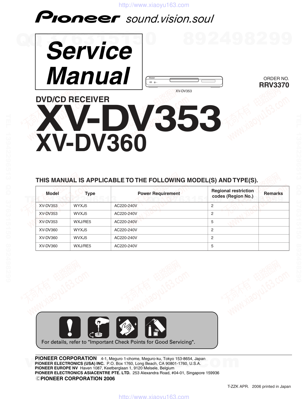
ORDER NO.
PIONEER CORPORATION 4-1, Meguro 1-chome, Meguro-ku, Tokyo 153-8654, Japan
PIONEER ELECTRONICS (USA) INC. P.O. Box 1760, Long Beach, CA 90801-1760, U.S.A.
PIONEER EUROPE NV Haven 1087, Keetberglaan 1, 9120 Melsele, Belgium
PIONEER ELECTRONICS ASIACENTRE PTE. LTD. 253 Alexandra Road, #04-01, Singapore 159936
PIONEER CORPORATION 2006
XV-DV353
RRV3370
DVD/CD RECEIVER
XV-DV353
XV-DV360
THIS MANUAL IS APPLICABLE TO THE FOLLOWING MODEL(S) AND TYPE(S).
Model
Type
Power Requirement
Regional restriction
codes (Region No.)
Remarks
XV-DV353
WYXJ5
AC220-240V
2
XV-DV353
WVXJ5
AC220-240V
2
XV-DV353
WXJ/RE5
AC220-240V
5
XV-DV360
WYXJ5
AC220-240V
2
XV-DV360
WVXJ5
AC220-240V
2
XV-DV360
WXJ/RE5
AC220-240V
5
For details, refer to "Important Check Points for Good Servicing".
T-ZZK APR. 2006 printed in Japan
www. xiaoyu163. com
QQ 376315150
9
9
2
8
9
4
2
9
8
TEL 13942296513
9
9
2
8
9
4
2
9
8
0
5
1
5
1
3
6
7
3
Q
Q
TEL 13942296513 QQ 376315150 892498299
TEL 13942296513 QQ 376315150 892498299
http://www.xiaoyu163.com
XV-DV353
2
1
2
3
4
1
2
3
4
C
D
F
A
B
E
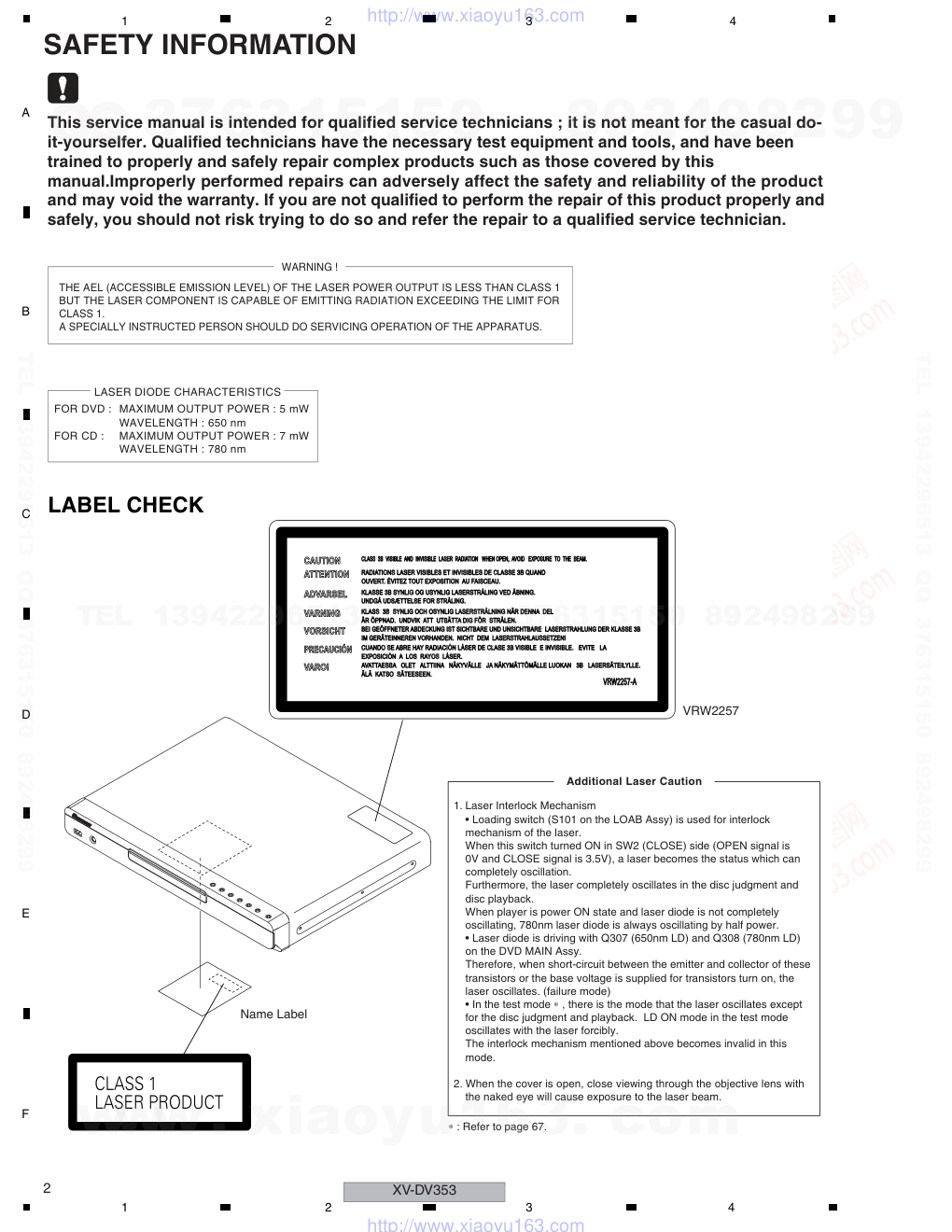
SAFETY INFORMATION
This service manual is intended for qualified service technicians ; it is not meant for the casual do-
it-yourselfer. Qualified technicians have the necessary test equipment and tools, and have been
trained to properly and safely repair complex products such as those covered by this
manual.Improperly performed repairs can adversely affect the safety and reliability of the product
and may void the warranty. If you are not qualified to perform the repair of this product properly and
safely, you should not risk trying to do so and refer the repair to a qualified service technician.
WARNING !
THE AEL (ACCESSIBLE EMISSION LEVEL) OF THE LASER POWER OUTPUT IS LESS THAN CLASS 1
BUT THE LASER COMPONENT IS CAPABLE OF EMITTING RADIATION EXCEEDING THE LIMIT FOR
CLASS 1.
A SPECIALLY INSTRUCTED PERSON SHOULD DO SERVICING OPERATION OF THE APPARATUS.
LASER DIODE CHARACTERISTICS
FOR DVD : MAXIMUM OUTPUT POWER : 5 mW
WAVELENGTH : 650 nm
FOR CD :
MAXIMUM OUTPUT POWER : 7 mW
WAVELENGTH : 780 nm
Additional Laser Caution
1. Laser Interlock Mechanism
• Loading switch (S101 on the LOAB Assy) is used for interlock
mechanism of the laser.
When this switch turned ON in SW2 (CLOSE) side (OPEN signal is
0V and CLOSE signal is 3.5V), a laser becomes the status which can
completely oscillation.
Furthermore, the laser completely oscillates in the disc judgment and
disc playback.
When player is power ON state and laser diode is not completely
oscillating, 780nm laser diode is always oscillating by half power.
• Laser diode is driving with Q307 (650nm LD) and Q308 (780nm LD)
on the DVD MAIN Assy.
Therefore, when short-circuit between the emitter and collector of these
transistors or the base voltage is supplied for transistors turn on, the
laser oscillates. (failure mode)
• In the test mode ∗ , there is the mode that the laser oscillates except
for the disc judgment and playback. LD ON mode in the test mode
oscillates with the laser forcibly.
The interlock mechanism mentioned above becomes invalid in this
mode.
2. When the cover is open, close viewing through the objective lens with
the naked eye will cause exposure to the laser beam.
LABEL CHECK
VRW2257
Name Label
∗ : Refer to page 67.
www. xiaoyu163. com
QQ 376315150
9
9
2
8
9
4
2
9
8
TEL 13942296513
9
9
2
8
9
4
2
9
8
0
5
1
5
1
3
6
7
3
Q
Q
TEL 13942296513 QQ 376315150 892498299
TEL 13942296513 QQ 376315150 892498299
http://www.xiaoyu163.com
XV-DV353
3
5
6
7
8
5
6
7
8
C
D
F
A
B
E
[Important Check Points for Good Servicing]
In this manual, procedures that must be performed during repairs are marked with the below symbol.
Please be sure to confirm and follow these procedures.
1. Product safety
Please conform to product regulations (such as safety and radiation regulations), and maintain a safe servicing environment by
following the safety instructions described in this manual.
1 Use specified parts for repair.
Use genuine parts. Be sure to use important parts for safety.
2 Do not perform modifications without proper instructions.
Please follow the specified safety methods when modification(addition/change of parts) is required due to interferences such as
radio/TV interference and foreign noise.
3 Make sure the soldering of repaired locations is properly performed.
When you solder while repairing, please be sure that there are no cold solder and other debris.
Soldering should be finished with the proper quantity. (Refer to the example)
4 Make sure the screws are tightly fastened.
Please be sure that all screws are fastened, and that there are no loose screws.
5 Make sure each connectors are correctly inserted.
Please be sure that all connectors are inserted, and that there are no imperfect insertion.
6 Make sure the wiring cables are set to their original state.
Please replace the wiring and cables to the original state after repairs.
In addition, be sure that there are no pinched wires, etc.
7 Make sure screws and soldering scraps do not remain inside the product.
Please check that neither solder debris nor screws remain inside the product.
8 There should be no semi-broken wires, scratches, melting, etc. on the coating of the power cord.
Damaged power cords may lead to fire accidents, so please be sure that there are no damages.
If you find a damaged power cord, please exchange it with a suitable one.
9 There should be no spark traces or similar marks on the power plug.
When spark traces or similar marks are found on the power supply plug, please check the connection and advise on secure
connections and suitable usage. Please exchange the power cord if necessary.
0 Safe environment should be secured during servicing.
When you perform repairs, please pay attention to static electricity, furniture, household articles, etc. in order to prevent injuries.
Please pay attention to your surroundings and repair safely.
2. Adjustments
To keep the original performance of the products, optimum adjustments and confirmation of characteristics within specification.
Adjustments should be performed in accordance with the procedures/instructions described in this manual.
4. Cleaning
For parts that require cleaning, such as optical pickups, tape deck heads, lenses and mirrors used in projection monitors, proper
cleaning should be performed to restore their performances.
3. Lubricants, Glues, and Replacement parts
Use grease and adhesives that are equal to the specified substance.
Make sure the proper amount is applied.
5. Shipping mode and Shipping screws
To protect products from damages or failures during transit, the shipping mode should be set or the shipping screws should be
installed before shipment. Please be sure to follow this method especially if it is specified in this manual.
www. xiaoyu163. com
QQ 376315150
9
9
2
8
9
4
2
9
8
TEL 13942296513
9
9
2
8
9
4
2
9
8
0
5
1
5
1
3
6
7
3
Q
Q
TEL 13942296513 QQ 376315150 892498299
TEL 13942296513 QQ 376315150 892498299
http://www.xiaoyu163.com
XV-DV353
4
1
2
3
4
1
2
3
4
C
D
F
A
B
E
CONTENTS
SAFETY INFORMATION..................................................................................................................................... 2
1. SPECIFICATIONS ............................................................................................................................................ 5
2. EXPLODED VIEWS AND PARTS LIST ............................................................................................................ 6
2.1 PACKING ................................................................................................................................................... 6
2.2 EXTERIOR SECTION................................................................................................................................ 8
2.3 06 LOADER ASSY................................................................................................................................... 10
2.4 TRAVERSE MECHANISM ASSY-S ......................................................................................................... 12
3. BLOCK DIAGRAM AND SCHEMATIC DIAGRAM.......................................................................................... 14
3.1 BLOCK DIAGRAM ................................................................................................................................... 14
3.2 LOAB ASSY and OVERALL WIRING CONNECTION DIAGRAM ........................................................... 16
3.3 DVD MAIN ASSY (1/5)............................................................................................................................. 18
3.4 DVD MAIN ASSY (2/5)............................................................................................................................. 20
3.5 DVD MAIN ASSY (3/5)............................................................................................................................. 22
3.6 DVD MAIN ASSY (4/5)............................................................................................................................. 24
3.7 DVD MAIN ASSY (5/5)............................................................................................................................. 26
3.8 DAMP ASSY (1/2).................................................................................................................................... 28
3.9 DAMP ASSY (2/2).................................................................................................................................... 30
3.10 DISPLAY and USB ASSYS.................................................................................................................... 32
3.11 EURO SCART ASSY ............................................................................................................................. 34
3.12 POWER SUPPLY UNIT.......................................................................................................................... 36
3.13 WAVEFORMS ........................................................................................................................................ 38
4. PCB CONNECTION DIAGRAM ..................................................................................................................... 40
4.1 LOAB ASSY............................................................................................................................................. 40
4.2 EURO SCART ASSY ............................................................................................................................... 41
4.3 DVD MAIN ASSY ..................................................................................................................................... 42
4.4 DAMP ASSY ............................................................................................................................................ 46
4.5 DISPLAY and USB ASSYS...................................................................................................................... 48
4.6 POWER SUPPLY UNIT............................................................................................................................ 50
5. PCB PARTS LIST ........................................................................................................................................... 52
6. ADJUSTMENT ............................................................................................................................................... 62
6.1 ADJUSTMENT ITEMS AND LOCATION ................................................................................................. 62
6.2 JIGS AND MEASURING INSTRUMENTS............................................................................................... 62
6.3 NECESSARY ADJUSTMENT POINTS ................................................................................................... 63
6.4 TEST MODE ............................................................................................................................................ 64
6.5 MECHANISM ADJUSTMENT.................................................................................................................. 65
7. GENERAL INFORMATION............................................................................................................................. 67
7.1 DIAGNOSIS ............................................................................................................................................. 67
7.1.1 TEST MODE...................................................................................................................................... 67
7.1.2 DISPLAY SPECIFICATION OF THE TEST MODE............................................................................ 68
7.1.3 FUNCTIONAL SPECIFICATION OF THE SHORTCUT KEY ............................................................ 69
7.1.4 SPECIFICATION OF MODEL INFORMATION DISPLAY .................................................................. 70
7.1.5 FUNCTIONAL SPECIFICATION OF THE SERVICE MODE ............................................................. 71
7.1.6 SERVICE TEST MODE ..................................................................................................................... 72
7.1.7 METHOD FOR DIAGNOSING DEGRADATION OF THE LDS ON THE PICKUP ASSY .................. 75
7.1.8 DVD TROUBLE SHOOTING.............................................................................................................. 76
7.1.9 ID NUMBER AND ID DATA SETTING ............................................................................................... 79
7.1.10 CIRCUIT DESCRIPTION OF DIGITAL AMP. SECTION.................................................................. 82
7.1.11 SPECIFICATIONS FOR THE PROTECTION CIRCUITS FOR THE DIGITAL AMPLIFIER............. 83
7.1.12 PASS/FAIL TEST PROCEDURE OF HDMI TRANSMITTER IC ...................................................... 84
7.1.13 DISASSEMBLY................................................................................................................................ 85
7.2 PARTS...................................................................................................................................................... 92
7.2.1 IC ....................................................................................................................................................... 92
8. PANEL FACILITIES ...................................................................................................................................... 107
www. xiaoyu163. com
QQ 376315150
9
9
2
8
9
4
2
9
8
TEL 13942296513
9
9
2
8
9
4
2
9
8
0
5
1
5
1
3
6
7
3
Q
Q
TEL 13942296513 QQ 376315150 892498299
TEL 13942296513 QQ 376315150 892498299
http://www.xiaoyu163.com
XV-DV353
5
5
6
7
8
5
6
7
8
C
D
F
A
B
E
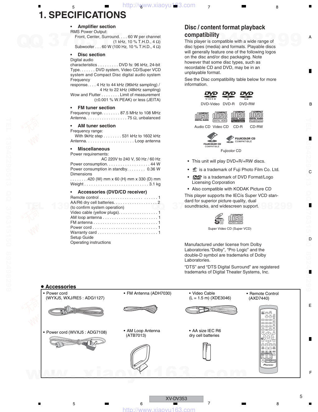
1. SPECIFICATIONS
Accessories
• FM Antenna (ADH7030)
• AM Loop Antenna
(ATB7013)
• Video Cable
(L = 1.5 m) (XDE3046)
• Remote Control
(AXD7440)
• AA size IEC R6
dry cell batteries
Super Video CD (Super VCD)
Disc / content format playback
compatibility
This player is compatible with a wide range of
disc types (media) and formats. Playable discs
will generally feature one of the following logos
on the disc and/or disc packaging. Note
however that some disc types, such as
recordable CD and DVD, may be in an
unplayable format.
See the Disc compatibility table below for more
information.
•
is a trademark of Fuji Photo Film Co. Ltd.
•
is a trademark of DVD Format/Logo
Licensing Corporation
• Also compatible with KODAK Picture CD
This player supports the IECís Super VCD stan-
dard for superior picture quality, dual
soundtracks, and widescreen support.
DVD-Video
DVD-R
DVD-RW
Video CD
Fujicolor CD
Audio CD
CD-R
CD-RW
VIDEO
CD
• This unit will play DVD+R/+RW discs.
Manufactured under license from Dolby
Laboratories.“Dolby”, “Pro Logic” and the
double-D symbol are trademarks of Dolby
Laboratories.
“DTS” and “DTS Digital Surround” are registered
trademarks of Digital Theater Systems, Inc.
TV CONTROL
VOLUME
HOME
MENU
AUDIO
SUBTITLE
ANGLE
ZOOM
STANDBY
/ON
MUTE
LINE
TOP MENU
RETURN
TEST TONE
SOUND
CLEAR
SLEEP
DISPLAY
1
2
3
4
5
6
7
8
9
0
SURROUND
TUNE
TUNE
ST
ST
ENTER
USB
SETUP
MENU
OPEN/
CLOSE
INPUT CHANNEL VOLUME
DVD/CD
TUNER
(FM/AM)
. . . . . . . .420 (W) mm x 60 (H) mm x 330 (D) mm
•
Amplifier section
RMS Power Output:
Front, Center, Surround. . . . 60 W per channel
(1 kHz, 10 % T.H.D., 4 Ω)
Subwoofer . . . 60 W (100 Hz, 10 % T.H.D., 4 Ω)
•
Disc section
Digital audio
characteristics . . . . . . . . . DVD fs: 96 kHz, 24-bit
Type. . . . . . . DVD system, Video CD/Super VCD
system and Compact Disc digital audio system
Frequency
response. . . . 4 Hz to 44 kHz (96kHz sampling) /
4 Hz to 22 kHz (48kHz sampling)
Wow and Flutter . . . . . . . . Limit of measurement
(±0.001 % W.PEAK) or less (JEITA)
•
FM tuner section
Frequency range. . . . . . . . 87.5 MHz to 108 MHz
Antenna. . . . . . . . . . . . . . . . . . 75 Ω, unbalanced
•
AM tuner section
Frequency range:
With 9kHz step . . . . . . . . 531 kHz to 1602 kHz
Antenna. . . . . . . . . . . . . . . . . . . . . Loop antenna
•
Miscellaneous
Power requirements:
AC 220V to 240 V, 50 Hz / 60 Hz
Power consumption. . . . . . . . . . . . . . . . . . . 44 W
Power consumption in standby. . . . . . . . 0.36 W
Dimensions
Weight . . . . . . . . . . . . . . . . . . . . . . . . . . . . 3.1 kg
•
Accessories (DVD/CD receiver)
Remote control . . . . . . . . . . . . . . . . . . . . . . . . . 1
AA/R6 dry cell batteries. . . . . . . . . . . . . . . . . . . 2
(to confirm system operation)
Video cable (yellow plugs). . . . . . . . . . . . . . . . . 1
AM loop antenna . . . . . . . . . . . . . . . . . . . . . . . . 1
FM antenna . . . . . . . . . . . . . . . . . . . . . . . . . . . . 1
Power cord . . . . . . . . . . . . . . . . . . . . . . . . . . . . 1
Warranty card . . . . . . . . . . . . . . . . . . . . . . . . . . 1
Setup Guide
Operating instructions
• Power cord
(WYXJ5, WXJ/RE5 : ADG1127)
• Power cord (WVXJ5 : ADG7108)
www. xiaoyu163. com
QQ 376315150
9
9
2
8
9
4
2
9
8
TEL 13942296513
9
9
2
8
9
4
2
9
8
0
5
1
5
1
3
6
7
3
Q
Q
TEL 13942296513 QQ 376315150 892498299
TEL 13942296513 QQ 376315150 892498299
http://www.xiaoyu163.com
XV-DV353
6
1
2
3
4
1
2
3
4
C
D
F
A
B
E
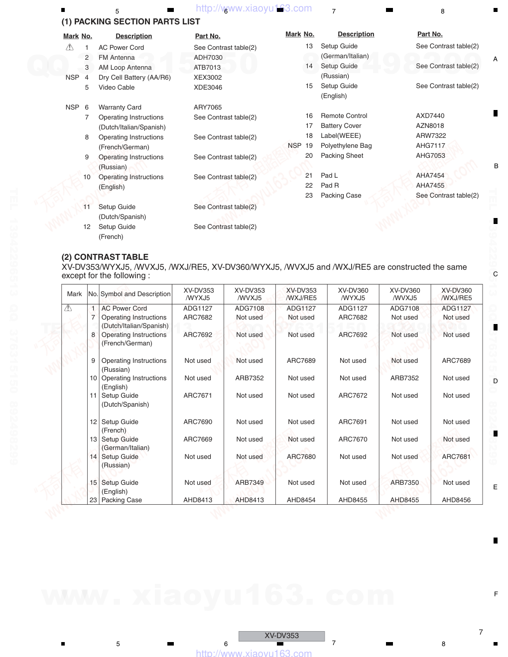
2. EXPLODED VIEWS AND PARTS LIST
2.1 PACKING
Parts marked by "NSP" are generally unavailable because they are not in our Master Spare Parts List.
The mark found on some component parts indicates the importance of the safety factor of the part.
Therefore, when replacing, be sure to use parts of identical designation.
Screws adjacent to mark on product are used for disassembly.
For the applying amount of lubricants or glue, follow the instructions in this manual.
(In the case of no amount instructions, apply as you think it appropriate.)
NOTES:
Front side
Joint of Packing
For WYXJ5 and WXJ/RE5 types
For WVXJ5 type
16
22
20
21
17
18
19
19
3
4
6
7 to 15
1
1
5
2
23
www. xiaoyu163. com
QQ 376315150
9
9
2
8
9
4
2
9
8
TEL 13942296513
9
9
2
8
9
4
2
9
8
0
5
1
5
1
3
6
7
3
Q
Q
TEL 13942296513 QQ 376315150 892498299
TEL 13942296513 QQ 376315150 892498299
http://www.xiaoyu163.com
XV-DV353
7
5
6
7
8
5
6
7
8
C
D
F
A
B
E
(1) PACKING SECTION PARTS LIST
(2) CONTRAST TABLE
XV-DV353/WYXJ5, /WVXJ5, /WXJ/RE5, XV-DV360/WYXJ5, /WVXJ5 and /WXJ/RE5 are constructed the same
except for the following :
Mark No.
Description
Part No.
>
1
AC Power Cord
See Contrast table(2)
2
FM Antenna
ADH7030
3
AM Loop Antenna
ATB7013
NSP
4
Dry Cell Battery (AA/R6)
XEX3002
5
Video Cable
XDE3046
NSP
6
Warranty Card
ARY7065
7
Operating Instructions
See Contrast table(2)
(Dutch/Italian/Spanish)
8
Operating Instructions
See Contrast table(2)
(French/German)
9
Operating Instructions
See Contrast table(2)
(Russian)
10
Operating Instructions
See Contrast table(2)
(English)
11
Setup Guide
See Contrast table(2)
(Dutch/Spanish)
12
Setup Guide
See Contrast table(2)
(French)
13
Setup Guide
See Contrast table(2)
(German/Italian)
14
Setup Guide
See Contrast table(2)
(Russian)
15
Setup Guide
See Contrast table(2)
(English)
16
Remote Control
AXD7440
17
Battery Cover
AZN8018
18
Label(WEEE)
ARW7322
NSP 19
Polyethylene Bag
AHG7117
20
Packing Sheet
AHG7053
21
Pad L
AHA7454
22
Pad R
AHA7455
23
Packing Case
See Contrast table(2)
Mark No.
Description
Part No.
Mark
No. Symbol and Description
XV-DV353
/WYXJ5
XV-DV353
/WVXJ5
XV-DV353
/WXJ/RE5
XV-DV360
/WYXJ5
XV-DV360
/WVXJ5
XV-DV360
/WXJ/RE5
>
1
AC Power Cord
ADG1127
ADG7108
ADG1127
ADG1127
ADG7108
ADG1127
7
Operating Instructions
ARC7682
Not used
Not used
ARC7682
Not used
Not used
(Dutch/Italian/Spanish)
8
Operating Instructions
ARC7692
Not used
Not used
ARC7692
Not used
Not used
(French/German)
9
Operating Instructions
Not used
Not used
ARC7689
Not used
Not used
ARC7689
(Russian)
10 Operating Instructions
Not used
ARB7352
Not used
Not used
ARB7352
Not used
(English)
11 Setup Guide
ARC7671
Not used
Not used
ARC7672
Not used
Not used
(Dutch/Spanish)
12 Setup Guide
ARC7690
Not used
Not used
ARC7691
Not used
Not used
(French)
13 Setup Guide
ARC7669
Not used
Not used
ARC7670
Not used
Not used
(German/Italian)
14 Setup Guide
Not used
Not used
ARC7680
Not used
Not used
ARC7681
(Russian)
15 Setup Guide
Not used
ARB7349
Not used
Not used
ARB7350
Not used
(English)
23 Packing Case
AHD8413
AHD8413
AHD8454
AHD8455
AHD8455
AHD8456
www. xiaoyu163. com
QQ 376315150
9
9
2
8
9
4
2
9
8
TEL 13942296513
9
9
2
8
9
4
2
9
8
0
5
1
5
1
3
6
7
3
Q
Q
TEL 13942296513 QQ 376315150 892498299
TEL 13942296513 QQ 376315150 892498299
http://www.xiaoyu163.com
XV-DV353
8
1
2
3
4
1
2
3
4
C
D
F
A
B
E
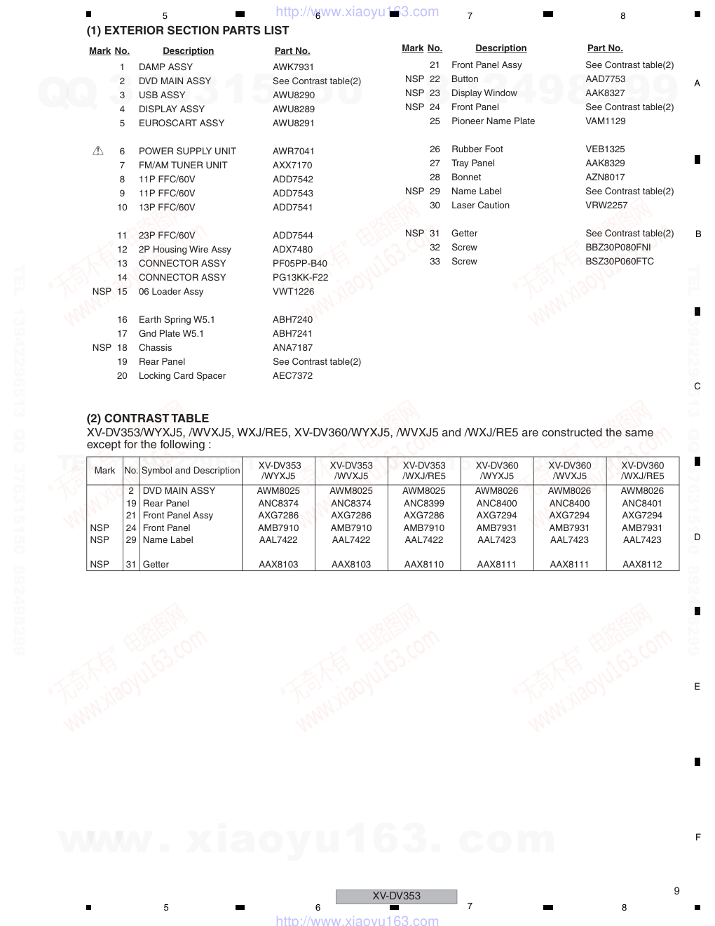
2.2 EXTERIOR SECTION
E
B C
A
32
32
31
16
3
32
17
32
32
32
B C
A
F
F
12
D
30
32
32
10
D
G
G
32
13
E
28
19
32
32
32
32
33
32
32
7
9
8
11
2
5
1
6
14
15
Refer to
"2.3 06 LOADER ASSY".
18
29
32
4
20
22
26
23
27
25
24
21
CONTACT SIDE
NON-CONTACT
SIDE
32
D
E
G
C
F
H
B
www. xiaoyu163. com
QQ 376315150
9
9
2
8
9
4
2
9
8
TEL 13942296513
9
9
2
8
9
4
2
9
8
0
5
1
5
1
3
6
7
3
Q
Q
TEL 13942296513 QQ 376315150 892498299
TEL 13942296513 QQ 376315150 892498299
http://www.xiaoyu163.com
XV-DV353
9
5
6
7
8
5
6
7
8
C
D
F
A
B
E
(1) EXTERIOR SECTION PARTS LIST
(2) CONTRAST TABLE
XV-DV353/WYXJ5, /WVXJ5, WXJ/RE5, XV-DV360/WYXJ5, /WVXJ5 and /WXJ/RE5 are constructed the same
except for the following :
Mark No.
Description
Part No.
1
DAMP ASSY
AWK7931
2
DVD MAIN ASSY
See Contrast table(2)
3
USB ASSY
AWU8290
4
DISPLAY ASSY
AWU8289
5
EUROSCART ASSY
AWU8291
>
6
POWER SUPPLY UNIT
AWR7041
7
FM/AM TUNER UNIT
AXX7170
8
11P FFC/60V
ADD7542
9
11P FFC/60V
ADD7543
10
13P FFC/60V
ADD7541
11
23P FFC/60V
ADD7544
12
2P Housing Wire Assy
ADX7480
13
CONNECTOR ASSY
PF05PP-B40
14
CONNECTOR ASSY
PG13KK-F22
NSP 15
06 Loader Assy
VWT1226
16
Earth Spring W5.1
ABH7240
17
Gnd Plate W5.1
ABH7241
NSP 18
Chassis
ANA7187
19
Rear Panel
See Contrast table(2)
20
Locking Card Spacer
AEC7372
21
Front Panel Assy
See Contrast table(2)
NSP 22
Button
AAD7753
NSP 23
Display Window
AAK8327
NSP 24
Front Panel
See Contrast table(2)
25
Pioneer Name Plate
VAM1129
26
Rubber Foot
VEB1325
27
Tray Panel
AAK8329
28
Bonnet
AZN8017
NSP 29
Name Label
See Contrast table(2)
30
Laser Caution
VRW2257
NSP 31
Getter
See Contrast table(2)
32
Screw
BBZ30P080FNI
33
Screw
BSZ30P060FTC
Mark No.
Description
Part No.
Mark
No. Symbol and Description
XV-DV353
/WYXJ5
XV-DV353
/WVXJ5
XV-DV353
/WXJ/RE5
XV-DV360
/WYXJ5
XV-DV360
/WVXJ5
XV-DV360
/WXJ/RE5
2
DVD MAIN ASSY
AWM8025
AWM8025
AWM8025
AWM8026
AWM8026
AWM8026
19 Rear Panel
ANC8374
ANC8374
ANC8399
ANC8400
ANC8400
ANC8401
21 Front Panel Assy
AXG7286
AXG7286
AXG7286
AXG7294
AXG7294
AXG7294
NSP
24 Front Panel
AMB7910
AMB7910
AMB7910
AMB7931
AMB7931
AMB7931
NSP
29 Name Label
AAL7422
AAL7422
AAL7422
AAL7423
AAL7423
AAL7423
NSP
31 Getter
AAX8103
AAX8103
AAX8110
AAX8111
AAX8111
AAX8112
www. xiaoyu163. com
QQ 376315150
9
9
2
8
9
4
2
9
8
TEL 13942296513
9
9
2
8
9
4
2
9
8
0
5
1
5
1
3
6
7
3
Q
Q
TEL 13942296513 QQ 376315150 892498299
TEL 13942296513 QQ 376315150 892498299
http://www.xiaoyu163.com
XV-DV353
10
1
2
3
4
1
2
3
4
C
D
F
A
B
E
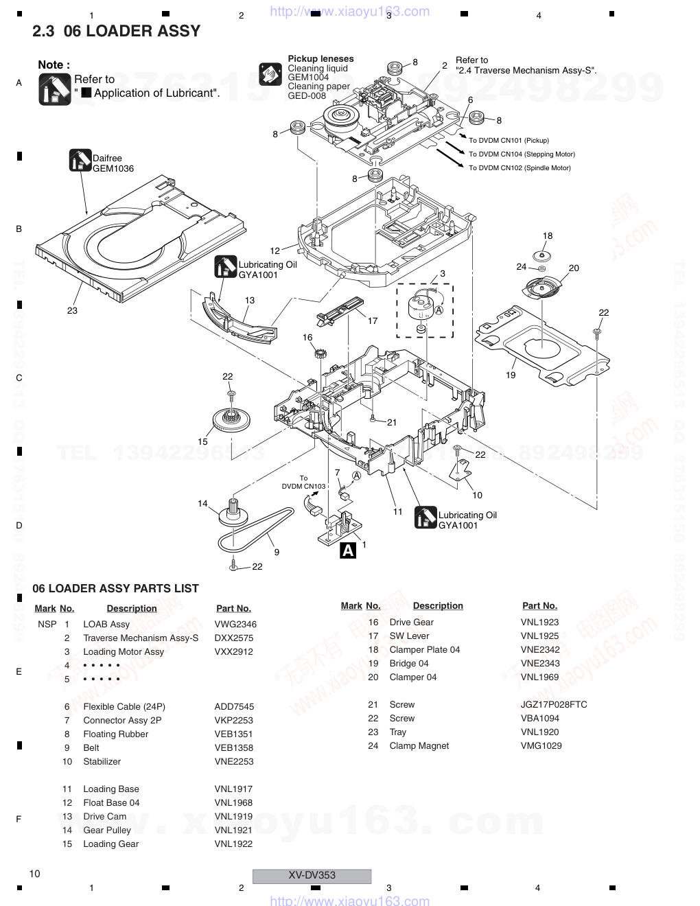
2.3 06 LOADER ASSY
06 LOADER ASSY PARTS LIST
A
A
To DVDM CN101 (Pickup)
To DVDM CN104 (Stepping Motor)
To DVDM CN102 (Spindle Motor)
To
DVDM CN103
2
Refer to
"2.4 Traverse Mechanism Assy-S".
3
12
23
13
17
21
16
22
15
14
22
22
22
20
19
9
1
7
10
11
6
8
8
8
8
18
24
A
Lubricating Oil
GYA1001
Daifree
GEM1036
Refer to
" Application of Lubricant".
Note :
Lubricating Oil
GYA1001
Pickup leneses
Cleaning liquid
GEM1004
Cleaning paper
GED-008
Mark No.
Description
Part No.
NSP
1
LOAB Assy
VWG2346
2
Traverse Mechanism Assy-S
DXX2575
3
Loading Motor Assy
VXX2912
4
• • • • •
5
• • • • •
6
Flexible Cable (24P)
ADD7545
7
Connector Assy 2P
VKP2253
8
Floating Rubber
VEB1351
9
Belt
VEB1358
10
Stabilizer
VNE2253
11
Loading Base
VNL1917
12
Float Base 04
VNL1968
13
Drive Cam
VNL1919
14
Gear Pulley
VNL1921
15
Loading Gear
VNL1922
16
Drive Gear
VNL1923
17
SW Lever
VNL1925
18
Clamper Plate 04
VNE2342
19
Bridge 04
VNE2343
20
Clamper 04
VNL1969
21
Screw
JGZ17P028FTC
22
Screw
VBA1094
23
Tray
VNL1920
24
Clamp Magnet
VMG1029
Mark No.
Description
Part No.
www. xiaoyu163. com
QQ 376315150
9
9
2
8
9
4
2
9
8
TEL 13942296513
9
9
2
8
9
4
2
9
8
0
5
1
5
1
3
6
7
3
Q
Q
TEL 13942296513 QQ 376315150 892498299
TEL 13942296513 QQ 376315150 892498299
http://www.xiaoyu163.com
XV-DV353
11
5
6
7
8
5
6
7
8
C
D
F
A
B
E
Application of Lubricant
Lubricating Oil
GYA1001
Around the shaft
No. 11
Loading Base
No. 13
Drive Cam
No. 13
Drive Cam
No. 23
Tray
No. 23
Tray
Front View
Rear View
Daifree
GEM1036
Inner side of a ditch
Concave of unevenness
Top View
Bottom View
Daifree
GEM1036
Daifree
GEM1036
Side of the rib
Concave of unevenness
Daifree
GEM1036
Concave of unevenness
Daifree
GEM1036
Inner side of a ditch
Lubricating Oil
GYA1001
Inner side of a ditch
Lubricating Oil
GYA1001
Lubricating Oil
GYA1001
Lubricating Oil
GYA1001
Lubricating Oil
GYA1001
Lubricating Oil
GYA1001
www. xiaoyu163. com
QQ 376315150
9
9
2
8
9
4
2
9
8
TEL 13942296513
9
9
2
8
9
4
2
9
8
0
5
1
5
1
3
6
7
3
Q
Q
TEL 13942296513 QQ 376315150 892498299
TEL 13942296513 QQ 376315150 892498299
http://www.xiaoyu163.com
XV-DV353
12
1
2
3
4
1
2
3
4
C
D
F
A
B
E
2.4 TRAVERSE MECHANISM ASSY-S
To
DVDM CN101
(Pickup Assy)
To
DVDM CN104
(Stepping Motor)
To DVDM CN102
(Spindle Motor)
CONTACT SIDE
NON-CONTACT
SIDE
13
8
10
10
11
11
12
2
4
1
3
6
9
5
14
7
Silicone Adhesive
GEM1037
Note : When part #2 replaced,
part #13 also need to be
replaced at the same time.
Note : Spindle screw (DBA1252) of No.13 is the screw which applied special bond.
Therefore the adhesion becomes inteffective when takes it off once. Spindle screw is the part which cannot recycle.
When part #2 is replaced, part #13 also need to be replaced at the same time.
Refer to
" Application of Lubricant".
Note :
www. xiaoyu163. com
QQ 376315150
9
9
2
8
9
4
2
9
8
TEL 13942296513
9
9
2
8
9
4
2
9
8
0
5
1
5
1
3
6
7
3
Q
Q
TEL 13942296513 QQ 376315150 892498299
TEL 13942296513 QQ 376315150 892498299
http://www.xiaoyu163.com
XV-DV353
13
5
6
7
8
5
6
7
8
C
D
F
A
B
E
TRAVERSE MECHANISM ASSY-S PARTS LIST
Mark No.
Description
Part No.
>
1
06SD Pickup Assy
OXX8020
2
Spindle Motor N200
DXM1197
3
Guide Shaft VK1
DLA1940
4
Sub Guide Shaft VK1
DLA1941
NSP
5
Joint VK1B
DNK4272
6
Joint Spring VK1
DBK1235
7
Stepping Motor VK1
DXM1201
NSP
8
Mechanism Frame VK1
DNK4160
9
Precision Screw VK1
DBA1209
10
Skew Screw VK1
DBA1211
11
Skew Spring VK1
DBH1516
NSP 12
Stepping Screw
DBA1205
13
Spindle Screw VK1(for Service) DBA1252
NSP 14
Hold Spring
DBK1297
www. xiaoyu163. com
QQ 376315150
9
9
2
8
9
4
2
9
8
TEL 13942296513
9
9
2
8
9
4
2
9
8
0
5
1
5
1
3
6
7
3
Q
Q
TEL 13942296513 QQ 376315150 892498299
TEL 13942296513 QQ 376315150 892498299
http://www.xiaoyu163.com
XV-DV353
14
1
2
3
4
1
2
3
4
C
D
F
A
B
E
3. BLOCK DIAGRAM AND SCHEMATIC DIAGRAM
3.1 BLOCK DIAGRAM
RESET
SCL
SDA
MUTE
PDN
SD
OTW
BE
MT1389
64M
SDRAM
8M
FLASH
16k
EEPROM
MOTOR
DRIVER
LOADER
MECHA
A/D
AK5358VT
FL
Display
Driver
KEY
LINE/TV
SCART
TUNER
• AUDIO PROCESSING
-Audio Decode
-Bass Management
-Virtual Surround
-Preset EQ
etc.
ALRCK
ACLK
ASDAT1
ASDAT0
ASDAT2
ADLRCK
ADMCK1
ADBCK
ADDATA
12.288M
74HCU04
G,B,R
Y,C
V
+9V
EV5V
LRCKO
MCLK
USB POWER
USB DP
USB DM
BCKO
DATAO
MCKO
FL DC+/-
-25.5V
PCON(fromSMPSorD-AMP)
DC DET
1.8V
SW
9V
5V
27M
6.8V
5V
LINE
SCART
SW+10.5V
DVD POWER
+9V
ADMCK0
PWRCONT
SW3.3V(A)
V+3
EV+5V
V+5
V+1R8
SW5.0V
V+5V
SW
SW
SYSTEM
µ-com
DVD MAIN ASSY
B
DISPLAY ASSY
D
USB
ASSY
E
LOAB ASSY
A
FM/AM
TUNER
UNIT
H
www. xiaoyu163. com
QQ 376315150
9
9
2
8
9
4
2
9
8
TEL 13942296513
9
9
2
8
9
4
2
9
8
0
5
1
5
1
3
6
7
3
Q
Q
TEL 13942296513 QQ 376315150 892498299
TEL 13942296513 QQ 376315150 892498299
http://www.xiaoyu163.com
XV-DV353
15
5
6
7
8
5
6
7
8
C
D
F
A
B
E
HP AMP
SCART
Composite
HDMI OUT
FRONT L
FRONT R
CENTER
SUB WOOFER
REAR L
REAR R
LINE
LPF
Video
AMP
G, B, R
G, B, R
Y, C
V
Y, C
V
Scart
Circuit
+B
+3.3V
MODULATER
TAS5508
DRIVER
TAS5122
RESET
PWMA P
PWMB P
SD
PWMA M
PWMB M
ch7 ch8 PWM
HP SEL
HDMI
Transmitter
TX
LINE
SCART
EV5.0V
SW 5.0V
GND +B
SW 3.3V (B)
SW3.3V (A)
SW 6.8V
SW 10.5V
GND
-25.5V
FLDC +-
AC IN
DAMP ASSY
C
POWER SUPPLY UNIT
G
www. xiaoyu163. com
QQ 376315150
9
9
2
8
9
4
2
9
8
TEL 13942296513
9
9
2
8
9
4
2
9
8
0
5
1
5
1
3
6
7
3
Q
Q
TEL 13942296513 QQ 376315150 892498299
TEL 13942296513 QQ 376315150 892498299
http://www.xiaoyu163.com
XV-DV353
16
1
2
3
4
1
2
3
4
C
D
F
A
B
E
3.2 LOAB ASSY and OVERALL WIRING CONNECTION DIAGRAM
ADX7480-
PF05PP-B40
CN1
CN1
B2P-VH
S5B-PH-K-S
B5B-PH-K-S
VKN1235
B13B-PH-K-S
B13B-PH-K-S
VKN2045
OKN8001
VKN1243
CKS3376-
GND
+B
AC POWER CORD
LIVE
NEUTRAL
SW3.3V(A)
Pwr-ctr
GND
FL DC+
-25.5V
FL DC-
OWY8087-
FOCS RTN
TRKG RTN
FOCS DRV
TRKG DRV
FOCS RTN
FOCS DRV
TRKG RTN
PICK UP ASSY
TRKG DRV
VWG2346-
LOAB ASSY
SW3.3V(A)
FL DC-
GNDD
FL DC+
GND
VSHF
GNDD
LD(780)
PD
LD(650)
Pwr-ctr
-25.5V
GNDD
LD(650)
PD
LD(780)
GNDD
VSHF
SW1
SW1
SW2
GNDD
LOAD+
LOAD-
GNDD
LOAD-
LOAD+
SW2
STEPPING MOTOR
4P FFC
ST2+(B)
ST2-(~B~)
ST1-(~A~)
ST1+(A)
ST1+(A)
ST1-(~A~)
ST2-(~B~)
ST2+(B)
SW6.8V
GND
SW3.3V(B)
SW5.0V
SW10.5V
EV5.0V
AC_DET
PG13KK-F22
( )
KU,GA BASE
EU,J,
TXR
GND
RDS
VSM
GND
SW(DVD/CD)
A
VR650
B
RF
SW5.0V
VR780
EV5.0V
VRCOM
SW6.8V
SW3.3V(B)
SW10.5V
SW(DVD/CD)
(ADD7545-)
24P FFC
A
VR650
B
RF
VR780
VRCOM
D
C
AC_DET
EU,J,
( )
KU,GA BASE
F
VCC
E
VS(VREF)
C
D
VS(VREF)
E
VCC
F
GNDD
DVD LOADER
GNDD
VWT1226-
V+5S
U-
V+
U+
U+
U-
V+
V+5S
W-
12P FFC
HB
V
W+
V-
U
SPINDLE MOTOR
W-
U
V-
W+
V
HB
INSIDE
W
W
INSIDE
TXR
VSM
RDS
GND
AM
FM
DO
DI
CE
GND
TXL
CLK
+9V
11P FFC
(ADD7543)
+9V
CLK
CE
DI
DO
TXL
GND
1
2
2
1
9
8
13
11
12
10
12
13
12
12
13
13
10
11
11
10
11
10
8
9
9
8
9
8
24
21
22
23
20
18
19
15
14
16
17
5
5
3
4
1
2
2
3
4
1
1
3
2
4
3
2
4
5
6
7
6
7
6
7
6
7
5
4
4
5
4
5
2
3
2
3
3
2
1
1
1
1
8
11
9
10
13
11
12
10
9
8
2
3
4
5
7
6
1
2
3
4
1
6
5
9
7
10
8
12
11
1
2
3
4
7
5
6
CN2
CN1
CN601
CN104
CN103
CN3
CN1001
CN101
CN102
CN5701
CN602
2
1
LOADING
MOTOR ASSY
: VXX2912
LOAB ASSY
(VWG2346)
A
No schematic Diagram
FM/AM TUNER
UNIT
(AXX7170)
H
B B
B
( 1/5- 4/5)
(AWM8026:XV-DV360)
(AWM8025:XV-DV353)
POWER
SUPPLY UNIT
(AWR7041)
G
DVD MAIN ASSY
www. xiaoyu163. com
QQ 376315150
9
9
2
8
9
4
2
9
8
TEL 13942296513
9
9
2
8
9
4
2
9
8
0
5
1
5
1
3
6
7
3
Q
Q
TEL 13942296513 QQ 376315150 892498299
TEL 13942296513 QQ 376315150 892498299
http://www.xiaoyu163.com
XV-DV353
17
5
6
7
8
5
6
7
8
C
D
F
A
B
E
Vout
GND
Vcc
REMOCON
FLCS
FLCK
FLDATA
VE+5
GNDD
FLDC+
FLDC-
KEY2
KEY1
GNDD
GNDD
VFDP
FLDATA
FLCK
FLCS
VFDP
GNDD
VE+5
GNDD
KEY1
KEY2
FLDC-
FLDC+
GNDD
HEAD PHONE
B2P-VH
AKE7121
AKP7199-
AKM7077-
AKP7199-
AKM7077-
RPM7540-H9
CKS3378-
CKS3376-
CKS3378-
CKS3376-
CKS3388-
XKB3062
AKN7003-
CKS3388-
VKB1122
AKP7210-
XKB3054-
GND
GND
S_TVOUT_L
LIN1_L
GND
GND
GND
S_TVOUT_R
LIN1_R
FANCONT
RECMUTE
FAN CONT/GND *
S_TVOUT_R
RECMUTE
S_TVOUT_L
GND
GND
LIN1_R
LIN1_L
GND
LRCLK
MCLK
GND
SDATA3
SDATA2
GND
SCLK
SDATA1
GND
LRCLK
SCLK
GND
GND
MCLK
GND
SDATA3
SDATA2
SDATA1
GND
+B
*
CN3102 2P
AWK7934
AWK7933
AWK7932
AWK7931
GND
FAN CONT
SW-
SW+
FL-
RL+
C+
C-
RL-
FL+
6ch SP OUT
FR+
RR-
RR+
FR-
SCL
XSD
XOTW
GND
GND
POWER
GND
GND
XSD
POWER
GND
GND
SCL
XOTW
XMUTE
3.3V
SDA
GND
HPR
GND
XPDN
GND
XRST
GND
SDA
XMUTE
3.3V
XRST
XPDN
HPR
GND
GND
XHPSEL
PCON
HPL
PCON
HPL
XHPSEL
AAV7104(AAV7107)
FL
13P FFC(ADD7541)
V5USB
GNDUSB
HP_DET
HP_L
GNDD
HP_R
HPMUTE
(ADD7542)
USB_DM2
USB_DP2
V5USB
11P FFC
V5USB
V5USB
GNDUSB
HP_R
HPMUTE
USB_DM2
HP_L
USB_DP2
HP_DET
GNDD
S_Y
TVIN_R
USB
(RKB1041)
TVIN_L
XKP3086
JA602
HP OUT
GNDUSB
GNDUSB
S_Y
NC
V
GND
COMPOSITE
VIDEO
OUTPUT
GND
S_C
GND
GND
GND
DVDPOWER
CLOCK SHIELD
CLOCK+
DATA0-
DATA0 SHIELD
DATA0+
DATA1-
DATA1 SHIELD
DATA1+
DATA2-
DATA2 SHIELD
DATA2+
+5V
TVOUT_L
SCART_R
HOT PLUG DETECT
SCART_L
DDC/CEC GND
TVMUTE
HDMISCL
V+5
CEC
CLOCK-
VSEL2
HDMISDA
GND
GND
(AKP7211)
HDMI OUTPUT
VSEL1
SQEEZE
NC
V+10
TVOUT_R
V
V
GND
GND
R
23P FFC
R
DVDPOWER
S_C
G
G
GND
GND
R/C
BLANK
GND
GND
GND
GND
V/Y
G
NC
B
(ADD7544)
B
VSEL2
V+5
GND
SCART_L
SCART_R
GND
TVOUT_R
TVOUT_L
TVMUTE
R IN
B
L OUT
GND
GND
L IN
SQUEEZE
NC
GND
VSEL1
V+10
SQEEZE
EURO CONNECTOR
R OUT
1
1
4
3
2
4
3
2
6
7
5
6
7
5
10
9
8
10
9
8
13
11
12
13
11
12
15
16
14
15
16
14
17
19
18
19
17
18
2
1
12
11
5
8
9
6
7
10
2
1
3
4
1
1
4
3
2
4
3
2
6
5
7
6
5
7
10
9
8
10
9
8
13
11
12
11
12
13
15
16
14
15
16
14
17
18
19
18
19
17
3
2
1
4
5
6
9
10
7
8
13
11
12
4
1
2
3
7
8
5
6
9
10
10
13
11
12
3
2
1
4
6
9
7
8
5
8
2
3
4
7
6
11
9
10
5
11
1
23
23
20
21
7
2
1
11
6
5
4
3
10
9
8
15
16
13
14
19
17
18
12
20
21
22
20
21
22
19
17
18
19
17
18
14
15
16
14
15
16
17
18
15
16
13
14
12
11
19
13
12
11
13
12
11
10
9
8
10
9
8
7
6
5
7
6
5
2
8
7
6
5
10
9
4
3
2
3
4
2
3
4
1
1
1
CN3201
CN3211
CN3002 CN3102
CN3001 CN3101
IC5902
CN5901
CN5902
CN5602
CN5601
JA3111
JA5902
CN451
CN461
JA403
CN931
JA451
C C
C
( 1/2- 2/2)DAMP ASSY
(AWK7931)
E
USB ASSY
(AWU8290)
F
EURO SCART
ASSY
(AWU8291)
D
DISPLAY ASSY
(AWU8289)
÷ When ordering service parts, be sure to refer to "EXPLODED VIEWS and PARTS LIST" or
"PCB PARTS LIST".
÷ The > mark found on some component parts indicates the importance of the safety factor
of the part. Therefore, when replacing, be sure to use parts of identical designation.
÷
: The power supply is shown with the marked box.
www. xiaoyu163. com
QQ 376315150
9
9
2
8
9
4
2
9
8
TEL 13942296513
9
9
2
8
9
4
2
9
8
0
5
1
5
1
3
6
7
3
Q
Q
TEL 13942296513 QQ 376315150 892498299
TEL 13942296513 QQ 376315150 892498299
http://www.xiaoyu163.com
XV-DV353
18
1
2
3
4
1
2
3
4
C
D
F
A
B
E
3.3 DVD MAIN ASSY (1/5)
USB POWER CONTROL
A13
A15
A14
A9
A8
A12
A10
A11
~BYTE~
A16
VSS
D6
D7
D15
D14
A19
~WE~
NC
~RESET~
NC
NC
A18
RY/~BY~
A6
A4
A5
A7
A17
A3
A1
A2
AYW7096
D12
D5
D13
D4
VCC
D10
D3
D11
D2
D9
D0
D8
D1
VSS
~OE~
A0
~CE~
SW1
SW2
GNDD
LOAD-
LOAD+
to LOAB ASSY
ST1-(~A~)
ST1+(A)
ST2+(B)
to STEPPING MOTOR
ST2-(~B~)
FCO+
LDOP
LDON
FCO-
AGND
AVM
TKO+
TKO-
SERVO DRIVER
V+5S
U+
U-
V+
V-
VCC
HU+
HU-
HV+
HV-
HB
HW+
HW-
W-
W+
U
HB
W
V
to SPINDLE MOTOR
INSIDE
FOCS RTN
TRKG RTN
FOCS DRV
TRKG DRV
VSHF
GNDD
LD(650)
LD(780)
PD
VR780
GNDD
SDA
SCL
WP
GND
NC
NC
VCC
NC
3.3v
1.8v
IOA19 (PU)
IOA18 (PU)
HIGHA0(PU)
HIGHA6(PU)
HIGHA4(PU)
HIGHA3(PU)
HIGHA5(PU)
HIGHA2(PU)
HIGHA1(PU)
IOA20
IOA7 (PU)
IOA5 (PU)
IOA6 (PU)
IOA4 (PU)
IOA3 (PU)
IOA2 (PU)
TCK/V_ADIN6 (JTAG)
TDO/V_ADIN7 (JTAG)
DVDD18
65:DVDD3
66:IOWR#
67:A16
68:HIGHA7(PU)
TKIN
FCIN
LDIN
DVCC
SLO1P
SLGND
SLVDD
SLO1N
SLIN2
SLIN1
SLRNF2
SLO2N
SLO2P
SLRNF1
U
SPGND1
V
SPVM1
W
SPGND2
SPVM1
SPRNF
CTL1
CTL2
DGND
FG
SPIN
VC
TMS/V_ADIN5 (JTAG)
TDI/V_ADIN4 (JTAG)
FG/V_ADIN8 (PU)
USB_VDD3
USBM
USBP
VPLLVDD3
CAPPAD
USB_VSS
TRO
FOO
VPLLVSS
PWMOUT1/V_ADIN9
TROPENPWM
FMO
OP_INP
OP_INN
DMO
TEO
OP_OUT
TEZISILV
V2REFO
FEO
VREFO
V2O
SGND
RFLV/RFON
CSO/RFOP
(1/2)
(2/2)
6
3
2
4
1
5
(1/2)
6
3
2
4
1
5
SVDD3
LDO1
LDO2
MIDI2
MIDI1
TPI
CDFON
CDFOP
TNI
3.3v
SD
SC
SB
MD
MC
SA
MB
MA
DVDRFIN
RFGC:254
AVDD3:256
OSN:253
IREF:255
DVDC
DVDRFIP
DVDD
AGND
DVDA
DVDB
OSP
RFRPAC
CRTPLP
RFGND
HRFZC
RFRPDC
VR650
VRCOM
A
B
SW
RF
(2SC4081(QR))
C
D
VCC
E
F
VREF
GNDD
to PICK UP
(2/2)
1.8v
3.3v
CTL
XFLAG
PWR#
PCE#
A14
A16
A15
A10
A13
A9
A11
A12
A17
AD7
A0
AD6
PWR#
A20
A19
A5
A18
A8
A7
A6
A3
A2
A4
AD5
AD1
AD3
AD2
AD0
AD4
PRD#
PCE#
A1
A16
A14
A15
PWR#
A10
A13
A11
A12
A9
A20
TROUT
TRIN
LOAD+
LOAD-
LOAD-
LOAD+
F+
F-
T+
T-
ST2+
ST1+
ST1-
ST2-
HV-
HU-
HU+
HV+
HW-
W
U
HW+
V
HU-
HU+
HV-
HW+
HW-
HV+
T+
F+
F-
T-
SDA
SCL
ST1-
ST2+
ST1+
ST2-
TRSO
FOSO
TROPEN
A19
A8
A18
FMSO
PWMOUT1
ENDM
STBY
A4
A5
A3
A2
A6
A7
TROUT
FG
TRIN
FOSO
TRSO
TROPEN
FMSO
PWMOUT1
DMSO
DMSO
STBY
ENDM
FG
W
U
V
MDI1
LDO1
E
LDO2
F
LDO2
B
C
RF
D
A
LDO1
SUBC
SUBD
SUBB
SUBA
MDI1
A
B
IOA
RF
D
C
E
F
IOA
IOA
3
1
2
4
5
1
3
2
1
2
3
8
6
7
4
5
48
47
46
42
43
45
44
41
4
3
2
1
11
10
9
12
15
16
14
13
19
18
17
20
21
23
24
22
38
37
39
40
34
35
36
33
28
31
29
30
32
26
25
27
5
3
4
1
2
4
3
2
1
1
3
2
6
4
7
5
8
1
2
3
4
5
43
44
42
37
38
39
40
41
6
7
8
9
10
11
12
24
22
23
20
21
18
19
16
17
15
14
5
1
2
5
6
7
4
3
2
8
1
63
62
64
65
68
67
66
72
73
70
71
69
75
74
61
59
60
56
57
58
55
53
54
10
11
12
9
14
15
16
13
21
20
17
18
19
22
33
35
34
36
31
30
32
29
26
27
24
25
28
23
50
51
52
48
49
47
45
44
46
41
43
42
40
38
39
37
35
36
33
34
32
31
29
30
28
27
26
24
25
23
21
20
22
17
19
18
15
16
13
14
10
11
12
8
9
7
5
6
4
2
1
3
253
256
254
255
248
252
250
251
249
247
12
13
11
10
9
8
4
3
7
6
4
5
2
3
1
V+5USB
USBN
USBP
XFLAG
USBPOWER
V+6R8
LIMIT
V+5M
V+5S
V+1R8
V+3
C772
C773
C771
IC771
R771
R772
L772
C781
C783
C782
IC781
R285
R284
D781
D782
IC203
C289
L761
C296
R282
KN103
CN104
R131
R134
R135
R133
R132
R136
C153
C152
C151
C103
CN103
C133
C101
IC101
C140
C102
C141
C142
C143
CN102
R318
R219
R218
R208
R151
R153
R154
R152
C104
C121
IC204
C290
R232
C221
C220
R217
R211
R210
C217
C131
C132
R214
C144
C161
C209
C212
C145
C146
C210
C208
C211
R213
R212
R770
R768
C216
R769
C218
R767
C219
R205
R206
R204
R202
R201
C206
C200
C205
C204
C213
C203
C215
R239
R238
Q307
Q307
R322
R325
C309
L308
L309
Q308
C310
C344
C345
C347
C343
C346
C207
C214
C201
C202
C268
C269
R371
R372
R373
R374
Q305
R315
R313
Q304
R314
R375
C371
C373
C372
CN101
C374
R321
R326
C320
R310
Q308
R200
C273
R207
C271
C272
R256
C267
R255
C265
0.1/16
1/16
GNDD
AAT4618IGV-0.5-1-TLB
STBY
100k
ATL7002-A-T
220
10/50
STBY
2.2
NJM2845DL-05
V+5USB
***
10k
GNDD
S29AL016D70TFI010
STBY
STBY
GNDD
V+3D
FLASH
V+6R8
V+3D
1000p
1
***
S-24CS04AFJ
STBY
GNDD
B5B-PH-K-S
0.01
0.01
0.01
YB
YB
YB
GNDM
VKN1235
GNDD
4.7
4.7
4.7
4.7
4.7
4.7
***
1
100/10
BD7995EFS
1
V+5S
1
V+6R8
***
***
***
VKN1243
GNDD
100K
VTH1047
10K
10K
STBY
1
V+3D
V+3
1.8
1.8
1
1
V+5M
EEPROM
0.1
STBY
***
0.1
STBY
0.1
STBY
STBY
1
0.1
***
***
2200p
1000p
V1P4
0.1
100p
2200p
2200p
2200p
V20
V1P4
2200p
10K
10K
33
0.1
15k
33
0.1
5600p
15k
51k
51k
22k
22K
100p
1.5K
47/35
0.1
0.1
0.1
0.1
47/35
47/35
HN1A01F(YGR)
HN1A01F(YGR)
4.7
4.7
47/35
***
***
HN1A01F(YGR)
47/35
GNDD
STBY
0.1
STBY
1
1
1
1
1
STBY
220/6.3
220/6.3
0.033
***
***
***
***
UM5K1N
GNDD
10K
100K
2SC4154(EFG)
10K
***
0.1
STBY
0.1
V+5S
VKN2045-
GNDD
100/6.3
V+5S
V20
4.7
4.7
HN1A01F(YGR)
***
V+3
STBY
STBY
V+1R8
0.1
STBY
0.1
0.1
0.1
15k
1000p
V+3
100K
22p
V1P4
OUT
IN
3-C1
3-C1
3-B4
3-C2
B 1/5
TRAVERSE MECHA ASSY CN1
SPINDLE MOTOR
STEPPING
MOTOR
(RF)
(T)
(T)
(F)
(F)
(S)
(S)
(S)
(S)
LD CURRENT
CONTROL
FTS Driver
FLASH
(T)
(F)
(T)
(F)
(RF)
B 3/5
B 3/5
CN601
A
4
2
1
3
www. xiaoyu163. com
QQ 376315150
9
9
2
8
9
4
2
9
8
TEL 13942296513
9
9
2
8
9
4
2
9
8
0
5
1
5
1
3
6
7
3
Q
Q
TEL 13942296513 QQ 376315150 892498299
TEL 13942296513 QQ 376315150 892498299
http://www.xiaoyu163.com
XV-DV353
19
5
6
7
8
5
6
7
8
C
D
F
A
B
E
XREADY
MDATA
SCLK
ACK
SDATA
DOWNLOAD
XDVDRST
XIOCS
IOA1
XIOCE
AD0
AD1
DVSS
AD2
AD4
AD5
AD3
AD6
DVSS
AD7
ALE
IOA21
3.3v
1.8v
*1
*1
1.8v
3.3v
DVDD18
IOA0
A17
URD#
UWR#
DVDD3
UP1_4 (PU)
UP1_3 (PU)
UP1_2 (PU)
UP3_0 (PU)
UP1_7 (PU)
UP1_5 (PU)
UP1_6 (PU)
ICE (PD)
XPRST
UP3_4 (PU)
UP3_5 (PU)
UP3_1 (PU)
IR
XINT0
IO_19
DQM0
RD6
RD7
RD4
RD5
DVDD3
RD3
RD0
RD1
RD2
RD14
RD13
RD15
RD12
DVDD3
RD8
IO_18
126:RD11
127:RD10
128:RD9
DQM1
XCAS
XRWE
XRAS
BA0
BA1
XRCS
RA10
RA0
RA2
RA1
DVDD18
DVDD3
RA3
DVSS
CKE
RA11
RCLK
RA7
RA4
Y7/IO_16
DVDD3
RA6
RA5
Y6/IO_16
RA9
RA8
C7/IO_7
C6/IO_6
DVDD18
Y5/IO_14
Y4/IO_13
Y3/IO12
YUVCLK/IO_8
Y2/IO11
Y2/IO10
Y1/IO9
ADCVSS
RFVDD3
ADCVDD3
LPFON
PLLVDD3
LPFIP
LPFOP
LPFIN
JITFO
JITFN
IDACEXLP
PLLVSS
RFVDD18
XTALI
XTALO
RFGND18
C5/IO_5
DVDD3
IO_17
C0/IO_0
C2/IO_2
C3/IO_3
C4/IO_4
DVDD18
C1/IO_1
YUV6/R
YUV5/B
VSYNC/V_ADIN1
DACVSSA
YUV4/G
YUV1/Y:191
DACVDDB:190
DVSS
HSYNC/VADIN2
YUV7
DACVDDA
DACVSSC:192
YUV2/C:189
AL/SDATA2
ALF/(CTR)
ALS/SDATA0
AR/SDATA1
ARS/SDATA3
ADACVDD2
ADACVDD1
ARF(SW)
AVCM
APLLCAP
ADACVSS2
ADACVSS1
APLLCSS
SPDIF
MC_DATA
DVDD18
ASDATA4
APLLVDD3
ACLK
ABCK
ALRCK
ASDATA3
SPBCLK
SPDATA
SPLRCK
DVDD3
ASDATA1/GPO_1
ASDATA2/GPO_0
YUV3/CVBS
RCLKB/GPIO_5
RVREF/GPIO_6
ASDATA0/GPO_2
DACVSSB
SPMCLK
GPIO_4
GPIO_3
DACVDDC
VREF
FS
YUV0/CIN
VSS
VSSQ
DQ14
DQ15
VCC
VCCQ
DQ1
DQ0
DQ13
VCCQ
DQ12
VSSQ
DQ11
DQ10
DQ8
VCCQ
DQ9
DQ3
DQ2
VSSQ
VCCQ
DQ4
DQ5
DQ6
DQ7
VSSQ
VSS
NC
UDQM
NC
CLK
CKE
A11
A9
A8
VCC
LDQM
WE
CS
RAS
CAS
BA0
BA1
A10/AP
A6
A7
A5
VSS
A4
A0
A1
A2
VCC
A3
3.3v
1.8v
EU,KUC,GA UPPER
CH:CCSRCH~
OTHERS:CKSRYB~
:1608 Size
: 2125 Size
CKSQ**~
CAPACITOR
:1608 Size
RS1/10S***J
(F):RS1/16S****F
OTHERS:RS1/16S***J
1.8v
*1
*1
*1
3.3v
1.8v
3.3v
RESISTOR
: 2125 Size
Chip Size
to VIDEO PART
(Page 2/2)
to AUDIO PART
(Page 2/2)
78
PRD#
A1
PCE#
AD0
AD2
AD1
AD5
AD6
AD4
AD3
A17
AD7
50
67
51
49
80
A0
SDA
HDMISCL
SCL
HDMISDA
XDVDRST
INT0#
HDMI
TXD
RXD
DQM0
DQ7
DQ4
DQ3
DQ6
DQ5
DQ1
DQ0
DQ2
DQ15
DQ12
DQ14
DQ13
DQ11
DQ9
DQ10
DQ14
DQ15
DQ6
DQ7
DQ8
DQ12
DQ13
DQ11
DQ10
DQ9
DQ8
DQ5
DQ4
DQ3
DQ2
DQ0
DQ1
DWE#
DQM1
DCAS#
DCS#
DRAS#
DBA0
DBA1
MA10
MA0
DQM1
SDCKE
SDCLK
MA8
MA11
MA9
DWE#
DQM0
DRAS#
DCS#
DCAS#
MA10
DBA1
DBA0
MA1
MA2
MA3
SDCLK
SDCKE
MA11
MA6
MA7
MA5
MA4
MA1
MA0
MA2
MA3
MA9
MA8
MA7
MA4
MA5
MA6
Y6
Y7
Y4
Y5
Y3
Y2
Y1
C7
VCK
Y0
C3
C4
C5
C6
C0
C2
C1
VSEL1
VSEL2
B_CB
R_CR
G_CY
VSYNC
HSYNC
S_C
CVBS
S_Y
I/XP
SQUEEZE
LETTER
HSPDIF
ASPDIF
ALRCK
ABCK
ACLK
HCLK
ADDATA
ASDAT2
ASDAT1
ASDAT0
PRDN
XO
PUSEL
1
3
2
4
77
76
78
81
80
79
86
85
84
83
82
87
90
89
88
94
93
91
92
98
95
96
97
99
101
100
103
102
106
105
107
104
108
110
111
112
109
113
114
116
115
120
119
118
117
123
124
122
125
121
128
126
127
131
130
129
134
135
140
139
138
137
136
133
132
145
144
147
146
149
141
142
143
148
151
153
152
154
155
156
157
158
150
167
164
159
160
161
162
163
166
165
244
245
246
240
243
242
241
235
239
237
238
236
232
233
234
231
171
170
169
168
173
172
176
174
175
181
180
178
179
183
186
184
185
182
177
228
227
230
229
224
223
222
226
225
219
220
218
221
214
215
216
217
212
209
211
210
213
205
207
206
208
187
188
189
190
192
191
202
204
203
201
197
196
199
200
198
194
195
193
54
53
52
51
1
2
3
4
50
49
48
45
47
46
43
44
42
7
6
5
10
9
8
11
13
12
40
41
38
39
36
37
35
34
33
32
14
15
17
16
18
19
20
23
22
21
29
30
31
28
26
25
24
27
4
1
3
5
2
LIMIT
UCOM
HDMI
VIDEO
AUDIO
R291
R292
R215
R216
CN204
R293
R294
R233
R224
C224
R234
R221
R237
R263
R260
R259
R258
R262
R222
R261
R223
R272
C225
R235
C226
R236
R220
C229
C227
IC201
C240
C241
C242
C222
R230
C245
C285
KN202
C286
IC202
C287
C288
C230
R225
R226
R227
C284
C231
R228
C232
R229
C281
C282
C283
C233
R281
C234
R266
R271
R267
C235
C236
R265
R264
C244
C243
C266
C258
C259
C260
C238
C256
C264
R254
C255
C262
C254
R252
R251
R253
C251
X201
C252
C261
C223
C228
C239
C247
C248
C246
R279
C250
R248
R242
R243
R250
R241
R240
R247
R245
R246
R244
C270
R257
IC205
R269
C237
R209
GNDD
6.8k
3.3k
GNDD
6.8k
3.3k
B4B-PH-K-S
GNDD
V+3DR
3.3k
6.8k
0
33
33
33
33
33
33
33
33
33
33k
0.1
0.1
4.7k
0.01
STBY
0.1
220p
STBY
MT1389FE/H-L
0.1
GNDD
0.1
GNDD
STBY
0.1
0.1
64M SD-RAM
0.1
HY57V641620ETP-H
0.1
0.1
33*4
RAB4C330J
0
33
0.1
0.1
33
33
220/6.3
1
0.1
0.1
STBY
V+3D
V+3DR
RAB4C330J-T
0.1
0
RAB4C330J-T
0.1
0.1
RAB4C330J-T
RAB4C330J-T
0.1
0.1
0.047
0.047
0.1
0.1
750K
0.1
10/50
0.47
10/50
1000p
0
100K
680
GNDD
9p
VSS1168
12p
STBY
10/50
10/50
STBY
0.1
10/50
0.1
0.1
10k
0.1
0.1
0.1
2.2k
1
GNDD
33
10
STBY
33
33
33
33
STBY
STBY
V+3
0.1
220/6.3
STBY
V+3
3-A1,5-A2
2-A1
4-A1
R222
33
R263
R262
R248
R243
R247
R240
R269
R257
*1
33
33
33
10
0
0
0
0
EU
B 1/5
: VIDEO SIGNAL ROUTE (S_Y)
: VIDEO SIGNAL ROUTE(C/V)
(S_Y)
: VIDEO SIGNAL ROUTE (S_C)
: AUDIO DATA SIGNAL ROUTE
(S_C)
: VIDEO SIGNAL ROUTE (R/Cr)
(R/Cr)
: VIDEO SIGNAL ROUTE (G/Y)
(G/Y)
: VIDEO SIGNAL ROUTE (B/Cb)
(B/Cb)
(AD)
: VIDEO/AUDIO SIGNAL ROUTE (HDMI)
(HDMI)
: FOCUS SERVO LOOP LINE
: TRACKING SERVO LOOP LINE
: STEPPING SERVO LOOP LINE
(F)
(RF)
: RF SIGNAL ROUTE
(T)
(S)
(C/V)
DVD BE
(S_Y)
(S_C)
(C/V)
(G/Y)
(B/Cb)
(MDMI)
(MDMI)
(R/Cr)
(AD)
(AD)
B 3/5,5/5
B 2/5,3/5,5/5
B 2/5
B 4/5
B 1/5 DVD MAIN ASSY
(AWM8026:XV-DV360)
(AWM8025:XV-DV353)
11
13
12
14
www. xiaoyu163. com
QQ 376315150
9
9
2
8
9
4
2
9
8
TEL 13942296513
9
9
2
8
9
4
2
9
8
0
5
1
5
1
3
6
7
3
Q
Q
TEL 13942296513 QQ 376315150 892498299
TEL 13942296513 QQ 376315150 892498299
http://www.xiaoyu163.com
XV-DV353
20
1
2
3
4
1
2
3
4
C
D
F
A
B
E
3.4 DVD MAIN ASSY (2/5)
HDMI
AUDIO
V+3
XO
PRDN
XDVDRST
INT0#
SCL
SDA
Y6
Y7
Y5
Y4
Y3
Y2
Y0
Y1
VCK
C7
C4
C6
C5
C0
C2
C1
C3
VSYNC
HSYNC
PUSEL
HDMISDA
HDMISCL
HSPDIF
HCLK
C940
IC932
R904
R903
R905
R902
R901
C942
R931
C987
R915
R914
C936
R937
R936
R938
R939
R940
C943
R945
R935
R943
R944
C945
C946
IC931
R911
R906
R934
R933
C944
C985
L937
C931
C935
C932
C933
C934
L931
C955
C953
C954
C956
L936
3
4
5
6
1
2
8
7
22
19
20
21
28
27
25
24
26
23
29
32
30
33
34
35
31
18
16
17
15
14
13
12
10
11
37
38
39
40
36
42
41
43
45
44
46
50
51
47
49
48
9
7
8
6
5
4
3
2
1
80
77
78
79
75
76
73
74
71
72
70 69 68 67
55
54
52
53
56
57
58
59
60
66 65
63 62
64
61
GNDD
STBY
STBY
0
0.1
1k
10k
0.1
GNDD
STBY
STBY
STBY
STBY
STBY
GNDD
0.1
STBY
STBY
STBY
STBY
STBY
STBY
STBY
STBY
STBY
MT1392E/C-L
5600p
GNDD
0.1
1000p
0.1
(F)
510
560
0.1
V+3R3TX
0.1
ATL7010
V+3
10
10
V+3R3HD
GNDD
V+1R8
0.1
47/35
0.1
1000p
ATL7010
V+3R3HD
GNDD
0.1
47/35
0.1
1000p
ATL7010
V+3R3TX
1-D6
EEPROM
SSD
SSCK
Y7
Y6
DVSS
INT
CLK
RST
PWDN
DVDD18
MSD/GPO6
MSCK/GPO5
TRAP0/GPO4
TRAP1/GPO3
TRAP2/GPO2
A6/GPO1
A7/GPO0
Y5
Y4
Y3
Y2
Y1
Y0
DVSS
VCK
DVDD33
HDMI Transmitter
HTPLG
GPO10
GPO9
GPO8
GPO7
AVSS
PLLC0
PLLC1
AVDD
AVDD
AVSS
AVSS
TCK-
TCK+
AVDD
TX0-
C7
C6
C5
C3
C4
C2
C1
C0
DVSS
DVDD18
ABCK
ALRCK
AVDD
AVSS
SPDIF
ACK
AD1
AD0
AD3
AD2
R
B
G
TX1-
TX1+
AVDD
TX0+
AVSS
TX2-
TX2+
AVSS
SWING
AVDD
VREF
AVSS
AVDD
AVSS
FS
YUV6
YUV5
YUV4
A
B 2/5
B 1/5,3/5,5/5
B 1/5
www. xiaoyu163. com
QQ 376315150
9
9
2
8
9
4
2
9
8
TEL 13942296513
9
9
2
8
9
4
2
9
8
0
5
1
5
1
3
6
7
3
Q
Q
TEL 13942296513 QQ 376315150 892498299
TEL 13942296513 QQ 376315150 892498299
http://www.xiaoyu163.com
XV-DV353
21
5
6
7
8
5
6
7
8
C
D
F
A
B
E
DVDPOWER
V+6R8
R941
R942
VA901
VA902
D933
R970
R961
R959
R960
Q934
R962
Q933
R967
R968
R971
Q935
Q936
R963
Q934
VA931
R950
C950
VA933
VA935
VA938
VA937
VA934
VA932
VA936
R975
R974
R958
R957
R956
L935
R949
C949
R948
C948
R947
C947
R955
R954
R953
L933
L934
R951
R952
L932
C984
C982
C983
R969
R966
VA903
Q935
R964
R965
C951
C952
R972
R973
CN931
IC981
2
3
4
4
1
1
3
4
2
1
3
2
2
4
3
1
19
18
16
13
15
14
17
9
11
12
10
6
5
4
8
7
2
1
3
4
5
2
3
1
STBY
STBY
V+3
STBY
STBY
UDZS5R1(B)
RT1N144M
1k
GNDD
4.7k
4.7k
2.7k
V+5HD
UMB1N
2.7k
STBY
STBY
STBY
STBY
STBY
STBY
UMB1N
V+5HD
GNDD
STBY *8
STBY STBY
STBY STBY
STBY
STBY
V+5HD
STBY STBY
STBY
STBY
ATH7022 *4
0.1
2.2
GNDD
STBY
47k
STBY
STBY
STBY
STBY
GNDD
0.1
10/50
0
STBY
AKP7210
NJM2872BF05
1
V+5HD
V+6R8
(DTC114YUA)
STBY
HOT PLUG DETECT
+5V
NC
CEC
DDC/CEC GND
HDMISDA
HDMISCL
CLOCK-
CLOCK SHIELD
CLOCK+
DATA0-
DATA1 SHIELD
DATA0+
DATA0 SHIELD
DATA1+
DATA1-
DATA2-
DATA2 SHIELD
DATA2+
(AKP7211)
Nr
Vout
VC
GND
Vin
(AWM8026:XV-DV360)
(AWM8025:XV-DV353)
B 2/5 DVD MAIN ASSY
B 2/5
B 3/5,4/5
www. xiaoyu163. com
QQ 376315150
9
9
2
8
9
4
2
9
8
TEL 13942296513
9
9
2
8
9
4
2
9
8
0
5
1
5
1
3
6
7
3
Q
Q
TEL 13942296513 QQ 376315150 892498299
TEL 13942296513 QQ 376315150 892498299
http://www.xiaoyu163.com
XV-DV353
22
1
2
3
4
1
2
3
4
C
D
F
A
B
E
3.5 DVD MAIN ASSY (3/5)
LC875C96B
PDC133A
1
3
2
69
19
83
31
29
30
28
27
24
25
23
21
22
20
19
17
69
6
7
4
2
3
1
35
33
31
32
34
38
37
41
46
45
47
49
48
52
51
50
DSPMUTE
72
84
72
4
60
58
61
57
66
64
17
65
62
68
67
60
68
58
70
69
71
57
77
79
78
22
80
DSP
UCOM
96
100
99
98
87
84
86
83
82
REMOUT
HP_L
HP_R
USBP
USBN
V+5USB
XFLAG
XTVMUTE
REMOCON
UCOM
DVDPOWER
13
12
10
11
9
8
7
6
5
4
3
2
1
2
1
4
3
6
5
8
7
11
10
9
E
B
C
E
B
C
31
34
33
32
29 30
28
27
35
37
36
38
39
40
41
43
42
44
47
46
45
48
49
50
51
52
54 53
26
25
24
22 23
21
20
56 55
57
59 58
61 60
19
18
16 17
15
14
63 62
64
65
66
67
13
12
11
10
9
8
68
69
71 70
72
74 73
6
7
4
3
5
1
2
75
76
77
78
80 79
100
97
98
99
93
96
94
95
92
91
90
87
88
89
86
85
84
81
82
83
1
2
4
3
5
7
6
4
5
3
1
2
C5601
KN5601
C5606
C5602
C5603
C5605
R5543
R3952
CN5602
C5604
C3952
C3951
R3951
C3954
L3952
R3954
L3951
C3953
CN5601
R3953
Q3951
R3955
R5527
C5519
C5522
R5525
R5522
R5521
R5515
R5516
R5513
R5514
R5519
C5521
R5518
R5517
C5517
C5518
R5569
X5501
C5509
C5525
Q5525
C5508
C5504
R5507
R5506
R5505
C5524
R5510
C5503
R5508
R5503
R5500
R5501
R5544
R5541
R5542
R5531
R5532
R5533
R5534
R5535
R5537
R5536
R5538
C5539
R5545
R5548
R5546
R5547
C5555
R5557
R5562
R5565
R5564
R5512
IC5501
C5569
C5577
R5598
C5589
R5587
R5596
R5597
C5578
R5584
R5586
R5583
R5581
R5582
C5579
R5566
R5563
R5570
R5577
KN5501
C5501
R5509
IC5503
C5597
CN5501
R5590
R5574
C5502
VFDP
STBY
1000p
GNDD
STBY
FLDC- FLDC+
1000p
1000p
STBY
STBY
*1
GNDD
CKS3378-
VE+5
100/16
47k
100/16
47k
STBY
STBY
CTF1346-
V+5USB
STBY
STBY
CTF1346-
CKS3376-
GNDD
RT1N241M
1.8k
RAB4C221J
220
STBY
GNDD
VE+5
0.01
0.01
0.1
RAB4C221J
220
220
*
*
10k
1M
RAB4C221J
220
0.01
VE+5
*
*
VE+5
0.01
0.01
220
ASS7034
10MHz
VU+5
0.1/16
GNDD
STBY
RT1N431M
10/50
0.01
220
220
220
47k
STBY
2.2K
STBY
STBY
220
RAB4C221J
GNDD
RAB4C221J
RAB4C221J
*1
STBY
STBY
STBY
STBY
*1
220
0.1/16
STBY
*1
*1
220
STBY
GNDD
RAB4C221J
GNDD
10k
10k
220
STBY
VE+5
0.1/16
220
RAB4C221J
220
220
220
220
0.01
0.01
RAB4C221J
220
STBY
0.1
15K
0.01
1000p
220
10k
220
220
10k
RAB4C221J
220
RAB4C221J
RAB4C221J
220
STBY
STBY
0
VU+5
GNDD
VE+5
STBY
STBY
52045-0745
VE+5
RAB4C221J
STBY
220
STBY
100k
100/10
VE+5
3-A5
5-A1
5-A1
1-D1
1-D1
1-D2
4-C5
3-B5
1-D6,5-A2
CHASSIS GND
FLDATA
FLCK
FLCS
REMOCON
VFDP
FLDC-
VE+5
FLDC+
GNDD
KEY1
GNDD
GNDD
KEY2
R5598
R5543
R5544
0
STBY
0
R5531
R5522
R5542
R5538
R5537
GNDUSB
USB_DM2
V5USB
USB_DP2
*1
V5USB
GNDUSB
HP_DET
HP_R
HP_L
HPMUTE
GNDD
(DTC124EUA)
DESTINATION
MODEL
(DTC143EUA)
EU
RESET
STBY
STBY
STBY
STBY
0
EU
*1
ACDET
PWRCONT
STEST
UTEST
INPUTSELB
INPUTSELA
DASCK
DASDA
LED
DSPMUTE
XDEC MUTE
DSPHREQ
VSS4
VDD4
BUSY
XFLAG
STEST
UTEST
XDSPSS
XDSPRST
SCLK
NC
NC
TXCE
XTVMUTE
DSPCK
*1
DSPDO
DSPDI
XPROTECT
PCONFIG
DATASEL
DSPMODE
ADMD
XRECMUTE
XADPDN
XHPMUTE
SDATA
MDATA
VSS2
VDD2
EEP_CS
EEP_DO
EEP_SK
NC
DIRERR
KEY2
KEY1
VDET
MODEL
VDD1
SIMUKE
J
GA UPPER
LC875BH4A
PDC134A
GA MIDDLE:
GA BASE:
EU,KUC
TXODATA
TXCLK
RDSPOW
NC
TXIDATA
RDSDATA
TEST POINT
SHORT for
EU
CF2
CF1
XT2
VSS1
XT1
XRESET
XDIRCS
XDIRRST
µ-COM
PWRCONT
(DTSMIX)
KEY1
DVDACK
EEP_DI
XDARST
XDAPDN
DVDPOWER
XDAMUTE
USBPOWER
RDSCLK
REMOCON
ACDET
P_ON
FLCLK
XFLCS
FANCONT
VSS3
VDD3
(SWMIX)
(DMUTECHECK)
DIRDO
BEATCUT2
FLASHCLK
FLASHDO
FLASHE/D
HPDET
(TXPOWER)
HPSEL
SR+TX
DIGSEL
BEATCUT1
SHUTDWN
SR+RX
FLCONT
XREADY
XOTW
XDVDRST
FLDAT
*1
CHASSIS GND
XPROTECT
STBY
NC
VSS
RST
VCC
WDD
WEN/DI
WCLK
DOWNLOAD
µ-COM
R5516
R5515
R5514
R5513
AWM
68k
15k
47k
22k
47k
47k
-
8025
MID
8026
UPPER
-
/WYXJ
/WYXJ
A
B 3/5
CN5901
D
CN5902
E
B 2/5,4/5
B 1/5
B 5/5
B 1/5
B 1/5,5/5
www. xiaoyu163. com
QQ 376315150
9
9
2
8
9
4
2
9
8
TEL 13942296513
9
9
2
8
9
4
2
9
8
0
5
1
5
1
3
6
7
3
Q
Q
TEL 13942296513 QQ 376315150 892498299
TEL 13942296513 QQ 376315150 892498299
http://www.xiaoyu163.com
XV-DV353
23
5
6
7
8
5
6
7
8
C
D
F
A
B
E
DVDPOWER
V+1R8
V+3
USBPOWER
V+5
V+3R3
V+5V
V+5M
V+5S
REMOCON
V+10
VE+5
V+6R8
REMOUT
4
5
2
3
E
1
E
C
B
B
C
G
S
D
4
3
2
1
7
5
6
8
B
E
C
14
9
12
13
9
10
13
11
12
10
11
E
B
C
6
7
5
6
7
8
8
5
4
3
3
2
1
4
1
2
C1103
C1102
C1101
R1101
IC1101
C1505
C1501
C1502
D1501
C1301
R1307
Q1201
R1202
C1201
C1202
R1204
R5558
C5558
D1201
C1203
L1501
R1306
Q1304
R1304
R1303
C1204
R1201
Q1202
R1305
L1305
Q1302
C801
R5559
IC5502
C1415
D1415
D1417
R1415
Q1413
C5557
D802
R801
R1404
C1413
R1403
R1401
Q1402
R1402
D1403
R1001
KN1001
Q1303
R1302
R1301
Q1301
CN1002
CN1001
D1416
R5943
GNDM
GNDD
47/35
STBY
NJM2846DL3-18
V+1R8
GNDD
1
GNDD
GNDD
220
100/10
0.01
0.1
LAU-TA
22
STBY
1
4.7k
RT1N141-11
GNDD
STBY
1
STBY
V+3
47k
47p
CH
GNDD
470k
MA111
STBY
VE+5
VU+5
10k
2SC4154(EFG)
560(1/10W)
47k
0.056
10k
RSR015P03
STBY
VTL1095
V+5M
V+5S
V+5V
2SA1577(QR)
GNDD
STBY
GNDD
47k
S-93C46BD01-J8T1
GNDD
STBY
*3
*3
1.8k
RT1N241M
0.1/16
MA111
4.7k
V+5V
V+3R3
39k
VE+5
GNDD
V+3
V+5V
V+5S
V+5M
*3
47K
2SA1602A
3.3k
MC2846-11
3.9k
FLDC-
STBY
FLDC+ VFDP
STBY
2SC4154(BFG)
3.9k
V+3R3
47k
V+6R8
V+5
2SA1602A(EF)
B14B-PH-K-S
V+10
B13B-PH-K-S
V+10
V+5
VE+5
V+6R8
*3
V+3R3
V+10
V+10
V+6R8
V+5
0
1-D2
3-B1
3-D1
BACK END IC
HDMI
(2SC4081(QR))
(DTC114EUA)
SDRAM
BACK END IC
HDMI
FLASH ROM
DO
µcom
µcom
FL DRIVER
FTS DRIVER
PU
VIDEO DRIVER
INPUT SELECTOR
GND
SK
DI
EEPROM
CS
(DTC124EUA)
NC
TEST
VCC
FL
BEAT_CUT
CHASSIS GND
FL DC-
-25.5V
FL DC+
GND
(2SC4081(QR))
DATA SELECTOR
A/D
MODULATOR
DSP
SW3.3V(A)
SW3.3V(B)
Pwr-ctr
GND
SW6.8V
USB BUS
FTS DRIVER
HDMI
SW5.0V
AC_DET
EV5.0V
SW10.5V
(2SA1576A(QR))
SUPPLY
SCART
AUDIO BUFFER
J
GA BASE
KUC
EU
TX
CN1001
SCART
POWER
GA MID
GA UPPER
: 1608 Size
CCSR**~
CN1002
CKSR**~
CAPACITOR
: 2125 Size
CKSQ**~
RS1/16S~
: 1608 Size
RS1/10S~
RESISTOR
Chip Size
: 2125 Size
PROTECT
EU
*3
STBY
4.7B
UDZS
STBY
C1413
D1415
D1417
D1416
B 3/5
B 3/5
DVD MAIN ASSY
CN3
G
(AWM8026:XV-DV360)
(AWM8025:XV-DV353)
B 2/5,4/5
B 1/5
www. xiaoyu163. com
QQ 376315150
9
9
2
8
9
4
2
9
8
TEL 13942296513
9
9
2
8
9
4
2
9
8
0
5
1
5
1
3
6
7
3
Q
Q
TEL 13942296513 QQ 376315150 892498299
TEL 13942296513 QQ 376315150 892498299
http://www.xiaoyu163.com
XV-DV353
24
1
2
3
4
1
2
3
4
C
D
F
A
B
E
3.6 DVD MAIN ASSY (4/5)
R416
R436
C457
C416
R415
R435
C455
C415
R414
R434
C453
R413
R433
C451
C414
C405
C404
R401
C403
C402
C401
R412
R432
C449
C413
C412
R431
R411
C447
C411
IC401
R405
VIDEO
V+5V
STBY
150(F)
STBY
0.1
GNDD
150(F)
STBY
STBY
STBY
STBY
0.1
150(F)
STBY
150(F)
STBY
1
1
GNDD
10k
0.1
22/25
STBY
100/16
150(F)
STBY
STBY
1
150(F)
STBY
STBY
0.1
MM1623BF-TBB
0.1
STBY
V+5V
1-A6
14
13
15
16
12
11
10
9
7
8
20
22
19
18
21
17
5
6
2
3
4
1
24
23
26
27
25
28
CCSR**~
CKSR**~
CAPACITOR
: 1608 Size
: 2125 Size
CKSQ**~
RS1/16S~
: 1608 Size
RESISTOR
Chip Size
: 2125 Size
RS1/10S~
MUTE2
Cr/R in
R/Cr out
GND2
Cb/B in
CLP
B/Cb out
CY/G in
I/P
G/CY out
GND1
BIAS
GND2
Y out
GND2
GND2
V in
Y in
YC MIX
MUTE1
C in
VCC1
S1
S2
V out
DC out
C out
VCC2
from DVD PART
(Page 1/4)
(MM1758XF-TBB)
VSEL2
VSEL1
SQUEEZE
I/XP
LETTER
SQUEEZE
R_CR
B_CB
G_CY
CVBS
S_Y
S_C
B 4/5
VIDEO AMP
: VIDEO SIGNAL ROUTE (S_Y)
: VIDEO SIGNAL ROUTE(C/V)
(S_Y)
: VIDEO SIGNAL ROUTE (S_C)
: AUDIO DATA SIGNAL ROUTE
(S_C)
(S_C)
(S_Y)
(G)
(B)
(R)
(C/V)
: VIDEO SIGNAL ROUTE (R)
(R)
: VIDEO SIGNAL ROUTE (G)
(G)
: VIDEO SIGNAL ROUTE (B)
(B)
(AD)
(C/V)
10
8
9
B 1/5
www. xiaoyu163. com
QQ 376315150
9
9
2
8
9
4
2
9
8
TEL 13942296513
9
9
2
8
9
4
2
9
8
0
5
1
5
1
3
6
7
3
Q
Q
TEL 13942296513 QQ 376315150 892498299
TEL 13942296513 QQ 376315150 892498299
http://www.xiaoyu163.com
XV-DV353
25
5
6
7
8
5
6
7
8
C
D
F
A
B
E
R491
C429
R9401
Q491
CN451
JA403
R424
DVDPOWER
XTVMUTE
VE+5
SCART_L
SCART_R
TVOUT_L
TVOUT_R
GNDD
VE+5
1000/6.3
RT1N241M
10k
V+10
CKS3388-
V+5
VKB1122
GNDD
(F)
75
0
5-C1
5-C1
5-B1
5-B1
1
6
3
4
7
5
2
10
8
14
13
12
11
9
20
17
18
16
19
15
23
21
22
2
1
S_Y
from u-com 81p
GND
V
R
S_C
GND
DVDPOWER
(DTC124EUA)
GND
GND
G
VSEL2
V+5
B
SCART_L
GND
TVOUT_R
GND
TVMUTE
SCART_R
TVOUT_L
SQEEZE
V+10
VSEL1
V
OUTPUT
VIDEO
COMPOSITE
C424
STBY
B 4/5
(B)
(G)
(R)
(S_C)
(C/V)
(S_C)
(C/V)
F CN461
B 4/5 DVD MAIN ASSY (AWM8026:XV-DV360)
(AWM8025:XV-DV353)
B 1/5,3/5
B 5/5
www. xiaoyu163. com
QQ 376315150
9
9
2
8
9
4
2
9
8
TEL 13942296513
9
9
2
8
9
4
2
9
8
0
5
1
5
1
3
6
7
3
Q
Q
TEL 13942296513 QQ 376315150 892498299
TEL 13942296513 QQ 376315150 892498299
http://www.xiaoyu163.com
XV-DV353
26
1
2
3
4
1
2
3
4
C
D
F
A
B
E
3.7 DVD MAIN ASSY (5/5)
SCART_L
SCART_R
TVOUT_R
TVOUT_L
HP_R
HP_L
V+3R3
V+5
UCOM
V+10
66
61
62
52
96
BCKO
LRCKO
MCKO
ASDAT2
ASDAT1
DATA0
84
77
79
65
29
30
64
6
28
71
27
DSPMUTE
70
82
21
11
10
8
9
7
5
6
3
4
B2
E2
C2
8
7
6
4
5
3
2
1
9
11
10
13
14
12
16
15
1
2
E
B
C
5
3
6
4
2
1
12
9
8
11
10
7
13
17
18
14
15
16
19
2
1
5
4
3
6
4
5
2
3
1
8
7
14
16
15
13
12
11
9
10
C2
B2
E2
11
6
10
9
8
7
14
12
13
17
18
15
16
19
B
C
E
C5704
C5705
C5709
C5701
C5703
C5702
R5719
R5705
C5707
C5708
R5718
R5717
Q5703
C5713
C5716
R5708
C5719
R5710
IC5701
C5715
C5720
X5701
C5714
C5712
CN5701
R5713
R5712
R5716
R5715
R5714
R5707
Q5703
R5702
R3020
R5701
C3020
C3019
R3019
R3016
C3016
R3015
C3015
R3008
R3012
C3012
C3011
R3011
CN3002
KN3001
R3002
R3082
C5706
R5704
R5706
R5703
Q5701
R3018
R3017
R3014
R3013
C3004
Q3005
R3010
C3001
C3002
IC3001
R3027
R3022
C3022
R3040
R3024
R3026
C3024
220
/6.3
R3025
R3081
R3001
CN3001
R3007
C3003
R3009
Q3005
R3021
R3039
R3023
C3023
C3021
4-C6
4-C6
4-C6
4-C6
3-D1
3-C1
1-D6,3-A1
GNDD
STBY
STBY
STBY
STBY
100p
100p
STBY
STBY
47/35
1000p
CH
CH
STBY
STBY
STBY
RT3CLLM(EF)
4700p
560pCH
0
10/50
GNDD
STBY
LC72725M
GNDD
0.01
47/35
ASS7004
CH
27p
27p
CKS3376
*1
STBY
STBY
*1
STBY
RT3CLLM(EF)
GNDD
STBY
V+10
10/50
*2
STBY
10/50
*2
10/50
GNDD
10/50
STBY
22k
22k
10/50
10/50
AKP7199-A
STBY
STBY
1M
STBY
STBY
STBY
STBY
V+5
STBY
22k
VREF
V+5
22k
22k
22k
VREF
GNDD
22k
22k
VREF
VREF
1k
Sub:HEF4052BT
RT3AMMM
0.01
STBY
47k
STBY
220k
0.1
15k
V+10
1k
1k
1k
1M
STBY
AKP7199-A
V+3R3
STBY
V+5
1k
RT3AMMM
220k
STBY
VREF
15k
V+5
GNDD
1k
47/35
V+10
0.1
GND
RDS
VSM
TXR
+9V
TXL
DO
CLK
GND
(HN1C01FU)
VSSA
VDDA
VSSD
VDDD
CIN
FLOUT
T1
MODE
(2/2)
MPXIN
VREF
XI
XO
QUAL
RDSDATA
RDSCLK
RST
4.322MHz
CE
DI
(HN1C01FU)
STBY
GND
FANCONT
GND
S_TVOUT_R
S_TVOUT_L
RECMUTE
GND
GND
GND
LRCLK
SCLK
LIN1_R
LIN1_L
MCLK
GND
SDATA1
GND
SDATA2
SDATA3
CHASSIS GND
GND
GND
POWER
XSD
XOTW
PWRCONT
LINE
SCART
L
H
H
H
(1/2)
MICOUT
RDS
RDS DATA
INPUTSELA
INPUTSELB
RDSCLK
RDSPOW
INH
Y2
Y0
Y3
Y1
Y(Rch)
Main:TC4052BFN
VEE
(HN1A01FU(YGR))
VSS
VDD
X(Lch)
X1
X2
X0
X3
A
B
(2/2)
GND
SCL
SDA
GND
XMUTE
XPDN
H
L
TUNER
MCACC
L
L
A
FUNCTION
B
SELECTOR
HPL
HPR
GND
GND
XRST
XHPSEL
3.3V
AUDIO
INPUT
PCON
from Ucom PART
(HN1A01FU(YGR))
(1/2)
R5713
R5712
2.7k
EU
2.7k
*1
R3020
EU
*2
2.7k
R3019
B 5/5
C 1/2 CN3101
C 1/2 CN3102
CN1
B 4/5
B 4/5
B 3/5
(AD)
H
www. xiaoyu163. com
QQ 376315150
9
9
2
8
9
4
2
9
8
TEL 13942296513
9
9
2
8
9
4
2
9
8
0
5
1
5
1
3
6
7
3
Q
Q
TEL 13942296513 QQ 376315150 892498299
TEL 13942296513 QQ 376315150 892498299
http://www.xiaoyu163.com
XV-DV353
27
5
6
7
8
5
6
7
8
C
D
F
A
B
E
AUDIO
DATA0
LRCKO
ASDAT0
ADLRCK
ADDATA
ALRCK
48
MCKO
ACLK
ADMCK1
ABCK
ADBCK
BCKO
34
ADMCK1
ADMCK0
ADDATA
ADLRCK
ADBCK
ADMCK0
8
7
6
4
5
3
1
2
4
3
1
2
9
11
10
13
12
14
16
15
5
6
8
7
8
7
9
10
5
6
12
11
4
3
14
13
2
1
16
15
R3915
R3087
R3063
R3062
R3061
R3086
IC3005
C3056
C3026
R3056
R3046
C3045
R3045
C3046
R3057
R3066
R3089
R3065
C3064
R3064
R3088
C3057
X3004
R3055
R3054
R3053
IC3004
C3052
R3052
C3048
R3073
R3049
C3025
C3042
C3041
C3043
C3044
R3041
R3060
R3048
IC3003
47k
VREF
220
STBY
GNDD
220
220
STBY
TC74VHC157FTS1
CH27p
10/50
GNDD
100
STBY
10/50
STBY
0.1
100
STBY
220
0.1
STBY
STBY
V+3R3
GNDD
27p
CH
VSS1140
12.288M
1M
100
GNDD
100
0
0.1
TC7WU04FU
0
RAB4C101J-T
0.01
100
3.3k
0
10/50
V+3R3
2.2/50
10/50
0.1
0.1
STBY
V+5
1.8k
AK5358ET
CKSR**~
CAPACITOR
RS1/16S~
:1608 Size
CCSR**~
: 2125 Size
CKSQ**~
GND
VCC
DATASEL
DATA SELECTOR
GND
RESISTOR
Chip Size
: 2125 Size
:1608 Size
RS1/10S~
ST
XADPDN
VCC
SDTO
LRCK
DGND
VD
*
VA
AGND
MCLK
SCLK
VCOM
CKS1
PDN
DIF
AINL
AINR
CKS2
CKS0
A/D
from DVD,PART
B 5/5
(AD)
(AD)
(AD)
(AD)
(AD)
(AD)
: AUDIO DATA SIGNAL ROUTE
B 5/5 DVD MAIN ASSY (AWM8026:XV-DV360)
(AWM8025:XV-DV353)
www. xiaoyu163. com
QQ 376315150
9
9
2
8
9
4
2
9
8
TEL 13942296513
9
9
2
8
9
4
2
9
8
0
5
1
5
1
3
6
7
3
Q
Q
TEL 13942296513 QQ 376315150 892498299
TEL 13942296513 QQ 376315150 892498299
http://www.xiaoyu163.com
XV-DV353
28
1
2
3
4
1
2
3
4
C
D
F
A
B
E
3.8 DAMP ASSY (1/2)
LINE_OUT_L
LINE_OUT_R
LINE_IN_L
LINE_IN_R
XSD
XOTW
PCON
+
-
+
-
XRST
TAS5508
SCL
SDA
SCLK
LRCLK
XRST
SCL
SDA
LRCLK
SCLK
SDATA3
SDATA2
SDATA1
SCL
SDA
XMUTE
XPDN
XMUTE
XHPSEL
PWM_HPML
PWM_P_6
PWM_P_5
PWM_HPPR
PWM_M_6
PWM_HPPL
PWM_HPMR
MCLK
PWM_M_5
XPDN
XRST
XHPSEL
AND
STBY
STBY
PCB Binder : VEF1040
C3182
IC3182
R3181
IC3181
C3181
R3182
C3113
C3111
C3110
C3114
R3106
X3101
R3107
C3112
CN3171
CN3102
R3155
R3154
R3105
R3104
C3108
C3107
C3109
R3113
C3106
R3103
C3105
C3104
C3103
R3102
R3101
C3102
C3101
IC3101
R3112
R3908
R3912
C3908
C3904
C3902
C3912
R3924
IC3901
C3906
R3910
R3906
R3907
R3914
R3916
R3913
R3915
R3153
CN3101
C3152
C3151
R3151
R3152
C3922
C3924
R3911
C3921
C3923
C3907
C3903
C3911
C3901
R3923
R3921
IC3901
C3905
R3905
R3909
R3901
RESET CONTROL CIRCUIT
GNDD
RST
5V
SDA
SCL
GND
S_TVOUT_R
S_TVOUT_L
GND
RECMUTE
GND
LIN1_R
LIN1_L
GND
GND
GND
LRCLK
SCLK
GND
MCLK
GND
SDATA3
SDATA2
SDATA1
POWER
GND
GND
XSD
XMUTE
XOTW
GND
SCL
SDA
GND
DVSS
RESERVED
XTL_IN
XTL_OUT
SDA
RESERVED
RESERVED
DVDD
/MUTE
/PDN
/HP_SEL
OSC_CAP
VR_DPLL
SCLK
LCRCK
SCL
SDIN4
NC
SDIN1
SIND2
/RESET
VBGAP
AVDD_PLL
AVSS_PLL
RESERVED
PWM_HPPL
PWM_HPMR
PWM_HPPR
AVSS
VRD_PLL
AVSS
MCLK
PWM_P_8
PWM_M_8
PWM_P_7
PWM_M_7
PLL_FLTP
PLL_FLTM
PWM_M_6
PWM_P_6
PWM_HPML
VRA_PLL
PLL_FLT_RET
DVDD_PWM
PWM_P_5
PWM_M_5
DVSS_PWM
(2/2)
(NJM4565M)
XPDN
XRST
3.3V
GND
GND
HPR
HPL
XHPSEL
PCON
(1/2)
(NJM4565M)
4
3
2
5
1
1
2
4
3
5
5
3
4
1
2
6
5
4
2
1
3
11
9
8
7
10
12
15
16
13
14
19
17
18
3
2
1
5
4
10
9
7
8
6
16
15
14
13
12
11
10
18
17
20
19
21
23 24
22
26 27
25
28
9
8
7
6
5
4
2
1
3
63
64
60
62 61
59 58 57
54
56 55
53
7
5
4
8
6
15
16
13
14
11
12
19
17
18
3
4
1
8
2
GNDD
4.7K
0.1/16
T-TPS3825-33DBVR
SN74AHC1G04DBV-TLB
0.1/16
GNDD
18p/50
10/10
0.1/16
STBY
1M
15p/50
ASS7062
47
0.1/16
GNDD
V+3R3
0
B5B-PH-K-S
V+5V
GNDD
AKM7077-
STBY
STBY
V+3R3
220
GNDD
GNDA
3.3
10/10
1000p/50
4.7
0.1/16
0.1/16
0.1/16
V+3R3
0.01/50
0.1/16
220
220
0.01/50
0.1/16
TAS5508BPAG-TLB
47
18k
5.6k
680p/50
560p/50
680p/50
STBY
180p/50
10k
18k
NJM4565MD
5.6k
18k
5.6k
4.7k
4.7k
4.7k
4.7k
4.7k
STBY
AKM7077-
STBY
0.1/16
10k
2.2k
V+3R3
10/16
0.1/16
10/25
0.1/25
560p/50
680p/50
STBY
680p/50
10k
8.2
180p/50
5.6k
NJM4565MD
V+BSW
18k
5/5 CN 3002
5/5 CN 3001
B
B
(AD)
(AD)
(AD)
(AD)
(AD)
(AD)
(AD)
(AD)
(AD)
PWM MODULATOR
A
C 1/2
HP AMP
www. xiaoyu163. com
QQ 376315150
9
9
2
8
9
4
2
9
8
TEL 13942296513
9
9
2
8
9
4
2
9
8
0
5
1
5
1
3
6
7
3
Q
Q
TEL 13942296513 QQ 376315150 892498299
TEL 13942296513 QQ 376315150 892498299
http://www.xiaoyu163.com
XV-DV353
29
5
6
7
8
5
6
7
8
C
D
F
A
B
E
XSD
VALID
PCON
LINE_OUT_R
PWM
LINE_OUT_L
LINE_IN_R
LINE_IN_L
+
-
+
+
-
+
-
-
SDATA2
SDATA3
SDATA1
XPDN
PWM_M_2
PWM_P_1
PWM_P_2
PWM_M_1
PWM_P_3
PWM_M_4
PWM_P_4
PWM_M_3
PWM_M_7
PWM_P_8
PWM_P_7
PWM_M_8
PWM
1608 size CCSR**
CKSR**
2125 size CKSQ**
capacitor
1608 size RS1/16S***
2125 size RS1/10S***
3216 size RS1/8S***
resistor
R3108
C3115
C3117
C3116
D3101
R3110
C3118
R3114
R3109
R3197
D3191
C3191
R3136
Q3132
R3134
R3196
C3120
C3119
R3111
R3133
R3132
R3131
D3131
Q3131
R3608
R3612
R3625
R3626
R3627
C3604
C3602
R3628
R3601
C3603
C3601
C3608
C3614
R3606
IC3601
C3606
R3607
R3610
R3624
C3622
D3603
C3624
C3607
R3611
C3613
C3623
C3621
R3195
IC3191
C3192
CN3201
IC3191
R3194
R3193
R3192
R3199
R3198
R3191
IC3601(1/2)
R3605
R3609
C3605
R3621
R3623
R3142
C3142
C3141
R3141
JA3111
VR_DIG
SDIN3
DVSS
DVSS
/BKND_ERR
DVDD
(DAP202U)
DVSS
VALID
PWM_M_1
PWM_P_1
PWM_M_2
PWM_P_2
PWM_M_3
PWM_P_3
PWM_M_4
PWM_P_4
VR_PWM
(DTC143EUA)
(2/2)
(NJM4565M)
GND
+B
(NJM4565M)
TVIN_L
TVIN_R
(RKB1041)
29 30
33
31 32
34
35
36
37
42
38
40
43
41
39
45
44
48
46
47
52 51 50 49
C
E
B
B
E
C
5
4
6
8
7
3
1
4
1
8
4
3
2
2
1
5
4
7
8
6
2
8
3
6
1
47
10/10
GNDD
0.1/16
0.1/16
GNDD
STBY
MC2846-11
0.1/16
V+3R3
STBY
UDZS4.7(B)
10K
STBY
10k
2.2k
RT1N431M
10/10
0.1/16
22
V+3R3
STBY
1k
12k
47k
V+BSW
2SA1036K(QR)
4.7k
10K
330p/50
STBY
STBY
*
*
STBY
STBY
4.7k
*
4.7k
*
STBY
4.7k
NJM4565MD
*
4.7k
10K
10K
*
*
10/16
0.1/16
330p/50
STBY
0.1/25
10/25
GNDD
BA10358F
B2P-VH
0.1/25
100k
10K
2.2k
BA10358F
100k
10K
UDZS18(B)
8.2
ACN7112
GNDD
STBY
V+B
V+25
GNDD
NJM4565MD
10K
*
8.2
2.2k
V+BSW
330
220p/50
220p/50
330
XKB3062
150p/50
330p/50
C3604
C3603
C3602
C3606
C3605
D3603
EU
R3624
and Spec
Destination
STBY
Assy
AWK7931
2.2k
C3601
: AUDIO DATA SIGNAL ROUTE
(AD)
(AD)
(AD)
(AD)
(AD)
(AD)
(AD)
(AD)
(AD)
(AD)
(AD)
(AD)
(AD)
(AD)
(AD)
(AD)
(AD)
(AD)
CN2
G
C 1/2 D-AMP ASSY
(AWK7931)
POWER CONFIG
C 1/2
www. xiaoyu163. com
QQ 376315150
9
9
2
8
9
4
2
9
8
TEL 13942296513
9
9
2
8
9
4
2
9
8
0
5
1
5
1
3
6
7
3
Q
Q
TEL 13942296513 QQ 376315150 892498299
TEL 13942296513 QQ 376315150 892498299
http://www.xiaoyu163.com
XV-DV353
30
1
2
3
4
1
2
3
4
C
D
F
A
B
E
3.9 DAMP ASSY (2/2)
PWM_P_2
PWM_M_2
PWM_M_4
PWM_P_4
PWM_P_1
PWM_M_1
PWM_M_3
PWM_P_3
XOTW
XSD
VALID
XOTW
XSD
VALID
PWM
L3353
L3351
L3352
L3354
L3251
L3253
L3254
L3252
28
29
21
25
26
22
24
27
23
19
20
16
17
15
18
14
11
12
13
10
8
9
7
6
4
5
3
2
1
27
28
25
26
23
24
21
22
19
20
18
14
15
16
13
17
12
31
30
32
33
34
35
36
3
2
38
37
39
40
42
41
1
4
44
43
47
45
46
49
48
4
3
1
2
51
50
53
52
55
54
56
29
30
32
31
33
34
35
36
38
37
4
3
2
1
39
40
42
43
41
44
45
10
11
9
8
7
6
5
4
3
2
1
46
47
49
48
51
50
3
4
2
1
53
52
55
54
56
C3301
R3323
R3325
C3321
C3323
C3325
R3327
C3333
C3331
R3335
C3345
R3331
C3337
R3302
R3301
R3303
C3303
R3304
R3305
R3309
R3308
C3304
R3306
R3307
C3302
IC3301
C3201
R3201
R3203
R3202
R3204
C3203
R3205
R3209
R3315
R3311
C3311
C3341
R3341
C3327
C3315
C3335
R3343
C3343
R3313
C3313
R3317
C3317
L3301
R3316
C3342
C3312 R3312
R3342
R3344
C3316
C3334
R3333
C3339
R3337
C3347
R3336
C3346
R3332
C3344
C3314 R3314
R3318
C3318
C3328
C3332
L3302
R3324
R3326
R3328
C3326
C3324
C3336
R3223
C3221
R3225
C3223
C3225
C3338
R3334
C3340
R3338
C3348
R3215
R3227
C3227
C3231
C3233
C3211
R3211
C3241
R3241
R3243
C3215
C3235
C3243
C3213 R3213
R3216
R3217
C3217
C3216
L3201
R3235
C3245
R3231
C3237
R3233
C3239
R3237
C3247
C3204
R3207
R3208
C3202
R3206
IC3201
C3242
R3212
C3212
R3244
R3242
C3244
C3218
L3202
C3234
C3232
C3214
R3218
R3214
C3228
R3228
C3226
C3236
R3224
R3226
C3224
C3246
R3232
R3236
C3238
C3240
R3234
R3238
C3248
GNDD
YB
1/16
V+BSW
820
820
1000/25
YB
0.01/50
1000p/50
YB
3.3
V+B
YB
CFTLA474J50
0.1/25
1
STBY
4.7K
0.01/50
STBY
STBY
STBY
0.1/16
220
10K
STBY
YB
4.7K
YB
0.1/16
100
47K
1/16
TAS5122DCA-TBB
YB
GNDD
STBY
YB
1/16
V+BSW
STBY
STBY
220
0.1/16
10K
STBY
YB
0.1/50
330p/50
YB
YB
1.5
0.033/50
0.1/25
2.7
YB
YB
18
0.47/50
ATH7019
YB
330p/50
YB
0.1/50
18
0.033/50
2.7
YB
1.5
10
YB
YB
0.1/50
330p/50
YB
YB
2.7
1.5
0.033/50
YB
18
18
ATH7019
10
YB
4.7K
0.01/50
0.1/25
1
YB
STBY
STBY
0.1/25
1
330p/50
YB
0.1/50 2.7
0.033/50
0.1/25
YB
YB
1.5
YB
0.47/50
CFTLA474J50
820
820
3.3
1000p/50
YB
0.01/50
YB
YB
820
820
V+BSW
V+B
0.01/50
1000/25
YB
1000p/50
4.7K
0.01/50
0.01/50
YB
4.7K
0.1/25
YB
1
STBY
0.1/50
3.3
YB
V+B
1.5
2.7
0.033/50
0.1/25
CFTLA474J50
YB
330p/50
YB
YB
YB
330p/50
0.1/50
YB
YB
18
18
0.033/50
YB
10
ATH7019
0.47/50
YB
YB
0.1/50
2.7
YB
1.5
1.5
2.7
0.033/50
0.1/25
1
STBY
4.7K
0.01/50
YB
4.7K
0.01/50
0.1/25
YB
1
STBY
0.1/16
4.7K
47K
1/16
100
YB
TAS5122DCA-TBB
YB
330p/50
YB
YB
330p/50
YB
0.1/50
YB
18
18
2.7
0.033/50
0.1/25
10
YB
CFTLA474J50
ATH7019
YB
YB
1.5
3.3
1000p/50
0.47/50
YB
820
V+BSW
820
V+B
YB
YB
0.01/50
STBY
0.1/25
4.7K
1
0.01/50
0.01/50
YB
0.1/25
4.7K
YB
1
STBY
GND
GND
GND
GVDD
NOTICE
R3211~R3214,R3311~R3314,R3411~R3414 : ACN7141 (2.7Ω))
DM
DP
GREG
/SD_AB
/SD_CD
/OTW
BST_D
GND
OUT_D
PVDD_D
PVDD_D
OUT_D
BST_C
BST_B
CM
/RESET_CD
M3
DREG_RTN
CP
M2
M1
GND
OUT_C
OUT_C
PVDD_C
PVDD_C
OUT_B
AP
BP
DREG
AM
/RESET_AB
BM
GND
GND
OUT_B
PVDD_B
PVDD_B
DGND
GND
OUT_A
OUT_A
GND
DVDD
PVDD_A
PVDD_A
GND
GND
GREG
GVDD
GND
BST_A
GVDD
GND
BST_D
PVDD_D
/OTW
GREG
GND
GND
GND
GND
DP
/SD_AB
/SD_CD
CM
/RESET_CD
DM
PVDD_D
OUT_D
OUT_D
OUT_C
BP
DREG
M1
M2
M3
DREG_RTN
CP
OUT_C
PVDD_C
PVDD_C
BST_C
BST_B
PVDD_B
PVDD_B
/RESET_AB
BM
OUT_B
OUT_B
AP
AM
GND
GND
DGND
GND
OUT_A
OUT_A
GND
GREG
DVDD
PVDD_A
PVDD_A
BST_A
GND
GND
GVDD
GND
A
C 2/2
DIGTAL
AMPLIFIER
(FR)
(FR)
(RL)
(FL)
(RL)
(FL)
(RR)
(RR)
www. xiaoyu163. com
QQ 376315150
9
9
2
8
9
4
2
9
8
TEL 13942296513
9
9
2
8
9
4
2
9
8
0
5
1
5
1
3
6
7
3
Q
Q
TEL 13942296513 QQ 376315150 892498299
TEL 13942296513 QQ 376315150 892498299
http://www.xiaoyu163.com
XV-DV353
31
5
6
7
8
5
6
7
8
C
D
F
A
B
E
PWM_P_7
PWM_M_7
PWM_P_8
PWM_M_8
XOTW
XSD
VALID
L3351
L3353
L3354
L3352
FR+
RR-
RR+
FR-
RL-
FL+
FL-
RL+
C+
SW-
SW+
C-
28
29
25
27
26
24
23
22
21
31
30
32
34
33
36
35
15
19
20
16
17
18
37
38
39
40
42
41
8
9
14
12
13
10
11
43
44
46
47
45
49
48
7
4
2
6
5
3
51
50
52
53
55
54
1
56
3
2
4
1
4
3
2
1
2
1
3
4
5
8
7
6
9
12
10
11
C3401
R3423
R3425
C3421
C3423
C3425
R3427
C3433
R3435
C3431
R3431
C3437
C3445
R3402
R3403
R3401
R3404
C3403
R3405
R3409
C3441
R3415
C3427
C3411 R3411
C3415
R3441
C3443
R3443
C3413 R3413
C3417
R3417
C3442
R3416
C3416
R3412
C3412
R3442
R3444
R3408
R3406
C3404
R3407
C3444
C3418
C3414
R3414
C3428
R3418
C3402
IC3401
R3426
R3424
R3428
C3426
C3424
R3433
C3439
C3435
R3437
C3447
L3401
R3432
C3434
R3436
C3446
L3402
C3432
C3438
R3434
C3440
C3436
R3438
C3448
CN3211
GNDD
YB
1/16
820
820
V+BSW
1000/25
YB
0.01/50
3.3
YB
1000p/50
V+B
0.1/25
1
CFTLA474J50
YB
4.7K
0.01/50
STBY
STBY
STBY
STBY
220
0.1/16
10K
STBY
YB
330p/50
YB
0.1/50
1.5
0.033/50
YB
2.7
YB
18
YB
330p/50
18
0.033/50
YB
0.1/50 2.7
YB
1.5
330p/50
YB
YB
YB
0.1/50 2.7
1.5
0.033/50
YB
18
18
4.7K
100
0.1/16
YB
47K
330p/50
YB
0.1/50 2.7
0.033/50
YB
1.5
1/16
TAS5122DCA-TBB
YB
820
820
3.3
YB
0.01/50
YB
V+BSW
0.1/25
ATH7019
YB
YB
0.47/50
4.7K
0.01/50
0.1/25
YB
1
STBY
10
YB
10
ATH7019
0.1/25
1
STBY
0.1/25
YB
CFTLA474J50
YB
4.7K
0.01/50
YB
0.01/50
0.47/50
4.7K
0.1/25
YB
1000p/50
YB
1
STBY
V+B
AKE7121-
GND
GND
GND
GVDD
GREG
/OTW
/SD_AB
/SD_CD
DM
DP
PVDD_D
BST_D
OUT_D
PVDD_D
GND
OUT_D
/RESET_CD
M1
M2
CM
DREG_RTN
M3
CP
GND
OUT_C
OUT_C
PVDD_C
BST_B
PVDD_C
BST_C
AP
AM
DREG
BP
/RESET_AB
BM
PVDD_B
PVDD_B
OUT_B
OUT_B
GND
GND
GND
GND
GND
DVDD
GREG
GND
DGND
OUT_A
OUT_A
PVDD_A
PVDD_A
GND
BST_A
GVDD
C 2/2 D-AMP ASSY
(AWK7931)
C 2/2
: AUDIO DATA SIGNAL ROUTE (Rear Lch)
(RL)
: AUDIO DATA SIGNAL ROUTE (Rear Rch)
(RR)
: AUDIO DATA SIGNAL ROUTE (Front Lch)
(FL)
: AUDIO DATA SIGNAL ROUTE (Front Rch)
(FR)
: AUDIO DATA SIGNAL ROUTE (Sub woofer ch)
(SW)
: AUDIO DATA SIGNAL ROUTE (Center ch)
(C)
(FR)
(RL)
(FL)
(RR)
(C)
(SW)
(C)
(SW)
(C)
(SW)
15
16
15
16
6ch SP OUT
www. xiaoyu163. com
QQ 376315150
9
9
2
8
9
4
2
9
8
TEL 13942296513
9
9
2
8
9
4
2
9
8
0
5
1
5
1
3
6
7
3
Q
Q
TEL 13942296513 QQ 376315150 892498299
TEL 13942296513 QQ 376315150 892498299
http://www.xiaoyu163.com
XV-DV353
32
1
2
3
4
1
2
3
4
C
D
F
A
B
E
3.10 DISPLAY and USB ASSYS
SG1
SG2
SG4
SG3
SG5
SG9
SG8
SG7
SG6
SG15
SG11
SG10
SG12
SG13
SG14
GR1
GR2
GR3
GR4
SG16
VEE
SG18
SG17
GR6
GR5
GR7
GR8
GR9
GR10
GR10
F-
GR1
GR4
GR2
GR3
GR5
GR6
GR7
GR8
GR9
SG18
SG17
GR10
SG16
SG15
SG14
SG13
SG10
SG8
SG11
SG7
SG12
SG9
SG5
SG6
SG3
SG4
SG2
FL
SG1
F+
Vout
GND
Vcc
10G
F-
5G
6G
7G
3G
4G
1G
2G
9G
8G
P18
P17
P15
P16
P14
P13
P10
P7
P8
P12
P11
P9
P5
P6
P3
P4
P2
P1
F+
SHLD
GND
D+
+5V
D-
USB
LAU***J-TA
RS1/16S***J
ALL INDUCTORS ARE IN µH
RS1/10S***J
(2/2)
POWER ON
VOL DOWN
VOL UP
(1/2)
(1/2)
(2/2)
HP
FM/AM
STOP
/PAUSE
PLAY
KEY
OPEN/CLOSE
SR
FL DRIVER
AT : CEAT**M**
ALL RESISTORS ARE IN Ω
AL : CEAL**M**
JQ : CEJQ**M**
CKSRYB**K50
UNLESS OTHERWISE SPECIFIED
ALL CAPACITORS ARE IN µF
NOTES
FL
R604
R605
CN5902
C602
C601
D601
L602
R603
R602
C604
C605
C603
L603
L601
R5990
R5988
JA602
KN5902
R5974
R5972
D5972
R5978
R5976
R5975
Q5973
D5971
Q5971
R5977
R5973
R5971
S5961
S5963
S5962
R5962
R5963
C5951
C5952
R5953
R5903
R5902
CN5901
R5982
R5980
Q5973
Q5974
Q5974
R5984
R5986
C5972
C5974
L5972
C5978
C5979
L5973
C5977
R5989
R5981
R5979
C5971
C5973
R5985
R5983
L5971
R5987
JA5902
S5964
S5965
S5966
S5967
KN5903
R5964
R5965
R5966
R5952
R5954
R5951
KN5901
IC5902
C5921
C5920
C5922
C5915
R5901
R5904
IC5901
R5910
L5902
C5916
C5917
D5902
C5918
C5919
R5908
C5906
C5904
C5903
C5905
C5907
V5901
C5911
C5912
C5913
L5901
C5914
D5901
Q5901
R5905
R5909
R5906
Q5902
R5907
GNDUSB
STBY
STBY
CKS3376
68
V5USB
220/6.3
0.1
UMZU6.2N
STBY
0.1
0.1
STBY
STBY
STBY
STBY
STBY
68
68
68
STBY
GNDD
XKP3086
GNDD
STBY
68
STBY
2.2k
2.2k
2.2k
IMX9
STBY
RT1P241M
2.2k
68
VSG1024
VSG1024
VSG1024
1k
47/6.3
0.022
AL
CKS3378
STBY
STBY
68
IMX9
IMX9
IMX9
68
CTF1306
1000p
0.047/25
STBY
1000p
0.047/25
STBY
68
68
68
CTF1306
68
68
STBY
0.01/50
STBY
STBY
AKN7003-
VSG1024
VSG1024
VSG1024
VSG1024
STBY
1.2k
1.5k
1.8k
1k
STBY
STBY
100
47
STBY
RPM7540-H9
VFDP
220p
220p
220p
GNDD
0.01/50
220
220
220
PT6315
82k
STBY
0.022/50
0.022/50
10
LAU100J
STBY
47/35
AL
STBY
STBY
STBY
STBY
JQ
47/35
VE+5
0.022
0.022
AL
47/6.3
22
LAU220J
STBY
STBY
STBY
STBY
STBY
STBY
STBY
STBY
11
10
6
5
9
4
7
8
1
2
3
5
4
1
3
4
3
2
1
2
7
6
C2
E2
10
13
11
12
7
3
4
5
6
9
8
2
1
B
B2
E
E
B
B2
C
C
C2
E2
2
3
7
6
1
4
5
13 14
12
15
17
16
20
22
21
19
18
8
7
10
11
9
6
27
24
25
23
28
26
4
5
2
1
3
43 42
44
41
39
40
30
29
31
33
32
36
37
38
34
35
5
1
8
7
6
11
9
14
13
12
15
16
17
20
19
22
23
27
32
30
24
26
29
35
33
38
37
39
40
45
USB_DM2
GNDUSB
HP_DET
V5USB
USB_DP2
GNDUSB
V5USB
HP_R
HPMUTE
GNDD
HP_L
KEY1
KEY2
GNDD
GNDD
VFDP
FLDC+
FLDC-
REMOCON
GNDD
VE+5
FLCS
FLCK
FLDATA
VSS
VDD
VDD
VSS
VEE
(AAV7107-)
AAV7104-
AEB7367
FL SPACER
FL SPACER
AEB7367
CN5602
3/5
B
B
CN5601
3/5
E
D
D E
D DISPLAY ASSY
(AWU8289)
E USB ASSY
(AWU8290)
DISPLAY ASSY
S5961 : POWER ON
S5962 : VOL UP
S5963 : VOL DOWN
S5964 : FM/AM
S5965 : STOP
S5966 : PLAY/PAUSE
S5967 : OPEN/CLOSE
www. xiaoyu163. com
QQ 376315150
9
9
2
8
9
4
2
9
8
TEL 13942296513
9
9
2
8
9
4
2
9
8
0
5
1
5
1
3
6
7
3
Q
Q
TEL 13942296513 QQ 376315150 892498299
TEL 13942296513 QQ 376315150 892498299
http://www.xiaoyu163.com
XV-DV353
33
5
6
7
8
5
6
7
8
C
D
F
A
B
E
www. xiaoyu163. com
QQ 376315150
9
9
2
8
9
4
2
9
8
TEL 13942296513
9
9
2
8
9
4
2
9
8
0
5
1
5
1
3
6
7
3
Q
Q
TEL 13942296513 QQ 376315150 892498299
TEL 13942296513 QQ 376315150 892498299
http://www.xiaoyu163.com
XV-DV353
34
1
2
3
4
1
2
3
4
C
D
F
A
B
E
3.11 EURO SCART ASSY
(2/2)
(1/2)
S_Y
GND
R
S_C
GND
V
DVDPOWER
V+5
VSEL2
G
GND
B
GND
GND
TVOUT_L
TVMUTE
SCART_R
SCART_L
GND
(1/2)
(2/2)
L
H
L
H
TVOUT_R
VSEL1
SQEEZE
V+10
R465
C469
R463
Q461
R461
R462
Q461
CN461
C465
Q472
Q463
C464
R464
Q462
R472
R471
Q462
R470
R466
R467
R468
R469
C470
C474
C476
D474
C473
IC472
C472
C475
D473
D472
C471
IC471
D471
Q492
E
B
C
B2
20
18
22
19
23
21
17
14
12
16
13
11
15
10
8
6
9
7
5
E
B
C2
E2
B
E
B
C
C
B2
E2
C2
C
E
6
5
4
1
3
2
6
5
4
1
3
2
1
2
3
4
4.7k
GNDD
STBY
RT3WLMM
56k
1.2k
RT3WLMM
22k
CKS3388
GNDD
STBY
RT1N241M
RT1P441M
0.1
4.7k
RT3WLMM
22k
560
RT3WLMM
GNDD
V+5
820
10k
1.2k
1.2k
1k
0.1
0.1
GNDD
0.1
DAN202U
V+10
DAP202U
0.1
MM1507XN-TRB
0.1
V+5
0.1
DAN202U
10/50
MM1505XN-TRB
V+5
DAP202U
V+5
V+10
V+5
GNDD
RT1P241M
BLACK
SQUEEZE
CN451
4/5
B
Fwww. xiaoyu163. com
QQ 376315150
9
9
2
8
9
4
2
9
8
TEL 13942296513
9
9
2
8
9
4
2
9
8
0
5
1
5
1
3
6
7
3
Q
Q
TEL 13942296513 QQ 376315150 892498299
TEL 13942296513 QQ 376315150 892498299
http://www.xiaoyu163.com
XV-DV353
35
5
6
7
8
5
6
7
8
C
D
F
A
B
E
LCYA***J2520
RS1/10S***J
RS1/16S***J
ALL INDUCTORS ARE IN µH
V/Y
GND
NC
V/Y
GND
R/C
SQUEEZE
B
G
BLANK
GND
GND
GND
BLANK
R/C
NC
G
L IN
GND
B
GND
NC
SQUEEZE
EURO CONNECTOR
L OUT
R IN
R OUT
GND
AT : CEAT**M**
ALL RESISTORS ARE IN Ω
AL : CEAL**M**
UNLESS OTHERWISE SPECIFIED
ALL CAPACITORS ARE IN µF
JQ : CEJQ**M**
CKSRYB**K50
NOTES
(2/2)
(1/2)
R473
R478
C492
C480
R477
C479
R476
C491
C490
C489
C478
R475
C477
R474
C488
C487
R495
C495
R496
C496
C493
C494
C486
C485
R482
R481
C482
R484
R494
Q493
Q493
R488
JA451
C484
R486
C483
R483
R493
C481
R485
R487
21
20
18
19
17
16
14
15
13
12
11
10
9
8
7
6
5
4
3
1
2
C2
B2
E2
E
B
C
56k
75
1000/6.3
GNDD
47p
(F)
47p
75
470/6.3
75
75(F)
(F)
(F)
47p
47p
470/6.3
75(F)
470/6.3
0.1
47p
STBY
STBY
STBY
330
330
STBY
CH
100p
CH
100p
XKB3054-
1k
1k
10/50
4.7k
47k
IMX9
IMX9
STBY
470
330p
CH
330p
47k
4.7k
10/50
CH
STBY
470
F
F EURO SCART ASSY
(AWU8291)
www. xiaoyu163. com
QQ 376315150
9
9
2
8
9
4
2
9
8
TEL 13942296513
9
9
2
8
9
4
2
9
8
0
5
1
5
1
3
6
7
3
Q
Q
TEL 13942296513 QQ 376315150 892498299
TEL 13942296513 QQ 376315150 892498299
http://www.xiaoyu163.com
XV-DV353
36
1
2
3
4
1
2
3
4
C
D
F
A
B
E
3.12 POWER SUPPLY UNIT
AC
IN
Gwww. xiaoyu163. com
QQ 376315150
9
9
2
8
9
4
2
9
8
TEL 13942296513
9
9
2
8
9
4
2
9
8
0
5
1
5
1
3
6
7
3
Q
Q
TEL 13942296513 QQ 376315150 892498299
TEL 13942296513 QQ 376315150 892498299
http://www.xiaoyu163.com
XV-DV353
37
5
6
7
8
5
6
7
8
C
D
F
A
B
E
CN1001
B 3/5
CN3201
C 1/2
POWER SUPPLY UNIT
(AWR7041)
G
G
www. xiaoyu163. com
QQ 376315150
9
9
2
8
9
4
2
9
8
TEL 13942296513
9
9
2
8
9
4
2
9
8
0
5
1
5
1
3
6
7
3
Q
Q
TEL 13942296513 QQ 376315150 892498299
TEL 13942296513 QQ 376315150 892498299
http://www.xiaoyu163.com
XV-DV353
38
1
2
3
4
1
2
3
4
C
D
F
A
B
E
3.13 WAVEFORMS
DVDM ASSY
B
2
IC201-pin 39 [TROPENPWM]
V: 1V/div. H: 5µsec/div.
3
IC201-pin37 [DMSO]
V: 1V/div. H: 10µsec/div.
V: 1V/div. H: 10µsec/div.
V: 1V/div. H: 2sec/div.
1
IC201-pin50 [FG]
V: 1V/div. H: 2msec/div.
8
IC401-pin23 [CompositeVideo Out]
V: 1V/div. H: 10µsec/div.
4
CN102-pin 11, 10, 9 (IC101-pin 30, 33, 36)
[SPINDLE (WVU)]
V: 2V/div. H: 2msec/div.
GND
GND
GND
GND
GND
GND
GND
GND
GND
PLAY
Tray :
opening
Pless OPEN key
Pless PLAY key
Braking a turn of disc
[Tray stops]
[TRAY OPEN]
[DVD PLAY]
[DMSO]
[Tray is opening]
[Tray is closing]
9
9
10
9
10
IC401-pin21 [S VIDEO OUT - Y]
V: 1V/div. H: 10µsec/div.
10 IC401-pin26 [S VIDEO OUT - C]
V: 1V/div. H: 10µsec/div.
GND
GND
Note : The encircled numbers denote measuring point in the schematic diagram.
Measurement condition ;
No. 1 to 10
: reference A1 (DVD), T2-chp 19, Color-bar
No. 11 to 14
: reference A1 (DVD), T1
www. xiaoyu163. com
QQ 376315150
9
9
2
8
9
4
2
9
8
TEL 13942296513
9
9
2
8
9
4
2
9
8
0
5
1
5
1
3
6
7
3
Q
Q
TEL 13942296513 QQ 376315150 892498299
TEL 13942296513 QQ 376315150 892498299
http://www.xiaoyu163.com
XV-DV353
39
5
6
7
8
5
6
7
8
C
D
F
A
B
E
11 IC201-pin212 [ACLK]
V: 1V/div. H: 20nsec/div.
12 IC201-pin209 [ALRCK]
V: 2V/div. H: 500nsec/div.
13 IC201-pin210 [ABCK]
V: 2V/div. H: 500nsec/div.
14 IC201-pin197 [ASDATA0]
V: 2V/div. H: 500sec/div.
15 IC3201, IC3301, IC3401 [PWM_M, PWM_P]
V: 1V/div. H: 2µsec/div.
16 IC3201, IC3301, IC3401 [OUT_A, B, C, D]
V: 5V/div. H: 2µsec/div.
DAMP ASSY
C
GND
GND
GND
GND
GND
GND
12
13
14
www. xiaoyu163. com
QQ 376315150
9
9
2
8
9
4
2
9
8
TEL 13942296513
9
9
2
8
9
4
2
9
8
0
5
1
5
1
3
6
7
3
Q
Q
TEL 13942296513 QQ 376315150 892498299
TEL 13942296513 QQ 376315150 892498299
http://www.xiaoyu163.com
XV-DV353
40
1
2
3
4
1
2
3
4
C
D
F
A
B
E
4. PCB CONNECTION DIAGRAM
4.1 LOAB ASSY
NOTE FOR PCB DIAGRAMS :
1. Part numbers in PCB diagrams match those in the schematic
diagrams.
2. A comparison between the main parts of PCB and schematic
diagrams is shown below.
3. The parts mounted on this PCB include all necessary parts for
several destinations.
For further information for respective destinations, be sure to
check with the schematic diagram.
4. View point of PCB diagrams.
Symbol In PCB
Diagrams
Symbol In Schematic
Diagrams
Part Name
B C E
D
D
G
G
S
S
B C E
B
C
E
D
G
S
B
C
E
B
C
E
B
C
E
Transistor
Transistor
with resistor
Field effect
transistor
Resistor array
3-terminal
regulator
Capacitor
Connector
P.C.Board
Chip Part
SIDE A
SIDE B
1
5
5
1
SW2
(V+5D)
V+3D
LOAD-
LOAD+
GND
PNE-1B1
C102
C101
CN602
CN601
1 2
5
1
VWG2346-
VWG2279-
5
VWG
LOAB
5
1
VNP1836-C
CN602
S101
CN601
SIDE A
SIDE B
LOAB ASSY
A
LOAB ASSY
A
CN104
B
(VNP1836-C)
(VNP1836-C)
LOADING MOTOR
ASSY
M
CN601
CN602
CN601
CN602
A
A
www. xiaoyu163. com
QQ 376315150
9
9
2
8
9
4
2
9
8
TEL 13942296513
9
9
2
8
9
4
2
9
8
0
5
1
5
1
3
6
7
3
Q
Q
TEL 13942296513 QQ 376315150 892498299
TEL 13942296513 QQ 376315150 892498299
http://www.xiaoyu163.com
XV-DV353
41
5
6
7
8
5
6
7
8
C
D
F
A
B
E
4.2 EURO SCART ASSY
10
0
80
70
90
100
110
120
130
140
150
20
30
40
50
60
70
80
90
100
110
X
Y
EUROSCART ASSY
F
F
F
(ANP7569-B)
10
0
80
70
90
100
110
120
130
140
150
20
30
40
50
60
70
80
90
100
110
X
Y
SIDE B
SIDE B
(ANP7569-B)
SIDE A
SIDE A
1
23
R
FC
ICT
W202
W101
W104
JA451
W103
W107
W108
C479
C478
C481
C482
C480
C477
W111
W112
W109
W110
CN461
W204
W201
W106
W102
C471
W203
2/4
GNDD
V+5
EUROSCART ASSY
GNDD
VSEL2
SIDE
CONTACT
GNDD
SQEEZE
VSEL1
V+10
GNDD
GNDD
PNE-1B1
AWU8291
V+5
V+10
GNDD
GNDD
PRODUCTION CODE
1
6
3
4
1
2
20
21
NP
1
6
3
4
23
1
20
10
R
LF
IC472
C488
C491
R488
R483
R487
C484
C483
R476
R475
R485
C487
C490
D471
C476
R484
Q493
R494
C475
R474
R486
R481
R493
R482
C489
IC471
C472
R478
R477
C492
D472
D473
D474
C493
C494
Q492
R495
C486
C485
R496
C496
C495
Q472
C474
C473
R466
R470
R467
R461
Q462
C470
R465
R471
C464
R464
C465
C469
R473
R462
R463
Q461
R469
R472
Q463
R468
2/4
EUROSCART ASSY
GNDD
GNDD
V+5
VSEL2
VSEL1
SQEEZE
GNDD
V+10
GNDD
GNDD
PNE-1B1
E2
B2
C
GNDD
V+5
V+10
C2
B
E
21.V
20.GND
19.S_C
18.
17.R
16.GND
15.G
14.GND
13.B
12.VSEL2
9.GND
8.SCART_R
7.TVMUTE
6.TVOUT_L
5.GND
4.TVOUT_R
3.V+10
2.SQEEZE
1.VSEL1
DVDPOWER
AWU8291
23.S_Y
22.GND
11.V+5
10.SCART_L
CN461
CN451
B
CN461
www. xiaoyu163. com
QQ 376315150
9
9
2
8
9
4
2
9
8
TEL 13942296513
9
9
2
8
9
4
2
9
8
0
5
1
5
1
3
6
7
3
Q
Q
TEL 13942296513 QQ 376315150 892498299
TEL 13942296513 QQ 376315150 892498299
http://www.xiaoyu163.com
XV-DV353
42
1
2
3
4
1
2
3
4
C
D
F
A
B
E
4.3 DVD MAIN ASSY
10
0
10
0
20
30
40
50
60
70
80
90
100
110
120
20
30
40
50
60
70
80
90
100
110
120
130
X
Y
DVD MAIN ASSY
B
B
SIDE A
SIDE
CONTACT
1
12
CONTACT
SIDE
4
1
1
5
SIDE
CONTACT
24
23
1
2
1
3
5
4
1
4
8
5
1
24
25
48
54
28
1
27
64
128
65
129
SIDE
OPEN
1
4
44
23
1
22
3
4
5
1
SIDE
CONTACT
1
7
80
51
50
31
30
1
100
81
CONTACT SIDE
1
11
SIDE
CONTACT
13
1
1
4
8
5
13
14
SIDE
OPEN
1
NP
4
5
3
1
1
0
1
2
3
4
5
6
7
8
9
0
1
2
3
0
0
1
C
B
A
ICT FC1 FC2
LF
R
C373
CN102
C309
CN103
CN104
C371
R325
CN101
C372
R375
R373
R372
R371
C344
C345
C346
C140
C310
R326
L308
L309
R374
R315
Q304
R314
R313
R318
Q307
R322
Q308
R321
R310
Q305
R282
C290
R224
IC204
IC203
C289
C224
C225
C226
R225
C231
R227
C285
R226
C286
C287
C232
R228
C288
C233
R229
C284
C234
C283
C282
IC202
C235
C281
C236
IC201
R201
R202
R205
R206
C209
C208
C211
C212
C210
R204
CN204
C202
C201
C221
R223
C203
C204
C205
C206
R210
R219
R218
R233
R232
R285
R284
C207
R234
R235
C213
C220
R207
R208
R236
C200
C215
R221
R237
C227
R211
R217
C217
C296
C229
R281
R258
R259
R260
R261
R200
R212
R213
R214
R154
C103
C153
C151
C121
C145
IC101
R152
R153
C152
R133
C146
R135
C144
C141
C142
C143
C161
R136
R134
C132
C102
R132
C104
R151
C131
R131
C101
R266
C133
C320
C374
C347
C250
R238
R239
C219
C230
R262
R263
R222
R2
R265
R267
R271
C783
C781
C782
C771
L772
C772
IC771
R771
C773
R772
C216
R769
R770
L761
IC781
D782
D781
KN103
C214
C218
R215
R216
C5524
C5508
C1501
C1502
R5510
R5508
L1501
C1505
R5515
R5513
C5525
C5597
Q5525
R5514
R5516
CN5501
R5597
R5509
R1202
C1202
C1201
C1101
IC1101
C1102
R1101
C1103
C1203
R1201
R1204
C801
R801
R1301
R1415
C1413
R1401
R1402
R1403
R1404
Q1413
D1415
C1415
R1302
R1304
R1303
C3953
C3954
L3951
L3952
C3952
C3951
R3951
R3952
R1305
L1305
R3954
R3953
D1501
R1001
C5519
R5519
Q3951
R3955
Q1301
R5557
R5596
C5555
X5501
R5517
R5507
C5502
R5521
R5581
R5583
R5506
R5582
R5512
C5569
C5501
C5509
C5539
R5598
KN5501
C5579
C5577
R5574
IC5501
R5501
C5517
R5518
R5522
R5525
R5527
R5535
CN5601
CN5602
C5603
C5601
C5602
KN5601
C5606
C5605
C5604
R5536
R5537
R5538
R5546
R5547
R5548
R5565
R5564
R5563
C5557
IC5502
C5558
R5558
CN1002
R5562
R5559
R5575
R5576
R5584
R5587
R5586
R5604
R5602
R5603
R5606
R5601
Q5601
D5601
R5605
C5589
R5590
Q5531
R5528
Q5532
R5530
Q5602
Q1201
Q1304
Q1303
R5534
R5533
R5532
R5531
R1307
R5541
R5542
R5543
R5545
R5566
R5570
R5577
X3004
R3063
R3062
R3066
R3065
R3089
R3085
R3083
R3086
R3088
R3087
C5504
C5521
C5522
C5578
R291
R292
R293
R294
R5781
R5782
R767
R768
Q5533
R5544
IC5503
R5502
R5503
C5503
Q1202
Q1302
R1306
D1201
C1301
C1204
R5569
C5518
R5505
D802
R272
R220
Q1402
D1403
D1416
D1417
PCB
BINDER
STEST
UTEST
-A
OPEN SIDE
C
D
E
F
HEATPROOF
PREFLUX
Production code
AWM
0 0 0
1 1 1
2 2 2
3 3 3
4 4 4
5 5 5
6 6 6
7 7 7
0
DVD MAIN ASSY 1/2
V+1R8
VE+5
V+3
V+6R8
V+5V
V+10
V+3R3
8 8 8
9 9 9
1
2
3
4
5
6
7
8
9
CN1001
CN102
CN5902
E
CN5601
CN3
G
CN1001
CN601
A
CN104
CN101
To
STEPPING
MOTOR
To
SPINDLE
MOTOR
TRAVERSE MECHA ASSY
CN1
CN103
CN5901
D
CN5602
www. xiaoyu163. com
QQ 376315150
9
9
2
8
9
4
2
9
8
TEL 13942296513
9
9
2
8
9
4
2
9
8
0
5
1
5
1
3
6
7
3
Q
Q
TEL 13942296513 QQ 376315150 892498299
TEL 13942296513 QQ 376315150 892498299
http://www.xiaoyu163.com
XV-DV353
43
5
6
7
8
5
6
7
8
C
D
F
A
B
E
110
120
130
140
150
160
170
180
190
200
210
220
230
240
250
B
(ANP7566-C)
SIDE A
CN1
H
CN5701
28
27
1
193
192
256
1
20
21
40
41
60
61
80
4
1
8
5
NP
NP
1
19
4
5
3
1
SIDE
OPEN
1
1
13
1
9
1
19
1
SIDE
CONTACT
9
CONTACT SIDE
1
23
9
8
16
1
1
8
9
16
CONTACT
SIDE
11
1
16
1
9
8
1
8
9
16
8
1
5
4
1
19
1
19
NP
NP
8
1
4
5
5
4
3
1
NP
4
5
1
3
14
1
28
15
C343
C344
C345
C346
C228
C222
C231
C232
R228
C233
R229
C234
C283
02
C235
C236
IC201
C240
C239
C252
X201
C251
R251
R252
C254
R254
C258
C256
C255
R253
C261
C260
C259
C264
C265
C266
C267
R255
C268
C269
C271
C272
R256
C273
C202
C237
C204
C205
C206
R241
R242
R243
R244
R245
R246
R248
C207
R279
C213
R209
R207
C244
C245
C246
C215
R266
C347
C250
R264
R265
R267
R271
C243
R250
C262
C223
KN202
C238
C241
C242
C247
C248
R230
IC931
C931
C943
C942
R931
C945
C946
R933
R934
L931
C933
C934
R935
R936
R937
R938
R940
R939
C932
C944
R942
R941
IC932
C940
R953
R947
C947
VA932
VA931
Q935
R948
C948
R958
R961
R959
R957
R960
R962
R951
VA936
R952
R955
R954
R956
R967
C950
R950
C949
R949
VA935
VA938
VA937
Q934
L934
Q933
R964
R965
R969
R966
R968
R963
R971
Q936
L932
L933
L935
CN931
VA933 VA934
D933
R970
R972
R973
C952
C951
C935
C954
C953
L936
C955
R911
R906
R901
R902
R903
R904
R905
IC981
C982
C983
C984
L937
C985
C987
C956
R974
R975
R944
R943
R945
C936
IC1101
R1304
R1303
R1305
305
Q1301
KN1001
JA5931
L5934
L5933
L5932
L5931
D5931
R5931
R5940
D5933
R5933
R5942
Q5935
R5935
R5934
R5938
Q5931
R5937
Q5934
R5939
R5936
R5943
CN5532
CN5533
CN5531
Q1304
C4612
C4613
L4603
C4614
C4615
R4609
R4610
JA4602
C405
C404
C413
C411
C403
C415
C414
C412
C416
C402
C401
C406
R402
JA401
JA402
C426
C421
C425
C424
L421
C430
C431
L422
C429
R426
R421
R425
R424
C427
C428
R423
R422
C422
C423
Q491
C447
R431
R411
Q428
R428
R412
C449
C451
R413
R414
C453
C455
R415
C457
R416
CN401
R432
R433
R434
R435
R436
JA403
R405
R9401
R9402
R9412
C3027
CN451
R491
IC3001
C3025
C3026
R3021
R3022
C3002
C3001
C3045
IC3003
C3048
R3048
C3044
C3042
C3041
C3046
C3043
CN5701
Q5936
IC5701
R5703
R5706
R5705
C5714
C5720
C5707
C5703
C5702
X5701
C5704
C5706
C5716
R5710
C5712
C5715
R5704
C5701
C5705
C5719
C5713
C3011
C3012
R3013
R3014
R3018
R3017
R3055
C3052
C3057
C3056
X3004
R3056
R3052
R3053
R3054
R3049
C3028
C3029
IC3005
C3064
R3061
R3063
R3062
R3066
R3065
C3023
C3021
IC3004
R3046
R5717
R5716
R5715
R5714
R5719
R5712
R5713
R5718
Q5701
R3045
R3064
R3020
C3019
R3019
C3020
R5701
R5702
R3001
R3002
C5708
R5707
R3023
R3024
R3012
R3011
R3015
R3016
C3015
C3016
R3025
C3024
R3007
R3041
CN3001
CN3002
R3026
Q3006
R3006
C3003
C3004
Q5703
C5709
R3073
R3081
R3082
R5708
Q3005
R3009
R3039
R3040
R3010
C3022
KN3001
R3057
R3058
R3089
R3085
R3083
R3086
R3088
R3084
R3087
R3903
R3906
R3905
R3902
C3907
C3909
R3908
C3905
JA3901
C3901
C3906
R3008
R3059
R3060
R3090
IC3901
C3908
R3907
C3903
C3902
C3910
C3904
C3911
D3901
D3902
D3903
IC3002
L3901
R257
R3027
R3028
R3910
R3911
R3913
R3914
R3915
R914
R915
VA901
VA902
VA903
Q5932
R240
R247
Q1302
R1306
C1301
R269
C270
IC205
IC401
R401
R406
C5936
C5931
C5932
D5936
B
B
C
C
A
A
A
B
E
N5902
5601
CN3101
C
CN3001
CN3102
C
CN3002
CN461
F
CN451
CN461
F
CN451
www. xiaoyu163. com
QQ 376315150
9
9
2
8
9
4
2
9
8
TEL 13942296513
9
9
2
8
9
4
2
9
8
0
5
1
5
1
3
6
7
3
Q
Q
TEL 13942296513 QQ 376315150 892498299
TEL 13942296513 QQ 376315150 892498299
http://www.xiaoyu163.com
XV-DV353
44
1
2
3
4
1
2
3
4
C
D
F
A
B
E
110
120
130
140
150
160
170
180
190
200
210
220
250
230
240
DVD MAIN ASSY
B
B
SIDE B
1
1
13
1
9
1
19
1
9
1
23
1
11
19
1
19
1
CN3001
CN3002
CN5701
CN451
CN401
www. xiaoyu163. com
QQ 376315150
9
9
2
8
9
4
2
9
8
TEL 13942296513
9
9
2
8
9
4
2
9
8
0
5
1
5
1
3
6
7
3
Q
Q
TEL 13942296513 QQ 376315150 892498299
TEL 13942296513 QQ 376315150 892498299
http://www.xiaoyu163.com
XV-DV353
45
5
6
7
8
5
6
7
8
C
D
F
A
B
E
10
0
10
0
20
30
40
50
60
70
80
90
100
110
120
20
30
40
50
60
70
80
90
100
110
120
130
X
Y
B
SIDE B
(ANP7566-C)
1
12
1
4
1
5
1
4
1
7
1
11
13
1
1
14
CN102
CN1001
CN104
CN5601
CN101
CN103
CN5602
www. xiaoyu163. com
QQ 376315150
9
9
2
8
9
4
2
9
8
TEL 13942296513
9
9
2
8
9
4
2
9
8
0
5
1
5
1
3
6
7
3
Q
Q
TEL 13942296513 QQ 376315150 892498299
TEL 13942296513 QQ 376315150 892498299
http://www.xiaoyu163.com
XV-DV353
46
1
2
3
4
1
2
3
4
C
D
F
A
B
E
4.4 DAMP ASSY
10
0
10
0
20
30
40
50
60
70
80
90
100
110
120
130
140
150
160
20
30
40
50
60
70
80
90
100
110
120
130
X
Y
DAMP ASSY
C
C
C
(ANP7531-D)
1
64
16
17
32
33
48
49
1
5
4
3
4
5
1
3
OUT
IN
1
19
1
19
4
1
8
5
1
8
5
4
8
5
4
1
5
1
NP
56
29
28
1
1
28
29
56
29
28
1
NP
FC
ICT
LF
R
C3152
C3151
IC3101
C3101
C3102
R3101
R3102
C3105
C3104
C3103
C3106
C3109
C3107
C3108
R3103
R3113
C3111
R3105
C3110
C3112
X3101
R3106
C3113
C3114
C3117
C3116
R3109
C3115
R3110
R3111
C3120
C3119
C3118
R3142
R3141
C3141
IC3181
IC3182
R3181
C3182
C3181
CN3201
IC3171
R3171
C3171
C3172
R3198
CN3102
CN3101
R3151
R3153
R3152
R3154
R3155
R3182
R3107
R3108
C3613
C3614
D3602
R3199
CN3111
R3630
C3612
R3618
R3614
IC3601
D3601
C3142
C3601
C3603
C3607
R3612
R3610
R3606
C3602
C3604
C3608
R3624
R3623
C3907
C3903
C3901
C3906
C3924
R3912
IC3901
R3924
R3923
R3921
R3911
C3921
R3909
C3905
C3923
R3905
C3908
R3910
C3922
C3904
C3902
R3901
R3907
R3908
R3906
R3601
R3605
R3621
R3609
R3613
R3617
R3615
R3616
R3607
R3608
R3611
R3629
C3605
C3606
C3611
C3621
C3622
C3623
C3624
C3609
C3610
R3191
IC3191
R3192
R3193
R3194
R3195
C3191
R3197
D3191
C3192
CN3171
R3196
D3603
Q3602
Q3601
IC3201
R3215
C3215
R3211
C3211
C3213
R3213
C3212
R3212
C3217
R3217
C3216
R3216
C3218
R3218
R3214
C3214
C3228
C3202
L3202
L3201
Q3604
C3232
R3234
R3238
C3240
R3236
C3238
R3232
R3205
R3206
C3201
C3204
R3207
R3208
R3203
R3202
C3224
C3226
R3228
R3209
R3226
C3227
C3221
R3227
C3225
C3223
R3223
C3237
C3239
R3235
R3231
R3233
R3237
C3231
C3203
R3201
R3224
R3225
R3309
R3311
R3317
C3303
C3314
R3324
C3317
C3324
C3331
R3337
R3326
R3334
L3301
R3302
R3327
C3332
R3301
IC3301
R3315
R3313
R3316
R3325
C3321
R3314
R3332
C3315
R3338
R3331
R3312
R3303
C3338
C3340
C3328
R3333
C3302
R3335
C3337
R3328
C3316
C3311
C3313
C3318
R3318
R3323
C3326
C3312
R3305
C3339
R3336
L3302
C3304
R3306
C3327
C3325
C3301
R3308
C3323
R3307
C3402
C3424
R3433
C3417
C3440
C3438
C3431
C3428
R3437
C3413
C3411
C3414
C3418
R3417
C3403
C3437
R3435
C3416
R3428
R3424
R3427
R3425
C3432
R3414
R3402
C3421
R3413
R3415
R3401
IC3401
R3432
R3412
R3431
R3438
R3403
R3426
R3434
L3401
C3415
R3411
C3439
C3423
R3436
R3405
C3426
C3412
L3402
C3425
C3401
R3408
C3427
C3404
R3416
R3406
R3418
R3407
R3409
R3423
CN3211
KN3101
R3112
R3104
C3911
C3912
R3304
R3204
R3404
C3444
C3442
C3443
R3913
C3441
R3441
C3341
R3443
C3343
R3442
R3343
Q3603
R3444
R3625
R3132
R3131
Q3131
Q3132
R3341
R3626
R3627
R3628
R3914
Q3901
R3344
R3342
C3342
C3344
D3101
R3114
R3133
R3134
R3136
D3131
C3233
C3234
C3235
C3236
C3333
C3334
C3335
C3336
C3433
C3434
C3435
C3436
R3915
R3916
R3619
R3620
R3631
R3632
R3241
R3243
R3242
R3244
C3241
C3243
C3242
C3244
AWK7935
FR+
FR-
SR+
SR-
FL+
C+
FL-
C-
SL+
SW+
SL-
SW-
LOUT
RIN
LIN
ROUT
19.PCON
DAMP ASSY
2.+B
1.GND
5.GND
4.RST
3.+5V
2.SDA
1.SCL
OPEN SIDE
1
56
18.XHPSEL
17.HPL
16.GND
15.HPR
14.GND
13.3.3V
12.XRST
11.XPDN
10.XMUTE
9.GND
8.SDA
7.SCL
6.GND
5.XOTW
4.XSD
3.GND
2.POWER
1.GND
14.GND
15.MCLK
16.GND
17.SDA3
18.SDA2
19.SDA1
13.SCLK
12.LRCLK
11.GND
10.LINL
9.GND
8.LINR
7.GND
6.SOUTL
5.GND
4.SOUTR
3.RECMUTE
2.GND
1.GND
Production Code
AWK7874
AWK7876
EL FR4 P
AWK7874
AWK7875
AWK7932
AWK7933
AWK7931
AWK7875
CN3001
B
CN3101
CN3002
B
CN3102
CN2
G
CN3201
SIDE A
SIDE A
www. xiaoyu163. com
QQ 376315150
9
9
2
8
9
4
2
9
8
TEL 13942296513
9
9
2
8
9
4
2
9
8
0
5
1
5
1
3
6
7
3
Q
Q
TEL 13942296513 QQ 376315150 892498299
TEL 13942296513 QQ 376315150 892498299
http://www.xiaoyu163.com
XV-DV353
47
5
6
7
8
5
6
7
8
C
D
F
A
B
E
10
0
10
0
20
30
40
50
60
70
80
90
100
110
120
130
140
150
20
30
40
50
60
70
80
90
100
110
120
X
Y
DAMP ASSY
C
SIDE B
SIDE B
(ANP7531-D)
1
19
1
19
1
1
5
LF
C3245
C3246
C3247
C3248
C3345
C3346
C3347
C3348
C3445
C3446
C3447
C3448
CN3101
CN3102
CN3201
C
C
www. xiaoyu163. com
QQ 376315150
9
9
2
8
9
4
2
9
8
TEL 13942296513
9
9
2
8
9
4
2
9
8
0
5
1
5
1
3
6
7
3
Q
Q
TEL 13942296513 QQ 376315150 892498299
TEL 13942296513 QQ 376315150 892498299
http://www.xiaoyu163.com
XV-DV353
48
1
2
3
4
1
2
3
4
C
D
F
A
B
E
4.5 DISPLAY and USB ASSYS
DISPLAY ASSY
D
D E
D E
SIDE A
SIDE A
20
30
40
50
60
70
80
60
70
80
90
100
110
120
130
140
150
160
170
180
190
200
X
Y
USB ASSY
E
10
10
0
20
30
40
50
60
70
80
20
30
40
50
60
70
X
Y
(ANP7568-A)
(ANP7568-A)
C5913
C5918
IC5902
S5961
S5967
S5962
S5965
S5966
S5964
S5963
V5901
KN5901
KN5903
W5908
W5907
W5906
W5912
W5905
W5909
W5910
W5911
CN5901
L5901
L5902
C5907
C5952
PNE-1B1
1
45
OPEN/CLOSE
STOP
AWU8289
13
1
DISPLAY ASSY
FL SPACER
PLAY/PAUSE
FL SPACER
CONTACT SIDE
ICT
FC
A
B
USB
VOL DOWN
VOL UP
POWER ON
FLDC+
FLDC-
VFDP
VFDP
GNDD
GNDD
VE+5
IC5901
1/4
JA5901
KN5902
CN5902
JA602
C602
W5901
W5904
W5902
W5913
PNE-1B1
11
1
USB ASSY
AWU8290
CONTACT SIDE
A
Production Code
GNDUSB
GNDUSB
1/4
CN5602
B
CN5901
CN5601
B
CN5902
www. xiaoyu163. com
QQ 376315150
9
9
2
8
9
4
2
9
8
TEL 13942296513
9
9
2
8
9
4
2
9
8
0
5
1
5
1
3
6
7
3
Q
Q
TEL 13942296513 QQ 376315150 892498299
TEL 13942296513 QQ 376315150 892498299
http://www.xiaoyu163.com
XV-DV353
49
5
6
7
8
5
6
7
8
C
D
F
A
B
E
DISPLAY ASSY
D
D E
D E
SIDE B
SIDE B
20
30
40
50
60
70
80
60
70
80
90
100
110
120
130
140
150
160
170
180
190
200
X
Y
10
10
0
20
30
40
50
60
70
80
20
30
40
50
60
70
X
Y
USB ASSY
E
(ANP7568-A)
(ANP7568-A)
44
34
33
23
22
12
11
1
13
1
LF
A
B
C
1
0
0
3
2
1
0
9
8
7
6
5
4
3
2
1
0
1
PNE-1B1
DISPLAY ASSY
11.KEY1
10.GNDD
9.GNDD
8.FLDC+
7.FLDC-
5.VE+5
6.VFDP
4.REMOCON
3.FLCS
2.FLCK
1.FLDATA
12.KEY2
13.GNDD
33
34
11
12
1
44
FLDC+
FLDC-
GNDD
VFDP
VFDP
VE+5
GNDD
POWER ON
VOL UP
VOL DOWN
USB
STOP
PLAY/PAUSE
OPEN/CLOSE
CN5901
1/4
R5903
R5901
R5902
C5920
C5921
C5922
C5915
C5919
C5911
C5914
C5912
D5901
C5917
C5916
D5902
R5952
R5951
C5951
R5953
R5963
R5966
R5964
R5965
R5962
R5904
C5905
C5903
C5904
IC5901
C5906
R5905
R5906
R5907
Q5902
Q5901
R5909
R5954
R5910
R5908
10
1
11
NP
NP
LF
PNE-1B1
USB ASSY
NP
NP
5.HP_DET
2.HP_L
1.HPMUTE
3.GNDD
4.HP_R
6.GNDUSB
7.V5USB
8.V5USB
9.USB_DP2
10.USB_DM2
11.GNDUSB
GNDUSB
GNDUSB
CN5902
JA5901
JA602
1/4
C5971
C5972
R5983
R5984
R5986
C5973
C5974
R5987
L5971
R5988
R5989
R5990
C5977
L5972
L5973
R5971
R5973
R5981
R5979
R5980
R5982
R5974
R5972
R5975
R5977
R5976
R5978
R5985
Q5971
D5971
D5972
L602
C601
L601
C603
C5978
C5979
R602
R603
C604
C605
Q5973
Q5974
R604
R605
D601
L603
CN5902
CN5901
www. xiaoyu163. com
QQ 376315150
9
9
2
8
9
4
2
9
8
TEL 13942296513
9
9
2
8
9
4
2
9
8
0
5
1
5
1
3
6
7
3
Q
Q
TEL 13942296513 QQ 376315150 892498299
TEL 13942296513 QQ 376315150 892498299
http://www.xiaoyu163.com
XV-DV353
50
1
2
3
4
1
2
3
4
C
D
F
A
B
E
4.6 POWER SUPPLY UNIT
CN1001
B
CN3
SIDE A
SIDE A
POWER SUPPLY UNIT
G
G
G
To AC POWER CORD
CN1
CN3201
C
CN2
www. xiaoyu163. com
QQ 376315150
9
9
2
8
9
4
2
9
8
TEL 13942296513
9
9
2
8
9
4
2
9
8
0
5
1
5
1
3
6
7
3
Q
Q
TEL 13942296513 QQ 376315150 892498299
TEL 13942296513 QQ 376315150 892498299
http://www.xiaoyu163.com
XV-DV353
51
5
6
7
8
5
6
7
8
C
D
F
A
B
E
CN3
SIDE B
SIDE B
POWER SUPPLY UNIT
G
G
G
CN1
CN2
www. xiaoyu163. com
QQ 376315150
9
9
2
8
9
4
2
9
8
TEL 13942296513
9
9
2
8
9
4
2
9
8
0
5
1
5
1
3
6
7
3
Q
Q
TEL 13942296513 QQ 376315150 892498299
TEL 13942296513 QQ 376315150 892498299
http://www.xiaoyu163.com
XV-DV353
52
1
2
3
4
1
2
3
4
C
D
F
A
B
E
5. PCB PARTS LIST
7777 CONTRAST OF PCB ASSEMBLIES
AWM8025 and AWM8026 are constructed the same except for the following :
7777 PCB PARTS LIST
Parts marked by "NSP" are generally unavailable because they are not in our Master Spare Parts List.
The mark found on some component parts indicates the importance of the safety factor of the part.
Therefore, when replacing, be sure to use parts of identical designation.
When ordering resistors, first convert resistance values into code form as shown in the following examples.
Ex.1 When there are 2 effective digits (any digit apart from 0), such as 560 ohm and 47k ohm (tolerance is shown by J=5%,
and K=10%).
Ex.2 When there are 3 effective digits (such as in high precision metal film resistors).
5 6 1
4 7 3
R 5 0
1 R 0
5 6 2 1
NOTES:
560 Ω
47k Ω
0.5 Ω
1 Ω
RD1/4PU J
RD1/4PU J
RN2H K
RS1P K
56 x 10 1
47 x 10 3
R50
1R0
561
473
5.62k Ω
RN1/4PC F
562 x 10 1
5621
Meaning of the figures and others in the parentheses in the parts list.
Example) IC 301 is on the point (face A, 91 of x-axis, and 111 of y-axis) of the corresponding
PC board.
IC 301 (A, 91, 111) IC NJM2068V
Mark No. Description
Part No.
LIST OF ASSEMBLIES
1..LOAB ASSY
VWG2346
1..DAMP ASSY
AWK7931
1..DVD MAIN ASSY (XV-DV353)
AWM8025
1..DVD MAIN ASSY (XV-DV360)
AWM8026
NSP
1..COMPLEX ASSY
AWM8033
2..DISPLAY ASSY
AWU8289
2..USB ASSY
AWU8290
NSP
1..JACK ASSY
AWM8034
2..EUROSCART ASSY
AWU8291
>
1..POWER SUPPLY UNIT
AWR7041
1..FM/AM TUNER UNIT
AXX7170
Mark No. Description
Part No.
BDVD MAIN ASSY
Mark
Symbol and Description
AWM8025
AWM8026
R5514
RS1/16S683J
RS1/16S223J
R5516
RS1/16S153J
RS1/16S473J
Mark No. Description
Part No.
A LOAB ASSY
MISCELLANEOUS
S 101
VSK1011
CN602 CONNECTOR
S2B-PH-K
CN601 CONNECTOR
S5B-PH-K
B DVD MAIN ASSY
MISCELLANEOUS
IC 101 (A,41,32) 6CH DRIVER IC
BD7995EFS
IC 201 (A,77,112) DVD IC
MT1389FE/H-L
IC 202 (A,110,99) SD-RAM(64M)
HY57V641620ETP-H
IC 203 (A,72,77) FLASH ROM
AYW7096
FLASH MEMORY IC
S29AL016D70TFI010
IC 204 (A,93,79) EEPROM
S-24CS04AFJ
IC 401 (A,103,145) DVD VIDEO AMP IC
MM1758XF
IC 771 (A,34,50) LOAD SWITCHING
AAT4618IGV-0.5-1
IC 781 (A,51,50) REGULATOR IC
NJM2845DL1-05
IC 931 (A,102,195) HDMI IC
MT1392E/C-L
IC 981 (A,84,160) REGULATOR IC
NJM2872BF05
IC 1101(A,30,109) REGULATOR IC
NJM2846DL3-18
IC 3001(A,41,151) IC
TC4052BFN
IC 3003(A,23,145) AD CONVERTER IC
AK5358ET
IC 3004(A,25,132) IC
TC7WU04FU
IC 3005(A,42,126) IC
TC74VHC157FTS1
IC 5501(A,83,44)SYSTEM CONTROL MICON PDC133A
IC 5502(A,111,37) EEPROM
S-93C46BD0I-J8T1
IC 5701(A,72,168) RDS DECORDER IC
LC72725M
Mark No. Description
Part No.
www. xiaoyu163. com
QQ 376315150
9
9
2
8
9
4
2
9
8
TEL 13942296513
9
9
2
8
9
4
2
9
8
0
5
1
5
1
3
6
7
3
Q
Q
TEL 13942296513 QQ 376315150 892498299
TEL 13942296513 QQ 376315150 892498299
http://www.xiaoyu163.com
XV-DV353
53
5
6
7
8
5
6
7
8
C
D
F
A
B
E
Q 304 (A,13,35) TRANSISTOR
2SC4154
Q 305 (A,14,41) NMOS FET TRANSISTOR
UM5K1N
Q 307 (A,11,61) CHIP TRANSISTOR
HN1A01F
Q 308 (A,16,61) CHIP TRANSISTOR
HN1A01F
Q 491 (A,46,206) TRANSISTOR
RT1N241M
Q 933 (A,114,212) TRANSISTOR
RT1N144M
Q 934 (A,115,216) CHIP TR (PNP X 2)
UMB1N
Q 1201(A,23,101) TRANSISTOR
RT1N141M-11
Q 1202(A,31,92) CHIP TRANSISTOR
RSR015P03
Q 1301(A,10,107) TRANSISTOR(SC-70)
2SA1602A
Q 1302(A,16,110) TRANSISTOR
2SA1577
Q 1303(A,10,97) TRANSISTOR
2SC4154
Q 1304(A,22,112) TRANSISTOR
2SC4154
Q 1402(A,110,25) TRANSISTOR(SC-70)
2SA1602A
Q 1413(A,106,21) TRANSISTOR
RT1N241M
Q 3005(A,42,140) TRANSISTOR
RT3AMMM
Q 3951(A,46,65) TRANSISTOR
RT1N241M
Q 5525(A,58,62) DIGITAL TR(SC-70)
RT1N431M
Q 5703(A,74,187) TRANSISTOR
RT3CLLM
D 802 (A,60,27) DIODE
MA111
D 933 (A,112,204) DIODE
UDZS5R1(B)
D 1201(A,24,88) DIODE
MA111
D 1403(A,110,30) DIODE
MC2846-11
D 1415(A,103,22) DIODE
UDZS4R7(B)
L 761 (A,50,98) COIL
VTH1047
L 772 (A,39,50) CHIP SOLID INDUCTOR
ATL7002
L 931 (A,95,171) CHIP BEADS
ATL7010
L 932 (A,97,216) COIL
ATH7022
L 933 (A,100,216) COIL
ATH7022
L 934 (A,102,216) COIL
ATH7022
L 935 (A,105,216) COIL
ATH7022
L 936 (A,93,171) CHIP BEADS
ATL7010
L 937 (A,100,169) CHIP BEADS
ATL7010
L 1305(A,20,108) INDUCTOR
CTF1395
L 1501(A,58,44) AXIAL INDUCTOR
LAU220J
L 3951(A,40,65) INDUCTOR
CTF1346
L 3952(A,38,65) INDUCTOR
CTF1346
JA403 (A,20,232) JACK
XKB3060
JA931 HDMI CONNECTOR
AKP7210
X 201 (A,75,140) CRYSTAL RESONATOR
VSS1168
(27MHz)
X 3004(A,24,123) CRYSTAL RESONATOR
VSS1140
(12.288MHz)
X 5501(A,64,44) CERAMIC RESONATOR
ASS7034
(10MHz)
X 5701(A,74,157) CRYSTAL RESONATOR
ASS7004
(4.332MHz)
CN101 (A,21,41) CONNECTOR
VKN2045
CN102 (A,19,18) 12P CONNECTOR
VKN1243
CN103 (A,20,57) 4P CONNECTOR
VKN1235
CN104 (A,46,10) CONNECTOR POST
B5B-PH
CN451 (A,65,182) CONNECTOR
CKS3388
CN1001CONNECTOR
B13B-PH
CN3001(A,8,157) 19P RECEPTACLE
AKP7199
CN3002(A,8,193) 19P RECEPTACLE
AKP7199
CN5501(A,114,53) CONNECTOR
CKS3372
CN5601(A,29,56) CONNECTOR
CKS3376
CN5602(A,85,12) CONNECTOR
CKS3378
CN5701(A,86,179) CONNECTOR
CKS3376
2
PCB BINDER
VEF1040
Mark No. Description
Part No.
RESISTORS
R 131 (A,28,24)
RS1/10S4R7J
R 132 (A,28,26)
RS1/10S4R7J
R 133 (A,28,28)
RS1/10S4R7J
R 134 (A,28,30)
RS1/10S4R7J
R 135 (A,28,32)
RS1/10S4R7J
R 136 (A,28,34)
RS1/10S4R7J
R 151 (A,51,37)
RS1/10S1R0J
R 152 (A,51,41)
RS1/10S1R8J
R 153 (A,49,37)
RS1/10S1R0J
R 154 (A,49,41)
RS1/10S1R8J
R 201 (A,50,76)
RS1/16S152J
R 202 (A,53,76)
RS1/16S223J
R 204 (A,51,79)
RS1/16S223J
R 205 (A,55,79)
RS1/16S513J
R 206 (A,56,76)
RS1/16S513J
R 212 (A,56,101)
RS1/16S103J
R 213 (A,56,102)
RS1/16S103J
R 215 (A,80,86)
RS1/16S332J
R 216 (A,79,89)
RS1/16S682J
R 218 (A,86,81)
RS1/16S103J
R 219 (A,86,82)
RS1/16S103J
R 221 (A,76,89)
RS1/16S330J
R 222 (A,92,87)
RS1/16S330J
R 223 (A,91,87)
RS1/16S330J
R 224 (A,73,89)
RS1/16S330J
R 225 (A,99,99) CHIP RESISTOR ARRAY
RAB4C330J
R 226 (A,99,102)
RS1/16S0R0J
R 227 (A,99,103)
RS1/16S330J
R 228 (A,99,105)
RS1/16S330J
R 229 (A,99,106)
RS1/16S330J
R 230 (A,86,134)
RS1/16S103J
R 233 (A,68,92)
RS1/16S0R0J
R 234 (A,79,86)
RS1/16S330J
R 235 (A,77,86)
RS1/16S472J
R 237 (A,77,89)
RS1/16S330J
R 240 (A,88,147)
RS1/16S0R0J
R 241 (A,83,134)
RS1/16S330J
R 242 (A,83,138)
RS1/16S330J
R 243 (A,81,134)
RS1/16S100J
R 244 (A,88,134)
RS1/16S330J
R 245 (A,88,138)
RS1/16S330J
R 246 (A,86,138)
RS1/16S330J
R 247 (A,88,156)
RS1/16S0R0J
R 248 (A,81,138)
RS1/16S330J
R 251 (A,70,134)
RS1/16S104J
R 252 (A,72,130)
RS1/16S0R0J
R 253 (A,73,134)
RS1/16S681J
R 254 (A,67,133)
RS1/16S754J
R 255 (A,61,134)
RS1/16S104J
R 256 (A,57,131)
RS1/16S153J
R 257 (A,74,130)
RS1/16S0R0J
R 258 (A,80,89)
RS1/16S330J
R 259 (A,82,87)
RS1/16S330J
R 260 (A,83,87)
RS1/16S330J
R 261 (A,95,87)
RS1/16S330J
R 262 (A,85,86)
RS1/16S330J
R 263 (A,86,86)
RS1/16S330J
R 264 (A,110,122) CHIP RESISTOR ARRAY RAB4C330J
R 265 (A,104,118) CHIP RESISTOR ARRAY RAB4C330J
Mark No. Description
Part No.
www. xiaoyu163. com
QQ 376315150
9
9
2
8
9
4
2
9
8
TEL 13942296513
9
9
2
8
9
4
2
9
8
0
5
1
5
1
3
6
7
3
Q
Q
TEL 13942296513 QQ 376315150 892498299
TEL 13942296513 QQ 376315150 892498299
http://www.xiaoyu163.com
XV-DV353
54
1
2
3
4
1
2
3
4
C
D
F
A
B
E
R 266 (A,99,115)
RS1/16S0R0J
R 267 (A,110,115) CHIP RESISTOR ARRAY RAB4C330J
R 269 (A,91,136)
RS1/16S0R0J
R 271 (A,104,113) CHIP RESISTOR ARRAY RAB4C330J
R 272 (A,96,87)
RS1/16S333J
R 279 (A,89,134) CHIP RESISTOR
RS1/16S2201F
R 284 (A,60,80)
RS1/16S103J
R 291 (A,72,86)
RS1/16S332J
R 292 (A,73,85)
RS1/16S682J
R 293 (A,93,84)
RS1/16S332J
R 294 (A,90,84)
RS1/16S682J
R 313 (A,16,39)
RS1/16S104J
R 314 (A,15,37)
RS1/16S103J
R 315 (A,12,37)
RS1/16S103J
R 318 (A,12,39)
RS1/16S104J
R 321 (A,19,61)
RS1/16S4R7J
R 322 (A,14,61)
RS1/16S4R7J
R 325 (A,10,57)
RS1/16S4R7J
R 326 (A,15,57)
RS1/16S4R7J
R 401 (A,109,138)
RS1/16S103J
R 411 (A,96,131)
RS1/16S1500F
R 412 (A,100,131)
RS1/16S1500F
R 413 (A,93,130)
RS1/16S1500F
R 414 (A,103,131)
RS1/16S1500F
R 415 (A,107,130)
RS1/16S1500F
R 416 (A,110,130)
RS1/16S1500F
R 424 (A,19,209)
RS1/10S75R0F
R 491 (A,49,206)
RS1/16S103J
R 767 (A,51,104)
RS1/16S153J
R 768 (A,52,101)
RS1/16S153J
R 769 (A,51,103)
RS1/16S330J
R 770 (A,52,100)
RS1/16S330J
R 771 (A,37,50)
RS1/16S221J
R 772 (A,31,48)
RS1/16S104J
R 801 (A,54,29)
RS1/16S472J
R 906 (A,91,194)
RS1/16S100J
R 911 (A,91,191)
RS1/16S100J
R 914 (A,114,184)
RS1/16S103J
R 915 (A,116,191)
RS1/16S102J
R 931 (A,102,184)
RS1/16S0R0J
R 933 (A,92,199)
RS1/16S561J
R 934 (A,92,203) CHIP RESISTOR
RS1/16S5100F
R 959 (A,117,214)
RS1/16S472J
R 960 (A,117,217)
RS1/16S272J
R 961 (A,113,219)
RS1/16S472J
R 962 (A,115,219)
RS1/16S272J
R 966 (A,110,206)
RS1/16S473J
R 970 (A,112,209)
RS1/16S102J
R 973 (A,109,209)
RS1/16S0R0J
R 1101(A,27,97)
RS1/16S221J
R 1201(A,19,91)
RS1/16S103J
R 1202(A,24,87)
RS1/16S474J
R 1301(A,9,102)
RS1/16S473J
R 1302(A,9,100)
RS1/16S392J
R 1303(A,16,113)
RS1/16S473J
R 1304(A,19,112)
RS1/10S561J
R 1306(A,25,109)
RS1/16S103J
R 1307(A,7,97)
RS1/16S472J
R 1401(A,114,27)
RS1/16S392J
R 1402(A,114,30)
RS1/16S332J
Mark No. Description
Part No.
R 1403(A,112,27)
RS1/16S473J
R 1404(A,112,30)
RS1/16S393J
R 1415(A,100,22)
RS1/16S182J
R 3009(A,48,153)
RS1/16S102J
R 3010(A,34,153)
RS1/16S102J
R 3011(A,47,159)
RS1/16S223J
R 3012(A,34,155)
RS1/16S223J
R 3013(A,48,156)
RS1/16S223J
R 3014(A,34,156)
RS1/16S223J
R 3015(A,48,148)
RS1/16S223J
R 3016(A,34,152)
RS1/16S223J
R 3017(A,48,150)
RS1/16S223J
R 3018(A,34,150)
RS1/16S223J
R 3019(A,48,151)
RS1/16S272J
R 3020(A,37,157)
RS1/16S272J
R 3021(A,45,140)
RS1/16S224J
R 3022(A,37,143)
RS1/16S224J
R 3023(A,37,138)
RS1/16S102J
R 3024(A,39,143)
RS1/16S102J
R 3025(A,45,136)
RS1/16S102J
R 3026(A,44,136)
RS1/16S102J
R 3027(A,48,154)
RS1/16S473J
R 3039(A,36,138)
RS1/16S153J
R 3040(A,42,144)
RS1/16S153J
R 3048(A,17,137)
RS1/16S182J
R 3049(A,22,139)
RAB4C101J
R 3052(A,22,134)
RS1/16S0R0J
R 3053(A,31,131)
RS1/16S101J
R 3054(A,31,128)
RS1/16S101J
R 3055(A,27,129)
RS1/16S105J
R 3056(A,23,129)
RS1/16S101J
R 3057(A,27,150)
RS1/16S0R0J
R 3060(A,29,143)
RS1/16S0R0J
R 3061(A,37,130)
RS1/16S221J
R 3062(A,35,125)
RS1/16S221J
R 3063(A,34,122)
RS1/16S221J
R 3065(A,47,126)
RS1/16S221J
R 3066(A,35,118)
RS1/16S101J
R 3073(A,18,139)
RS1/16S332J
R 3081(A,10,164)
RS1/16S105J
R 3082(A,10,163)
RS1/16S105J
R 3915(A,69,200)
RS1/16S473J
R 3951(A,43,65)
RS1/16S473J
R 3952(A,35,65)
RS1/16S473J
R 3955(A,50,65)
RS1/16S182J
R 5501(A,67,58)
RAB4C221J
R 5505(A,67,55)
RS1/16S221J
R 5506(A,67,54)
RS1/16S221J
R 5507(A,67,53)
RS1/16S221J
R 5508(A,62,56)
RS1/16S222J
R 5509(A,67,61)
RS1/16S0R0J
R 5510(A,62,53)
RS1/16S473J
R 5514(A,62,36)
RS1/16S683J
R 5515(A,62,41)
RS1/16S473J
R 5516(A,62,38)
RS1/16S153J
R 5517(A,66,35)
RAB4C221J
R 5518(A,62,35)
RS1/16S105J
R 5519(A,62,32)
RS1/16S103J
R 5521(A,66,33)
RS1/16S221J
R 5527(A,67,25)
RAB4C221J
Mark No. Description
Part No.
www. xiaoyu163. com
QQ 376315150
9
9
2
8
9
4
2
9
8
TEL 13942296513
9
9
2
8
9
4
2
9
8
0
5
1
5
1
3
6
7
3
Q
Q
TEL 13942296513 QQ 376315150 892498299
TEL 13942296513 QQ 376315150 892498299
http://www.xiaoyu163.com
XV-DV353
55
5
6
7
8
5
6
7
8
C
D
F
A
B
E
R 5531(A,71,25)
RS1/16S0R0J
R 5541(A,87,25)
RAB4C221J
R 5543(A,94,10)
RS1/16S0R0J
R 5544(A,81,22)
RS1/16S0R0J
R 5546(A,84,22)
RS1/16S103J
R 5547(A,84,21)
RS1/16S103J
R 5548(A,100,29)
RAB4C221J
R 5557(A,100,36)
RAB4C221J
R 5558(A,106,40)
RS1/16S473J
R 5559(A,112,41)
RS1/16S473J
R 5562(A,100,39)
RS1/16S221J
R 5563(A,104,46)
RS1/16S103J
R 5564(A,100,40)
RS1/16S221J
R 5565(A,100,42)
RS1/16S221J
R 5566(A,100,45)
RAB4C221J
R 5569(A,66,39)
RS1/16S221J
R 5570(A,100,51)
RAB4C221J
R 5574(A,95,64)
RS1/16S104J
R 5577(A,100,60)
RAB4C221J
R 5581(A,98,64)
RS1/16S221J
R 5582(A,96,64)
RS1/16S221J
R 5583(A,92,64)
RS1/16S103J
R 5584(A,90,64)
RS1/16S221J
R 5590(A,80,64)
RAB4C221J
R 5597(A,82,63)
RS1/16S153J
R 5708(A,75,193)
RS1/16S0R0J
R 5712(A,78,184)
RS1/16S272J
R 5713(A,78,190)
RS1/16S272J
R 5943(A,73,212)
RS1/16S0R0J
R 9401(A,16,196)
RS1/16S0R0J
CAPACITORS
C 101 (A,40,18)
CEAT101M10
C 102 (A,40,22)
CKSRYB105K10
C 103 (A,48,29)
CKSRYB105K10
C 104 (A,49,34)
CKSRYB105K10
C 121 (A,48,32)
CKSRYB105K6R3
C 131 (A,33,41)
CKSRYB104K16
C 140 (A,16,15)
CKSRYB105K6R3
C 144 (A,32,32)
CKSRYB222K50
C 145 (A,34,31)
CKSRYB222K50
C 146 (A,34,34)
CKSRYB222K50
C 151 (A,49,26)
CKSRYB103K50
C 152 (A,49,23)
CKSRYB103K50
C 153 (A,46,21)
CKSRYB103K50
C 161 (A,32,38)
CKSRYB102K50
C 200 (A,58,111)
CKSRYB104K16
C 201 (A,54,88)
CEAT221M6R3
C 202 (A,45,112)
CEAT221M6R3
C 203 (A,46,100) ELECT. CAPACITOR
CEAT470M35
C 204 (A,54,113)
CKSRYB104K16
C 205 (A,54,111)
CKSRYB104K16
C 206 (A,52,108) ELECT. CAPACITOR
CEAT470M35
C 207 (A,55,116)
CKSRYB104K16
C 208 (A,54,76)
CKSRYB222K50
C 209 (A,51,76)
CKSRYB104K16
C 210 (A,53,79)
CKSRYB222K50
C 211 (A,56,79)
CCSRCH101J50
C 212 (A,57,76)
CCSRCH101J50
C 213 (A,54,115)
CKSRYB104K16
Mark No. Description
Part No.
C 215 (A,46,106) ELECT. CAPACITOR
CEAT470M35
C 216 (A,58,105)
CKSRYB104K16
C 217 (A,59,100)
CKSRYB104K16
C 218 (A,58,108)
CKSRYB104K16
C 219 (A,58,109)
CKSRYB562K50
C 220 (A,63,93)
CKSRYB104K16
C 223 (A,63,146)
CEAT100M50
C 224 (A,75,93)
CKSRYB104K16
C 225 (A,76,93)
CKSRYB104K16
C 226 (A,88,87)
CKSRYB103K50
C 227 (A,93,87)
CCSRCH221J50
C 228 (A,78,134)
CKSRYB104K16
C 229 (A,89,92)
CKSRYB104K16
C 230 (A,94,99)
CKSRYB104K16
C 231 (A,95,104)
CKSRYB104K16
C 232 (A,95,106)
CKSRYB104K16
C 233 (A,96,111)
CKSRYB104K16
C 234 (A,95,113)
CKSRYB104K16
C 235 (A,95,116)
CKSRYB104K16
C 236 (A,95,118)
CKSRYB104K16
C 237 (A,103,126)
CEAT221M6R3
C 238 (A,75,130)
CKSRYB104K16
C 239 (A,81,131)
CKSRYB104K16
C 241 (A,69,147)
CEAT100M50
C 242 (A,75,147)
CEAT100M50
C 243 (A,94,127)
CKSRYB104K16
C 244 (A,95,123)
CKSRYB104K16
C 245 (A,88,131)
CKSRYB105K6R3
C 246 (A,87,130)
CKSRYB104K16
C 247 (A,84,131)
CKSRYB104K16
C 248 (A,84,134)
CKSRYB104K16
C 250 (A,102,122)
CKSRYB104K16
C 251 (A,70,135)
CCSRCH9R0D50
C 252 (A,74,135)
CCSRCH120J50
C 254 (A,67,135)
CKSRYB102K50
C 255 (A,60,137)
CKSRYB474K10
C 256 (A,64,140)
CEAT100M50
C 258 (A,64,135)
CKSRYB473K25
C 259 (A,64,133)
CKSRYB473K25
C 260 (A,70,131)
CKSRYB104K16
C 261 (A,76,131)
CKSRYB104K16
C 262 (A,81,148)
CEAT100M50
C 264 (A,66,131)
CKSRYB104K16
C 265 (A,57,135)
CCSRCH220J50
C 266 (A,68,131)
CKSRYB104K16
C 267 (A,58,135)
CKSRYB102K50
C 268 (A,62,131)
CKSRYB104K16
C 269 (A,60,131)
CKSRYB333K16
C 271 (A,64,130)
CKSRYB104K16
C 272 (A,59,131)
CKSRYB104K16
C 273 (A,64,131)
CKSRYB104K16
C 281 (A,113,85)
CEAT221M6R3
C 282 (A,109,84)
CKSRYB105K6R3
C 283 (A,117,109)
CKSRYB104K16
C 284 (A,102,98)
CKSRYB104K16
C 285 (A,101,93)
CKSRYB104K16
C 286 (A,117,90)
CKSRYB104K16
C 287 (A,117,94)
CKSRYB104K16
C 288 (A,117,99)
CKSRYB104K16
C 289 (A,86,77)
CKSRYB105K6R3
Mark No. Description
Part No.
www. xiaoyu163. com
QQ 376315150
9
9
2
8
9
4
2
9
8
TEL 13942296513
9
9
2
8
9
4
2
9
8
0
5
1
5
1
3
6
7
3
Q
Q
TEL 13942296513 QQ 376315150 892498299
TEL 13942296513 QQ 376315150 892498299
http://www.xiaoyu163.com
XV-DV353
56
1
2
3
4
1
2
3
4
C
D
F
A
B
E
C 290 (A,93,75)
CKSRYB104K16
C 296 (A,84,77)
CKSRYB102K50
C 309 (A,10,66) ELECT. CAPACITOR
CEAT470M35
C 310 (A,16,66) ELECT. CAPACITOR
CEAT470M35
C 343 (A,58,124)
CKSRYB105K6R3
C 344 (A,48,117)
CKSRYB105K6R3
C 345 (A,48,118)
CKSRYB105K6R3
C 346 (A,55,122)
CKSRYB105K6R3
C 347 (A,55,120)
CKSRYB105K6R3
C 371 (A,15,44)
CKSRYB104K16
C 372 (A,26,46)
CKSRYB104K16
C 374 (A,10,49) ELECTR.CAPACITOR
CEAT101M6R3
C 401 (A,92,151)
CEAT101M16
C 402 (A,91,147)
CKSRYB104K16
C 404 (A,92,144)
CEAT101M16
C 405 (A,103,138)
CKSRYB104K16
C 411 (A,97,137)
CKSRYB104K16
C 412 (A,101,136)
CKSRYB105K6R3
C 413 (A,95,137)
CKSRYB105K6R3
C 414 (A,104,136)
CKSRYB105K6R3
C 415 (A,107,135)
CKSRYB104K16
C 416 (A,111,135)
CKSRYB104K16
C 429 (A,18,203) ELECT. CAPACITOR
CEAT102M6R3
C 771 (A,35,53)
CKSQYB105K16
C 773 (A,31,51)
CKSRYB104K16
C 781 (A,42,45)
CEAT100M50
C 782 (A,46,58)
CKSQYB225K10
C 931 (A,96,186)
CKSRYB104K16
C 932 (A,97,180) ELECT. CAPACITOR
CEAT470M35
C 933 (A,94,185)
CKSRYB104K16
C 934 (A,94,187)
CKSRYB102K50
C 935 (A,96,166)
CKSRYB104K16
C 936 (A,113,189)
CKSRYB104K16
C 942 (A,102,185)
CKSRYB104K16
C 943 (A,108,185)
CKSRYB104K16
C 944 (A,92,201)
CKSRYB104K16
C 945 (A,110,202)
CKSRYB562K50
C 946 (A,108,204)
CKSRYB104K16
C 951 (A,109,210)
CKSRYB104K16
C 952 (A,109,218)
CEAT100M50
C 953 (A,91,180) ELECT. CAPACITOR
CEAT470M35
C 954 (A,91,185)
CKSRYB104K16
C 955 (A,94,166)
CKSRYB104K16
C 956 (A,91,187)
CKSRYB102K50
C 982 (A,84,164)
CKSQYB225K10
C 983 (A,80,161)
CKSQYB105K16
C 984 (A,84,157)
CKSRYB104K16
C 985 (A,100,165)
CKSRYB104K16
C 987 (A,100,172)
CKSRYB102K50
C 1101(A,27,101)
CKSRYB105K6R3
C 1103(A,30,97) ELECT. CAPACITOR
CEAT470M35
C 1201(A,24,97)
CKSRYB105K6R3
C 1204(A,27,88)
CKSRYB563K16
C 1301(A,25,112)
CKSRYB105K6R3
C 1501(A,61,50)
CKSRYB103K50
C 1502(A,61,44)
CKSRYB104K16
C 1505(A,58,54)
CEAT101M10
C 3001(A,44,157)
CKSRYB103K50
C 3011(A,20,182)
CEAT100M50
C 3012(A,20,188)
CEAT100M50
Mark No. Description
Part No.
C 3015(A,39,170)
CEAT100M50
C 3016(A,39,164)
CEAT100M50
C 3019(A,63,165)
CEAT100M50
C 3020(A,62,172)
CEAT100M50
C 3021(A,29,138)
CKSRYB104K16
C 3022(A,42,143)
CKSRYB104K16
C 3023(A,31,135) ELECT. CAPACITOR
CEAT470M35
C 3024(A,40,136)
CEAT221M6R3
C 3025(A,33,141)
CEAT100M50
C 3026(A,33,147)
CEAT100M50
C 3041(A,19,161)
CEAT100M50
C 3042(A,22,151)
CKSRYB104K16
C 3043(A,27,158)
CEAT2R2M50
C 3044(A,24,151)
CKSRYB104K16
C 3045(A,20,155)
CEAT100M50
C 3046(A,20,151)
CKSRYB104K16
C 3048(A,17,139)
CKSRYB103K50
C 3052(A,25,134)
CKSRYB104K16
C 3056(A,23,127)
CCSRCH270J50
C 3057(A,27,127)
CCSRCH270J50
C 3064(A,43,130)
CKSRYB104K16
C 3951(A,41,73)
CEAT101M16
C 3952(A,35,73)
CEAT101M16
C 5502(A,57,35)
CEAT101M10
C 5504(A,62,57)
CKSRYB103K50
C 5508(A,62,54)
CKSRYB103K50
C 5509(A,68,50)
CKSRYB104K16
C 5517(A,68,41)
CKSRYB103K50
C 5518(A,66,38)
CKSRYB104K16
C 5519(A,62,33)
CKSRYB103K50
C 5521(A,63,28)
CKSRYB104K16
C 5522(A,64,33)
CKSRYB103K50
C 5524(A,62,65)
CEAT100M50
C 5539(A,84,25)
CKSRYB104K16
C 5555(A,99,32)
CKSRYB104K16
C 5557(A,116,38)
CKSRYB104K16
C 5558(A,106,36)
CCSRCH470J50
C 5569(A,100,48)
CKSRYB103K50
C 5577(A,100,57)
CKSRYB103K50
C 5578(A,101,62)
CKSRYB103K50
C 5579(A,93,64)
CKSRYB102K50
C 5589(A,85,63)
CKSRYB104K16
C 5601(A,72,6)
CKSRYB102K50
C 5602(A,77,6)
CKSRYB102K50
C 5603(A,81,6)
CKSRYB102K50
C 5701(A,79,172)
CCSRCH101J50
C 5703(A,78,176)
CCSRCH101J50
C 5707(A,75,185)
CKSRYB102K50
C 5708(A,72,182) ELECT. CAPACITOR
CEAT470M35
C 5712(A,74,161)
CCSRCH270J50
C 5713(A,74,174)
CKSRYB472K50
C 5714(A,70,161)
CCSRCH270J50
C 5715(A,70,163)
CKSRYB103K50
C 5716(A,68,174)
CCSRCH561J50
C 5719(A,81,168)
CEAT100M50
C 5720(A,63,161) ELECT. CAPACITOR
CEAT470M35
C DAMP ASSY
Mark No. Description
Part No.
www. xiaoyu163. com
QQ 376315150
9
9
2
8
9
4
2
9
8
TEL 13942296513
9
9
2
8
9
4
2
9
8
0
5
1
5
1
3
6
7
3
Q
Q
TEL 13942296513 QQ 376315150 892498299
TEL 13942296513 QQ 376315150 892498299
http://www.xiaoyu163.com
XV-DV353
57
5
6
7
8
5
6
7
8
C
D
F
A
B
E
MISCELLANEOUS
IC 3101(A,22,84) 8CH PWM PROCESSOR IC TAS5508BPAG
IC 3191(A,99,139) OP-AMP IC
BA10358F
> IC 3201(A,46,54) DIGITAL AMP IC
TAS5122DCA
> IC 3301(A,46,84) DIGITAL AMP IC
TAS5122DCA
> IC 3401(A,46,114) DIGITAL AMP IC
TAS5122DCA
IC 3601(A,97,15) DUAL OP-AMP
NJM4565M
IC 3901(A,11,27) DUAL OP-AMP
NJM4565M
Q 3131(A,37,140) TRANSISTOR
2SA1036K
Q 3132(A,36,132) DIGITAL TR(SC-70)
RT1N431M
D 3101(A,28,57) DIODE
MC2846-11
D 3131(A,41,137) DIODE
UDZS18(B)
D 3191(A,21,124) DIODE
UDZS4R7(B)
L 3201(A,70,37) INDUCTORS
ATH7019
L 3202(A,70,54) INDUCTORS
ATH7019
L 3301(A,70,70) INDUCTORS
ATH7019
L 3302(A,70,87) INDUCTORS
ATH7019
L 3401(A,70,103) INDUCTORS
ATH7019
L 3402(A,70,120) INDUCTORS
ATH7019
JA3111JACK
XKB3062
X 3101(A,18,67) CRYSTAL RESONATOR
ASS7062
(13.5 MHz)
CN3101(A,41,8) 19P PLUG
AKM7077
CN3102(A,77,8) 19P PLUG
AKM7077
CN3201(A,84,140) 2P CONNECTOR
B2P-VH
CN3211(A,116,96) 6CH SPEAKER JACK(V0)
AKE7121
2
PCB BINDER
VEF1040
RESISTORS
R 3101(A,14,95)
RS1/16S221J
R 3102(A,14,92)
RS1/16S221J
R 3103(A,12,58)
RS1/16S4R7J
R 3104(A,13,78)
RAB4C221J
R 3106(A,19,73)
RS1/16S105J
R 3107(A,22,72)
RAB4C470J
R 3108(A,26,72)
RAB4C470J
R 3110(A,29,72)
RS1/16S0R0J
R 3111(A,28,94)
RS1/16S220J
R 3112(A,18,97)
RS1/16S470J
R 3113(A,15,96)
RS1/16S3R3J
R 3114(A,28,54)
RS1/16S103J
R 3131(A,41,140)
RS1/16S473J
R 3132(A,39,136)
RS1/10S123J
R 3133(A,39,133)
RS1/16S102J
R 3134(A,41,133)
RS1/16S222J
R 3141(A,100,36)
RS1/16S331J
R 3142(A,101,30)
RS1/16S331J
R 3151(A,28,17)
RAB4C103J
R 3152(A,36,17)
RAB4C222J
R 3182(A,16,57)
RS1/16S0R0J
R 3191(A,108,137) RESISTOR (0.1OHM,2W) ACN7112
R 3192(A,101,135)
RS1/16S103J
R 3193(A,92,140)
RS1/16S103J
R 3194(A,97,133)
RS1/16S104J
R 3195(A,92,141)
RS1/16S104J
R 3196(A,93,133)
RS1/16S222J
R 3197(A,90,132)
RS1/16S103J
> R 3199(A,94,135)
RS1/16S8R2J
R 3204(A,33,51)
RS1/16S221J
R 3205(A,34,56)
RS1/16S103J
R 3206(A,36,60)
RS1/16S101J
Mark No. Description
Part No.
R 3207(A,35,60)
RS1/16S473J
R 3208(A,38,60)
RS1/16S472J
> R 3211(A,60,46) RESISTOR (2.7 OHM)
ACN7141
> R 3212(A,60,60) RESISTOR (2.7 OHM)
ACN7141
> R 3213(A,60,48) RESISTOR (2.7 OHM)
ACN7141
> R 3214(A,60,62) RESISTOR (2.7 OHM)
ACN7141
R 3215(A,64,43) CHIP RESISTOR
RS1/8S1R5J
R 3216(A,64,57) CHIP RESISTOR
RS1/8S1R5J
R 3217(A,64,52) CHIP RESISTOR
RS1/8S1R5J
R 3218(A,64,66) CHIP RESISTOR
RS1/8S1R5J
R 3223(A,39,43)
RS1/10S821J
R 3224(A,39,66)
RS1/10S821J
R 3225(A,39,41)
RS1/10S821J
R 3226(A,39,68)
RS1/10S821J
> R 3227(A,86,35)
RS1/10S3R3J
> R 3228(A,86,51)
RS1/10S3R3J
R 3231(A,104,70)
RS1/10S472J
R 3232(A,107,70)
RS1/10S472J
R 3233(A,100,70)
RS1/10S472J
R 3234(A,110,70)
RS1/10S472J
> R 3235(A,104,69)
RS1/16S1R0J
> R 3236(A,107,69)
RS1/16S1R0J
> R 3237(A,101,69)
RS1/16S1R0J
> R 3238(A,110,69)
RS1/16S1R0J
> R 3241(A,58,45)
RS1/10S180J
> R 3242(A,58,59)
RS1/10S180J
> R 3243(A,58,49)
RS1/10S180J
> R 3244(A,58,63)
RS1/10S180J
R 3304(A,33,80)
RS1/16S221J
R 3305(A,34,86)
RS1/16S103J
R 3306(A,36,90)
RS1/16S101J
R 3307(A,35,90)
RS1/16S473J
R 3308(A,38,90)
RS1/16S472J
> R 3311(A,60,76) RESISTOR (2.7 OHM)
ACN7141
> R 3312(A,60,90) RESISTOR (2.7 OHM)
ACN7141
> R 3313(A,60,78) RESISTOR (2.7 OHM)
ACN7141
> R 3314(A,60,92) RESISTOR (2.7 OHM)
ACN7141
R 3315(A,64,73) CHIP RESISTOR
RS1/8S1R5J
R 3316(A,64,87) CHIP RESISTOR
RS1/8S1R5J
R 3317(A,64,82) CHIP RESISTOR
RS1/8S1R5J
R 3318(A,64,96) CHIP RESISTOR
RS1/8S1R5J
R 3323(A,39,73)
RS1/10S821J
R 3324(A,39,96)
RS1/10S821J
R 3325(A,39,71)
RS1/10S821J
R 3326(A,39,98)
RS1/10S821J
> R 3327(A,86,68)
RS1/10S3R3J
> R 3328(A,86,84)
RS1/10S3R3J
R 3331(A,94,98)
RS1/10S472J
R 3332(A,94,84)
RS1/10S472J
R 3333(A,94,94)
RS1/10S472J
R 3334(A,94,108)
RS1/10S472J
> R 3335(A,94,101)
RS1/16S1R0J
> R 3336(A,94,81)
RS1/16S1R0J
> R 3337(A,94,91)
RS1/16S1R0J
> R 3338(A,94,111)
RS1/16S1R0J
> R 3341(A,58,75)
RS1/10S180J
> R 3342(A,58,89)
RS1/10S180J
> R 3343(A,58,79)
RS1/10S180J
> R 3344(A,58,93)
RS1/10S180J
R 3404(A,33,110)
RS1/16S221J
Mark No. Description
Part No.
www. xiaoyu163. com
QQ 376315150
9
9
2
8
9
4
2
9
8
TEL 13942296513
9
9
2
8
9
4
2
9
8
0
5
1
5
1
3
6
7
3
Q
Q
TEL 13942296513 QQ 376315150 892498299
TEL 13942296513 QQ 376315150 892498299
http://www.xiaoyu163.com
XV-DV353
58
1
2
3
4
1
2
3
4
C
D
F
A
B
E
R 3405(A,34,116)
RS1/16S103J
R 3406(A,36,120)
RS1/16S101J
R 3407(A,35,120)
RS1/16S473J
R 3408(A,38,120)
RS1/16S472J
> R 3411(A,60,106) RESISTOR (2.7 OHM)
ACN7141
> R 3412(A,60,120) RESISTOR (2.7 OHM)
ACN7141
> R 3413(A,60,108) RESISTOR (2.7 OHM)
ACN7141
> R 3414(A,60,122) RESISTOR (2.7 OHM)
ACN7141
R 3415(A,64,103) CHIP RESISTOR
RS1/8S1R5J
R 3416(A,64,117) CHIP RESISTOR
RS1/8S1R5J
R 3417(A,64,112) CHIP RESISTOR
RS1/8S1R5J
R 3418(A,64,126) CHIP RESISTOR
RS1/8S1R5J
R 3423(A,39,103)
RS1/10S821J
R 3424(A,39,126)
RS1/10S821J
R 3425(A,39,101)
RS1/10S821J
R 3426(A,39,128)
RS1/10S821J
> R 3427(A,86,101)
RS1/10S3R3J
> R 3428(A,86,117)
RS1/10S3R3J
R 3431(A,100,122)
RS1/10S472J
R 3432(A,107,122)
RS1/10S472J
R 3433(A,104,122)
RS1/10S472J
R 3434(A,110,122)
RS1/10S472J
> R 3435(A,101,124)
RS1/16S1R0J
> R 3436(A,107,124)
RS1/16S1R0J
> R 3437(A,104,124)
RS1/16S1R0J
> R 3438(A,110,124)
RS1/16S1R0J
> R 3441(A,58,105)
RS1/10S180J
> R 3442(A,58,119)
RS1/10S180J
> R 3443(A,58,109)
RS1/10S180J
> R 3444(A,58,123)
RS1/10S180J
R 3601(A,87,9)
RAB4C472J
R 3605(A,87,17)
RS1/16S472J
R 3606(A,107,17)
RS1/16S472J
R 3607(A,90,13)
RS1/16S472J
R 3608(A,104,13)
RS1/16S472J
R 3609(A,91,18)
RS1/16S103J
R 3610(A,103,18)
RS1/16S103J
R 3611(A,90,14)
RS1/16S103J
R 3612(A,104,14)
RS1/16S103J
> R 3621(A,92,6)
RS1/16S8R2J
R 3623(A,92,8)
RS1/16S222J
R 3624(A,92,9)
RS1/16S222J
R 3901(A,11,39)
RAB4C472J
R 3905(A,17,35)
RS1/16S562J
R 3906(A,6,35)
RS1/16S562J
R 3907(A,15,35)
RS1/16S562J
R 3908(A,7,35)
RS1/16S562J
R 3909(A,16,32)
RS1/16S183J
R 3910(A,6,32)
RS1/16S183J
R 3911(A,13,32)
RS1/16S183J
R 3912(A,9,32)
RS1/16S183J
R 3913(A,11,43)
RS1/16S472J
R 3914(A,7,42)
RS1/16S472J
R 3915(A,12,41)
RS1/16S472J
R 3916(A,8,43)
RS1/16S472J
> R 3921(A,12,24)
RS1/16S8R2J
R 3923(A,12,22)
RS1/16S103J
R 3924(A,15,22)
RS1/16S103J
CAPACITORS
Mark No. Description
Part No.
C 3101(A,16,92)
CKSRYB104K16
C 3102(A,14,93)
CKSRYB103K50
C 3103(A,11,94)
CKSRYB104K16
C 3104(A,11,91)
CKSRYB104K16
C 3105(A,14,90)
CKSRYB103K50
C 3106(A,12,87)
CKSRYB104K16
C 3107(A,12,86)
CKSRYB104K16
C 3108(A,12,72)
CEVW100M10
C 3109(A,12,84)
CKSRYB102K50
C 3110(A,16,77)
CKSRYB104K16
C 3111(A,12,64)
CEVW100M10
C 3112(A,17,76)
CKSRYB104K16
C 3113(A,17,74)
CCSRCH180J50
C 3114(A,17,73)
CCSRCH150J50
C 3115(A,28,76)
CKSRYB104K16
C 3116(A,28,75)
CKSRYB104K16
C 3117(A,26,66)
CEVW100M10
C 3118(A,30,90)
CKSRYB104K16
C 3119(A,25,94)
CKSRYB104K16
C 3120(A,26,97)
CEVW100M10
C 3141(A,101,36)
CCSRCH221J50
C 3142(A,101,33)
CCSRCH221J50
C 3151(A,18,20)
CKSRYB104K16
C 3192(A,98,135)
CKSRYB104K25
C 3201(A,40,45)
CKSQYB105K16
C 3202(A,40,63)
CKSQYB105K16
C 3203(A,35,54)
CKSRYB104K16
C 3204(A,39,60)
CKSRYB104K16
C 3211(A,59,42)
CKSQYB104K50
C 3212(A,59,56)
CKSQYB104K50
C 3213(A,59,52)
CKSQYB104K50
C 3214(A,59,66)
CKSQYB104K50
C 3215(A,65,46)
CKSRYB333K50
C 3216(A,65,60)
CKSRYB333K50
C 3217(A,65,48)
CKSRYB333K50
C 3218(A,65,62)
CKSRYB333K50
C 3221(A,91,43) ELECT. CAPACITOR
CEAT102M25
C 3223(A,86,37)
CKSRYB103K50
C 3224(A,86,54)
CKSRYB103K50
C 3225(A,86,48)
CKSRYB102K50
C 3226(A,86,65)
CKSRYB102K50
C 3227(A,49,45)
CKSRYB104K25
C 3228(A,49,64)
CKSRYB104K25
C 3231(A,85,45)
CFTLA474J50
C 3232(A,85,62)
CFTLA474J50
C 3233(A,102,83)
CKSRYB104K25
C 3234(A,108,81)
CKSRYB104K25
C 3235(A,102,81)
CKSRYB104K25
C 3236(A,108,78)
CKSRYB104K25
C 3237(A,104,66)
CKSRYB103K50
C 3238(A,107,66)
CKSRYB103K50
C 3239(A,101,66)
CKSRYB103K50
C 3240(A,110,66)
CKSRYB103K50
C 3241(A,56,44)
CKSRYB331K50
C 3242(A,56,58)
CKSRYB331K50
C 3243(A,56,50)
CKSRYB331K50
C 3244(A,56,64)
CKSRYB331K50
C 3301(A,40,75)
CKSQYB105K16
C 3302(A,40,93)
CKSQYB105K16
C 3303(A,35,84)
CKSRYB104K16
Mark No. Description
Part No.
www. xiaoyu163. com
QQ 376315150
9
9
2
8
9
4
2
9
8
TEL 13942296513
9
9
2
8
9
4
2
9
8
0
5
1
5
1
3
6
7
3
Q
Q
TEL 13942296513 QQ 376315150 892498299
TEL 13942296513 QQ 376315150 892498299
http://www.xiaoyu163.com
XV-DV353
59
5
6
7
8
5
6
7
8
C
D
F
A
B
E
C 3304(A,39,90)
CKSRYB104K16
C 3311(A,59,72)
CKSQYB104K50
C 3312(A,59,86)
CKSQYB104K50
C 3313(A,59,82)
CKSQYB104K50
C 3314(A,59,96)
CKSQYB104K50
C 3315(A,65,76)
CKSRYB333K50
C 3316(A,65,90)
CKSRYB333K50
C 3317(A,65,78)
CKSRYB333K50
C 3318(A,65,92)
CKSRYB333K50
C 3321(A,91,59) ELECT. CAPACITOR
CEAT102M25
C 3323(A,86,70)
CKSRYB103K50
C 3324(A,86,87)
CKSRYB103K50
C 3325(A,86,81)
CKSRYB102K50
C 3326(A,86,98)
CKSRYB102K50
C 3327(A,49,75)
CKSRYB104K25
C 3328(A,49,94)
CKSRYB104K25
C 3331(A,85,78)
CFTLA474J50
C 3332(A,85,95)
CFTLA474J50
C 3333(A,102,99)
CKSRYB104K25
C 3334(A,107,92)
CKSRYB104K25
C 3335(A,102,96)
CKSRYB104K25
C 3336(A,107,95)
CKSRYB104K25
C 3337(A,94,104)
CKSRYB103K50
C 3338(A,94,78)
CKSRYB103K50
C 3339(A,94,88)
CKSRYB103K50
C 3340(A,94,114)
CKSRYB103K50
C 3341(A,56,74)
CKSRYB331K50
C 3342(A,56,88)
CKSRYB331K50
C 3343(A,56,80)
CKSRYB331K50
C 3344(A,56,94)
CKSRYB331K50
C 3401(A,40,105)
CKSQYB105K16
C 3402(A,40,123)
CKSQYB105K16
C 3403(A,35,114)
CKSRYB104K16
C 3404(A,39,120)
CKSRYB104K16
C 3411(A,59,102)
CKSQYB104K50
C 3412(A,59,116)
CKSQYB104K50
C 3413(A,59,112)
CKSQYB104K50
C 3414(A,59,126)
CKSQYB104K50
C 3415(A,65,106)
CKSRYB333K50
C 3416(A,65,120)
CKSRYB333K50
C 3417(A,65,108)
CKSRYB333K50
C 3418(A,65,122)
CKSRYB333K50
C 3421(A,91,125) ELECT. CAPACITOR
CEAT102M25
C 3423(A,86,103)
CKSRYB103K50
C 3424(A,86,120)
CKSRYB103K50
C 3425(A,86,114)
CKSRYB102K50
C 3426(A,86,131)
CKSRYB102K50
C 3427(A,49,105)
CKSRYB104K25
C 3428(A,49,124)
CKSRYB104K25
C 3431(A,85,111)
CFTLA474J50
C 3432(A,85,128)
CFTLA474J50
C 3433(A,102,113)
CKSRYB104K25
C 3434(A,107,107)
CKSRYB104K25
C 3435(A,102,111)
CKSRYB104K25
C 3436(A,107,110)
CKSRYB104K25
C 3437(A,101,126)
CKSRYB103K50
C 3438(A,107,126)
CKSRYB103K50
C 3439(A,104,126)
CKSRYB103K50
C 3440(A,110,126)
CKSRYB103K50
C 3441(A,56,104)
CKSRYB331K50
Mark No. Description
Part No.
C 3442(A,56,118)
CKSRYB331K50
C 3443(A,56,110)
CKSRYB331K50
C 3444(A,56,124)
CKSRYB331K50
C 3601(A,87,16)
CCSRCH331J50
C 3602(A,107,16)
CCSRCH331J50
C 3603(A,87,13)
CCSRCH331J50
C 3604(A,107,13)
CCSRCH331J50
C 3605(A,89,18)
CCSRCH151J50
C 3606(A,105,18)
CCSRCH151J50
C 3607(A,87,14)
CCSRCH331J50
C 3608(A,107,14)
CCSRCH331J50
C 3621(A,105,9)
CEVW100M25
C 3622(A,97,8)
CEVW100M16
C 3623(A,99,11)
CKSRYB104K25
C 3624(A,96,11)
CKSRYB104K16
C 3901(A,13,35)
CCSRCH681J50
C 3902(A,9,35)
CCSRCH681J50
C 3903(A,13,36)
CCSRCH681J50
C 3904(A,9,36)
CCSRCH681J50
C 3905(A,16,33)
CCSRCH181J50
C 3906(A,6,33)
CCSRCH181J50
C 3907(A,13,33)
CCSRCH561J50
C 3908(A,9,33)
CCSRCH561J50
C 3921(A,8,18)
CEVW100M25
C 3922(A,14,18)
CEVW100M16
C 3923(A,9,24)
CKSRYB104K25
C 3924(A,15,24)
CKSRYB104K16
D DISPLAY ASSY
MISCELLANEOUS
IC 5901(B,141,45) FL DRIVER IC
PT6315
IC 5902(A,179,44) REMOTE RECEIVER UNIT RPM7540-H9
> L 5901(A,168,46) AXIAL INDUCTOR
LAU220J
L 5902(A,117,53) AXIAL INDUCTOR
LAU100J
V 5901(A,168,58) FL TUBE
AAV7104
S 5961(A,72,28) SWITCH
VSG1024
S 5962(A,93,28) SWITCH
VSG1024
S 5963(A,111,28) SWITCH
VSG1024
S 5964(A,129,28) SWITCH
VSG1024
S 5965(A,147,28) SWITCH
VSG1024
S 5966(A,165,28) SWITCH
VSG1024
S 5967(A,183,28) SWITCH
VSG1024
CN5901(A,110,65) CONNECTOR
CKS3378
5971FL SPACER
AEB7367
RESISTORS
R 5901(B,160,38)
RS1/16S221J
R 5902(B,156,38)
RS1/16S221J
R 5903(B,158,38)
RS1/16S221J
R 5904(B,151,37)
RS1/16S823J
R 5951(B,174,48)
RS1/16S470J
R 5954(B,185,42)
RS1/16S101J
R 5962(B,101,29)
RS1/16S102J
R 5963(B,103,29)
RS1/16S122J
R 5964(B,138,29)
RS1/16S152J
R 5965(B,173,29)
RS1/16S182J
R 5966(B,175,29)
RS1/16S102J
CAPACITORS
C 5907(A,67,59) ELECT. CAPACITOR
CEJQ470M35
Mark No. Description
Part No.
www. xiaoyu163. com
QQ 376315150
9
9
2
8
9
4
2
9
8
TEL 13942296513
9
9
2
8
9
4
2
9
8
0
5
1
5
1
3
6
7
3
Q
Q
TEL 13942296513 QQ 376315150 892498299
TEL 13942296513 QQ 376315150 892498299
http://www.xiaoyu163.com
XV-DV353
60
1
2
3
4
1
2
3
4
C
D
F
A
B
E
C 5911(B,165,42)
CKSRYB223K50
C 5912(B,159,45)
CKSRYB223K50
C 5913(A,162,46)
CEAL470M6R3
C 5915(B,134,36)
CKSRYB103K50
C 5916(B,114,50)
CKSRYB223K50
C 5917(B,127,47)
CKSRYB223K50
C 5918(A,123,46) ELECTR. CAPACITOR
CEAL470M35
C 5920(B,160,34)
CCSRCH221J50
C 5921(B,156,34)
CCSRCH221J50
C 5922(B,158,34)
CCSRCH221J50
C 5951(B,184,48)
CKSRYB223K50
C 5952(A,173,52)
CEAL470M6R3
E USB ASSY
MISCELLANEOUS
Q 5971(B,48,53) DIGITAL TR(SC-70)
RT1P241M
Q 5973(B,44,45) TRANSISTOR
IMX9
Q 5974(B,45,36) TRANSISTOR
IMX9
D 601 (B,28,27) ZENER DIODE
UMZU6.2N
L 5971(B,50,32) INDUCTOR
CTF1306
L 5972(B,41,32) INDUCTOR
CTF1306
JA602 (A,19,7) USB CONNECTOR
XKP3086
JA5901(A,49,9) JACK
AKN7003
CN5902(A,41,60) CONNECTOR
CKS3376
RESISTORS
R 5971(B,49,45)
RS1/10S680J
R 5972(B,39,45)
RS1/10S680J
R 5973(B,52,45)
RS1/10S680J
R 5974(B,41,45)
RS1/10S680J
R 5975(B,54,44)
RS1/16S222J
R 5976(B,37,41)
RS1/16S222J
R 5977(B,54,40)
RS1/16S222J
R 5978(B,37,37)
RS1/16S222J
R 5979(B,49,40)
RS1/10S680J
R 5980(B,39,40)
RS1/10S680J
R 5981(B,52,40)
RS1/10S680J
R 5982(B,41,40)
RS1/10S680J
R 5983(B,52,36)
RS1/16S680J
R 5984(B,39,36)
RS1/16S680J
R 5985(B,50,36)
RS1/16S680J
R 5986(B,41,36)
RS1/16S680J
R 5990(B,39,32)
RS1/16S680J
CAPACITORS
C 601 (B,31,50)
CKSRYB104K50
C 602 (A,30,46)
CEAT221M6R3
C 604 (B,29,23)
CKSRYB104K50
C 605 (B,29,19)
CKSRYB104K50
C 5971(B,47,40)
CKSRYB102K50
C 5972(B,43,40)
CKSRYB102K50
C 5973(B,48,30)
CKSRYB473K25
C 5974(B,43,30)
CKSRYB473K25
C 5977(B,54,24)
CKSRYB103K50
F EUROSCART ASSY
MISCELLANEOUS
IC 471 (B,38,116) VIDEO SW IC
MM1505XN
IC 472 (B,29,118) VIDEO SW IC
MM1507XN
Q 461 (B,68,138) CHIP TRANSISTOR
RT3WLMM
Mark No. Description
Part No.
Q 462 (B,47,135) CHIP TRANSISTOR
RT3WLMM
Q 463 (B,52,140) DIGITAL TR(SC-70)
RT1P441M
Q 472 (B,25,137) TRANSISTOR
RT1N241M
Q 492 (B,80,110) DIGITAL TR(SC-70)
RT1P241M
Q 493 (B,74,115) TRANSISTOR
IMX9
D 471 (B,49,111) DIODE
MC2846-11
D 472 (B,43,111) DIODE
MC2848-11
D 473 (B,32,111) DIODE
MC2846-11
D 474 (B,38,111) DIODE
MC2848-11
JA451 (A,62,78) CONNECTOR
XKB3054
CN461 (A,89,101) CONNECTOR
CKS3388
RESISTORS
R 461 (B,62,139)
RS1/16S223J
R 462 (B,62,137)
RS1/16S122J
R 463 (B,73,135)
RS1/16S472J
R 464 (B,52,135)
RS1/16S472J
R 465 (B,73,137)
RS1/16S563J
R 466 (B,30,136)
RS1/16S103J
R 467 (B,41,139)
RS1/16S122J
R 468 (B,41,141)
RS1/16S122J
R 469 (B,41,137)
RS1/16S102J
R 470 (B,46,142)
RS1/16S821J
R 471 (B,46,140)
RS1/16S561J
R 472 (B,30,134)
RS1/16S223J
R 473 (B,52,143)
RS1/16S563J
R 474 (B,58,98) CHIP RESISTOR
RS1/16S75R0F
R 475 (B,53,98) CHIP RESISTOR
RS1/16S75R0F
R 476 (B,47,98) CHIP RESISTOR
RS1/16S75R0F
R 477 (B,27,97) CHIP RESISTOR
RS1/16S75R0F
R 478 (B,40,98) CHIP RESISTOR
RS1/16S75R0F
R 481 (B,71,107)
RS1/16S102J
R 482 (B,71,105)
RS1/16S102J
R 483 (B,59,108)
RS1/16S473J
R 484 (B,63,108)
RS1/16S473J
R 485 (B,59,106)
RS1/16S471J
R 486 (B,63,106)
RS1/16S471J
R 493 (B,76,112)
RS1/16S472J
R 494 (B,76,110)
RS1/16S472J
R 495 (B,89,93)
RS1/16S331J
R 496 (B,85,93)
RS1/16S331J
CAPACITORS
C 464 (B,66,135)
CKSRYB104K50
C 470 (B,41,143)
CKSRYB104K50
C 471 (A,35,127)
CEAT100M50
C 472 (B,39,122)
CKSRYB104K50
C 473 (B,24,127)
CKSRYB104K50
C 474 (B,24,131)
CKSRYB104K50
C 475 (B,43,114)
CKSRYB104K50
C 476 (B,29,115)
CKSRYB104K50
C 477 (A,52,107) ELECT. CAPACITOR
CEAT471M6R3
C 478 (A,45,107) ELECT. CAPACITOR
CEAT471M6R3
C 479 (A,38,107) ELECT. CAPACITOR
CEAT471M6R3
C 480 (A,30,107) ELECT. CAPACITOR
CEAT102M6R3
C 481 (A,65,119)
CEAT100M50
C 482 (A,65,112)
CEAT100M50
C 483 (B,59,104)
CCSRCH331J50
C 484 (B,63,104)
CCSRCH331J50
C 485 (B,89,91)
CCSRCH101J50
C 486 (B,85,91)
CCSRCH101J50
Mark No. Description
Part No.
www. xiaoyu163. com
QQ 376315150
9
9
2
8
9
4
2
9
8
TEL 13942296513
9
9
2
8
9
4
2
9
8
0
5
1
5
1
3
6
7
3
Q
Q
TEL 13942296513 QQ 376315150 892498299
TEL 13942296513 QQ 376315150 892498299
http://www.xiaoyu163.com
XV-DV353
61
5
6
7
8
5
6
7
8
C
D
F
A
B
E
C 487 (B,58,96)
CCSRCH470J50
C 488 (B,23,95)
CKSRYB104K50
C 489 (B,53,96)
CCSRCH470J50
C 490 (B,47,96)
CCSRCH470J50
C 491 (B,27,95)
CCSRCH470J50
C 492 (B,40,96)
CCSRCH470J50
G POWER SUPPLY UNIT
This assembly has no service parts.
H FM/AM TUNER UNIT
This assembly has no service parts.
Mark No. Description
Part No.
www. xiaoyu163. com
QQ 376315150
9
9
2
8
9
4
2
9
8
TEL 13942296513
9
9
2
8
9
4
2
9
8
0
5
1
5
1
3
6
7
3
Q
Q
TEL 13942296513 QQ 376315150 892498299
TEL 13942296513 QQ 376315150 892498299
http://www.xiaoyu163.com
XV-DV353
62
1
2
3
4
1
2
3
4
C
D
F
A
B
E
6. ADJUSTMENT
6.1 ADJUSTMENT ITEMS AND LOCATION
6.2 JIGS AND MEASURING INSTRUMENTS
1
2
Adjustment Items
[Mechanism Part]
[Electrical Part]
Tangential and Radial Height Coarse Adjustment
DVD Error Rate Adjustment
Electrical adjustments are not required.
Adjustment Points (Mechanism Part)
Cautions: After adjustment, adjustment screw locks with the
Screw tight.
1
2
Radial
adjustment
screw
1
2
Tangential
adjustment
screw
Screwdriver (large)
TV monitor
Precise screwdriver
DVD test disc
(GGV1025)
Test mode remote control
unit (GGF1381)
Screw tight
(GYL1001)
Screwdriver (medium)
Soldering iron
www. xiaoyu163. com
QQ 376315150
9
9
2
8
9
4
2
9
8
TEL 13942296513
9
9
2
8
9
4
2
9
8
0
5
1
5
1
3
6
7
3
Q
Q
TEL 13942296513 QQ 376315150 892498299
TEL 13942296513 QQ 376315150 892498299
http://www.xiaoyu163.com
XV-DV353
63
5
6
7
8
5
6
7
8
C
D
F
A
B
E
6.3 NECESSARY ADJUSTMENT POINTS
∗ After adjustment, screw locks
with the Screw tight.
~, Ÿ
Mechanical
point
Electric
point
Mechanical
point
Electric
point
Mechanical
point
Electric
point
LOAB and DVDM ASSYS
Exchange Parts of Mechanism
Exchange PCB Assy
When
Adjustment Points
Exchange the 06SD Pickup Assy
Exchange the Traverse Mechanism
Assy-S
Exchange PC Board
∗ After adjustment, screw locks
with the Screw tight.
Ÿ
Mechanical
point
Electric
point
Exchange the Spindle Motor
www. xiaoyu163. com
QQ 376315150
9
9
2
8
9
4
2
9
8
TEL 13942296513
9
9
2
8
9
4
2
9
8
0
5
1
5
1
3
6
7
3
Q
Q
TEL 13942296513 QQ 376315150 892498299
TEL 13942296513 QQ 376315150 892498299
http://www.xiaoyu163.com
XV-DV353
64
1
2
3
4
1
2
3
4
C
D
F
A
B
E
6.4 TEST MODE
POWER ON
DSC - &&&
GGF1381
Test mode
remote control
unit
GGF1381
Test mode
remote control
unit
版权声明
1. 本站所有素材,仅限学习交流,仅展示部分内容,如需查看完整内容,请下载原文件。
2. 会员在本站下载的所有素材,只拥有使用权,著作权归原作者所有。
3. 所有素材,未经合法授权,请勿用于商业用途,会员不得以任何形式发布、传播、复制、转售该素材,否则一律封号处理。
4. 如果素材损害你的权益请联系客服QQ:77594475 处理。