先锋PIONEER XC-IS21MD电路图
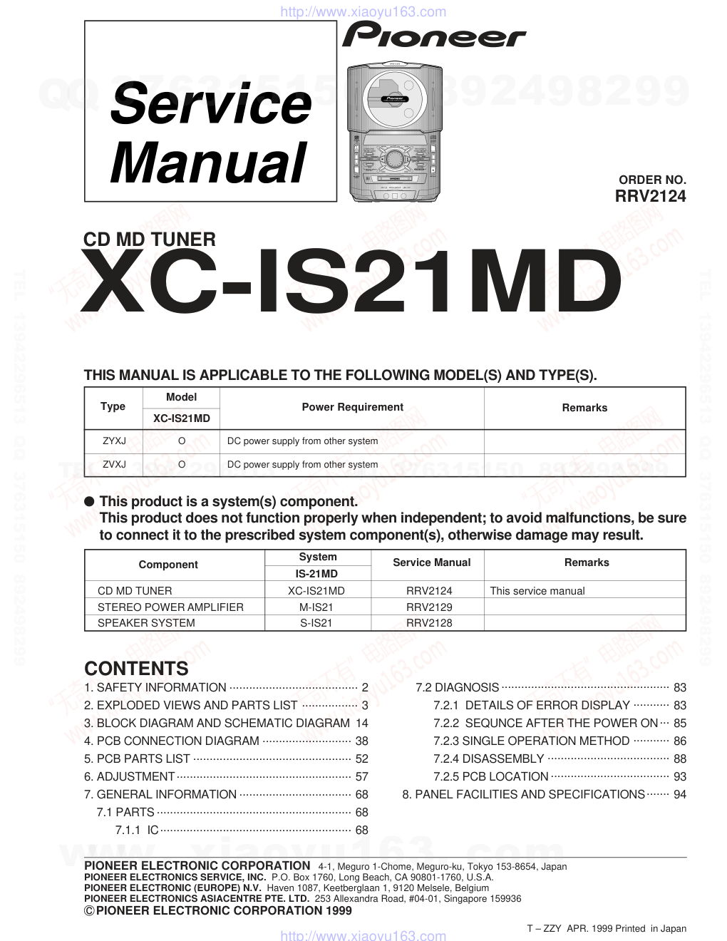 "先锋PIONEER XC-IS21MD电路图-0")
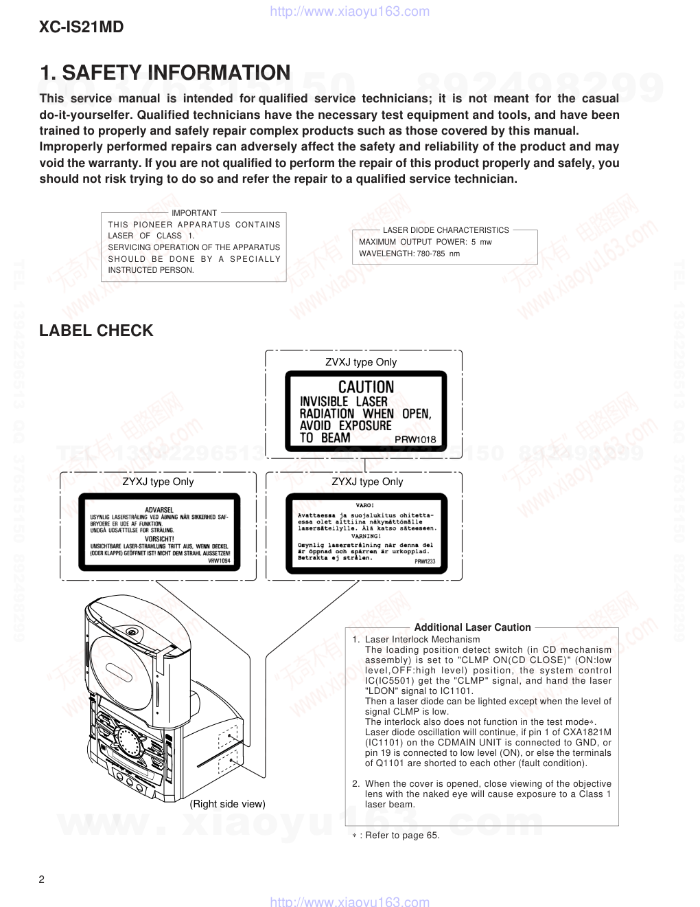 "先锋PIONEER XC-IS21MD电路图-1")
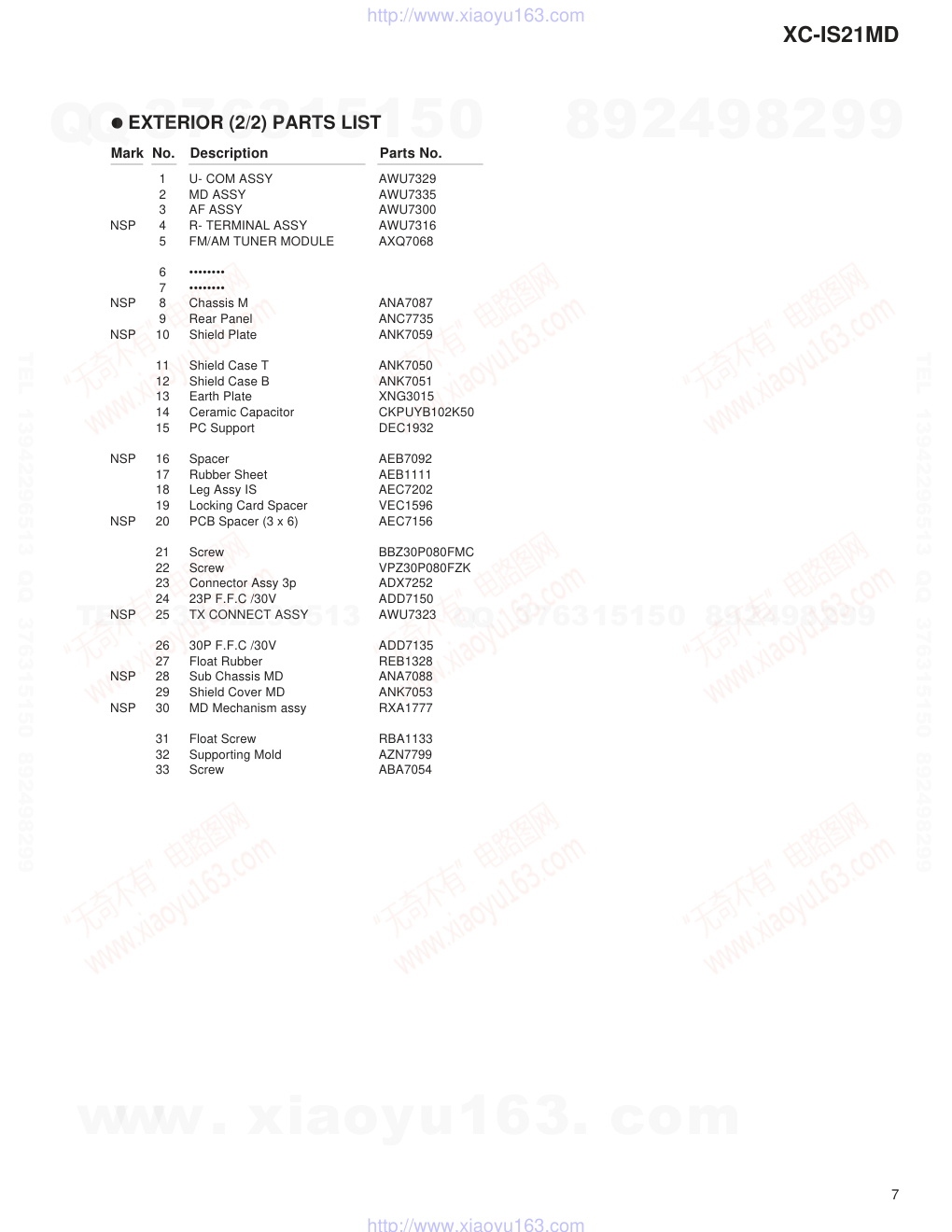
 "先锋PIONEER XC-IS21MD电路图-2")
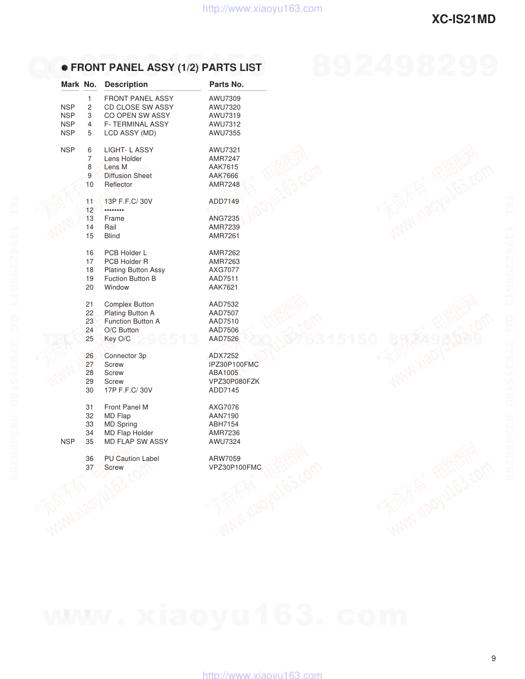
 "先锋PIONEER XC-IS21MD电路图-3")
 "先锋PIONEER XC-IS21MD电路图-4")
 "先锋PIONEER XC-IS21MD电路图-5")
 "先锋PIONEER XC-IS21MD电路图-6")
 "先锋PIONEER XC-IS21MD电路图-7")
 "先锋PIONEER XC-IS21MD电路图-8")
 "先锋PIONEER XC-IS21MD电路图-9")
ORDER NO. PIONEER ELECTRONIC CORPORATION 4-1, Meguro 1-Chome, Meguro-ku, Tokyo 153-8654, Japan PIONEER ELECTRONICS SERVICE, INC. P.O. Box 1760, Long Beach, CA 90801-1760, U.S.A. PIONEER ELECTRONIC (EUROPE) N.V. Haven 1087, Keetberglaan 1, 9120 Melsele, Belgium PIONEER ELECTRONICS ASIACENTRE PTE. LTD. 253 Allexandra Road, #04-01, Singapore 159936 � � � � � � � � � �PIONEER ELECTRONIC CORPORATION 1999 c RRV2124 XC-IS21MD 1. SAFETY INFORMATION ....................................... 2 2. EXPLODED VIEWS AND PARTS LIST ................. 3 3. BLOCK DIAGRAM AND SCHEMATIC DIAGRAM 14 4. PCB CONNECTION DIAGRAM ........................... 38 5. PCB PARTS LIST ................................................ 52 6. ADJUSTMENT..................................................... 57 7. GENERAL INFORMATION .................................. 68 7.1 PARTS ........................................................... 68 7.1.1 IC.......................................................... 68 CONTENTS 7.2 DIAGNOSIS ................................................... 83 7.2.1 DETAILS OF ERROR DISPLAY ........... 83 7.2.2 SEQUNCE AFTER THE POWER ON... 85 7.2.3 SINGLE OPERATION METHOD ........... 86 7.2.4 DISASSEMBLY ..................................... 88 7.2.5 PCB LOCATION .................................... 93 8. PANEL FACILITIES AND SPECIFICATIONS....... 94 T – ZZY APR. 1999 Printed in Japan THIS MANUAL IS APPLICABLE TO THE FOLLOWING MODEL(S) AND TYPE(S). CD MD TUNER Remarks Type Model XC-IS21MD Power Requirement ZYXJ O DC power supply from other system ZVXJ O DC power supply from other system This product is a system(s) component. This product does not function properly when independent; to avoid malfunctions, be sure to connect it to the prescribed system component(s), otherwise damage may result. CD MD TUNER XC-IS21MD RRV2124 This service manual STEREO POWER AMPLIFIER M-IS21 RRV2129 SPEAKER SYSTEM S-IS21 RRV2128 System IS-21MD Component Service Manual Remarks www. xiaoyu163. com QQ 376315150 9 9 2 8 9 4 2 9 8 TEL 13942296513 9 9 2 8 9 4 2 9 8 0 5 1 5 1 3 6 7 3 Q Q TEL 13942296513 QQ 376315150 892498299 TEL 13942296513 QQ 376315150 892498299 http://www.xiaoyu163.com XC-IS21MD 2 1. SAFETY INFORMATION This service manual is intended for qualified service technicians; it is not meant for the casual do-it-yourselfer. Qualified technicians have the necessary test equipment and tools, and have been trained to properly and safely repair complex products such as those covered by this manual. Improperly performed repairs can adversely affect the safety and reliability of the product and may void the warranty. If you are not qualified to perform the repair of this product properly and safely, you should not risk trying to do so and refer the repair to a qualified service technician. IMPORTANT THIS PIONEER APPARATUS CONTAINS LASER OF CLASS 1. SERVICING OPERATION OF THE APPARATUS SHOULD BE DONE BY A SPECIALLY INSTRUCTED PERSON. LASER DIODE CHARACTERISTICS MAXIMUM OUTPUT POWER: 5 mw WAVELENGTH: 780-785 nm LABEL CHECK 1. Laser Interlock Mechanism The loading position detect switch (in CD mechanism assembly) is set to "CLMP ON(CD CLOSE)" (ON:low level,OFF:high level) position, the system control IC(IC5501) get the "CLMP" signal, and hand the laser "LDON" signal to IC1101. Then a laser diode can be lighted except when the level of signal CLMP is low. The interlock also does not function in the test mode∗. Laser diode oscillation will continue, if pin 1 of CXA1821M (IC1101) on the CDMAIN UNIT is connected to GND, or pin 19 is connected to low level (ON), or else the terminals of Q1101 are shorted to each other (fault condition). 2. When the cover is opened, close viewing of the objective lens with the naked eye will cause exposure to a Class 1 laser beam. ∗ : Refer to page 65. Additional Laser Caution ZYXJ type Only ZYXJ type Only ZVXJ type Only (Right side view) www. xiaoyu163. com QQ 376315150 9 9 2 8 9 4 2 9 8 TEL 13942296513 9 9 2 8 9 4 2 9 8 0 5 1 5 1 3 6 7 3 Q Q TEL 13942296513 QQ 376315150 892498299 TEL 13942296513 QQ 376315150 892498299 http://www.xiaoyu163.com 3 XC-IS21MD 2.1 PACKING 2. EXPLODED VIEWS and PARTS LIST NOTES: • Parts marked by "NSP" are generally unavailable because they are not in our Master Spare Parts List. • The mark found on some component parts indicates the importance of the safety factor of the part. Therefore, when replacing, be sure to use parts of identical designation. • Screws adjacent to mark on the product are used for disassembly. (2) CONTRAST TABLE XC-IS21MD/ZYXJ and ZVXJ are constructed the same except for the following: Mark ZYXJ type ZVXJ type 3 Operating Instructions ARC7255 Not used (Spanish/Portuguese/Swedish/Dutch) 4 Operating Instructions ARE7225 Not used (English/French/German/Italian) 5 Operating Instructions Not used ARB7197 (English) NSP 6 Errata ARX7027 ARX7028 12 Power Cord XDG3001 ADG1156 14 Polyethylene Bag Not used Z21-013 (0.05 x 115 x 270) Part No. Remarks Symbol and Description No. 9 10 13 13 12 2 8 11 19 1 16 15 12 5 4 3 6 7 14 17 18 ZVXJ type Only ZYXJ type Only (1) PACKING PARTS LIST Mark No. Description Part No. 1 System Cable ADE7039 2 FM Antenna ADH7005 3 Operating Instructions See Contrast table (2) (Spanish/Portuguese/Swedish/Dutch) 4 Operating Instructions See Contrast table (2) (English/French/German/Italian) 5 Operating Instructions See Contrast table (2) (English) NSP 6 Errata See Contrast table (2) NSP 7 Warranty Card ARY7022 8 AM Loop Antenna ATB7007 9 Remote Control Unit AXD7223 (CU-XR055) 10 RCA Pin- plug Stereo Cable VDE1052 (L= 1.5m) NSP 11 Dry Cell Batteries(AA/R6) VEM-013 12 Power Cord See Contrast table (2) 13 Polyethylene Bag Z21-038 (0.03 x 230 x 340) 14 Polyethylene Bag See Contrast table (2) (0.05 x 115 x 270) 15 Side Pad ML AHA7240 16 Side Pad MR AHA7241 17 Packing Sheet AHG7053 18 Packing Case AHD7754 19 Battery Cover AZA7331 www. xiaoyu163. com QQ 376315150 9 9 2 8 9 4 2 9 8 TEL 13942296513 9 9 2 8 9 4 2 9 8 0 5 1 5 1 3 6 7 3 Q Q TEL 13942296513 QQ 376315150 892498299 TEL 13942296513 QQ 376315150 892498299 http://www.xiaoyu163.com 4 XC-IS21MD 2.2 CD MECHANISM ASSY 2 5 3 10 1 4 7 8 6 9 1 KSS-62A(RP) 8-820-063-(03) 2 Sled Screw Assy X-2646-389-(1) 3 Sled Motor Assy A-4912-199-(A) 4 MD Assy X-2646-482-(1) 5 Geer BN 2-627-761-(02) 6 Rack Spring 2-646-912-(1) 7 Holder 2-648-913-(1) 8 Tapping Screw 2-646-352-01 9 Precision Screw 2-627-668-01 10 Tapping Screw 2-646-358-11 ÷ CD MECHANISM ASSY PARTS LIST Mark No. Description Parts No. www. xiaoyu163. com QQ 376315150 9 9 2 8 9 4 2 9 8 TEL 13942296513 9 9 2 8 9 4 2 9 8 0 5 1 5 1 3 6 7 3 Q Q TEL 13942296513 QQ 376315150 892498299 TEL 13942296513 QQ 376315150 892498299 http://www.xiaoyu163.com 5 XC-IS21MD 1 Rear Cover AMC7029 2 Cussion Rubber AEB7154 3 Jack Door AAN7188 4 Jog Lens AAK7651 5 Jog Knob AAA7005 6 •••••••• 7 •••••••• 8 Jog Escutcheon AAK7620 9 Screw BBZ30P080FMC 10 Screw VPZ30P100FMC (1) EXTERIOR (1/2) PARTS LIST Mark No. Description Parts No. (2) CONTRAST TABLE XC-IS21MD/ZYXJ and ZVXJ are constructed the same except for the following: Mark ZYXJ type ZVXJ type NSP 12 Name Lable AAL7232 AAL7233 13 Coution Label PRW1233 PRW1018 14 Coution Label VRW1094 Not used Part No. Remarks Symbol and Description No. 10 12 9 9 5 8 4 8 3 2 10 10 9 2 11 1 Refer to "2.5 FRONT PANAEL ASSY (1/2) and 2.6 FRONT PANEL ASSY (2/2)" 13 14 ZYXJ type Only 11 Screw BMZ30P060FZK NSP 12 Name Label See Contrast table (2) 13 Caution Label See Contrast table (2) 14 Caution Label See Contrast table (2) Mark No. Description Parts No. 2.3 EXTERIOR (1/2) www. xiaoyu163. com QQ 376315150 9 9 2 8 9 4 2 9 8 TEL 13942296513 9 9 2 8 9 4 2 9 8 0 5 1 5 1 3 6 7 3 Q Q TEL 13942296513 QQ 376315150 892498299 TEL 13942296513 QQ 376315150 892498299 http://www.xiaoyu163.com 6 XC-IS21MD 2.4 EXTERIOR (2/2) 22 23 21 19 9 4 24 22 20 10 22 15 3 21 18 25 17 16 14 13 11 5 12 8 32 32 28 30 26 29 21 2 21 33 27 31 27 21 31 27 1 21 Refer to " 2.7 MD MECHANISM ASSY " Note 1 Cutting Position (No.32 (Supporting Mold) Note 1 Note 1 Cutting Cutting No.32 Rear Corver 21 A A www. xiaoyu163. com QQ 376315150 9 9 2 8 9 4 2 9 8 TEL 13942296513 9 9 2 8 9 4 2 9 8 0 5 1 5 1 3 6 7 3 Q Q TEL 13942296513 QQ 376315150 892498299 TEL 13942296513 QQ 376315150 892498299 http://www.xiaoyu163.com 7 XC-IS21MD 1 U- COM ASSY AWU7329 2 MD ASSY AWU7335 3 AF ASSY AWU7300 NSP 4 R- TERMINAL ASSY AWU7316 5 FM/AM TUNER MODULE AXQ7068 6 •••••••• 7 •••••••• NSP 8 Chassis M ANA7087 9 Rear Panel ANC7735 NSP 10 Shield Plate ANK7059 11 Shield Case T ANK7050 12 Shield Case B ANK7051 13 Earth Plate XNG3015 14 Ceramic Capacitor CKPUYB102K50 15 PC Support DEC1932 NSP 16 Spacer AEB7092 17 Rubber Sheet AEB1111 18 Leg Assy IS AEC7202 19 Locking Card Spacer VEC1596 NSP 20 PCB Spacer (3 x 6) AEC7156 21 Screw BBZ30P080FMC 22 Screw VPZ30P080FZK 23 Connector Assy 3p ADX7252 24 23P F.F.C /30V ADD7150 NSP 25 TX CONNECT ASSY AWU7323 26 30P F.F.C /30V ADD7135 27 Float Rubber REB1328 NSP 28 Sub Chassis MD ANA7088 29 Shield Cover MD ANK7053 NSP 30 MD Mechanism assy RXA1777 31 Float Screw RBA1133 32 Supporting Mold AZN7799 33 Screw ABA7054 ÷ EXTERIOR (2/2) PARTS LIST Mark No. Description Parts No. www. xiaoyu163. com QQ 376315150 9 9 2 8 9 4 2 9 8 TEL 13942296513 9 9 2 8 9 4 2 9 8 0 5 1 5 1 3 6 7 3 Q Q TEL 13942296513 QQ 376315150 892498299 TEL 13942296513 QQ 376315150 892498299 http://www.xiaoyu163.com 8 XC-IS21MD 7 8 9 11 5 6 10 29 26 25 30 24 16 10 18 29 19 29 27 27 15 15 37 29 17 29 29 21 20 29 35 31 28 23 32 34 33 22 2 4 3 1 13 14 13 14 36 2.5 FRONT PANEL ASSY (1/2) www. xiaoyu163. com QQ 376315150 9 9 2 8 9 4 2 9 8 TEL 13942296513 9 9 2 8 9 4 2 9 8 0 5 1 5 1 3 6 7 3 Q Q TEL 13942296513 QQ 376315150 892498299 TEL 13942296513 QQ 376315150 892498299 http://www.xiaoyu163.com 9 XC-IS21MD 1 FRONT PANEL ASSY AWU7309 NSP 2 CD CLOSE SW ASSY AWU7320 NSP 3 CO OPEN SW ASSY AWU7319 NSP 4 F- TERMINAL ASSY AWU7312 NSP 5 LCD ASSY (MD) AWU7355 NSP 6 LIGHT- L ASSY AWU7321 7 Lens Holder AMR7247 8 Lens M AAK7615 9 Diffusion Sheet AAK7666 10 Reflector AMR7248 11 13P F.F.C/ 30V ADD7149 12 •••••••• 13 Frame ANG7235 14 Rail AMR7239 15 Blind AMR7261 16 PCB Holder L AMR7262 17 PCB Holder R AMR7263 18 Plating Button Assy AXG7077 19 Fuction Button B AAD7511 20 Window AAK7621 21 Complex Button AAD7532 22 Plating Button A AAD7507 23 Function Button A AAD7510 24 O/C Button AAD7506 25 Key O/C AAD7526 26 Connector 3p ADX7252 27 Screw IPZ30P100FMC 28 Screw ABA1005 29 Screw VPZ30P080FZK 30 17P F.F.C/ 30V ADD7145 31 Front Panel M AXG7076 32 MD Flap AAN7190 33 MD Spring ABH7154 34 MD Flap Holder AMR7236 NSP 35 MD FLAP SW ASSY AWU7324 36 PU Caution Label ARW7059 37 Screw VPZ30P100FMC ÷ FRONT PANEL ASSY (1/2) PARTS LIST Mark No. Description Parts No. www. xiaoyu163. com QQ 376315150 9 9 2 8 9 4 2 9 8 TEL 13942296513 9 9 2 8 9 4 2 9 8 0 5 1 5 1 3 6 7 3 Q Q TEL 13942296513 QQ 376315150 892498299 TEL 13942296513 QQ 376315150 892498299 http://www.xiaoyu163.com 10 XC-IS21MD B C A 20 27 27 21 21 12 25 13 (1/2) 11 25 24 6 5 9 10 23 8 7 2 17 21 19 18 26 12 25 13 (2/2) 3 22 1 16 15 14 4 Note 1 Cutting Position (No.13 (Mecha Holder) Cutting Note 1 Note 1 No.13 (2/2) No.13 (1/2) Refer to " 2.2 CD MECHANISM ASSY " 2.6 FRONT PANEL ASSY (2/2) www. xiaoyu163. com QQ 376315150 9 9 2 8 9 4 2 9 8 TEL 13942296513 9 9 2 8 9 4 2 9 8 0 5 1 5 1 3 6 7 3 Q Q TEL 13942296513 QQ 376315150 892498299 TEL 13942296513 QQ 376315150 892498299 http://www.xiaoyu163.com 11 XC-IS21MD 1 CD MOTOR ASSY AWU7318 2 CD ASSY AWU7306 3 Slider Motor VXM1033 NSP 4 Motor Shield ANK7067 5 Motor Pulley PNW1634 6 Gear Holder AMR7240 7 Gear A ANW7063 8 Gear B AMR7260 9 Gear Pulley A ANW7066 10 Belt AEB7171 11 CD MECHANISM ASSY KSM-620AAA 12 Float Spring ABH7170 13 Mechanism Holder AMR7242 14 CD Door Window AAK7673 15 CD Door Escutcheon AAK7619 16 CD Door AAN7189 17 Shaft Assy AXG7078 18 Shaft Holder AMR7237 19 Cussion Rubber AEB7154 20 Screw BBZ30P080FMC 21 Screw VPZ30P080FZK 22 Screw ABA7054 23 Screw PMZ26P040FMC 24 Screw IPZ20P080FMC 25 Float Rubber AEB7129 26 17P F.F.C/ 30V ADD7146 27 Screw VPZ30P100FMC ÷ FRONT PANEL ASSY (2/2) PARTS LIST Mark No. Description Parts No. www. xiaoyu163. com QQ 376315150 9 9 2 8 9 4 2 9 8 TEL 13942296513 9 9 2 8 9 4 2 9 8 0 5 1 5 1 3 6 7 3 Q Q TEL 13942296513 QQ 376315150 892498299 TEL 13942296513 QQ 376315150 892498299 http://www.xiaoyu163.com 12 XC-IS21MD 2.7 MD MECHANISM ASSY 49 48 40 42 38 43 40 33 44 31 28 32 34 40 11 5 10 17 6 4 9 54 19 21 20 18 37 16 26 15 13 14 37 12 53 52 51 A E E F F G G H A B B C C D D 37 8 40 24 25 39 27 41 35 36 29 39 46 23 30 45 2 3 50 47 54 CN103 CN101 CN102 CN105 1 H www. xiaoyu163. com QQ 376315150 9 9 2 8 9 4 2 9 8 TEL 13942296513 9 9 2 8 9 4 2 9 8 0 5 1 5 1 3 6 7 3 Q Q TEL 13942296513 QQ 376315150 892498299 TEL 13942296513 QQ 376315150 892498299 http://www.xiaoyu163.com 13 XC-IS21MD • MD MECHANISM ASSY PARTS LIST Mark No. Description Part No. Mark No. Description Part No. 1 CORE MAIN UNIT ASSY RWZ4334 NSP 2 CORE SW UNIT ASSY RWZ4335 3 Lead Card 7P RDD1403 4 Lead Wire RKP1814 5 Lever Spring RBH1463 6 Clamp Spring 1 RBK1074 7 •••••••• 8 Loading Belt REB1329 9 Lock Plate RNE1949 10 Loading Base RNK2323 11 Under Slider RNK2314 12 Gear Pulley RNK2316 13 Drive Gear RNK2317 14 Clutch Gear RNK2318 15 Flip Disk RNK2319 16 SW Lever RNK2320 17 Shutter Assy RXA1774 NSP 18 Upper Slider Assy RXA1782 19 Eject Spring RBH1461 20 Upper Slider RNK2324 21 Carrier RNK2315 22 •••••••• 23 Spindle Spring RBH1460 24 Lifter Spring RBH1462 25 Screw Guide RBK1072 26 S. H. Spring RBK1073 27 Guide Shaft RLA1312 28 Lead Screw RLA1311 29 Shield Case RNE1950 30 Reference Plate RNK2306 31 S. Holder RNK2307 32 Worm Wheel RNK2309 33 Hook RNK2310 34 Head Lifter RNK2311 35 MD Head RPB1063 36 MD Pick-up RWY1019 37 Screw Z39-019 38 Screw JFZ17P020FZK 39 Screw JGZ14P020FMC 40 Screw JGZ17P028FMC 41 Screw JGZ17P040FMC 42 Screw PMB20P040FMC 43 Servo Base Assy REA1283 NSP 44 Clamp Magnet RMF1002 NSP 45 Servo Base RNE1951 NSP 46 Disc Table RNK2305 NSP 47 Spindle Motor RXM1091 48 Carriage Motor Assy REA1284 49 Worm RNK2308 NSP 50 Carriage Motor RXM1090 51 Loading Motor Assy REA1290 52 DC Motor /0.75W PXM1010 53 CA Pulley RNK2322 54 Screw BPZ20P080FMC www. xiaoyu163. com QQ 376315150 9 9 2 8 9 4 2 9 8 TEL 13942296513 9 9 2 8 9 4 2 9 8 0 5 1 5 1 3 6 7 3 Q Q TEL 13942296513 QQ 376315150 892498299 TEL 13942296513 QQ 376315150 892498299 http://www.xiaoyu163.com XC-IS21MD 14 A B C D 1 2 3 4 1 2 3 4 3. BLOCK DIAGRAM and SCHEMATIC DIAGRAM 3.1 BLOCK DIAGRAM RF–AMP (IC101) IR3R55M TUNER MODULE TX CONNECT ASSY FRONT PANEL ASSY CN6201 CN161 A B M TX LcH KEY JOG TX LcH KEY 1 JOG KEY 2 KEY 3 TX+5V TX+5V U-COM ASSY LCD ASSY J60 J160 C CD ASSY F CORE SW ASSY CORE MAIN ASSY K J D TX LcH TX+5V (CD) (TX) (TX) (TX) (TX) (FS) (TS) (TS) IC1101 CXA1821M IC1201 CXD2587Q IC5501 PDG241 IC1301 BA5970FP (D.O) (FS) (SM) (CM) (CM) (TS) (TS) (TS) (FS) (FS) (TS) (FS) (FS) (SM) (FS) (FS) (TS) (TS) (SM) (SM) (CS) (CS) CD L D. OUT D. OUT CD LD ON LCD_CE LCD_CLK LCD_DATA LCD_CE LCD_CLK LCD_DATA CN10 CN40 CN110 V+5UN V+5UN J101 V+5CDM V+5CDM GNDCDM V+5CD V+5CD TFDR TRDR FFDR FRDR TFDR TRDR FFDR FRDR GND GND GND V+5CD V+5CD GNDCDM V+12TX GNDU GNDU AC SYSTEM U-COM 13 65 66 67 79 80 81 44 AC_PLUS 60 44 38 39 40 11 47 10 46 9 CN150 CN50 17 CN70 CN105 CN105 Q5501 V+12TX V+5.6U V+5.6U PICKUP ASSY INSIDE SW (S701) 13 16 17 21 25–28 DRIVER (IC106) M56758FP HEAD DRIVER (IC116) BD7910FV 13 17 15 7 30 31 29 28 35 34 9 12 8 LOAD SW (S101) LOAD SW (S102) DISC SW (S702) 4 3 2 1 ENC/DEC + DIGITAL SERVO (IC102) LR376487 MECHA CONTROL µCOM (IC104) PD5523A 3 50 74 73 40 66 4M–DRAM (IC103) M5M4V4400CTP-7 X'tal (X101) 33.8688MHz 26–29, 32–37, 39–46 1–5, 9–12, 14–18, 22–25 EEP–ROM (IC110) BR93LC56F 3–6 31–33, 55 7 25 24 26 25 6 31 15 16 3 2 23 22 21 20 19 18 37 24 23 27 28 23 1 90 89 20 23 57 59 92 82–86, 89–100 15, 18, 19, 29, 40, 80, 44–54 35 36 34 37 64, 65 DIFFERENTIAL AMP (IC112) BA4510F EFM EFMO EFMI EFMO FODF FODF FODR FODR TRDF TRDR SLDF SLDR TRDF TRDR SLDF SLDR DSCK LD+ SW1 PLOAD RLOAD DISC LD- SPDF DSTB DADATA DIN ADDATA MDDATA SYSDATA SPDR LOADING MOTOR SLED MOTOR (CARRIAGE) REC HEAD SPINDLE MOTOR (REC) (REC) (PB) (PB) MDCLK CDLDON MDODATA MDIDATA MDSTB OPTIN1 OPTIN2 MDCLK MDODATA MDIDATA MDSTB OPTIN1 OPTIN2 VM+5V D+5V 7 1 2 7 2 7 2 7 2 7 6 16 8 15 11 10 9 10 13 15 17 10 13 15 15 14 13 12 3 2 1 15 10 3 4 8 5 7 24 27 30 25 14 17 20 18 11 10 9 8 7 1 M+5V CN104 GND GND D.GND D.GND D.GND D+5V DIN DADATA ADDATA MDDATA SYSDATA XDSCK XDSTB 13 16 17 21 28 27 26 25 1 2 1 2 3 4 5 6 7 CN101 CN103 CN105 1 2 CN102 1 2 3 4 5 6 7 CN701 SL+ SL1 SP- SP+ GNDM GNDM SL+ SL1 SW1 DISC SP- SP+ GNDM SW1 DISC SL+ SL1 SP- SP+ SW1 DISC TP704 SP+ (RED) TP703 SP- (BLACK) TP702 SLD- (BLUE) TP701 SLD+ (ORANGE) HEAD HEAD CD MECHA ASSY LD PD PDIC PD1 PDIC PD2 F E CN1101 LD ON SL + CN1301 SL - SP + SP - VC T + CN1101 F - F + T - PICKUP ASSY (2/2) PICKUP ASSY (1/2) SL SP SL/SP MOTOR + - + - 1 2 3 4 15 8 14 9 12 7 6 1 2 5 6 RF1 RF3 RF4 RF2 F- T+ F+ T- LOAD- LOAD+ www. xiaoyu163. com QQ 376315150 9 9 2 8 9 4 2 9 8 TEL 13942296513 9 9 2 8 9 4 2 9 8 0 5 1 5 1 3 6 7 3 Q Q TEL 13942296513 QQ 376315150 892498299 TEL 13942296513 QQ 376315150 892498299 http://www.xiaoyu163.com XC-IS21MD 15 A B C D 5 6 7 8 5 6 7 8 AF ASSY E MD ASSY L R- TERMINAL ASSY H TX LcH CN5 REC L PB L CD L LIN2 CN3 CN1 AOUT L LIN1 LOUT1 LOUT2 CN32 CN31 CN131 CN7101 CN3 IC141 (NJM7805FA) IC131 (NJM7812FA) IC3001 (LC75398NE) + - IC3002 (NJM4558MD) 3 1 2 (MO) (MO) (MO) (MO) (LO1) (LO1) (LO2) (L1) (L1) (L2) (L2) (L1) (LO) (PB) (PB) (PB) (PB) (CD) (L2) (L2) (CD) (REC) (REC) (REC) (REC) (REC) (REC) (REC) (TX) (L1) (TX) PB L LIN 2 CD L TX L LIN1 AOUT L AUDIO OUT LINE IN1 LIN1 LOUT1 LIN2 LOUT2 CN132 J103 (LO2) F- TERMINAL ASSY I LINE OUT1 LINE OUT2 LINE IN2 OPT OUT D3009 D3008 TX+5V CN1 CN5 D. OUT CN4 CN2 CN4 CD. OUT CN1 CD. OUT LINE DIN CD. OPT IN J104 PB L REC L GND GND V+12V V+12V VD+5V VM+5V VD+5V VM+5V J102 J104 V+5UN V+12TX GNDU V+5CDM V+5CD GNDCDM V+5UN AC V+5.6U GNDS GNDS V+12UN V+12UN V+12UN 1 AC AC AC 3 V+5.6V V+5.6V V+5.6V 4 B2GND B1GND GNDU B2GND B1GND GNDU V+5UN 5 B2GND 6 B1GND 9 GNDU 10 V+5UN V IN VCC GND OPT OPT IN/OUT V+5 OPT GND OPT TO. STEREO PWER AMPLIFIER (M-IS21) V+12V IC4001 (NJM7805FA) VD+5V VM+5V VH+5V V+5 SIGNAL ROUTE : CD AUDIO SIGNAL : LINE 1 SIGNAL : MD PB SIGNAL : LINE 2 SIGNAL : MAIN OUT SIGNAL : OPTICAL OUT SIGNAL (L1) (CD) (PB) (L2) (MO) (D.O) (TX) (LO1) (LO2) (LO) (REC) : TUNER AUDIO SIGNAL : LINE OUT 1 SIGNAL : LINE OUT 2 SIGNAL : LINE OUT SIGNAL : RECORDING SIGNAL 1 2 3 V+5 (D.O) (D.O) (D.O) (D.O) (D.O) (D.O) (D.O) (D.O) DIN CN4101 GND VM+5V GND D.GND D.GND MOD DATA J140 MD CLK OPT2 OPT1 DSTB MDI DATA DA DATA DA DATA AD DATA AD DATA DSCK DSTB MD DATA SYS DATA D GND VH+5V IC4301 (AK4520A) IC4801 (TC74HC00AF) IC4202 (BA4558F) (PB) VD+5V VH+5V VD+5V VA+5V VD+3V VM+5V VA+5V + + VD+5V VM+5V VA+12V V+12V VM+5V VD+5V Q4002 2SD1858X Q4003 2SC1740S D4004 D4003 VD+3V VA+12V VH+5V VH+5V VH+5V VH+5V 7 9 8 10 3 2 6 7 9 8 10 3 2 6 6 7 9 12 6 7 9 12 2 8 9 7 1 1 8 9 7 3 4 2 3 4 2 4 3 7 5 4 3 7 5 9 10 9 7 10 2 10 5 18 8 16 9 3 4 8 17 23 2 1 15 14 13 3 24 27 30 25 14 17 20 18 11 10 9 8 7 1 SIGNAL ROUTE : FOCUS SERVO LOOP LINE : TRACKING SERVO LOOP LINE (FS) (TS) : SPINDLE MOTOR ROUTE : CARRIAGE MOTOR ROUTE : LOADING MOTOR ROUTE (SM) (LM) (CM) www. xiaoyu163. com QQ 376315150 9 9 2 8 9 4 2 9 8 TEL 13942296513 9 9 2 8 9 4 2 9 8 0 5 1 5 1 3 6 7 3 Q Q TEL 13942296513 QQ 376315150 892498299 TEL 13942296513 QQ 376315150 892498299 http://www.xiaoyu163.com XC-IS21MD 16 A B C D 1 2 3 4 1 2 3 4 3.2 OVERALL CONNECTION DIAGRAM AF ASSY (AWU7300) CD MOTOR ASSY (AWU7318) E G F-TERMINAL ASSY (AWU7312) I CD ASSY (AWU7306) F LCD ASSY (AWU7355) D TUNER MODULE (AXQ7068) MD ASSY (AWU7335) TX CONNECT ASSY (AWU7323) A L CORE MAIN ASSY (RWZ4334) MD MECHANISM ASSY (AXA7077) J CORE SW ASSY (RWZ4335) K B CN2 CN4 CN1 J101 CN40 J60 J160 CN161 CN6201 CN110 CN10 CN70 CN1101 CN1301 J111 CN11 CN3 J103 CN7 J107 CN170 CN104 J102 J104 J140 CN4101 www. xiaoyu163. com QQ 376315150 9 9 2 8 9 4 2 9 8 TEL 13942296513 9 9 2 8 9 4 2 9 8 0 5 1 5 1 3 6 7 3 Q Q TEL 13942296513 QQ 376315150 892498299 TEL 13942296513 QQ 376315150 892498299 http://www.xiaoyu163.com XC-IS21MD 17 A B C D 5 6 7 8 5 6 7 8 Note : When ordering service parts, be sure to refer to "EXPLODED VIEWS and PARTS LIST" or "PCB PARTS LIST". U- COM ASSY (AWU7329) C R-TERMINAL ASSY (AWU7316) H FRONT PANEL ASSY (AWU7309) CD CLOSE SW ASSY (AWU7320) M P CD OPEN SW ASSY (AWU7319) LIGHT-L ASSY (AWU7321) O N MD FLAP ASSY (AWU7324) Q CN5 CN105 CN32 CN132 CN131 CN31 J55 J155 J54 J154 J152 CN51 J52 J51 CN150 CN50 www. xiaoyu163. com QQ 376315150 9 9 2 8 9 4 2 9 8 TEL 13942296513 9 9 2 8 9 4 2 9 8 0 5 1 5 1 3 6 7 3 Q Q TEL 13942296513 QQ 376315150 892498299 TEL 13942296513 QQ 376315150 892498299 http://www.xiaoyu163.com XC-IS21MD 18 A B C D 1 2 3 4 1 2 3 4 3.3 TUNER ASSY (FM) (FM) (FM) (AM) (AM) (AM) (AM) (AM) (FM) (FM) (FM) (FM) (FM) (FM) (FM) (FM) : AM SIGNAL ROUTE : FM SIGNAL ROUTE : TUNER AUDIO SIGNAL (AM) (FM) (TX) FM/AM TUNER MODULE (AXQ7068) A RF AMP MIX AMP BUFFER IF AMP PLL FM +B SW AM RF TUNING BLOCK OSC A www. xiaoyu163. com QQ 376315150 9 9 2 8 9 4 2 9 8 TEL 13942296513 9 9 2 8 9 4 2 9 8 0 5 1 5 1 3 6 7 3 Q Q TEL 13942296513 QQ 376315150 892498299 TEL 13942296513 QQ 376315150 892498299 http://www.xiaoyu163.com XC-IS21MD 19 A B C D 5 6 7 8 5 6 7 8 (FM) (AM) (AM) (AM) (FM) (TX) (TX) (TX) J60 CN6201 CN161 J160 D20PYY1315 TX CONNECT ASSY (AWU7323) B AF AMP REGULATOR AF AMP C B A www. xiaoyu163. com QQ 376315150 9 9 2 8 9 4 2 9 8 TEL 13942296513 9 9 2 8 9 4 2 9 8 0 5 1 5 1 3 6 7 3 Q Q TEL 13942296513 QQ 376315150 892498299 TEL 13942296513 QQ 376315150 892498299 http://www.xiaoyu163.com XC-IS21MD 20 A B C D 1 2 3 4 1 2 3 4 3.4 U-COM ASSY U-COM ASSY (AWU7329) C M CN150 E CN5 CN50 CN105 B J160 J60 SIGNAL ROUTE : TUNER AUDIO SIGNAL (TX) (TX) (TX) (TX) C www. xiaoyu163. com QQ 376315150 9 9 2 8 9 4 2 9 8 TEL 13942296513 9 9 2 8 9 4 2 9 8 0 5 1 5 1 3 6 7 3 Q Q TEL 13942296513 QQ 376315150 892498299 TEL 13942296513 QQ 376315150 892498299 http://www.xiaoyu163.com XC-IS21MD 21 A B C D 5 6 7 8 5 6 7 8 CN10 CN40 CN70 CN170 LCD ASSY (AWU7355) D F CN110 L J140 0.47/50 PDG241B D C www. xiaoyu163. com QQ 376315150 9 9 2 8 9 4 2 9 8 TEL 13942296513 9 9 2 8 9 4 2 9 8 0 5 1 5 1 3 6 7 3 Q Q TEL 13942296513 QQ 376315150 892498299 TEL 13942296513 QQ 376315150 892498299 http://www.xiaoyu163.com XC-IS21MD 22 A B C D 1 2 3 4 1 2 3 4 3.5 AF ASSY AF ASSY (AWU7300) E F J101 L J102 L J104 CN1 CN2 CN4 C CN105 CN5 CN7 J107 CD TOUCH SIGNAL ROUTE : CD AUDIO SIGNAL : LINE 1 SIGNAL : PB SIGNAL : LINE 2 SIGNAL : MAIN OUT SIGNAL (L1) (CD) (PB) (L2) (MO) (TX) (LO1) (LO2) (LO) (REC) : TUNER AUDIO SIGNAL : LINE OUT 1 SIGNAL : LINE OUT 2 SIGNAL : LINE OUT SIGNAL : RECORDING SIGNAL (MO) (LO) (LO) (L2) (L2) (L1) (L1) (PB) (CD) (CD) (CD) (L1) (L1) (L2) (TX) (TX) (TX) (TX) (TX) (TX) (PB) (REC) (REC) (REC) (REC) (REC) (PB) (PB) (PB) E www. xiaoyu163. com QQ 376315150 9 9 2 8 9 4 2 9 8 TEL 13942296513 9 9 2 8 9 4 2 9 8 0 5 1 5 1 3 6 7 3 Q Q TEL 13942296513 QQ 376315150 892498299 TEL 13942296513 QQ 376315150 892498299 http://www.xiaoyu163.com XC-IS21MD 23 A B C D 5 6 7 8 5 6 7 8 H CN132 H CN131 CN31 CN32 I J103 CN3 (MO) (LO1) (LO1) (MO) (MO) (MO) (LO1) (LO1) (LO) (LO2) (LO2) (L2) (L2) (L1) (L1) (L1) (L1) (L1) 390 390 390 S5688G S5688G E www. xiaoyu163. com QQ 376315150 9 9 2 8 9 4 2 9 8 TEL 13942296513 9 9 2 8 9 4 2 9 8 0 5 1 5 1 3 6 7 3 Q Q TEL 13942296513 QQ 376315150 892498299 TEL 13942296513 QQ 376315150 892498299 http://www.xiaoyu163.com XC-IS21MD 24 A B C D 1 2 3 4 1 2 3 4 3.6 CD ASSY CD ASSY (AWU7300) F To. CD MECHA To. P.U Assy CN1301 CN1101 1 1 2 VC IC1101- Pin 16: PLAY MODE (RF) 1.0Vp-p 2 IC1101- Pin 13 : TEST MODE, Tracking Open (TRER) H : 500nsec/div H : 5msec/div VC : IC1101- Pin12 VC 1.0Vp-p Note: The encircled numbers denote measuring point in the schematic diagram. VC SIGNAL ROUTE : CD AUDIO SIGNAL ROUTE : FOCUS SERVO LOOP LINE : TRACKING SERVO LOOP LINE (FS) (TS) : SPINDLE MOTOR ROUTE : CARRIAGE MOTOR ROUTE : LOADING MOTOR ROUTE (SM) (LM) (CM) (FS) (TS) (FS) (TS) (SM) (SM) (TS) (LM) (LM) (SM) (SM) (FS) (FS) (TS) (CM) (CM) (TS) (TS) (FS) (FS) (FS) (SM) (SM) (CM) (CM) (FS) (TS) (TS) F www. xiaoyu163. com QQ 376315150 9 9 2 8 9 4 2 9 8 TEL 13942296513 9 9 2 8 9 4 2 9 8 0 5 1 5 1 3 6 7 3 Q Q TEL 13942296513 QQ 376315150 892498299 TEL 13942296513 QQ 376315150 892498299 http://www.xiaoyu163.com XC-IS21MD 25 A B C D 5 6 7 8 5 6 7 8 CD MOTOR ASSY (AWU7318) G J101 CN110 C CN10 CN1 E J111 CN11 (FS) (TS) (SM) (CM) (CM) (TS) (TS) (FS) (FS) G F www. xiaoyu163. com QQ 376315150 9 9 2 8 9 4 2 9 8 TEL 13942296513 9 9 2 8 9 4 2 9 8 0 5 1 5 1 3 6 7 3 Q Q TEL 13942296513 QQ 376315150 892498299 TEL 13942296513 QQ 376315150 892498299 http://www.xiaoyu163.com XC-IS21MD 26 A B C D 1 2 3 4 1 2 3 4 3.7 REAR and FRONT ASSYS R- TERMINAL ASSY (AWU7316) H E CN31 E CN32 CN131 CN132 TO. STEREO POWER AMPLIFIER (M-IS21) TO. OPTION DECK (MO) (MO) (MO) (MO) (LO1) (LO1) (LO1) (L1) (L1) (L1) SIGNAL ROUTE : MAIN OUT SIGNAL : LINE 1 SIGNAL : LINE OUT1 SIGNAL (L1) (LO1) (MO) CN7101 CN7102 H www. xiaoyu163. com QQ 376315150 9 9 2 8 9 4 2 9 8 TEL 13942296513 9 9 2 8 9 4 2 9 8 0 5 1 5 1 3 6 7 3 Q Q TEL 13942296513 QQ 376315150 892498299 TEL 13942296513 QQ 376315150 892498299 http://www.xiaoyu163.com XC-IS21MD 27 A B C D 1 2 3 4 1 2 3 4 F- TERMINAL ASSY (AWU7312) I E CN3 J103 (L2) (L2) (L2) (L2) (LO2) (LO2) (LO2) SIGNAL ROUTE : LINE 2 SIGNAL : LINE OUT2 SIGNAL (LO2) (L2) VTL1105 I www. xiaoyu163. com QQ 376315150 9 9 2 8 9 4 2 9 8 TEL 13942296513 9 9 2 8 9 4 2 9 8 0 5 1 5 1 3 6 7 3 Q Q TEL 13942296513 QQ 376315150 892498299 TEL 13942296513 QQ 376315150 892498299 http://www.xiaoyu163.com XC-IS21MD 28 A B C D 1 2 3 4 1 2 3 4 3.8 CORE MAIN and CORE SW ASSYS PICKUP ASSY (CARRIAGE) CN101 CN102 CN105 CN701 CN103 CORE MAIN ASSY (RWZ4334) J CORE SW ASSY (RWZ4335) K 1 2 10 11 8 9 3 J K www. xiaoyu163. com QQ 376315150 9 9 2 8 9 4 2 9 8 TEL 13942296513 9 9 2 8 9 4 2 9 8 0 5 1 5 1 3 6 7 3 Q Q TEL 13942296513 QQ 376315150 892498299 TEL 13942296513 QQ 376315150 892498299 http://www.xiaoyu163.com XC-IS21MD 29 A B C D 5 6 7 8 5 6 7 8 CN104 L CN4101 : MD PLAYBACK SIGNAL : REC SIGNAL : OUTPUT DIGITAL AUDIO SIGNAL : INPUT DIGITAL AUDIO SIGNAL : RF SIGNAL SIGNAL ROUTE (PB) (PB) (PB) 6 5 4 J www. xiaoyu163. com QQ 376315150 9 9 2 8 9 4 2 9 8 TEL 13942296513 9 9 2 8 9 4 2 9 8 0 5 1 5 1 3 6 7 3 Q Q TEL 13942296513 QQ 376315150 892498299 TEL 13942296513 QQ 376315150 892498299 http://www.xiaoyu163.com XC-IS21MD 30 1.53V 3.18V 1.65V 0V 1.42V 0V 1.59V 1.41V 1.97V 1.39V 1.64V 3.18V 0V 0V 0V 0V 1.69V 1.52V 1.70V 1.47V 1.47V 1.65V 1.54V 1.69V 1.51V 0.82V 2.0V 2.0V 1.81V 1.4V 0.82V 1.67V 1.67V 1.67V 2.86V 1.32V 2.23V 0V 2.4V 1.2V 1.5V 0V 2.0V 3.0V 1.2V 1.2V 0.02V 3.04V 1.57V 0.05V 9 8 7 6 5 4 3 2 1 30 29 28 27 26 25 24 23 22 21 20 19 18 17 16 15 14 13 12 11 10 49 48 47 46 45 44 43 42 41 40 39 38 37 36 35 34 33 32 31 PIN NO. VOLTAGE 50 IC102 1.59V 0V 0V 1.59V 1.8V 0V 0V 0V 0V 0V 0.56V 3.18V 0V 1.5V 1.5V 3.2V 1.6V 3.2V 0V 1.6V 1.6V 1.48V 0V 0V 1.68V 1.82V 1.59V 0.35V 0.02V 3.2V 3.2V 0.02V 0.03V 1.9V 1.56V 3.1V 3.2V 0V 3.19V 0.5V 0.5V 0.5V 0.5V 0.9V 0.5V 0.5V 0.5V 0.8V 3.18V 0.06V 59 58 57 56 55 54 53 52 51 79 78 77 76 75 74 73 72 71 70 69 68 67 66 65 64 63 62 61 60 98 97 96 95 94 93 92 91 90 89 88 87 86 85 84 83 82 81 80 PIN NO. VOLTAGE 99 100 0V 0V 0.22V 0.03V 1.29V 2.21V 3.13V 0V 0V 0V 0V 3.03V 1.43V 0V 1.57V 3.2V 3.19V 3.1V 0.03V 0V 0V 3.18V 3.2V 0V 2.67V 3.19V 0V 0V 2.4V 0.24V 0V 0.3V 3.2V 1.56V 1.0V 0V 2.77V 0V 3.18V 0.02V 3.19V 3.2V 0V 0.05V 3.18V 3.19V 0.51V 0.4V 0.3V 0.55V 9 8 7 6 5 4 3 2 1 30 29 28 27 26 25 24 23 22 21 20 19 18 17 16 15 14 13 12 11 10 49 48 47 46 45 44 43 42 41 40 39 38 37 36 35 34 33 32 31 PIN NO. VOLTAGE 50 IC104 0.54V 0.6V 0.6V 0.6V 0V 0V 0V 0V 3.2V 0V 0V 3.2V 0V 0V 3.2V 0V 0V 0V 0V 0V 0V 3.1V 3.2V 0V 0V 3.2V 0V 0V 0V 3.2V 0V 3.19V 0V 3.19V 0V 3.18V 3.2V 0V 1.03V 1.6V 0.56V 1.49V 1.49V 0.68V 0.61V 0V 0.53V 3.2V 3.2V 0V 59 58 57 56 55 54 53 52 51 79 78 77 76 75 74 73 72 71 70 69 68 67 66 65 64 63 62 61 60 98 97 96 95 94 93 92 91 90 89 88 87 86 85 84 83 82 81 80 PIN NO. VOLTAGE 99 100 0.78V 0.73V 0.77V 0.75V 1.61V 1.61V 0.75V 1.61V 1.61V 1.61V 1.61V 1.61V 3.19V 3.19V 0V 0V 3.19V 0V 0V 1.5V 3.2V 0V 0V 3.19V 2.0V 0V 1.40V 1.42V 1.40V 1.63V 1.61V 1.61V 0V 0V 0V 1.62V 0.59V 1.61V 1.61V 1.61V 1.61V 3.19V 0V 1.08V 1.61V 1.61V 0V 0.74V 9 8 7 6 5 4 3 2 1 30 29 28 27 26 25 24 23 22 21 20 19 18 17 16 15 14 13 12 11 10 42 43 44 45 46 47 48 41 40 39 38 37 36 35 34 33 32 31 VOLTAGE IC101 PIN NO. 1.2V 1.2V 3.0V 2.0V 0V 2.23V 1.32V 2.86V 1.67V 3.18V 1.67V 1.67V 1.67V 2.86V 1.32V 2.23V 2.4V 1.2V 1.5V 0V 9 5 4 3 2 1 26 25 24 23 22 18 17 16 15 14 13 12 11 10 PIN NO. VOLTAGE IC103 Voltages MD CORE MAIN ASSY J www. xiaoyu163. com QQ 376315150 9 9 2 8 9 4 2 9 8 TEL 13942296513 9 9 2 8 9 4 2 9 8 0 5 1 5 1 3 6 7 3 Q Q TEL 13942296513 QQ 376315150 892498299 TEL 13942296513 QQ 376315150 892498299 http://www.xiaoyu163.com XC-IS21MD 31 9 8 7 6 5 4 3 2 1 16 15 14 13 12 11 10 PIN NO. VOLTAGE IC108 2.47V 2.63V 4.87V 2.63V 1.59V 0V 0V 4.87V 0V 2.25V 4.94V 4.94V 4.94V 4.94V 3.12V 4.94V 9 8 7 6 5 4 3 2 1 14 13 12 11 10 PIN NO. VOLTAGE IC109 2.77V 2.77V 3.2V 1.58V 1.58V 1.56V 0V 0V 0V 0V 0V 0V 0V 3.2V 9 8 7 6 5 4 3 2 1 20 19 18 17 16 15 14 13 12 11 10 PIN NO. VOLTAGE IC116 4.98V 0V 0V 4.99V 3.2V 0V 0.03V 3.18V 0V 0V 0V 0.22V 0V 0.25V 0.25V 2.82V 0.16V 4.94V 2.82V 1.33V 1.6V 0.49V 1.61V 4.99V 4.99V 1.61V 1.62V 2.46V 2.51V 0V 0V 2.54V 2.45V 1.62V 1.62V 1.61V 3.17V 0V 1.61V 1.61V 1.61V 1.61V 1.36V 1.36V 1.61V 1.61V 1.63V 2.41V 2.55V 2.47V 2.48V 0V 0V 2.79V 2.18V 0V 1.69V 5.0V 4.99V 1.67V 1.69V 1.69V 9 8 7 6 5 4 3 2 1 30 29 28 27 26 25 24 23 22 21 20 19 18 17 16 15 14 13 12 11 10 42 41 40 39 38 37 36 35 34 33 32 31 VOLTAGE IC106 PIN NO. 1.66V 1.62V 1.62V 0V 1.67V 1.67V 1.67V 3.19V 8 7 6 5 4 3 2 1 PIN NO. VOLTAGE IC112 0V 3.2V 0V 3.2V 0V 0.11V 0V 0V 8 7 6 5 4 3 2 1 PIN NO. VOLTAGE IC110 9 8 7 6 5 4 3 2 1 14 13 12 11 10 PIN NO. VOLTAGE IC113 4.95V 3.96V 0V 0V 0V 0V 0V 0V 4.94V 4.12V 3.19V 0V 0V 4.94V 0V 4.19V 3.21V 2.81V 0V 5 4 3 2 1 PIN NO. VOLTAGE IC114 www. xiaoyu163. com QQ 376315150 9 9 2 8 9 4 2 9 8 TEL 13942296513 9 9 2 8 9 4 2 9 8 0 5 1 5 1 3 6 7 3 Q Q TEL 13942296513 QQ 376315150 892498299 TEL 13942296513 QQ 376315150 892498299 http://www.xiaoyu163.com XC-IS21MD 32 1 –– GND DC500mV/div., 10 µSec/div. IC101-pin35 (ADIPO) MODE: PLAY DISC: GGF1328 (MMD–212) 2 IC101-pin30 (WBO) MODE: PLAY DISC: GGF1328 (MMD–212) –– GND DC1V/div., 10 µSec/div. 3 IC102-pin1 (EFM MON) MODE: PLAY DISC: TGTS1 or MMD–110 –– GND DC500mV/div., 0.5mSec/div. 6 –– GND DC500mV/div., 2mSec/div. IC102-pin77 (TE MON) MODE: PLAY DISC: TGTS1 or MMD–110 7 IC102-pin54 (TES01) MODE: STOP –– GND DC2V/div., 10 µSec/div. 4 –– GND DC1V/div., 0.2 µSec/div. IC102-pin50 (EFMO) MODE: REC DISC: GGF1328 (MMD–212) 5 IC102-pin75 (FE MON) MODE: PLAY DISC: TGTS1 or MMD–110 –– GND DC100mV/div., 2mSec/div. 39 kΩ 820pF FE MON Note: The encircled numbers denote measuring point in the schematic diagram and the PCB connection diagram. Measurement Method Measurement Method REFO (MD Mechanism Assy TP) To Oscilloscope 39 kΩ 820pF TE MON REFO (MD Mechanism Assy TP) To Oscilloscope Waveforms CORE MAIN ASSY J www. xiaoyu163. com QQ 376315150 9 9 2 8 9 4 2 9 8 TEL 13942296513 9 9 2 8 9 4 2 9 8 0 5 1 5 1 3 6 7 3 Q Q TEL 13942296513 QQ 376315150 892498299 TEL 13942296513 QQ 376315150 892498299 http://www.xiaoyu163.com XC-IS21MD 33 11 –– GND DC1V/div., 1mSec/div. CN105-pin1 (LOAD –) MODE: EJECT 8 –– GND DC500mV/div., 2mSec/div. CN103-pin1 (SLD +) MODE: PLAY 9 CN103-pin4 (SP +) MODE: PLAY –– GND DC500mV/div., 5mSec/div. 10 CN105-pin1 (LOAD –) MODE: STOP –– GND DC1V/div., 1mSec/div. www. xiaoyu163. com QQ 376315150 9 9 2 8 9 4 2 9 8 TEL 13942296513 9 9 2 8 9 4 2 9 8 0 5 1 5 1 3 6 7 3 Q Q TEL 13942296513 QQ 376315150 892498299 TEL 13942296513 QQ 376315150 892498299 http://www.xiaoyu163.com XC-IS21MD 34 A B C D 1 2 3 4 1 2 3 4 3.9 MD ASSY L MD ASSY (AWU7335) L J CN104 CN4101 SIGNAL ROUTE : PB OUT SIGNAL : RECORDING SIGNAL (REC) (PB) (PB) (PB) (PB) (PB) (PB) (PB) (REC) (REC) (REC) (REC) (REC) (REC) (REC) www. xiaoyu163. com QQ 376315150 9 9 2 8 9 4 2 9 8 TEL 13942296513 9 9 2 8 9 4 2 9 8 0 5 1 5 1 3 6 7 3 Q Q TEL 13942296513 QQ 376315150 892498299 TEL 13942296513 QQ 376315150 892498299 http://www.xiaoyu163.com XC-IS21MD 35 A B C D 5 6 7 8 5 6 7 8L E CN4 E CN2 J102 J104 C CN40 J140 (PB) (PB) (PB) (PB) (REC) (REC) (REC) (REC) www. xiaoyu163. com QQ 376315150 9 9 2 8 9 4 2 9 8 TEL 13942296513 9 9 2 8 9 4 2 9 8 0 5 1 5 1 3 6 7 3 Q Q TEL 13942296513 QQ 376315150 892498299 TEL 13942296513 QQ 376315150 892498299 http://www.xiaoyu163.com XC-IS21MD 36 A B C D 1 2 3 4 1 2 3 4 3.10 FRONT PANEL, LIGHT-L, CD OPEN SW and CD CLOSE SW ASSYS FRONT PANEL ASSY (AWU7309) M LIGHT-L ASSY (AWU7321) N MD FLAP ASSY (AWU7324) Q C CN50 CN150 J52 J152 CN51 J51 M Q N www. xiaoyu163. com QQ 376315150 9 9 2 8 9 4 2 9 8 TEL 13942296513 9 9 2 8 9 4 2 9 8 0 5 1 5 1 3 6 7 3 Q Q TEL 13942296513 QQ 376315150 892498299 TEL 13942296513 QQ 376315150 892498299 http://www.xiaoyu163.com XC-IS21MD 37 A B C D 5 6 7 8 5 6 7 8 CD OPEN SW ASSY (AWU7319) O CD CLOSE SW ASSY (AWU7320) P J55 J54 J155 J154 S5901: POWER (STANDBY/ON) S5902: DISPLAY/RDS S5903: TIMER REC/WAKE UP S5904: MD EJECT S5905: MD S5906: LINE1, 2 S5907: /TUNING+ S5908: REC/STOP S5909: TREBLE S5910: PLAY/PAUSE S5911: ST.WIDE S5912: BASS S5913: STOP S5914: BALANCE S5915: TUNER S5916: VOLUME/JOG S5917: /TUNING- S5918: BALANCE S5919: CD S5920: STATION MEMORY S5921: FREQ/STATION S5922: REVERSE S5923: DOLBY NR ON/OFF FRONT PANEL ASSY (SW name) O P M www. xiaoyu163. com QQ 376315150 9 9 2 8 9 4 2 9 8 TEL 13942296513 9 9 2 8 9 4 2 9 8 0 5 1 5 1 3 6 7 3 Q Q TEL 13942296513 QQ 376315150 892498299 TEL 13942296513 QQ 376315150 892498299 http://www.xiaoyu163.com XC-IS21MD 38 NOTE FOR PCB DIAGRAMS : 1. Part numbers in PCB diagrams match those in the schematic diagrams. 2. A comparison between the main parts of PCB and schematic diagrams is shown below. 3. The parts mounted on this PCB include all necessary parts for several destinations. For further information for respective destinations, be sure to check with the schematic diagram. 4. View point of PCB diagrams. Symbol In PCB Diagrams Symbol In Schematic Diagrams Part Name B C E D D G G S S B C E B C E D G S B C E B C E B C E Transistor Transistor with resistor Field effect transistor Resistor array 3-terminal regulator Capacitor Connector P.C.Board Chip Part SIDE A SIDE B 4. PCB CONNECTION DIAGRAM www. xiaoyu163. com QQ 376315150 9 9 2 8 9 4 2 9 8 TEL 13942296513 9 9 2 8 9 4 2 9 8 0 5 1 5 1 3 6 7 3 Q Q TEL 13942296513 QQ 376315150 892498299 TEL 13942296513 QQ 376315150 892498299 http://www.xiaoyu163.com XC-IS21MD 39 A B C D 1 2 3 4 1 2 3 4 4.1 TUNER MODULE and TX CONNECTOR ASSYS SIDE A SIDE B FM/AM TUNER MODULE VR6201 Q6204 Q6203 A TX CONNECT ASSY B TX CONNECT ASSY B FM/AM TUNER MODULE A (ANP7160-B) IC6201 Q6201 Q6601 Q6202 Q6214 Q6501 Q6101 (ANP7160-B) Q6102 – Q6105 Q6205 IC6202 J60 C (ANP7302-B) (ANP7302-B) B A www. xiaoyu163. com QQ 376315150 9 9 2 8 9 4 2 9 8 TEL 13942296513 9 9 2 8 9 4 2 9 8 0 5 1 5 1 3 6 7 3 Q Q TEL 13942296513 QQ 376315150 892498299 TEL 13942296513 QQ 376315150 892498299 http://www.xiaoyu163.com XC-IS21MD 40 A B C D 1 2 3 4 1 2 3 4 LCD ASSY D U-COM ASSY C CN150 M CN110 F CN5 E J160 B J140 L (ANP7303-B) (ANP7301-B) 4.2 U-COM and LCD ASSYS D C SIDE A www. xiaoyu163. com QQ 376315150 9 9 2 8 9 4 2 9 8 TEL 13942296513 9 9 2 8 9 4 2 9 8 0 5 1 5 1 3 6 7 3 Q Q TEL 13942296513 QQ 376315150 892498299 TEL 13942296513 QQ 376315150 892498299 http://www.xiaoyu163.com XC-IS21MD 41 A B C D 1 2 3 4 1 2 3 4C IC5501 IC5502 Q5501 Q5506 Q5502 Q5752 Q5701 Q5751 Q5502 (ANP7303-B) SIDE B www. xiaoyu163. com QQ 376315150 9 9 2 8 9 4 2 9 8 TEL 13942296513 9 9 2 8 9 4 2 9 8 0 5 1 5 1 3 6 7 3 Q Q TEL 13942296513 QQ 376315150 892498299 TEL 13942296513 QQ 376315150 892498299 http://www.xiaoyu163.com XC-IS21MD 42 A B C D 1 2 3 4 1 2 3 4 4.3 AF, F-TERMINAL and R-TERMINAL ASSYS SIDE A H E I AF ASSY E F-TERMINAL ASSY I R-TERMINAL ASSY H J101 F J102 CN105 L CD TOUCH SW C IC141 IC131 IC4001 (ANP7301-B) (ANP7301-B) (ANP7301-B) www. xiaoyu163. com QQ 376315150 9 9 2 8 9 4 2 9 8 TEL 13942296513 9 9 2 8 9 4 2 9 8 0 5 1 5 1 3 6 7 3 Q Q TEL 13942296513 QQ 376315150 892498299 TEL 13942296513 QQ 376315150 892498299 http://www.xiaoyu163.com XC-IS21MD 43 A B C D 1 2 3 4 1 2 3 4 SIDE B H E I R-TERMINAL ASSY H AF ASSY E F-TERMINAL ASSY I IC7301 IC3002 Q3005 Q3011 Q3001 Q3002 Q3003 Q3013 Q3010 Q3006 Q3004 Q3009 Q3015 Q3014 (ANP7301-B) (ANP7301-B) (ANP7301-B) www. xiaoyu163. com QQ 376315150 9 9 2 8 9 4 2 9 8 TEL 13942296513 9 9 2 8 9 4 2 9 8 0 5 1 5 1 3 6 7 3 Q Q TEL 13942296513 QQ 376315150 892498299 TEL 13942296513 QQ 376315150 892498299 http://www.xiaoyu163.com XC-IS21MD 44 A B C D 1 2 3 4 1 2 3 4 4.4 CD and CD MOTOR ASSYS CD ASSY F CD MOTOR ASSY G CN1 E CD MECHA CN10 CD MECHA C Q7005- Q7008 Q1101 (ANP7301-B) (ANP7301-B) F G SIDE A www. xiaoyu163. com QQ 376315150 9 9 2 8 9 4 2 9 8 TEL 13942296513 9 9 2 8 9 4 2 9 8 0 5 1 5 1 3 6 7 3 Q Q TEL 13942296513 QQ 376315150 892498299 TEL 13942296513 QQ 376315150 892498299 http://www.xiaoyu163.com XC-IS21MD 45 A B C D 1 2 3 4 1 2 3 4F CD ASSY F Q7001 Q1202 IC1201 IC1301 Q1403 Q1404 Q1402 Q1401 Q7002 Q7003 Q7004 (ANP7301-B) SIDE B www. xiaoyu163. com QQ 376315150 9 9 2 8 9 4 2 9 8 TEL 13942296513 9 9 2 8 9 4 2 9 8 0 5 1 5 1 3 6 7 3 Q Q TEL 13942296513 QQ 376315150 892498299 TEL 13942296513 QQ 376315150 892498299 http://www.xiaoyu163.com XC-IS21MD 46 A B C D 1 2 3 4 1 2 3 4 J K 4.5 CORE MAIN and CORE SW ASSYS IC101 IC106 IC102 IC103 IC104 IC114 Q101 Q102 (RNP1733-B) CORE MAIN ASSY J CORE SW ASSY K 1 2 6 5 8 9 3 10 11 SIDE A www. xiaoyu163. com QQ 376315150 9 9 2 8 9 4 2 9 8 TEL 13942296513 9 9 2 8 9 4 2 9 8 0 5 1 5 1 3 6 7 3 Q Q TEL 13942296513 QQ 376315150 892498299 TEL 13942296513 QQ 376315150 892498299 http://www.xiaoyu163.com XC-IS21MD 47 A B C D 1 2 3 4 1 2 3 4 J K SPINDLE MOTOR SLED MOTOR (RNP1733-B) IC112 IC108 IC113 IC109 Q104 IC116 Q103 IC110 (RNP1733-B) LOADING MOTOR J CN401 REC HEAD PICKUP ASSY CORE MAIN ASSY J CORE SW ASSY K 4 SIDE B www. xiaoyu163. com QQ 376315150 9 9 2 8 9 4 2 9 8 TEL 13942296513 9 9 2 8 9 4 2 9 8 0 5 1 5 1 3 6 7 3 Q Q TEL 13942296513 QQ 376315150 892498299 TEL 13942296513 QQ 376315150 892498299 http://www.xiaoyu163.com XC-IS21MD 48 A B C D 1 2 3 4 1 2 3 4 4.6 MD ASSY MD ASSY L IC4101 Q4002 Q4003 CN104 J CN40 C CN2 E CN4 E (ANP7303-B) L SIDE A www. xiaoyu163. com QQ 376315150 9 9 2 8 9 4 2 9 8 TEL 13942296513 9 9 2 8 9 4 2 9 8 0 5 1 5 1 3 6 7 3 Q Q TEL 13942296513 QQ 376315150 892498299 TEL 13942296513 QQ 376315150 892498299 http://www.xiaoyu163.com XC-IS21MD 49 A B C D 1 2 3 4 1 2 3 4 MD ASSY L IC4601 Q4252 Q4251 IC4202 Q4203 Q4201 IC4251 IC4201 Q4251 Q4253 Q4202 IC4151 IC4301 (ANP7303-B) L SIDE B www. xiaoyu163. com QQ 376315150 9 9 2 8 9 4 2 9 8 TEL 13942296513 9 9 2 8 9 4 2 9 8 0 5 1 5 1 3 6 7 3 Q Q TEL 13942296513 QQ 376315150 892498299 TEL 13942296513 QQ 376315150 892498299 http://www.xiaoyu163.com XC-IS21MD 50 A B C D 1 2 3 4 1 2 3 4 FRONTPANEL ASSY M CD OPEN SW ASSY O CD CLOSE SW ASSY P MD FLAP SW ASSY Q LIGHT-L ASSY N CN50 C (ANP7301-B) (ANP7301-B) (ANP7301-B) (ANP7301-B) (ANP7301-B) 4.7 FRONT, LIGHT-L, CD CLOSE SW and CD OPEN SW ASSYS SIDE A N M O P Q www. xiaoyu163. com QQ 376315150 9 9 2 8 9 4 2 9 8 TEL 13942296513 9 9 2 8 9 4 2 9 8 0 5 1 5 1 3 6 7 3 Q Q TEL 13942296513 QQ 376315150 892498299 TEL 13942296513 QQ 376315150 892498299 http://www.xiaoyu163.com XC-IS21MD 51 A B C D 1 2 3 4 1 2 3 4 FRONT PANEL ASSY M Q5902 Q5901 Q5903 (ANP7301-B) SIDE B M www. xiaoyu163. com QQ 376315150 9 9 2 8 9 4 2 9 8 TEL 13942296513 9 9 2 8 9 4 2 9 8 0 5 1 5 1 3 6 7 3 Q Q TEL 13942296513 QQ 376315150 892498299 TEL 13942296513 QQ 376315150 892498299 http://www.xiaoyu163.com 52 XC-IS21MD Mark No. Description Part No. Mark No. Description Part No. 5. PCB PARTS LIST NOTES: •Parts marked by "NSP" are generally unavailable because they are not in our Master Spare Parts List. •The mark found on some component parts indicates the importance of the safety factor of the part. Therefore, when replacing, be sure to use parts of identical designation. •When ordering resistors, first convert resistance values into code form as shown in the following examples. Ex.1 When there are 2 effective digits (any digit apart from 0), such as 560 ohm and 47k ohm (tolerance is shown by J=5%, and K=10%). 560 Ω → 56 × 10 1 → 561 ........................................................ RD1/4PU 5 6 1 J 47k Ω → 47 × 10 3 → 473 ........................................................ RD1/4PU 4 7 3 J 0.5 Ω → R50 ..................................................................................... RN2H R 5 0 K 1 Ω → 1R0 ..................................................................................... RS1P 1 R 0 K Ex.2 When there are 3 effective digits (such as in high precision metal film resistors). 5.62k Ω → 562 × 10 1 → 5621 ...................................................... RN1/4PC 5 6 2 1 F LIST OF ASSEMBLIES FM/AM TUNER MODULE AXQ7068 NSP COMPLEX ASSY AWM7435 AF ASSY AWU7300 CD ASSY AWU7306 FRONT PANEL ASSY AWU7309 NSP F-TERMINAL ASSY AWU7312 NSP R-TERMINAL ASSY AWU7316 CD MOTOR ASSY AWU7318 NSP CD OPEN SW ASSY AWU7319 NSP CD CLOSE SW ASSY AWU7320 NSP LIGHT-L ASSY AWU7321 NSP MD FLAP ASSY AWU7324 NSP LCD ASSY AWU7355 NSP MD-COMP ASSY AWM7443 NSP TX CONNECT ASSY AWU7323 U-COM ASSY AWU7329 MD ASSY AWU7335 MD CORE ASSY RWM2058 MD CORE MAIN ASSY RWZ4334 NSP MD CORE ASSY RWZ4335 FM/AM TUNER MODULE SEMICONDUCTORS IC6201 LA1832ML IC6202 LC72131MD Q6102 2SC2223 Q6203 2SC2705 Q6201, Q6202 2SC2712 Q6103, Q6214, Q6601 2SC2714 Q6104, Q6105 2SK302 Q6101 3SK194 Q6204 DTA124ES Q6205 DTC124EK D6202 1SS254 D6101–D6104 1SV228 COILS AND FILTERS L6106 ATC1003 L6105 ATC1015 L6101 ATC1016 L6102 ATC1017 L6103 ATC1018 A L6104 ATC1019 F6203 ATF-119 F6206 ATF7008 F6601 ATF7009 F6204 ATF7010 F6202 ATF7011 L6107 ATH1043 L6603 LAU220J L6206, L6208, L6605 LAU2R2J TRANSFORMERS T6201 ATB7008 T6101 ATE7002 CAPACITORS C6113, C6212, C6274, C6275, C6611 CCSQCH101J50 C6116, C6208, C6221 CCSQCH150J50 C6222 CCSQCH180J50 C6271 CCSQCH200J50 C6117 CCSQCH330J50 C6608 CCSQCH680J50 C6118 CCSQCH8R0D50 C6111, C6122 CCSQCK1R0C50 C6112, C6127 CCSQCK2R0C50 C6105 CCSQSL471J50 C6101 CCSQTH110J50 C6119 CCSQTH150J50 C6109 CCSQTH270J50 C6107, C6110 CCSQTH300J50 C6106 CCSQTH330J50 C6234, C6235 CEAL1R0M50 C6245 CEAL470M16 C6224 CEAS100M50 C6243 CEAS101M16 C6231 CEAS1R0M50 C6227 CEAS220M16 C6236 CEAS2R2M50 C6216 CEAS330M16 C6262 CEAS3R3M50 C6219 CEAS470M10 C6244 CEAS470M16 C6249, C6250, C6265, C6266 CEAS4R7M50 C6258 CEJA470M16 C6215 CFTLA103J50 C6214 CFTLA224J50 Mark No. Description Part No. Mark No. Description Part No. www. xiaoyu163. com QQ 376315150 9 9 2 8 9 4 2 9 8 TEL 13942296513 9 9 2 8 9 4 2 9 8 0 5 1 5 1 3 6 7 3 Q Q TEL 13942296513 QQ 376315150 892498299 TEL 13942296513 QQ 376315150 892498299 http://www.xiaoyu163.com 53 XC-IS21MD Mark No. Description Part No. Mark No. Description Part No. E F C6115, C6125, C6126, C6211, C6254 CKSQYB102K50 C6601 CKSQYB102K50 C6102, C6114, C6121, C6123, C6124 CKSQYB103K50 C6210, C6213, C6237, C6267, C6276 CKSQYB103K50 C6279, C6281, C6604 CKSQYB103K50 C6251, C6252 CKSQYB123K50 C6606, C6607 CKSQYB182K50 C6203, C6259 CKSQYB223K50 C6228 CKSQYB472K50 C6209 CKSQYB473K50 C6230 CKSQYB821K50 C6218, C6223, C6255 CKSQYF103Z50 C6220, C6226, C6242, C6256 CKSQYF223Z50 C6225 CKSQYF473Z50 C6610 CKSYB103K50 RESISTORS R6602 RD1/4PU221J R6115, R6119, R6123, R6127, R6129 RS1/8S0R0J R6906, R6909, R6911 RS1/8S0R0J R6112 RS1/8S473J VR6201 (10kΩ) RCP1045 Other Resistors RS1/10S&&&J OTHERS BN6202 (2P TERMINAL WITH PAL) AKA7001 X6202 (456 kHz) ASS1066 X6201 (7.2000 MHz) ASS1093 CN6201 (14P SOCKET) KP200IA14L AF ASSY SEMICONDUCTORS IC3001 LC75396NE IC7301 NJM062M IC3002 NJM4558MD IC141, IC4001 NJM7805FA IC131 NJM7812FA Q3004 2SC2412K Q3001, Q3002, Q3005, Q3006 2SD2114K Q3009, Q3010 2SD2114K Q3003 DTA124EK Q3011, Q3013, Q3015 DTA143EK Q7301 DTC114EK Q3014 DTC124EK D3006, D3007, D7301–D7304 1SS133 D3011, D3016 1SS355 D3004 MTZJ11C D3008, D3009 S5688G COILS AND FILTERS L7301 LAU220J L3110 VTL1096 L3101–L3105 VTL1105 CAPACITORS C3057–C3059, C3203, C3204 CCSQCH101J50 C3207, C3208 CCSQCH101J50 C3070 CCSQCH270J50 C3205, C3206 CCSQCH271J50 C3011, C3012, C3025, C3026 CEAT100M50 C3029, C3030 CEAT100M50 C131, C141, C3041, C3042 CEAT1R0M50 C3031 CEAT220M50 C4006 CEAT221M16 C3001–C3008, C3013, C3014 CEAT2R2M50 C3023, C3024, C3035, C3036 CEAT2R2M50 C3055, C3056 CEAT2R2M50 C133, C143, C3096, C4003, C7302 CEAT470M16 C7304 CEJA4R7M50 C3015, C3016 CFTYA474J50 C3202 CKSQYB102K50 C3110 CKSQYB103K50 C7301 CKSQYB221K50 C3121–C3123 CKSQYB223K50 C3155, C3156 CKSQYB472K50 C3047, C3048 CKSQYB473K50 C3019, C3020 CKSQYB562K50 C3021, C3022 CKSQYB681K50 C3032 CKSQYB682K50 C132, C142, C3017, C3018, C3044 CKSQYF104Z50 C3099, C4002, C7305 CKSQYF104Z50 C3045, C3046 CKSQYF684Z16 RESISTORS All Resistors RS1/10S&&&J OTHERS CN5 (23P FFC CONNECTOR) 52045-2345 CN2 (8P JUMPER CONNECTOR) 52147-0810 CN4 (10P JUMPER CONNECTOR) 52147-1010 CN1 (12P JUMPER CONNECTOR) 52147-1210 CN7 (3P CONNECTOR) B3B-PH-K-S CN31 (10P PLUG) KM200IB10 CN32 (12P PLUG) KM200IB12 CN3 (9P JUMPER CONNECTOR) KPE9 CD ASSY SEMICONDUCTORS IC1301 BA5970FP IC1101 CXA1821M IC1201 CXD2587Q Q7002, Q7004 2SA1037K Q1101 2SA854S Q7005–Q7008 2SD1858X Q1401, Q1402 2SD2114K Q1201, Q1403, Q1404 DTA124EK Q1202 DTC114TK Q7001, Q7003 DTC124EK D1101, D1202, D7003–D7006 1SS133 D1201 1SS85 D1401, D1402 DAN202K D7002 MTZJ3.6B D7001 MTZJ6.2C COILS AND FILTERS L1101, L1102, L1201, L1231, L1232 LAU100J L1401, L1601 LAU100J L7001 LFA100J L1402, L1602 VTL1105 www. xiaoyu163. com QQ 376315150 9 9 2 8 9 4 2 9 8 TEL 13942296513 9 9 2 8 9 4 2 9 8 0 5 1 5 1 3 6 7 3 Q Q TEL 13942296513 QQ 376315150 892498299 TEL 13942296513 QQ 376315150 892498299 http://www.xiaoyu163.com 54 XC-IS21MD Mark No. Description Part No. Mark No. Description Part No. M I H CAPACITORS C1201, C1202 CCSQCH150J50 C1401, C1402 CCSQCH151J50 C1107 CCSQCH220J50 C1239, C1246, C1247 CCSQCH221J50 C1604 CCSQCH270J50 C1280 CCSQCH331J50 C1322, C1324 CCSQCH681J50 C1403, C1404 CCSQSL681J50 C1102, C1104, C1203, C1233, C1240 CEJA101M10 C1242, C1249, C1411, C1602 CEJA101M10 C1301, C1307, C1308, C7003 CEJA101M16 C1405, C1406 CEJA2R2M50 C1109, C1110 CEJA330M25 C1238 CEJAR47M50 C1331 CKSQYB102K50 C1204–C1206, C1237, C1253, C1271 CKSQYB103K50 C1416, C1605 CKSQYB103K50 C1245 CKSQYB104K25 C1236 CKSQYB152K50 C1231 CKSQYB332K50 C1341, C1342 CKSQYB333K50 C1235, C1321, C1323 CKSQYB473K50 C1311, C1312 CKSQYB681K50 C1332 CKSQYB682K50 C1101, C1103, C1108, C1111, C1232 CKSQYF103Z50 C1234, C1241, C1250, C1251, C1276 CKSQYF103Z50 C1302–C1306, C1413, C1414, C1417 CKSQYF103Z50 C1601, C1603 CKSQYF103Z50 C7001, C7002 CKSQYF104Z50 RESISTORS R7003 RD1/4PU181J R7007 RD1/4PU221J R7006 RD1/4PU331J R7005 RD1/4PU470J Other Resistors RS1/10S&&&J OTHERS 111 (3P CABLE HOLDER) 51048-0300 101 (12P CABLE HOLDER) 51048-1200 CN110 (17P FFC CONNECTOR) 52044-1745 CN1101 (16P FFC CONNECTOR) 52089-1620 J111 (3P FLAT CABLE) D20PYY0310E J101 (12P FLAT CABLE) D20PYY1215E X1201 (16.9344MHz) PSS1008 CN1301 (6P CONNECTOR) S6B-ZR 1001, 1002 (PCB BINDER) VEF1040 FRONT PANEL ASSY SEMICONDUCTORS Q5901 DTA143EK Q5902, Q5903 DTC124EK D5902, D5903 1SS133 D5908 1SS355 D5901 MTZJ5.6B D5907 SLR- 343VC SWITCHES AND RELAYS S5916 ASX7026 S5901–S5915, S5917–S5923 XSG3001 CAPACITORS C5902 CEJA101M10 C5903 CKSQYF103Z50 RESISTORS R5917 RD1/2PM471J R5909 RD1/2PM820J Other Resistors RS1/10S&&&J OTHERS 152, 154, 155 (3P CABLE HOLDER) 51048-0300 CN150 (17P FFC CONNECTOR) 52044-1745 CN51 (3P JUMPER CONNECTOR) 52147-0310 J54 (3P FLAT CABLE) D20PYY0310E J52 (3P FLAT CABLE) D20PYY0320E J55 (3P FLAT CABLE) D20PYY0330E 5901 (REMOTE RECIVE UNIT) GP1U27X F-TERMINAL ASSY SEMICONDUCTORS D7211, D7212 1SS355 COILS AND FILTERS L7202, L7203, L7211, L7212 VTL1096 L7221, L7222 VTL1096 L7241 VTL1105 CAPACITORS C7202 CEJA101M10 C7213, C7214, C7223, C7224 CKSQYB102K50 C7201, C7203 CKSQYB103K50 C7231 CKSQYB472K50 C7202 CCSQCH270J50 RESISTORS All Resistors RS1/10S&&&J OTHERS 103 (9P CABLE HOLDER) 51063-0905 7304 (MINE JACK) AKN-210 7303 (MINI JACK) AKN7003 J103 (JUMPER WIRE) D15A09-350-2651 JA7202 (OPTICAL LINK OUT) GP1F32R R-TERMINAL ASSY COILS AND FILTERS L7101–L7106 VTL1096 L7111 VTL1105 CAPACITORS C7102, C7104 CCSQCH221J50 C7154 CKSQYB472K50 C7131 CKSQYB103K50 RESISTORS All Resistors RS1/10S&&&J OTHERS JA7105 (2P PIN JACK) AKB7043 CN7104 (4P PIN JACK) AKB7114 CN7102 (5P SOCKET) AKP7042 CN7101 (10P SOCKET) AKP7048 CN131 (10P SOCKET) KP200IB10L CN132 (12P SOCKET) KP200IB12L www. xiaoyu163. com QQ 376315150 9 9 2 8 9 4 2 9 8 TEL 13942296513 9 9 2 8 9 4 2 9 8 0 5 1 5 1 3 6 7 3 Q Q TEL 13942296513 QQ 376315150 892498299 TEL 13942296513 QQ 376315150 892498299 http://www.xiaoyu163.com 55 XC-IS21MD Mark No. Description Part No. Mark No. Description Part No. G O P Q C CD MOTOR ASSY CAPACITORS C7501 CKSQYF104Z50 OTHERS CN11 (3P JUMPER CONNECTOR) 52151-0310 CD OPEN SW ASSY SWITCHES AND RELAYS S7401, S7402 VSH1019 OTHERS 54 (3P CABLE HOLDER) 51048-0300 CD CLOSE SW ASSY SWITCHES AND RELAYS S7403, S7404 ASG7015 OTHERS 55 (3P CABLE HOLDER) 51048-0300 LIGHT-L ASSY SEMICONDUCTORS D5971 NSPBF50S-8451 OTHERS 51 (3P CABLE HOLDER) 51048-0300 J51 (3P CABLE HOLDER) D20PYY0310E MD FLAP SW ASSY SWITCHES AND RELAYS S4901 ASG7009 OTHERS 52 (3P CABLE HOLDER) 51048-0300 TX CONNECT ASSY CAPACITORS C9999 CKSQYB104K25 OTHERS 160 (13P CABLE HOLDER) 51048-1300 CN161 (14P CONNECTOR) 9176B-14L U-COM ASSY SEMICONDUCTORS IC5502 BU1923F IC5501 PDG241B Q5701, Q5751 2SA1037K Q5501 2SC2412K Q5502, Q5702, Q5752 DTC124EK Q5503 DTC143EK D5501, D5503–D5505, D5511, D5512 1SS133 D5701 1SS133 D5506 MTZJ6.8B COILS AND FILTERS L5751 LAU1R0J L5501, L5511, L5562 LAU220J L5551–L5554 VTL1105 CAPACITORS C5507 (0.047F/5.5V) ACH1246 C5521–C5524 CCSQCH100D50 C5753, C5754 CCSQCH270J50 C5751 CCSQCH271J50 C5755 CCSQCH561J50 C5509, C5752 CEAT100M50 C5502 CEAT1R0M50 C5757 CEAT330M16 C5505, C5508, C5517 CEAT470M16 C5501 CEATR47M50 C5503, C5562 CKSQYB102K50 C5531–C5533, C5756, C5758 CKSQYB103K50 C5504, C5506, C5511–C5516 CKSQYF104Z50 RESISTORS Other Resistors RS1/10S&&&J OTHERS 60 (13P CABLE HOLDER) 51048-1300 CN10 (17P FFC CONNECTOR) 52044-1745 CN105 (23P FFC CONNECTOR) 52044-2345 CN70 (15P FFC CONNECTOR) 52045-1345 CN50 (17P FFC CONNECTOR) 52045-1745 CN40 (15P JUMPER CONNECTOR) 52147-1510 (BUZZER) APV7002 J60 (13P FLAT CABLE) D20PYY1315E (PCB BINDER) VEF1040 KN5501 (EARTH METAL FITTING) VNF1084 LCD ASSY OTHERS CN190 (15P FFC CONNECTOR) 52045-1545 CN180 (29P FFC CONNECTOR) 52045-2945 V5501 (LCD DISPLY) AAV7066 MD ASSY SEMICONDUCTORS IC4301 AK4520A IC4201,IC4202 NJM4558MD IC4601 TC74HC00AF IC4151 TC74HCT08AF Q4003 2SC1740S Q4201–Q4203 2SC2412K Q4002 2SD1858X Q4251, Q4252 2SD2114K Q4253 DTA124EK D4201–D4203 1SS133 D4204, D4251 DAP202K D4004 MTZJ3.6B D4003 MTZJ5.6B D4101 S5688G COILS AND FILTERS F4106–F4109 ATF1108 F4101 ATF1110 F4102 ATF7021 F4103–F4105 ATF7022 L4301, L4302 LAU100J L N B D www. xiaoyu163. com QQ 376315150 9 9 2 8 9 4 2 9 8 TEL 13942296513 9 9 2 8 9 4 2 9 8 0 5 1 5 1 3 6 7 3 Q Q TEL 13942296513 QQ 376315150 892498299 TEL 13942296513 QQ 376315150 892498299 http://www.xiaoyu163.com 56 XC-IS21MD Mark No. Description Part No. Mark No. Description Part No. J L4105, L4602 LAU220J L4133 LAU2R2J L4111, L4112, L4114, L4115 VTL1105 L4117–L4120, L4131, L4132, L4311 VTL1105 CAPACITORS C4124, C4319 CCSQCH101J50 C4141, C4205, C4206, C4212 CCSQCH220J50 C4606 CCSQCH470J50 C4201, C4202, C4207, C4208, C4211 CEAT100M50 C4213, C4251, C4252, C4609, C4610 CEAT100M50 C4302, C4306, C4308 CEAT101M10 C4215 CEAT101M16 C4214 CEAT220M25 C4131 CEAT221M10 C4292 CEAT221M16 C4605 CEAT470M10 C4006, C4007, C4108 CEAT470M16 C4312, C4314 CEAT4R7M50 C4110 CKSQYB102K50 C4109, C4111, C4121, C4216, C4304 CKSQYB103K50 C4310, C4317, C4318, C4601–C4604 CKSQYB103K50 C4101, C4102, C4106, C4107 CKSQYB104K25 C4122, C4123, C4125, C4127, C4132 CKSQYB104K25 C4309, C4323 CKSQYB104K25 C4315, C4316 CKSQYB222K50 C4301, C4303, C4305, C4307, C4311 CKSQYF104Z50 C4313 CKSQYF104Z50 RESISTORS All Resistors RS1/10S&&&J OTHERS 102 (8P CABLE HOLDER) 51048-0800 104 (10P CABLE HOLDER) 51048-1000 J102 (8P FLAT CABLE) D20PYY0825E J104 (10P FLAT CABLE) D20PYY1040E J140 (15P FLAT CABLE) D20PYY1525E X5501 (12MHz) ASS1062 X5751 (4.332MHz) ASS7004 CN4101 (30P FFC CONNECTOR) VKN1206 MD CORE MAIN ASSY SEMICONDUCTORS IC112 BA4510F IC116 BD7910FV IC110 BR93LC56F IC101 IR3R55M IC102 LR376487 IC106 M56758FP IC103 M5M4V4400CTP-7 IC104 PD5523A IC114 RN5RG32AA IC109 TC74VHC08FT Q102 2SA1036K Q101 2SB1188 Q103, Q104 DTC124EU D101, D102 SB02-09CP COILS AND FILTERS L101, L103, L104, L107 (4.7µH) DTL1024 L110 QTL1015 L108 (47µH) RTL1003 L102 (0.47µH) RTL1007 SWITCHES AND RELAYS S101, S102 RSF1012 CAPACITORS C115, C146 CCSQCH101J50 C119, C120 CCSQCH120J50 C141–C144, C155 CCSQCH220J50 C174–C178 CCSQCH271J50 C194 CCSQCH331J50 C139 CEV101M4 C166 CEV101M6R3 C147, C148, C201 CEV470M6R3 C112 CEV4R7M35 C1000, C199 CKSQYB103K50 C129 CKSQYB122K50 C153, C154 CKSQYB153K50 C158 CKSQYB222K50 C196–C198 CKSQYB223K50 C103, C145 CKSQYB273K50 C171 CKSQYB332K50 C149, C170 CKSQYB333K50 C106, C159 CKSQYB472K50 C156, C157 CKSQYB562K50 C151, C152, C160, C162 CKSQYB821K50 C132, C134, C137, C138, C161 CKSQYF104Z25 C163, C164, C195, C202–C205 CKSQYF104Z25 C101, C102, C104, C108 CKSQYF105Z16 C113, C114, C116–C118 CKSQYF105Z16 C121, C122, C124, C135, C136 CKSQYF105Z16 C140, C165, C169, C207, C208 CKSQYF105Z16 C123 CKSQYF473Z25 C105, C107 CKSQYF474Z16 RESISTORS R105 RS1/8S270J Other Resistors RS1/10S&&&J OTHERS CN104 (30P CONNECTOR) RKN1039 X101 (33.8688MHz) RSS1055 CN105 (3P CONNECTOR) S2B-ZR-SM3A CN102 (3P CONNECTOR) S2B-ZR-SM3A-R CN101 (28P CONNECTOR) SFV28R-1ST CN103 (7P CIONNECTOR) SFW7R-2ST MD CORE SW ASSY SWITCHES AND RELAYS S701 RSF1009 S702 RSF1010 RESISTORS All Resistors RS1/10S&&&J OTHERS CN701 (7P CONNECTOR) SFW7R-1ST K www. xiaoyu163. com QQ 376315150 9 9 2 8 9 4 2 9 8 TEL 13942296513 9 9 2 8 9 4 2 9 8 0 5 1 5 1 3 6 7 3 Q Q TEL 13942296513 QQ 376315150 892498299 TEL 13942296513 QQ 376315150 892498299 http://www.xiaoyu163.com XC-IS21MD 57 6. ADJUSTMENT Thermometer Oscilloscope Optical Power Meter Jitter Meter Test Disc For servo system adjustment ............................................. GGF1328 (MMD-212) For recording/playback inspection ................... GGF1328 (MMD-212), GGF1277, TGYS1 (or MMD-110), Commercial discs JIGS AND MEASURING INSTRUMENTS Adjustment points When Exchange Exchange Exchange Exchange Exchange Exchange Exchange PICKUP Servo Base Assy (SPINDLE MOTOR) MD CORE MAIN UNIT MD HEAD Loading Mechanism Assy Servo Mechanism Assy MD Mechanism Assy (Loading Mechanism Assy + Servo Mechanism Assy) 2 - 8 → Pages 59 - 64 → Pages 60 - 64 → Pages 59 - 64 → Pages 60 - 64 → Pages 60 - 64 8 → Pages 64 2 - 8 3 - 8 1 , 4 - 8 3 - 8 3 - 8 6.1.1 NECESSARY ADJUSTMENT POINTS 6.1 MD SECTION www. xiaoyu163. com QQ 376315150 9 9 2 8 9 4 2 9 8 TEL 13942296513 9 9 2 8 9 4 2 9 8 0 5 1 5 1 3 6 7 3 Q Q TEL 13942296513 QQ 376315150 892498299 TEL 13942296513 QQ 376315150 892498299 http://www.xiaoyu163.com XC-IS21MD 58 6.1.2 TEST MODE For adjustment, use the stereo power amplifier (M-IS21T). TEST MODE : ON (1) How to Start / Cancel Test Mode (Mechanism Assy Adjustment Mode) TEST MODE W213 W214 Short point MD TEST MODE U-COM ASSY C STOP All Operations TEST MODE : STOP → CANCEL Release U-COM ASSY W213 W214 SIDE A Front Short circuit U-COM ASSY TEST MODE W213 W214 STANDBY /ON Fig. 6-1 www. xiaoyu163. com QQ 376315150 9 9 2 8 9 4 2 9 8 TEL 13942296513 9 9 2 8 9 4 2 9 8 0 5 1 5 1 3 6 7 3 Q Q TEL 13942296513 QQ 376315150 892498299 TEL 13942296513 QQ 376315150 892498299 http://www.xiaoyu163.com XC-IS21MD 59 Step No. Operation Keys and Operation Method FL Display Status Remarks 1 Short circuit MECH TEST MODE during the power EJECT Test mode Laser Wavelength: ON. 780 nm (Fig6-1) 2 Press the ENTER key ppw PLAY power output status 3 Measure the laser power with an optical power meter. ppw 4 At this time, check that the measuring value (PLAY ppw May be omitted. power) meets the standard value of the table on the right. Note: When the standard value on the right is applied, the numerical value immediately after entry into test mode 2 shall be taken as the standard. 5 Press the ENTER key. rpw REC power output status 6 At this time, check that the measuring value (REC rpw power) meets the standard value of the table on the right. 7 Press the EJECT key. The LD goes out. Step No. Operation Keys and Operation Method FL Display Status Remarks 1 Short circuit MECH TEST MODE during the power EJECT Test mode ON. (Fig.6-1) 2 Press the REC key. TEMP The microcomputer starts measuring. : Measuring value 3 When is 80 or more at this time, the adjustment End is OK (step 4 and following can be omitted). : Set value When is 80 (not passed) TEMP 8 0 80 is the default value (unadjusted). 4 Measure the ambient temperature T (°C) andcheck hat the measuring value ( ) is within the standard in regard to the microcomputer set value ( ). Note: When the indication of the measuring value ( ) is not stable, and the ambient temperature T (°C) is 25 °C or less, set to the lower value. When the ambient temperature is over 25 °C, set to the higher value. 5 Change with the F. SKIP key (UP) and the TEMP 7B 7B R.SKIP key (DOWN). 6 Power OFF EEPROMW Writing to EEPROM is made and return is made automatically from test mode to normal mode. 6.1.3 MD Mechanism Assy Adjustment and Check 1 Temperature Check (Please perform this check soon after the power has been switched on.) 2 Laser Power Check Note: When IC101 (RF-AMP) or IC104 (mechanical controller) has been exchanged or when a correction changing VD+3 has been made, be sure to correctly perform all steps up to step 6. hex = Standard Value ( – ) (mW) +02 to +04 0.69±0.12 –01 to +01 0.67±0.1 –02 to –04 0.63±0.1 TEMP µ-com Measuring value µ-com Set value hex = Standard Value ( – ) (mW) +02 to +04 6.18±0.93 –01 to +01 5.79±0.87 –02 to –04 5.47±0.82 TEMP µ-com Measuring value 11.6 to 16.9 +1 to +3 17.0 to 22.3 0 to +2 22.4 to 27.6 –1 to +1 27.7 to 33.0 0 to –2 33.1 to 38.4 –1 to –3 79 7A 7B 7C 7D hex= ( – ) Room Temperature [ T (°C) ] µ-com Set value When the microcomputer value is + – CAUTION • Never look directly at the objective lens. Rec power (rpw) is than ten times greater than Playback power (ppw) is released. • Never turn the pickup volume and be careful of touch it. Laser power of pickup has been adjusted in the factory shipping. www. xiaoyu163. com QQ 376315150 9 9 2 8 9 4 2 9 8 TEL 13942296513 9 9 2 8 9 4 2 9 8 0 5 1 5 1 3 6 7 3 Q Q TEL 13942296513 QQ 376315150 892498299 TEL 13942296513 QQ 376315150 892498299 http://www.xiaoyu163.com XC-IS21MD 60 Step No. Operation Keys and Operation Method FL Display Status Remarks 1 Short circuit MECH TEST MODE during the power EJECT Test mode ON. (Fig.6-1) 2 Insert the test disc GGF1328 (MMD-212). LOADING GRT AJST Step No. Operation Keys and Operation Method FL Display Status Remarks 1 Short circuit MECH TEST MODE during the power EJECT Test mode ON. (Fig.6-1) 2 Insert the test disc GGF1328 (MMD-212). LOADING GRT AJST Grating adjustment status 3 Press the PLAY key. LON : Playback is started in tracking open LAg : status. (The servo is closed only for GEG : focus and spindle.) 4 Connect an oscilloscope according to the following GRT AJST Lissajous waveform a:b = Within 3:1 connection diagram and loosen the screw A at the side of the adjustment hole. Turn the hole with a screwdriver until the Lissajous waveform becomes as shown in the figure, and then tighten the screw A. 5 Press the STOP key. Adjustment end Screw A Adjustment Hole Ocsilloscope b a 470p 470p 100kΩ 100kΩ MD CORE MAIN UNIT SIDE A REFO EOUT FOUT Lissajous waveform a:b = Within 3:1 3 Grating Adjustment Connection Diagram Adjustment Point 4 Preliminary Adjustment www. xiaoyu163. com QQ 376315150 9 9 2 8 9 4 2 9 8 TEL 13942296513 9 9 2 8 9 4 2 9 8 0 5 1 5 1 3 6 7 3 Q Q TEL 13942296513 QQ 376315150 892498299 TEL 13942296513 QQ 376315150 892498299 http://www.xiaoyu163.com XC-IS21MD 61 Step No. Operation Keys and Operation Method FL Display Status Remarks 1 Short circuit MECH TEST MODE during the power EJECT Test mode ON. (Fig.6-1) 2 Insert the test disc GGF1328 (MMD-212). LOADING GRT AJST 3 Press the NAME key deFO AJST (until deFO AJST is displayed). 4 Press the PLAY key. PEG : Defocus mode is entered, and after automatic FESpp : execution of normal adjustment, the C1 error at of000c0015 the time of focus offset 0 is displayed. 5 Check the jitter value and end the adjustment when the intermediate jitter value is 29 nsec or less. 6 Press the REC key. of+04 c0032 The C1 error with application of a focus offset of about 0.4 µm on the + side is displayed. The jitter value (J+) at this time is recorded. Step No. Operation Keys and Operation Method FL Display Status Remarks 1 Short circuit MECH TEST MODE during the power EJECT Test mode ON. (Fig.6-1) 2 Insert the test disc GGF1328 (MMD-212). LOADING GRT AJST 3 Press the NAME key (until AUTO AJST is displayed). AUTO AJST Normal adjustment mode 4 Normal adjustment starts when the PLAY key is pressed. PEG : HAG: | Can't ADJ. Defective adjustment (problem with the servo system) COMPLETE Adjustment end 5 Press the STOP key. AUTO AJST Return to menu display 5 Normal adjustment 6 Defocus adjustment Step No. Operation Keys and Operation Method FL Display Status Remarks 3 Press the NAME key (until AUT YOBI is displayed). AUT YOBI Preliminary adjustment mode 4 Preliminary adjustment starts when the PLAY key is HAo : pressed. RFg : PTG : | Can't ADJ. Defective adjustment (problem with the servo system) COMPLETE Adjustment end 5 Press the STOP key. AUT YOBI Return to menu display 6 Power OFF EEPROM W Writing to the EEPROM GGF1328 (MMD-212) 4 Preliminary Adjustment Note: When this adjustment is performed after defocus adjustment has been performed, defocus is returned to the initial status, and defocus adjustment must be performed. of c Deforcus Value C1 Error Value www. xiaoyu163. com QQ 376315150 9 9 2 8 9 4 2 9 8 TEL 13942296513 9 9 2 8 9 4 2 9 8 0 5 1 5 1 3 6 7 3 Q Q TEL 13942296513 QQ 376315150 892498299 TEL 13942296513 QQ 376315150 892498299 http://www.xiaoyu163.com XC-IS21MD 62 Step No. Operation Keys and Operation Method FL Display Status Remarks 1 Short circuit MECH TEST MODE during the EJECT Test mode power ON. (Fig.6-1) 2 Insert the test disc GGF1328 (MMD-212). LOADING GRT AJST 3 Perform “ Normal Adjustment ” (step 3, step 4). AUTO AJST 4 Press the REC key. TEST PLAY TEST PLAY mode 5 Press the ENTER key and display the inner ADRES 0050 circumference address. 6 Press the PLAY key and display the C1 error for a0050 c0015 Check that the jitter value meets the standard the inner circumference. value of the following table. GGF1328 (MMD-212) jitter value 7 Press the CHARA key. A0062 c0013 Seven data are acquired, the largest and the AVE. c0012 smallest value are discarded, and fixed display is made for the mean value of the remaining five data. Check that this value is 200 or less. Step No. Operation Keys and Operation Method FL Display Status Remarks 7 Press the REC key. of-04 c0020 The C1 error with application of a focus offset of about 0.4 µm on the – side is displayed. The jitter value (J–) at this time is recorded. 8 When J+ is larger than J-, press the REC key and of+04 c0032 display the C1 error when the focus offset is applied up to +0.4 µm. (Do nothing when J- is larger than J+.) 9 Change the value with the ASES Key (Up) and the of+04 c0032 When the smaller offset of the jitter value has REC MENU key (Down)until the value becomes the of+03 c0025 been corrected mistakenly, press the ENTER same. of+02 c0020 key and return to step 4. 10 Press the PLAY key. COMPLETE The mean value of the changed set value and the offset of the other setting limit is written into the EEPROM as the compensation offset. 11 Power OFF Test mode is ended. 6 Defocus adjustment Connection diagram Jitter Meter LEVEL JITTER GND MD CORE MAIN UNIT SIDE A REFO EFM MON Inner circumference 31 nsec or less Intermediate circumference 29 nsec or less Outer circumference 29 nsec or less 7 Jitter/C1 Error Check at the time of Playback www. xiaoyu163. com QQ 376315150 9 9 2 8 9 4 2 9 8 TEL 13942296513 9 9 2 8 9 4 2 9 8 0 5 1 5 1 3 6 7 3 Q Q TEL 13942296513 QQ 376315150 892498299 TEL 13942296513 QQ 376315150 892498299 http://www.xiaoyu163.com XC-IS21MD 63 Step No. Operation Keys and Operation Method FL Display Status Remarks 8 Press the CHARA key. a006F c0017 The fixed display of the C1 error is ended. 9 Press the STOP key. TEST PLAY 10 Press the ENTER key and display the inner ADRES 0050 circumference address. 11 Press the REC key and display the ADRES 03C0 intermediate circumference address. a03C0 c0009 Perform steps 6 to 9 in this condition. TEST PLAY 12 Press the ENTER key and ADRES 0050 display the inner circumference address. 13 Press the REC key twice to display the ADRES 0700 outer circumference address. a0700 c0008 Perform steps 6 to 9 in this condition. TEST PLAY 14 Press the EJECT key, eject the test disc EJECT GGF1328 (MMD-212), and insert TGYS1 (or LOADING MMD-110.) GRT AJST 15 Perform steps 3 to 13 and check the jitter/C1 a0062 c0009 Check that the jitter value meets the standard error with the test disc TGYS1 ( or MMD-110). a03d2 c0007 value of the following table. a0712 c0006 16 Press the EJECT key. EJECT The test disc TGYS1 ( or MMD-110) is ejected. 17 Power OFF Test mode is ended. 7 Jitter/C1 Error Check at the time of Playback Jitter Meter LEVEL JITTER GND MD CORE MAIN UNIT SIDE A REFO EFM MON Connection diagram Inner circumference 29 nsec or less Intermediate circumference 27 nsec or less Outer circumference 27 nsec or less TGYS1 ( or MMD-110) jitter value Intermediate and outer circumference may be omitted. www. xiaoyu163. com QQ 376315150 9 9 2 8 9 4 2 9 8 TEL 13942296513 9 9 2 8 9 4 2 9 8 0 5 1 5 1 3 6 7 3 Q Q TEL 13942296513 QQ 376315150 892498299 TEL 13942296513 QQ 376315150 892498299 http://www.xiaoyu163.com XC-IS21MD 64 Step No. Operation Keys and Operation Method FL Display Status Remarks 1 Short circuit MECH TEST MODE during the power EJECT Test mode ON. (Fig.6-1) 2 Insert the test disc (GGF1277). LOADING GRT AJST 3 Perform “ Normal Adjustment ” (step 3, step 4). AUTO AJST 4 Press the REC key twice. TEST REC TEST REC mode 5 Press the SET ENTER key and a0050 pw0D display the inner circumference address. 6 When the PLAY key is pressed, TEST REC starts, a0069 pw0D and when 25 addresses or more have been sent, TEST REC stop by pressing the STOP key. 7 Press the ENTER key and display the inner a0050 pw0D circumference address. 8 Press the REC key and display the a03C0 pw0D intermediate circumference. 9 Perform step 6. a03D9 pw0D TEST REC 10 Press the ENTER key and display the inner a0050 pw0D circumference address. 11 Press the REC key twice and display the a0700 pw0D outer circumference address. 12 Perform step 6. a0719 pw0D TEST REC 13 Press the REC key. TEST PLAY TEST PLAY mode 14 Perform steps 5 to 13 of “ Jitter/C1 Error Check a0069 c0009 Check the jitter/C2 error at the inner/ at the time of Playback ”. a03D9 c0007 intermediate/outer circumference of GGF1277, At the time of self-recording, wait for seven a0719 c0006 and check that the jitter value satisfies the addresses after TEST PLAY start, and then press standard value of the following table. the CHARA key and enter into mean value mode. (Good recording may not be possible for several addresses at the beginning.) 15 Press the EJECT key. EJECT The test disc (GGF1277) is ejected. 16 Power OFF Test mode is ended. 8 Jitter/C1 Error Check at the time of Recording/Playback Jitter Meter LEVEL JITTER GND MD CORE MAIN UNIT SIDE A REFO EFM MON Inner circumference 33 nsec or less Intermediate circumference 31 nsec or less Outer circumference 31 nsec or less Connection diagram Note:When the initial address (0050) part of the inner circumference (or intermediate/ outer circumference) has been used 1000 times or more, press the ASES key and shift the address by 10hex. (The address is shifted (up to 10 times) according to the use frequency of the disc.) Intermediate and outer circumference may be omitted. GGF1277 jitter value www. xiaoyu163. com QQ 376315150 9 9 2 8 9 4 2 9 8 TEL 13942296513 9 9 2 8 9 4 2 9 8 0 5 1 5 1 3 6 7 3 Q Q TEL 13942296513 QQ 376315150 892498299 TEL 13942296513 QQ 376315150 892498299 http://www.xiaoyu163.com XC-IS21MD 65 6.2 CD SECTION For adjustment, use the stereo power amplifier (M-IS21T). TEST MODE W253 W254 Short point TEST MODE : ON AMP TEST MODE CD TEST MODE 2 6.2.1 HOW TO START / CANCEL TEST MODE Note : There is no information to be shown in this CD adjustment. U-COM ASSY C STOP All Operations TEST MODE : STOP → CANCEL U-COM ASSY SIDE A CD Front Short circuit Short circuit U-COM ASSY TEST MODE W253 W254 W253 W254 www. xiaoyu163. com QQ 376315150 9 9 2 8 9 4 2 9 8 TEL 13942296513 9 9 2 8 9 4 2 9 8 0 5 1 5 1 3 6 7 3 Q Q TEL 13942296513 QQ 376315150 892498299 TEL 13942296513 QQ 376315150 892498299 http://www.xiaoyu163.com XC-IS21MD 66 DISPLAY DISPLAY FUNCTION OF CD TEST MODE TEST MODE : STOP CANCEL STOP all operation TEST MODE : PLAY Spindle motor: START Spindle servo: CLOSE Auto-matic adjustment Average proccesing TEST DISC: YEDS-7 FL DISPLAY [ : ] FL DISPLAY [XX : XX] → [SERVO OFF] FL DISPLAY [FOCUS ON] FL DISPLAY [SERVO ON] FL DISPLAY [SERVO OFF] FL DISPLAY [SPNDL KICK] → [SERVO ON] Laser diode: LIGHT UP Focus servo: CLOSE inwards outwards Pickup Move CLOSE OPEN Tracking servo: A A Laser diode: LIGHT UP Focus servo: ON STOP Carriage OUT Carriage IN CD cover Open / Close Spindle kick, Tracking servo, Slider servo: ON/OFF OPEN/CLOSE www. xiaoyu163. com QQ 376315150 9 9 2 8 9 4 2 9 8 TEL 13942296513 9 9 2 8 9 4 2 9 8 0 5 1 5 1 3 6 7 3 Q Q TEL 13942296513 QQ 376315150 892498299 TEL 13942296513 QQ 376315150 892498299 http://www.xiaoyu163.com XC-IS21MD 67 6.3 TUNER SECTION 6.3.1 FM TUNER SECTION Set the mode selector to FM BAND. Connect the wiring as shown in Fig. 6-2. 6.3.2 AM TUNER SECTION Set the mode selector to AM BAND. Connect the wiring as shown in Fig. 6-2. Step No. Adjustment Title FM SG (1kHz, ±75kHz dev.) Reception Frequency Display Specifications Adjustment Location Frequency (MHz) Level (dBµV) 106 L6104 L6105 L6102 T6101 1 Front End Sensitivity 0 – 30 106 MHz Note:Before adjusting, make sure there is no gap between L6101 and L6102 as well as between L6103 and L6104. If there is a gap between them, bring them into contact with each other first, and then make adjustments. Adjust so that the DC voltage between the IC6201- Pin 20 and GND becomes at maximum level. Stereo Distortion T6101 Minimize the distortion with 1/8 rotation of the core. 98 MHz 80 98 (ON STEREO) 2 Step No. Adjustment Title Reception Frequency Display Specifications Adjustment Location Frequency (kHz) Level (dBµV/m) AM SG (400Hz, 30% Mod.) ∗1: For the area using 10 kHz step, frequencies should be 1000 kHz. 999*1 T6201 1 Front End Sensitivity 35 – 45 999 kHz*1 Adjust so that the DC voltage between the IC6201- Pin 20 and GND becomes at maximum level. TUNED IND. Lighting Level VR6201 Adjust so that the indicator of TUNED IND. starts to light up. 98 MHz 18 ± 2 98 3 AM SG MPX SG FM SG PRODUCT DC Voltmeter FM75Ω antenna terminal AM antenna terminal 60cm Center Center Loop antenna Fig. 6-2 AM and FM Adjustment Wiring Diagram FM/AM TUNER MODULE (AXQ7068) AXX7042 L6101 L6102 L6103 L6104 L6105 T6101 T6201 VR6201 AM antenna terminal FM antenna terminal YELLOW BLACK Fig. 6-3 Adjustment Point www. xiaoyu163. com QQ 376315150 9 9 2 8 9 4 2 9 8 TEL 13942296513 9 9 2 8 9 4 2 9 8 0 5 1 5 1 3 6 7 3 Q Q TEL 13942296513 QQ 376315150 892498299 TEL 13942296513 QQ 376315150 892498299 http://www.xiaoyu163.com 68 XC-IS21MD 7. GENERAL INFORMATION 7.1 PARTS • The information shown in the list is basic information and may not correspond exactly to that shown in the schematic diagrams. M5M4V4400CTP-7 (CORE MAIN ASSY : IC103) • DRAM •Pin Assignment (Top View) 7.1.1 IC •List of IC M5M4V4400CTP-7, M56758FP, PD5523A, LR376487, BD7910FV, BR93LC56F, IR3R55M, AK4520A, CXA1821M, CXD2587Q, PDG241B •Pin Function 13 12 11 10 9 5 4 3 2 1 DQ1 DQ2 W RAS A9 A0 A1 A2 A3 VCC VSS DQ4 DQ3 CAS OE A8 A7 A6 A5 A4 14 15 16 17 18 22 23 24 25 26 No. Name Description 1 DQ1 Data Input/Output 2 DQ2 3 W Write control input 4 RAS Line address strobe input 5 A9 Address input 6 | 8 9 A0 | | Address input 12 A3 13 Vcc Power supply voltage (+3.3 V) No. Name Description 14 A4 | | Address input 18 A8 19 | 21 22 OE Output-enable input 23 CAS Column address strobe input 24 DQ3 Data Input/Output 25 DQ4 26 Vss Ground (0 V) •Block Diagram 4 3 10 23 14 15 12 11 16 17 18 Clock Generation Circuit Memory Cell (4194304bits) Sense Reflesh Amp. Input/Output Control Circuit Address Buffer Line Decoder Column Decoder Output Buffer Input Buffer A0 A1 A2 A3 A4 A5 A6 A7 A8 9 24 DQ2 DQ3 25 DQ4 13 Vcc (3.3V) 26 Vss (0V) 22 2 DQ1 1 A9 5 CAS RAS W OE www. xiaoyu163. com QQ 376315150 9 9 2 8 9 4 2 9 8 TEL 13942296513 9 9 2 8 9 4 2 9 8 0 5 1 5 1 3 6 7 3 Q Q TEL 13942296513 QQ 376315150 892498299 TEL 13942296513 QQ 376315150 892498299 http://www.xiaoyu163.com 69 XC-IS21MD •Pin Assignment (Top View) •Block Diagram M56758FP (CORE MAIN ASSY : IC106) • 5-channel Actuator Driver + – + – CH1 ×5 VBS1 VBS1 + – + – + – + – CH2 ×5 VBS1 VBS1 E2 VREF VREG VBS1 VBS1 VBS1 1.25V + – Vm1 + – + – + – + – CH3 ×8 VBS2 VBS2 VBS2 E4 E5 VBS2 VBS2 VREFO Vrefm1 Vrefm2 VBS2 E3 + – + – + – CH4 ×8 Vm2 R R R R + – + – + – + – CH5 ×8 + – 3 6 5 4 39 38 7 9 8 12 13 16 21 15 14 2 1 19 17 20 40 37 41 42 34 35 31 30 29 28 24 23 22 25 26 27 CH 1 to 4 CH5 SLEEP TSD BIAS L: Open MUTE ON H: Sleep 18 10 11 32 33 IN1+ IN1– OUT1 VM1+ VM1– VM2+ VM2– OUT2 IN2– IN2+ VREFO VREF REGB REG+ IN5+ IN5– OUT5 VM5– VM5+ VM4– VM4+ VM3– VM3+ Vm2 VBS2 VBS1 Vm1 CH3IN OUT3 IN3+ IN3– IN4+ IN4– OUT4 SS. GND MUTE1 MUTE2 GND 21 20 19 18 17 16 15 14 13 12 11 10 9 8 7 6 5 4 3 2 1 REG+ REGB IN1+ VBS1 Vm1 IN1– OUT1 VM1– VM1+ GND GND VM2+ VM2– OUT2 IN2– IN2+ MUTE1 MUTE2 SS. GND VREF VREFO CH3IN OUT3 IN3– VBS2 Vm2 IN3+ N.C. VM3– VM3+ GND GND VM4+ VM4– VM5+ VM5– OUT5 IN5– IN5+ IN4+ IN4– OUT4 22 23 24 25 26 27 28 29 30 31 32 33 34 35 36 37 38 39 40 41 42 M56758FP No. Name Description 1 REG+ Regulator voltage setting resistor connection terminal 2 REGB Regulator PNP base connection terminal 3 IN1+ E1 amplifier nonreversed input terminal 4 VBS1 Bootstrap power supply terminal 5 Vm1 Motor power supply terminal 6 IN1– E1 amplifier reversed input terminal 7 OUT1 E1 amplifier output terminal 8 VM1 (–) CH1 reversed output terminal 9 VM1 (+) CH1 nonreversed output terminal 10 GND Motor GND 11 12 VM2 (+) CH2 nonreversed output terminal 13 VM2 (–) CH2 reversed output terminal 14 OUT2 E2 amplifier output terminal 15 IN2– E2 amplifier reversed input terminal 16 IN2+ E2 amplifier nonreversed input terminal 17 MUTE1 Mute terminal (CH1 to CH4) 18 MUTE2 Mute terminal (CH5) 19 SS. GND Small-signal ground 20 VREF Reference voltage input terminal 21 VREFO Reference voltage output terminal No. Name Description 22 OUT4 E4 amplifier output terminal 23 IN4– E4 amplifier reversed input terminal 24 IN4+ E4 amplifier nonreversed input terminal 25 IN5+ E5 amplifier nonreversed input terminal 26 IN5– E5 amplifier reversed input terminal 27 OUT5 E5 amplifier output terminal 28 VM5 (–) CH5 reversed output terminal 29 VM5 (+) CH5 nonreversed output terminal 30 VM4 (–) CH4 reversed output terminal 31 VM4 (+) CH4 nonreversed output terminal 32 GND Motor GND 33 34 VM3 (+) CH3 nonreversed output terminal 35 VM3 (–) CH3 reversed output terminal 36 N.C. Not connected 37 IN3+ E3 amplifier nonreversed input terminal 38 Vm2 Motor power supply terminal 39 VBS2 Bootstrap power supply terminal 40 IN3– E3 amplifier reversed input terminal 41 OUT3 E3 amplifier output terminal 42 CH3IN E3 amplifier nonreversed input terminal •Pin Function www. xiaoyu163. com QQ 376315150 9 9 2 8 9 4 2 9 8 TEL 13942296513 9 9 2 8 9 4 2 9 8 0 5 1 5 1 3 6 7 3 Q Q TEL 13942296513 QQ 376315150 892498299 TEL 13942296513 QQ 376315150 892498299 http://www.xiaoyu163.com 70 XC-IS21MD •Pin Assignment (Top View) PD5523A (CORE MAIN ASSY : IC104) • Mechanism Control microcomputer •Block Diagram TIMER Timer TA0 (16bits) Timer TA1 (16bits) Timer TA2 (16bits) Timer TA3 (16bits) Timer TA4 (16bits) Timer TB0 (16bits) Timer TB1 (16bits) Timer TB2 (16bits) DMAC (2 channels) D/A Converter (8bits× 2 channels) A/D Converter (10bits × 8 channels) (expansion to 10 channels possible) System clock generation XIN – XOUT XCIN – XCOUT UART/clock-synchronized SI/O (8bits × 2 channels) SB R0H R0L R1H R1L R2 R3 A0 A1 FB INTB ISP USP ROM MEMORY 16 bits CPU CORE I/O PORT RAM 10k bite Port P0 8 Port P1 8 Port P2 8 Port P3 8 Port P4 8 Port P5 8 Port P6 8 Port P7 8 Port P8 7 Port P85 Port P9 8 Port P10 8 Internal Peripheral Functions Monitoring timer (16 bits) Register Stack Pointer Vector Table Analog Multiplier CHC operation circuit (CCITT method) (formation polynomial: X16 + X12 + X5 + 1) www. xiaoyu163. com QQ 376315150 9 9 2 8 9 4 2 9 8 TEL 13942296513 9 9 2 8 9 4 2 9 8 0 5 1 5 1 3 6 7 3 Q Q TEL 13942296513 QQ 376315150 892498299 TEL 13942296513 QQ 376315150 892498299 http://www.xiaoyu163.com 71 XC-IS21MD No. Name I/O 1 to 7, 100 P96 to P90, P97 I/O 8 BYTE I 9 CNVss I 10 P87 I/O 11 P86 I/O 17 P85 I 18 to 22 P84 toP80 I/O 12 RESET I 13 XOUT I 15 XIN O 14 Vss –– 16 Vcc –– 23 to 30 P77 to P70 I/O 31 to 38 P67 to P60 I/O 39 to 46 P57 to P50 I/O WRL/WR, O WRH/BHE, O RD, O BCLK, O HLDA, O HOLD, I ALE, O RDY I 47 to 54 P47 to P40 I/O CS3 to CS0, O A19 to A16 O Description These are 8 bit I/O ports with the same functions as P0. By software selection, it functions as the input terminals for the timers B0 to B2, the output terminals for the D/A converter, the expansion input terminals of the A/D converter, or the A/D trigger input terminals. This is the terminal for switching the external data bus width. When the level of this terminal is "L", the width is 16 bits, and when it is "H", the width is 8 bits. Please fix it to one of these levels. At the time of single-chip mode, connect it to the Vss terminal. This is the terminal for processor mode switching. At the time of single-chip mode or at the time of memory expansion mode, connect it to the Vss terminal. At the time of microprocessor mode, connect it to the Vcc terminal. P80 to P84, P86, and P87 are I/O ports with the same functions as P0. By software selection, they function as the I/O terminals for the timer A4 or the input terminals for external interrupt. P86 and P87 function by software selection as the I/O terminals for the subclock oscillation circuit. In this case, connect a crystal oscillator between P86 (XCOUT terminal) and P87 (XCIN terminal). P85 is an input-only port serving also as NMI. When the input of this terminal changes from "H" to "L", and NMI interrupt is generated. The NMI function can not be cancelled by software. A pullup resistance can not be set for this terminal. When the input to this terminal is "L", the microcomputer is reset. This are the I/O terminals of the main clock oscillation circuit. Connect a ceramic oscillator or a crystal oscillator between the terminals XIN and XOUT. In case of an externally generated clock, enter the clock from the XIN terminal and leave the XOUT terminal open. Impress 0 V. Impress 2.7 V to 5.5 V. These are 8 bit I/O ports with the same functions as P0. By software selection, they function as the I/O terminals for the timers A0 to A3. These are 8 bit I/O ports with the same functions as P0. By software selection, they function as the I/O terminals for the UART0 and UART1. These are 8 bit I/O ports with the same functions as P0. By software selection, they put out a clock with 1/8 or 1/32 of XIN or with the same cycle as XCIN from P57. WRL, WRH, (WR, BHE), RD, BCLK, HLDA, and ALE signals are put out. Switching between WRL and WRH and between BHE and WR is possible by software. At the time of WRL, WRH, RD selection When the external data bus width is 16 bits and the WRL signal is at "L" level, writing is done to an even address, and the WRH signal is at "L" level, writing is done to an odd address. Reading is performed when the RD signal is at "L" level. At the time of WR, BHE, RD selection Writing is done when the WR signal is at "L" level. Reading is done when the RD signal is at "L" level. An odd address is accessed when the BHE signal is at "L" level. Please use this mode when the external data bus width is 8 bits. The microcomputer is in hold status while the input level to the HOLD terminal is "L". During hold status, the output from HLDA is at "L" level. ALE is the signal for address latching. The microcomputer is in ready status while the input to RDY is at "L" level. A clock with the same frequency as the internal clock ø is put out from the BCLK terminal. These are 8 bit I/O ports with the same functions as P0. The A16 to A19 and CS0 to CS3 signals are put out. A16 to A19 are the upper 4 bits of the address. CS0 to CS3 are the chip select signals, and they are used for specification of the access space. •Pin Function www. xiaoyu163. com QQ 376315150 9 9 2 8 9 4 2 9 8 TEL 13942296513 9 9 2 8 9 4 2 9 8 0 5 1 5 1 3 6 7 3 Q Q TEL 13942296513 QQ 376315150 892498299 TEL 13942296513 QQ 376315150 892498299 http://www.xiaoyu163.com 72 XC-IS21MD Description These are 8 bit I/O ports with the same functions as P0. The middle 8 bits (A8 to A15) of the address are put out. With an external data bus width of 16 bits and multiplex bus setting, time sharing is performed for data (D7) I/O and address (A8) output. Address (A9 to A15) output also is performed. Impress 2.7 V to 5.5 V. Impress 0 V. These are 8 bit I/O ports with the same functions as P0. Output of the lower 8 bits (A0 to A7) of the address is performed. With an external data bus width of 16 bits and multiplex bus setting, time sharing is performed for data (D0 to D7) I/O and address lower 8 bits (A0 to A7) output. With an external data bus width of 16 bits and multiplex bus setting, time sharing is performed for data (D0 to D6) I/O and address (A1 to A7) output. Address (A0) output also is performed. These are 8 bit I/O ports with the same functions as P0. Data (D8 to D15) I/O is performed at the time of separate bus setting. These are CMOS 8 bit I/O ports. They have direction registers for I/O selection, and input or output port setting is possible individually for each terminal. For an input port, the existence or absence of a pull-up resistance can be set by software in 4 bit units. Data (D0 to D7) I/O is performed at the time of separate bus setting. This are 8 bit I/O ports with the same functions as P0. By software selection, they function as input terminals of the A/D converter. P104 to P107 also function as input terminals for the key input interrupt function. This is the A/D converter power supply input terminal. Please connect it to the Vss terminal. This is the A/D converter reference voltage input terminal. This is the A/D converter power supply input terminal. Please connect it to the Vcc terminal. No. Name I/O 55 to 61, 63 P37 to P31, P30 I/O A15 to A9, A8 O A15 toA9 I/O A8/D7 O 62 Vcc –– 64 Vss –– 65 to 72 P27 to P20 I/O A7 to A0 O A7/D7 to A0/D0 I/O A0 O A7/D6 to A1/D0 I/O 73 to 80 P17 to P10 I/O D15 to D8 I/O 81 to 88 P07 to P00 I/O D7 to D0 I/O 89 to 95, P107 to P101, I/O 97 P100 96 AVss –– 98 VREF I 99 AVcc –– www. xiaoyu163. com QQ 376315150 9 9 2 8 9 4 2 9 8 TEL 13942296513 9 9 2 8 9 4 2 9 8 0 5 1 5 1 3 6 7 3 Q Q TEL 13942296513 QQ 376315150 892498299 TEL 13942296513 QQ 376315150 892498299 http://www.xiaoyu163.com 73 XC-IS21MD •Pin Assignment (Top View) LR376487 (CORE MAIN ASSY : IC102) • Encode/Decode/Atrac 76 77 78 79 80 81 82 83 84 85 86 87 88 89 90 91 92 93 94 95 96 97 98 99 100 1 2 3 4 5 6 7 8 9 10111213141516171819202122232425 75747372717069686766656463626160595857565554535251 50 49 48 47 46 45 44 43 42 41 40 39 38 37 36 35 34 33 32 31 30 29 28 27 26 TOTMON TEMON SBCK SBO SBSY SFSY FOK SENSE COUT MCCK DINTX VDD1 DGND RSTX SYD0 SYD1 SYD2 SYD3 SYD4 SYD5 SYD6 SYD7 SYWRX SYRDX SYRS EFMO PLCK ACRCER TCRS RAD0 RAD1 RAWEX RARASX RAA9 RAD3 RAD2 RACASX DGND RAOEX RAA8 RAA7 RAA6 RAA5 RAA4 VDD2 RAA10 RAA0 RAA1 RAA2 RAA3 FEMON DADATA ADDATA DFCK BCLK LRCK DGND VDD3 DOUT DIN XO XI DGND VDD1 VPO VXI CDBCLK CDLRCK CDDATA TEST4 TEST3 TESO1 EXPORT1 EXPORT0 X700KO EFMMON AVCC EFMI AGND AIN EIN TCG BIN FIN VBAT WBI VDD1 DGND TEST0 TEST1 TEST2 X176KO FODRF FODRR TRDRF TRDRR SLDRF SLDRR SPDRF SPDRR LR376487 •Pin Function No. Name I/O Description 1∗ EFMMON O EFM monitor output 2 AVCC – Analog power supply 3 EFMI I EFM signal input from RF amp 4 AGND – Analog GND 5 AIN I Focus error signal A 6 EIN I Tracking error signal E 7 TCG I Track cross signal 8 BIN I Focus error signal B 9 FIN I Tracking error signal F 10∗ VBAT I Power-supply voltage detection signal for constant-voltage servo 11 WBI I ADIP wobble signal 12 VDD1 – Digital power supply 13 DGND – Digital GND 14 TEST0 I Test-use input; normally connected to GND when used. 15 TEST1 I 16 TEST2 I Test-use input; Encoder/Servo Mode and ATRAC Mode changeover No. Name I/O Description 17 X176KO O Clock output; f = 176.4kHz (4fs) 18 FODRF O Focus servo forward output; PWM 19 FODRR O Focus servo reverse output; PWM 20 TRDRF O Tracking servo forward output; PWM 21 TRDRR O Tracking servo reverse output; PWM 22 SLDRF O Slide servo forward output; PWM 23 SLDRR O Slide servo reverse output; PWM 24 SPDRF O Spindle servo forward output or spindle servo output; PWM 25 SPDRR O Spindle servo reverse output or spindle rotation forward/reverse changeover 26 RAA3 O Address output to external D-RAM; ADR3 27 RAA2 O Address output to external D-RAM; ADR2 28 RAA1 O Address output to external D-RAM; ADR1 29 RAA0 O Address output to external D-RAM; ADR0 (LSB) 30∗ RAA10 O Address output to external D-RAM; ADR10 (MSB) 31 VDD2 – Power supply for DRAM interface www. xiaoyu163. com QQ 376315150 9 9 2 8 9 4 2 9 8 TEL 13942296513 9 9 2 8 9 4 2 9 8 0 5 1 5 1 3 6 7 3 Q Q TEL 13942296513 QQ 376315150 892498299 TEL 13942296513 QQ 376315150 892498299 http://www.xiaoyu163.com 74 XC-IS21MD No. Name I/O Description 32 RAA4 Address output to external D-RAM; ADR4 | | O | 36 RAA8 Address output to external D-RAM; ADR8 37 RAOEX O Data output enable signal output to external D- RAM 38 DGND – Digital GND 39 RACASX O Column address strobe signal output to external D-RAM 40 RAD2 I/O External D–RAM and data input/output; D2 41 RAD3 I/O External D-RAM and data input/output; D3 (MSB) 42 RAA9 O Address output to external D-RAM; ADR9 43 RARASX O Low address strobe signal output to external D- RAM 44 RAWEX O Data write enable signal output to external D- RAM 45 RAD1 I/O External D-RAM and data input/output; D1 46 RAD0 I/O External D-RAM and data input/output; D0 (LSB) 47∗ TCRS O Track cross signal 48∗ ACRCER O ADIP CRC error flag monitor output 49∗ PLCK O EFM PLL clock output during Play 50 EFM0 O EFM signal output during Record; C1F (C1 error flag) monitor output during Play. 51∗ X700KO O Clock output; f = 705.6kHz; clock is not output when RSTX = 0. 52∗ EXPORT0 O Microcomputer extension output port 0 53∗ EXPORT1 O Microcomputer extension output port 1 54 TESO1 O Microcomputer extension output port 2 during PLLLR changeover 55 TEST3 I/O Microcomputer extension output port 3 during PLLOSC changeover 56 TEST4 I/O Microcomputer extension output port 4 during EXTCLK changeover 57 CDDATA I/O CD data input for high-speed dubbing; micro- computer extension port 5 during changeover 58 CDLRCK I/O CD LR clock input for high-speed dubbing; microcomputer extension port 6 during changeover 59 CDBCLK I/O CD bit clock input for high-speed dubbing; microcomputer extension port 7 during changeover 60 VXI I PLL clock input for varying pitch 61∗ VPO O PLL phase error input for varying pitch 62 VDD1 – Digital power supply 63 DGND – Digital GND 64 XI I Oscillation circuit input; 33.8688MHz 65 XO O No. Name I/O Description 66 DIN I Digital input signal 67 DOUT O Digital output signal 68 VDD3 – Power supply for internal PLL 69 DGND – Digital GND 70 LRCK O Music data Lch/Rch changeover output 71 BCLK O Music data shift lock 72 DFCK O Clock for AD/DA converter digital filter; 256fs 73 ADDATA I Audio data input 74 DADATA O Audio data output 75∗ FEMON O Focus error signal monitor output 76∗ TOTMON O Total signal monitor output 77∗ TEMON O Tracking error signal monitor output 78∗ SBCK I DIN sub code readout clock; EIAJ CP-309 format 79∗ SBO O DIN sub code serial data; EIAJ CP-309 format 80∗ SBSY O DIN sub code block synchronization signal; EIAJ CP-309 format 81∗ SFSY O DIN sub code frame synchronization signal; EIAJ CP-309 format 82 FOK O Focus OK detection signal; "0": Focus OK 83 SENSE O Servo status detection signal; "1": Auto Move/ Auto Jump/Auto Focus lead-in in progress 84 COUT O Track cross signal output 85 MCCK O Clock output for microcomputer; clock is output even when RSTX = 0. 86 DINTX O Interrupt Request output signal for system computer interface 87 VDD1 – Digital power supply 88 DGND – Digital GND 89 RSTX I Tip reset input; reset with L (NOTE) 90 SYD0 I/O System computer interface data bus terminal; (LSB) 91 SYD1 | | I/O System computer interface data bus terminal 96 SYD6 97 SYD7 I/O System computer interface data bus terminal; (MSB) 98 SYWRX I System computer interface register write pulse input 99 SYRDX I System computer interface register read pulse input 100 SYRS I System computer interface register select input Terminals denoted with an asterisk (*) are (Open) terminals that are not externally connected. NOTE) Set RSTX to "L" when the power is being turned ON or after it has been turned ON. www. xiaoyu163. com QQ 376315150 9 9 2 8 9 4 2 9 8 TEL 13942296513 9 9 2 8 9 4 2 9 8 0 5 1 5 1 3 6 7 3 Q Q TEL 13942296513 QQ 376315150 892498299 TEL 13942296513 QQ 376315150 892498299 http://www.xiaoyu163.com 75 XC-IS21MD •Block Diagram BD7910FV (CORE MAIN ASSY : IC116) • Head Driver Pre Driver 20 19 18 17 16 15 14 13 12 11 1 2 3 4 5 6 7 8 9 10 – + Vreg IN Reg NF Reg OUT Reg DRV VOS2 VDD VOS1 VOD1 VOD2 N.C. VSS Reg GND Reg SEL VG SVCC PD GND EFM MUTE N.C. N.C. + – No. Name Description 1 NC Not connected 2 Vcc Power supply 3 CS Chip selection input 4 SK Serial clock input 5 DI Start bit, operation code, address, and serial data input 6 DO Serial data output, READY/BUSY internal status indication output 7 GND Ground 8 NC Not connected No. Name Description 6 PDGND Predrive GND 7 EFM EFM signal input 8 MUTE Mute control 9 N.C. 10 N.C. Not used 11 N.C. 12 VOD2 Sink output (lower side power MOS drain) 13 VSS H-bridge GND (lower side power MOS source) 14 VOD1 Sink output (lower side power MOS drain) 15 VOS1 Source output (upper side power MOS source) 16 VDD H-bridge power supply (upper side power MOS drain) 17 VOS2 Source output (upper side power MOS source) 18 RegDRV External PNP drive output for the regulator 19 RegOUT Regulator output (emitter follower output) 20 RegNF Regulator feedback terminal No. Name Description 1 VregIN Regulator input and regulator power supply 2 RegGND Regulator GND 3 RegSEL Regulator selection terminal 4 VG Power MOS drive voltage input 5 SVCC EFM high-level output voltage •Pin Function BR93LC56F (MD CORE MAIN UNIT : IC110) • EEPROM •Pin Function 4 3 2 1 NC Vcc CS SK NC GND DO DI 5 6 7 8 •Pin Assignment (Top View) •Block Diagram Dummy Bit Order Register Order Decode Control Clock Generation Data Register Address Buffer Power Voltage Detection Write Inhibit High Voltage Generation Address Decoder R/W Amp. 2048bits EEPROM Array 16bits 16bits 7bits 7bits 3 4 SK CS Vcc NC DI DO GND NC 6 5 1 2 8 7 www. xiaoyu163. com QQ 376315150 9 9 2 8 9 4 2 9 8 TEL 13942296513 9 9 2 8 9 4 2 9 8 0 5 1 5 1 3 6 7 3 Q Q TEL 13942296513 QQ 376315150 892498299 TEL 13942296513 QQ 376315150 892498299 http://www.xiaoyu163.com 76 XC-IS21MD •Block Diagram IR3R55M (CORE MAIN ASSY : IC101) • RF Signal Processor 1 2 3 4 5 6 7 8 9 10 11 12 27 26 25 RF1 RF2 RF3 RF4 REFI REFO RFADD TCGI AIN BIN EIN FIN 36 35 34 33 32 31 30 29 28 ADIPI ADIPO NC ADLPFO 22KO 22KI WBO TCGO AOUT BOUT EOUT FOUT POUT GOUT ATTR EFMAGI EFMAGC AGND AVCC EFMI EFMO RF2-1 ADAGI ADAGC BAIS AVCC XSTBY XDISC AGND XSGAIN DGND DTEMP LATCH CLOCK DATA DVCC LOGIC HPF LPF BIAS ADIP AGC DIFF DIFF EFM AGC RESISTOR & SW 13 14 15 16 17 18 19 20 21 22 23 24 48 47 46 45 44 43 42 41 40 39 38 37 •Pin Function No. Name Description 1 RF1 Inputs RF signal input terminal 1 pickup RF signal output. 2 RF2 Inputs RF signal input terminal 2 pickup RF signal output. 3 RF3 Inputs RF signal input terminal 3 pickup RF signal output. 4 RF4 Inputs RF signal input terminal 4 pickup RF signal output. 5 REFI Standard voltage amp input terminal 6 REFO Standard voltage amp output terminal 7 RFADD RF1 – 4 resistance addition output terminal 8 TCGI Track cross detection signal amp input terminal during groove input 9 AIN Servo-use signal amp (Focus servo system) inversion input terminal 10 BIN Servo-use signal amp (Focus servo system) inversion input terminal 11 EIN Servo-use signal amp (Tracking servo system) inversion input terminal 12 FIN Servo-use signal amp (Tracking servo system) inversion input terminal 13 BIAS Bias input terminal 14 AVCC Analog power terminal 15∗ VSTBY Logic signal output terminal (outputs STBY signal inversion signal) No. Name Description 16∗ XDISC Logic signal output terminal (outputs DISC signal inversion signal) 17∗ XSGAIN Logic signal output terminal (outputs SGAIN signal inversion signal) 18 AGND Analog part GND terminal 19 DGND Digital part GND terminal 20 DTEMP Tip temperature detection terminal 21 LATCH Latch signal input terminal 22 CLOCK Clock signal input terminal 23 DATA Serial data input terminal 24 DVCC Digital part power terminal 25 FOUT Servo-use signal amp (Tracking servo system) output terminal 26 EOUT Servo-use signal amp (Tracking servo system) output terminal 27 BOUT Servo-use signal amp (Focus servo system) output terminal 28 AOUT Servo-use signal amp (Focus servo system) output terminal 29 TCGO Track cross detection signal amp output terminal during groove output 30 WBO Comparator output terminal for ADIP signal 2-value conversion 31 22KI Comparator input terminal for ADIP signal 2-value conversion 32 22KO ADIP signal HPF amp output terminal 33 ADLPFO ADIP signal LPF amp output terminal 34∗ NC NC 35 ADIPO ADIP signal preamp output terminal 36 ADIPI ADIP signal AGC amp output terminal 37 ADAGC Smoothing capacitor connection terminal for ADIP signal AGC 38 ADAGI ADIP signal AGC amp input terminal 39 RF2–1 RF1, RF2 differential signal 40 EFMO RF signal preamp output terminal 41∗ EFMI RF signal AGC amp output terminal 42 AVCC Analog part power terminal 43 AGND Analog part GND terminal 44 EFMAGC Smoothing capacitor connection terminal for EFM signal AGC 45 EFMAGI EFM signal AGC amp input terminal 46∗ ATTR Terminal for attenuating 47, 48 pin output signal 47 GOUT Outputs RF1 + RF2 + RF3 – RF3 – RF4 signal during groove output 48 POUT RF1 – 4 resistance addition output during pit output Terminals denoted with an asterisk (∗) are (Open) terminals that are not externally connected. www. xiaoyu163. com QQ 376315150 9 9 2 8 9 4 2 9 8 TEL 13942296513 9 9 2 8 9 4 2 9 8 0 5 1 5 1 3 6 7 3 Q Q TEL 13942296513 QQ 376315150 892498299 TEL 13942296513 QQ 376315150 892498299 http://www.xiaoyu163.com 77 XC-IS21MD •Block Diagram AK4520A (MD ASSY : IC4301) • AD/DA Converter 7 5 VA 24 PWAD 8 AGND 2 VD 22 DGND ∆Σ Modulator ∆Σ Modulator ∆Σ Modulator ∆Σ Modulator LPF Common Voltage Decimation Filter Decimation Filter Clock Divider Serial I/O Interface 8x Interpolator 8x Interpolator LPF AINL+ 6 AINL- 12 SCLK 9 DIF0 10 DIF1 20 TST1 19 TST2 18 TST3 11 LRCK 15 MCLK 3 AINR+ 4 AINR- 1 VREFH 2 VREFL 28 VCOM 26 AOUTL 25 CMODE 13 SDTI 14 SDTO 27 AOUTR 23 PWDA 16 DEM0 17 DEM1 •Pin Function . o N e m a N n i P O /I n o it c n u F . o N e m a N n i P O /I n o it c n u F 1 H F E R V I A V , nip t u p ni e c n e r e f e r e g a tlo v e vitis o P 5 1 K L C M I nip t u p ni k c olc r e ts a M 2 L F E R V I D N G A , nip t u p ni e c n e r e f e r e g a tlo v e vit a g e N 6 1 0 M E D I nip tc ele s y c n e u q e rf sis a h p m e - e D 3 + R N I A I nip t u p ni e vitis o p g ola n a h c R 7 1 1 M E D I nip tc ele s y c n e u q e rf sis a h p m e - e D 4 – R N I A I nip t u p ni e vit a g e n g ola n a h c R 8 1 3 T S T O /I ) s nip n w o d llu P ( s nip ts e T . D N G D o t tc e n n o c r o n e p O 5 + L N I A I nip t u p ni e vitis o p g ola n a h c L 9 1 2 T S T O /I 6 – L N I A I nip t u p ni e vit a g e n g ola n a h c L 0 2 1 T S T I 7 A V − nip ylp p u s r e w o p g ola n A 1 2 D V − nip ylp p u s r e w o p la tigi D 8 D N G A − nip d n u o r g g ola n A 2 2 D N G D − nip d n u o r g la tigi D 9 0 F I D I nip t a m r o f e c a fr e t ni a t a d oid u A 3 2 A D W P I nip e d o m n w o d -r e w o p C A D 0 1 1 F I D I nip t a m r o f e c a fr e t ni a t a d oid u A 4 2 D A W P I nip e d o m n w o d -r e w o p C D A 1 1 K C R L I nip k c olc le n n a h c t u p t u O /t u p n I 5 2 E D O M C I nip tc ele s k c olc r e ts a M sf 6 5 2 : " L " ,sf 4 8 3 : " H " 2 1 K L C S I nip k c olc a t a d lair e s oid u A 6 2 L T U O A O nip t u p t u o g ola n a h c L 3 1 I T D S I nip t u p ni a t a d lair e s oid u A 7 2 R T U O A O nip t u p t u o g ola n a h c R 4 1 O T D S O nip t u p t u o a t a d lair e s oid u A 8 2 M O C V O 2 / A V , nip t u p t u o e g a tlo v n o m m o C www. xiaoyu163. com QQ 376315150 9 9 2 8 9 4 2 9 8 TEL 13942296513 9 9 2 8 9 4 2 9 8 0 5 1 5 1 3 6 7 3 Q Q TEL 13942296513 QQ 376315150 892498299 TEL 13942296513 QQ 376315150 892498299 http://www.xiaoyu163.com 78 XC-IS21MD 20 19 18 17 16 15 14 13 12 11 1 2 3 4 5 6 7 8 9 10 10k 10k 24k 30k 55k 22k 164k 87k 10k 30k 30k 123k 260k 26k 260k 13k 56k 174k 56k 1k 24k 10k 28k 5.6k 23.8k 23.8k 123k 15k 147 25p 12p 12p 25p 30k 24k 30k 24k 30k 820k 820k VC VC VC VC VC VC VC VEE VEE VEE VEE VCC VC VCC VCC VREF 1.25V APC LD AMP FOCUS ERROR AMP TRACKING ERROR AMP RF SUMMING AMP RF EQ AMP VC BUFFER VCC LD ON LC / PD RFE RFO FE FE BIAS TE VC EO LD PD A B C D VEE F E EI No. Pin Name I/O Function No. Pin Name I/O Function 1 LD O APC amplifier output 11 EO − Gain adjust the signal which was input from pin 9. 2 PD I APC amplifier input 12 VC O DC voltage output of (VCC+VEE)/2 3 A I RF amplifier and FE amplifier input 13 TE O Tracking error amplifier output F-E signal is output. 4 B 14 FE BIAS I Pin for focus bias adjustment 5 C 15 FE O Focus error amplifier output 6 D 16 RFO O RF amplifier output 7 VEE − Ground pin 17 RFE − Pin for RF amplifier equalization 8 F I Tracking error amplifier input. 18 LC/PD I Bias pin VCC : LC , OPEN : PDIC 9 E 19 LD ON I ON/OFF switching pin of APC amplifier VCC : ON, VEE : OFF 10 EI − Gain adjust the signal which was input from pin 9. 20 VCC − Power supply pin •Pin Function •Block Diagram CXA1821M (CD ASSY : IC1101) • RF AMP. IC www. xiaoyu163. com QQ 376315150 9 9 2 8 9 4 2 9 8 TEL 13942296513 9 9 2 8 9 4 2 9 8 0 5 1 5 1 3 6 7 3 Q Q TEL 13942296513 QQ 376315150 892498299 TEL 13942296513 QQ 376315150 892498299 http://www.xiaoyu163.com 79 XC-IS21MD 37 51 49 48 50 17 54 55 56 53 26 25 8 5 6 7 12 13 14 20 1 2 43 42 41 40 39 38 46 44 9 60 21 27 11 22 23 24 32 33 30 31 28 29 70 71 72 77 76 75 16 18 64 15 19 61 62 63 4 79 3 35 36 80 Clock Generator 66 67 Asymmetry Corrector OP-Amp Analog SW A/D Converter Error Corrector Digital OUT EFM Demodurator XTSL XUGF GFS EMPH WFCK C2PO LRCK PCMD BCK SYSM ADIO TRACKING PWM GENERATOR FOCUS SERVO Over Sampling Digital Filter Digital PLL Digital CLV CPU Interface Servo Auto Sequencer Sub Code Processor 16k RAM D/A Interface Senal-In Interface Timing Logic 3rd-Order Noise Shaper PWM PWM SERVO Interface MIRR DFCT FOK SERVO DSP TRACKING SERVO SLED SERVO PWM GENERATOR FOCUS PWM GENERATOR SLED PWM GENERATOR Servo Block Signal Processor Block DAC Block TES1 TEST XRST RMUT LMUT XTAI XTAO AOUT1 AIN1 LOUT1 AOUT2 AIN2 LOUT2 DOUT SCLK COUT SSTP ATSK MIRR DFCT FOK FFDR FRDR TFDR TRDR SFDR SRDR IGEN VC FE SE TE CE RFDC SQCK SQSC SCOR XLON SPOB SPOA CLOK XLAT DATA SENS LOCK MDP CLTV PCO FILI FILO XPCK BIAS ASYO ASYI RFAC CXD2587Q (CD ASSY : IC1201) • SERVO IC •Block Diagram www. xiaoyu163. com QQ 376315150 9 9 2 8 9 4 2 9 8 TEL 13942296513 9 9 2 8 9 4 2 9 8 0 5 1 5 1 3 6 7 3 Q Q TEL 13942296513 QQ 376315150 892498299 TEL 13942296513 QQ 376315150 892498299 http://www.xiaoyu163.com 80 XC-IS21MD ¡N- o. Pin Name I/O Function No. Pin Name I/O Function 1 SQSO O SubQ 80-bit, PCM peak and level data output CD TEXT data output 41 TE I Tracking error input 2 SQCK I Clock input for SQSO readout 42 CE I Center servo analog input 3 XRST I System reset Reset when "L" 43 RFDC I RF signal input 4 SYSM I Mute input Mute when "H" 44 ADIO O OP amplifier output 5 DATA I Serial data input from CPU 45 AVSS0 − Analog GND 6 XLAT I Latch input from CPU Serial data is latched at the falling edge. 46 IGEN I Constant current input for OP amplifier 7 CLOK I Serial data transfer clock input from CPU 47 AVDD0 − Analog power supply 8 SENS O SENS output to CPU 48 ASYO O EFM full-swing output ("L"=VSS, "H"=VDD) 9 SCLK I Clock input for SENS serial-data readout 49 ASYI I Asymmetry comparate voltage input 10 VDD − Digital power supply 50 BIAS I Constant current input of the asymmetry circuit 11 ATSK I/O Input and output for unti-shock 51 RFAC I EFM signal input 12 SPOA I Microcomputer extended interface (input A) 52 AVSS3 − Analog GND 13 SPOB I Microcomputer extended interface (input B) 53 CLTV I VCO control voltage input for master 14 XLON O Microcomputer extended interface (output) 54 FILO O Filter output for master PLL (Slave=digital PLL) 15 WFCK O WFCK output 55 FILI I Filter input for master PLL 16 XUGF O XUGF output MNT1 and RFCK output by switching the command. 56 PCO O Charge pump output for master PLL 17 XPCK O XPLCK output MNT0 output by switching the command. 57 AVDD3 − Analog power supply 18 GFS O GFS output MNT3 and XRAOF output by switching the command. 58 VSS − Digital GND 19 C2PO O C2PO output GTOP output by switching the command. 59 VDD − Digital power supply 20 SCOR O Outputs "H" when either subcode sync. S0 or S1 is detected. 60 DOUT O DIGITAL OUT output 21 COUT I/O Input and output of track-number count signal 61 LRCK O D/A interface LR clock output f=Fs 22 MIRR I/O Mirror signal input and output 62 PCMD O D/A interface Serial data output (two's complement, MSB first) 23 DFCT I/O Defect signal input and output 63 BCK O D/A interface Bit clock output 24 FOK I/O Focus OK signal input and output 64 EMPH O Outputs "H" when the playback disc has emphasis, and "L" when there is no emphasis. 25 LOCK I/O GFS is sampled at 460Hz;when GFS is "H", this pin outputs "H". If GFS is "L" eight consecutive samples, this pin outputs "L". Input when LKIN="H". 65 XVDD − Power supply for master clock 26 MDP O Servo control output of spindle motor 66 XTAI I Crystal oscillation circuit input Input the external master clock via this pin. 27 SSTP I Detection signal input of disc innermost 67 XTAO O Crystal oscillation circuit output 28 SFDR O Sled drive output 68 XVSS − GND for master clock 29 SRDR O 69 AVDD1 − Analog power supply 30 TFDR O Tracking drive output 70 AOUT1 O L ch analog output 31 TRDR O 71 AIN1 I L ch OP amp. input 32 FFDR O Focus drive output 72 LOUT1 O L ch LINE output 33 FRDR O 73 AVSS1 − Analog GND 34 VSS − Digital GND 74 AVSS2 − Analog GND 35 TEST I TEST pin : normally GND 75 LOUT2 O R ch LINE output 36 TEST I 76 AIN2 I R ch OP amp. input 37 XTSL I Crystal selector input "L":16.9344MHz , "H":33.8688MHz 77 AOUT2 O R ch analog output 38 VC I Center voltage input 78 AVDD2 − Analog power supply 39 FE I Focus error signal input 79 RMUT O R ch zero detection flag 40 SE I Sled error signal input 80 LMUT O L ch zero detection flag •Pin Function Notes) • PCMD is an MSB first. two's complement output. • GTOP is used to monitor the frame sync protection status. (High:sync protection window released) • XUGF is the negative pulse for the frame sync derived from the EFM signal. It is the signal before sync protection. • XPLCK is the inverse of the EFM PLL clock. The PLL is designed so that the falling edge of XPLCK and the EFM signal transition point coincide. • GFS goes high when the frame sync and the insertion protection timing match. • RFCK is derived with the crystal accuracy. This signal has a cycle of 136µs. • C2PO represents the data error status. • XRAOF is generated when the 16K RAM exceeds the ±4F jitter margin. www. xiaoyu163. com QQ 376315150 9 9 2 8 9 4 2 9 8 TEL 13942296513 9 9 2 8 9 4 2 9 8 0 5 1 5 1 3 6 7 3 Q Q TEL 13942296513 QQ 376315150 892498299 TEL 13942296513 QQ 376315150 892498299 http://www.xiaoyu163.com 81 XC-IS21MD •Pin Function PDG241B (U-COM ASSY : IC5501) • System Control IC No. Name I/O Description 1 CDLAT O CD LSI Latch 2 CD DATA O CD LSI Data 3 CDSYSMUTE O CD decoder mute control 4 CDRESET O CD LSI Reset 5 CDCONT O CD LSI power control 6 CDMUTE O CD mute control 7 CDSQSO I CD SUBQ data input 8 - O Open 9 CDSQCK O CD SUBQ clock 10 LINE 2 MUTE O Line 2 mute control 11 LINE 1 MUTE O Line 1 mute control 12 LINE CONT O Line ATT control 13 VOLCE O E-Volume LSI chip enabled 14 TOUCH I Touch sencer input 15 VOLDATA O E-Volume LSI data 16 VOLCLK O E-Volume LSI clock 17 SYSPOW O System power control 18 SCLK O System bus clock 19 SDATA I/O System bus data 20 SREQ I/O System bus reqest 21 SPCONT O Speaker relay control 22 SYSMUTE O System mute control 23 TXCE O TX LSI chip enabled 24 TXODATA O TX LSI data output 25 TXCLK O TX LSI clock 26 TXIDAT I TX LSI data input 27 TXMUTE O TX mute control 28 TXPOW O TX power control 29 PDSPOW O RDS power control 30 RDSDATA I RDS data input 31 - O 32 - O 33 - O 34 - O Open 35 - O 36 - O 37 - O 38 - O 39 BEEP O Beep control 40 RESET I System reset No. Name I/O Description 41 Vss - GND 42 XTAL - Oscillator pulses 43 EXTAL I (12MHz) 44 LCDCE O LCD driver chip enabled 45 LCDRESET O LCD driver reset 46 LCDDATA O LCD driver data 47 LCDCLK O LCD driver clock 48 CDDOOR2 I CD Door detection input 2 49 CDDOOR1 I CD Door detection input 1 50 CDDOOR4 I CD Door detection input 4 51 CDDOOR3 I CD Door detection input 3 52 AVss - AD converter GND 53 AVref I AD converter reference voltage 54 AVdd - AD converter voltage 55 SIMUKE I Model type select input 56 PROTECT I Protect detection input 57 ST/TUNE I TX STEREO/TUNED input 58 JOGIN I JOG input 59 - I GND 60 KEY3 I Key input 61 KEY2 I Key input 62 KEY1 I Key input 63 B.LIGHT O LCD back light control 64 STBYLED O Standby LED control 65 OPTINCD O Optical output control (CD input) 66 OPTINAUX O Optical output control (AUX input) 67 MDSTB I MD mecha control data 68 MDMUTE I MD mecha control mute 69 MDRESET O MD mecha control reset 70 MDPDOWN O Power-down detection output of MD mecha 71 MDCMODE O MD converter FS mode 72 MDDAPOW O MD DAC power control 73 MDADPOW O MD ADC power control 74 MDDIF1 O MD audio format 0 75 MDDIFO O MD audio format 1 76 MDPBMUTE O MD PB mute control 77 RDSCLK I RDS clock input 78 ACPULS I AC pulse input 79 MDIDAT I MD mecha control data input 80 MDODAT O MD mecha control data output www. xiaoyu163. com QQ 376315150 9 9 2 8 9 4 2 9 8 TEL 13942296513 9 9 2 8 9 4 2 9 8 0 5 1 5 1 3 6 7 3 Q Q TEL 13942296513 QQ 376315150 892498299 TEL 13942296513 QQ 376315150 892498299 http://www.xiaoyu163.com 82 XC-IS21MD No. Name I/O Description 81 MDCLK O MD mecha control clock output 82 CDSCOR I CD SUBQ level input 83 MDFLAP I MD disc detection input 84 - O Open 85 REMIN I Remote control input 86 - i Open 87 - I Open 88 GND - GND 89 Vdd - +5v 90 NC - Open No. Name I/O Description 91 - O Open 92 - O Open 93 MDTEST I MD Service mode 94 CDCLOSE O CD door CLOSE drive output 95 CDOPEN O CD door OPEN drive output 96 CDLDON O CD Laserdiode control output 97 CDINSID I CD Inside SW input 98 CDSCLK O CD automatic adjustment input clock 99 CDSENS I CD LSI replay (GFS, FOK) 100 CDCLK O CD LSI clock www. xiaoyu163. com QQ 376315150 9 9 2 8 9 4 2 9 8 TEL 13942296513 9 9 2 8 9 4 2 9 8 0 5 1 5 1 3 6 7 3 Q Q TEL 13942296513 QQ 376315150 892498299 TEL 13942296513 QQ 376315150 892498299 http://www.xiaoyu163.com 83 XC-IS21MD Details of Error ÷ DEFECT occurred 10 times continuously during REC-PLAY. ÷ Recordable cluster became 0 since DEFECT occurred during REC-PLAY. ÷ Address is unreadable. REC state can not be set for 20 seconds even after try again. ÷ Determined as follows according to the channel status of the signals input from D-IN during REC-PAUSE or REC-PLAY. 1. Other than audio 2. Other than consumer use 3. Copy NG due to inversion of COPY bit of CD ÷ The following occurred for digital signal input from D-IN during REC-PAUSE, REC-PLAY, or CD FUNC playback 1. Digital IN PLL unlocked. 2. Locked at other than FS = 32, 44.1 and 48 kHz. ÷ No area for registering music number and character information during REC-PLAY (music name, disc number, etc.) ÷ FTNO > LTNO. ÷ FTNO ≠ 0 or 1. ÷ UTOC recorded on DISC could not be read. ÷ Start address > End address. ÷ Any one data of UTOC 0 to 4 has looped. ÷ Data not for audio is recorded for TNO track mode currently selected. ÷ Data called MINI of system ID written in ASCII codes in TOC is incorrect. ÷ Disc type written in TOC is not pre-mastered MD, recording MD, or hybrid MD. ÷ No recordable space when attempted to set REC-PAUSE. ÷ Disc only for playback was loaded when attempted to set REC- PAUSE or edit. ÷ Attempted to record or edit even through REC-proof knob of disc for recording was in the REC-proof state. ÷ Attempted to edit track with write-protect according to information on UTOC. ÷ Editing conditions were not satisfied for each editing function. ÷ Data read was incorrect or could not be read properly. ÷ Error occurred during music data recording and recording could not be performed correctly. ÷ Music data READ search time exceeded ÷ REC PAUSE shift abnormality (search time exceeded) ÷ SD WRITE (search time exceeded) [ ] Error Display Can't REC Can't COPY DIN UNLOCK TOC FULL UTOCER T S R UTOCER A UTOCER L 0 1 2 4 NOT AUDIO ? DISC DISC FULL Playback MD PROTECTED Can' t EDIT DISC ER DISC ER R DISC ER S DISC ER W 7.2.1 DETAILS OF ERROR DISPLAY Measure ÷ Check if there are scratches, dusts, fingerprints, or black spots on disc. Check if disc fluctuates eccentrically or moves up and down largely. ÷ Check if CD is copy-proof. (Example: CD-R, etc.) ÷ Check if D-IN signal line is normal. ÷ Replace with recording/playback disc with space for registering UTOC. ÷ Replace with other discs to check if UTOC data is normal. ÷ Replace with other discs to check if UTOC data is normal. ÷ Replace with other discs to check if UTOC data is normal. ÷ Select other TNO or replace with other discs. ÷ Disc is outside specifications. Replace with different disc and check. ÷ Replace with different disc with recording space. ÷ Disc is for playback only. Replace with disc for recording. ÷ Track attempted to be edited is write-protected. Try again with different track. ÷ Restore the REC-proof knob and try again. ÷ Operating method is wrong. Try again using correct method. ÷ Faulty TOC or UTOC data or scratch on disc. Replaced with other discs. 7.2 DIAGNOSIS www. xiaoyu163. com QQ 376315150 9 9 2 8 9 4 2 9 8 TEL 13942296513 9 9 2 8 9 4 2 9 8 0 5 1 5 1 3 6 7 3 Q Q TEL 13942296513 QQ 376315150 892498299 TEL 13942296513 QQ 376315150 892498299 http://www.xiaoyu163.com 84 XC-IS21MD Error Display ? DISC UTOCER W FOCUS ERR MEM. FULL BLANK DISC DEFECT UTOCER W EEPROM ER MECH ER 3E 3M 3L 3D 2E 2M 2L 2D 1E 1M 1L 1D SIO ERROR Details of Error ÷ TOC read was incorrect or could not be read properly. ÷ Fault occurred during rewriting of UTOC rewriting, and rewriting could not be performed correctly. ÷ Inserted a disc but could not bring in FOCUS. ÷ The DRAM has become filled with music data, but they can not be written (to the disc). ÷ After reading UTOC, total number of TNO and NAME characters was 0. ÷ Focus execution error, etc. occurred due to shock during REC- PLAY. ÷ UTOC read was correct but could not be rewrite it. ÷ The EEPROM data are incorrect. ÷ Never completes EJECT. ÷ Never moves HEAD UP. ÷ Never moves HEAD DOWN. ÷ The set microcomputer and MD mechanism microcomputer are not communicating properly. ÷ It can't communicate with system control IC and MD mechanism control IC. Measure ÷ The TOC data recorded on the disc do not comply with MD Standards, so try using another disc. ÷ The disc may be scratched or damaged, so try using another disc. ÷ Scratch on disc. Replaced with other discs. ÷ Check if there are scratches, dusts, fingerprints, or black spots on disc. Check if disc fluctuates eccentrically or moves up and down largely. ÷ Check if there are scratches, dusts, fingerprints, or black spots on disc. Check if disc fluctuates eccentrically or moves up and down largely. ÷ Record and check if disc is recordable. ÷ Check if there are scratches, dusts, fingerprints, or black spots on disc. Check if disc fluctuates eccentrically or moves up and down largely. ÷ Check to see if the recording head contact is correct or if there are any disconnections between the board and the recording head. ÷ Try doing a Preliminary Adjustment and a normal Adjustment. If the problem still persists, replace the EEPROM. ÷ Check if communication line with the MD mechanism assy and connector is normal. www. xiaoyu163. com QQ 376315150 9 9 2 8 9 4 2 9 8 TEL 13942296513 9 9 2 8 9 4 2 9 8 0 5 1 5 1 3 6 7 3 Q Q TEL 13942296513 QQ 376315150 892498299 TEL 13942296513 QQ 376315150 892498299 http://www.xiaoyu163.com 85 XC-IS21MD 7.2.2 SEQUNCE AFTER THE POWER ON Standby states P17 SYSPOW : "H" P45 LCDRST : "L" RESET Starts the LCD communication (∗2) The condition that MUTE is not released. • VOLUME : 0 Microcomputer MD Initialize Sequence P94 : "H" No Yes Yes P70 MDPDOWN "H" P69 MDRESET "H" P67 MDSTB P79 MDIDAT P80 MDODAT P81 MDCLK Transfer P28 VOLDATA P34 VOLCLK P75 EXPCE System bus communication (∗1) Transfer the system POWER ON. Note 1 : IC No. or P∗∗ without name indicate the pin No. of microcomputer. Note ; ∗1 : System bus communication P18 CLK P19 DATA P20 REQ ∗2 : Starts the LCD communication P47 LCDCLK P44 LCDCE P46 LCDDATA ∗3 : Transfer the Function, Volume, BASS and TREBLE data to the volume IC. P13 VOLCE P15 VOLDATA P16 VOLCLK ∗4 : Initial setting of CD decoder IC P100 CDCLK P1 CDLAT P2 CDDATA ∗5 : Initialize the TUNER PLL IC P23 TXCE P24 TXODAT P25 TXCLK P26 TXIDAT 50 msec ? Release power down detection Power on POWER ON Power is ON. Transmit the bus data. Close the CD door. Initialize the MD. Function : CD (∗4) Initial setting of CD decoder IC. P5 CDCONT : "L" Initialize the LCD Driver. DECK control IC starts the data transfer. Does CD door open ? Is P50 and P51 at "H" level ? Perform the following process after one second after the POWER ON. Transfer the Function, Volume, BASS and TREBLE data to the volume IC. (∗3) Perform the following process after 3.9 seconds after the POWER ON. Release the system MUTE. P22 SYSMUTE : "H" Perform the following process after 4.0 seconds after the POWER ON. Release the speaker relay. P21 SPCONT : "H" Function : TUNER (∗5) Initialize the TUNER PLL IC. P28 TXPOW : "H" Release the mechanism reset No www. xiaoyu163. com QQ 376315150 9 9 2 8 9 4 2 9 8 TEL 13942296513 9 9 2 8 9 4 2 9 8 0 5 1 5 1 3 6 7 3 Q Q TEL 13942296513 QQ 376315150 892498299 TEL 13942296513 QQ 376315150 892498299 http://www.xiaoyu163.com 86 XC-IS21MD 7.3 SINGLE OPERATION METHOD Low-frequency oscillator DC power- supplay V A AF ASSY, W420 (+8v) +8V AF ASSY, W421 (+15v) +15V AF ASSY, W422 (+5.6v) +5.6V AF ASSY, W423 (GND) GND 2. Connect part B of the U-COM ASSY [ CN105 pin8 (AC), AF ASSY[W423 (GND)] and frequency oscillator. (Refer to Fig. 7-1 and 7-2.) Low-frequency oscillator Connect point B frequency level Gnd Remarks U-COM ASSY, CN105 pin8 (AC) 50 or 60 Hz Approx.2.0 Vrms Note. AF ASSY, W423 (GND) osc GND DC power-supplay Connect point A Voltage (V) Remarks Note: Set up the low-frequncy oscillator level with in the limits of product moves. Jigs and Measuring instruments Single operation method and frequnency oscilator inputlevel. 1. Connect part A of the AF ASSY [W420(+8V),W421 (+15V), W422 (+5.6V), W423(GND) and DC power-supplay. (Refer to Fig. 7-1.) www. xiaoyu163. com QQ 376315150 9 9 2 8 9 4 2 9 8 TEL 13942296513 9 9 2 8 9 4 2 9 8 0 5 1 5 1 3 6 7 3 Q Q TEL 13942296513 QQ 376315150 892498299 TEL 13942296513 QQ 376315150 892498299 http://www.xiaoyu163.com 87 XC-IS21MD Fig 7.2 AF ASSY E U-COM ASSY C W423......GND W422......+5.6V W420......+8V W421......+15V A Frequency: 50 or 60Hz Level: Approx. 2Vrms OSC GND CN105 pin8 (AC) B SIDE A SIDE A Fig 7.1 www. xiaoyu163. com QQ 376315150 9 9 2 8 9 4 2 9 8 TEL 13942296513 9 9 2 8 9 4 2 9 8 0 5 1 5 1 3 6 7 3 Q Q TEL 13942296513 QQ 376315150 892498299 TEL 13942296513 QQ 376315150 892498299 http://www.xiaoyu163.com 88 XC-IS21MD Front Panel Assy 1 1 1 8 8 1 1 5 2 3 9 4 1 ×2 ×2 1 ×2 ×2 ×2 ×2 Rear Cover Note : Flexible cables are not removed in the case of the adjustment, but remove the Flexible cables to apply in the case of the exchange or repair. Front Panel Assy Flexible Cable Clamper Caution : Style the Flexible Cables as before so that cables may not be put in the Rear Cover when assembling it. CN7 Cutting Pliers Earth Lead Wire Unhook Front Side • Bottom View Earth Lead Wire PC Support AFAssy 1 6 6 7 4 7.2.4 DISASSEMBLY www. xiaoyu163. com QQ 376315150 9 9 2 8 9 4 2 9 8 TEL 13942296513 9 9 2 8 9 4 2 9 8 0 5 1 5 1 3 6 7 3 Q Q TEL 13942296513 QQ 376315150 892498299 TEL 13942296513 QQ 376315150 892498299 http://www.xiaoyu163.com 89 XC-IS21MD CD Mechanism Assy ×2 Shield Plate CD Mechanism Assy CD Assy CD Assy CD Mechanism Assy Caution : When the CD Assy is pulled out, it is careful of the breaking down of the Flexible Cable. Exchange 2 1 2 5 5 5 6 3 3 4 3 www. xiaoyu163. com QQ 376315150 9 9 2 8 9 4 2 9 8 TEL 13942296513 9 9 2 8 9 4 2 9 8 0 5 1 5 1 3 6 7 3 Q Q TEL 13942296513 QQ 376315150 892498299 TEL 13942296513 QQ 376315150 892498299 http://www.xiaoyu163.com 90 XC-IS21MD CD Door Drive Block Remove the CD Door CD Door Drive Block CD Door Exchange 1 3 2 ×4 CN7 OPEN/CLOSE CD Door AF Assy FM/AM TUNER Module Remove solder (bottom side) Remove solder (top side) CD Door OPEN/CLOSE When a connector CN7 of AF Assy is removed for the touch sensor system, sensor does not work and CD Door can't open and close. CD Door can open when the land of CN7 at the foil side is short-circuited with the finger. FM/AM TUNER Module for European model Shield Case is being soldered in the European model. Remove solder in the case such as exchange. Note 1 2 www. xiaoyu163. com QQ 376315150 9 9 2 8 9 4 2 9 8 TEL 13942296513 9 9 2 8 9 4 2 9 8 0 5 1 5 1 3 6 7 3 Q Q TEL 13942296513 QQ 376315150 892498299 TEL 13942296513 QQ 376315150 892498299 http://www.xiaoyu163.com 91 XC-IS21MD Shield Cover MD MD Assy MD Mechanism Assy 5 ×3 7 ×4 9 10 6 8 5 MD Mechanism Assy U-COM Assy AF Assy Independent power supply point Test Point for TEST MODE (MD) GND +5.6V +15V +8V ×2 ×2 1 1 4 2 4 3 3 www. xiaoyu163. com QQ 376315150 9 9 2 8 9 4 2 9 8 TEL 13942296513 9 9 2 8 9 4 2 9 8 0 5 1 5 1 3 6 7 3 Q Q TEL 13942296513 QQ 376315150 892498299 TEL 13942296513 QQ 376315150 892498299 http://www.xiaoyu163.com 92 XC-IS21MD How to Diagnose the MD Mechanism Assy Diagnose the MD Mechanism Assy as shown below. MD Mechanism Assy MD Mechanism Assy (bottom view) MD Assy U-COM Assy FM/AM TUNER MODULE AF Assy CD Assy FRONT PANEL Assy www. xiaoyu163. com QQ 376315150 9 9 2 8 9 4 2 9 8 TEL 13942296513 9 9 2 8 9 4 2 9 8 0 5 1 5 1 3 6 7 3 Q Q TEL 13942296513 QQ 376315150 892498299 TEL 13942296513 QQ 376315150 892498299 http://www.xiaoyu163.com 93 XC-IS21MD 7.2.5 PCB LOCATION AF ASSY U-COM ASSY R-TERMINAL ASSY TUNER MODULE TX CONECT ASSY MD ASSY F-TERMINAL ASSY FRONT PANEL ASSY CD CLOSE SW ASSY CD MOTOR ASSY CD OPEN SW ASSY CD ASSY LIGHT-L ASSY LCD ASSY REAR N M D F P G O I MD FLAP ASSY Q E H C L B A www. xiaoyu163. com QQ 376315150 9 9 2 8 9 4 2 9 8 TEL 13942296513 9 9 2 8 9 4 2 9 8 0 5 1 5 1 3 6 7 3 Q Q TEL 13942296513 QQ 376315150 892498299 TEL 13942296513 QQ 376315150 892498299 http://www.xiaoyu163.com 94 XC-IS21MD 8.1 PANEL FACILITIES 8. PANEL FACILITIES AND SPECIFICATIONS Front Panel www. xiaoyu163. com QQ 376315150 9 9 2 8 9 4 2 9 8 TEL 13942296513 9 9 2 8 9 4 2 9 8 0 5 1 5 1 3 6 7 3 Q Q TEL 13942296513 QQ 376315150 892498299 TEL 13942296513 QQ 376315150 892498299 http://www.xiaoyu163.com 95 XC-IS21MD 1 CD cover OPEN/CLOSE touch sensor 2 CD spindle 3 CD slide cover 4 Display window @ EDIT/NO button 6 TUNER button 7 1� •�4� • TUNING – button 8 STANDBY/ON button and standby indicator This is the power switch. ON : When set to the ON position, power is supplied and the unit becomes operational. STANDBY : When set to the STANDBY position, the main power flow is cut and the unit is no longer fully operational. A minute flow of power feeds the unit to maintain operation readiness. 2 3 4 6 7 8 9 0 = ~ ! # % * _ _ ¡� ™� ∞� @ % & * ( ·� ‚� + ¡� ™� ¢� 1 9 DISPLAY/RDS button 0 TIMER REC/WAKE UP/CLOCK ADJ button % REC MENU (DEMO) button (CD MD Tuner) = CD button ~ ASES button ! Stop (7) button & NAME button (CD MD Tuner) # LINE 2 IN jack * OPT (Optical) IN jack (CD MD Tuner) % LINE 2 OUT jack ( MD insert slot (CD MD Tuner) · CHARA (Character) button * VOLUME/JOG dial ‚ ENTER button (CD MD Tuner) _ Play/Pause (3/8) button (CD MD Tuner) _ TUNING + • ¢� • ¡ button + MD button (CD MD Tuner) ¡ STATION MEMORY button ™ FREQ (Frequency)/STATION button ¡ SOUND MODE button (CD MD Tuner) ™ MD EJECT (0) button (CD MD Tuner) ∞ REC/STOP button ¢ LINE 1, 2, OPT IN button (CD MD Tuner) [CD MD Tuner] US and foreign patents licensed from Dolby Laboratories Licensing Corporation. www. xiaoyu163. com QQ 376315150 9 9 2 8 9 4 2 9 8 TEL 13942296513 9 9 2 8 9 4 2 9 8 0 5 1 5 1 3 6 7 3 Q Q TEL 13942296513 QQ 376315150 892498299 TEL 13942296513 QQ 376315150 892498299 http://www.xiaoyu163.com 96 XC-IS21MD Display 1 2 3 4 5 6 7 8 9 0 - = ~ ! @ # $ % ^ * ( ) Display window 1 Lights during MD recording operation. 2 Lights when MD recorder is in digital signal input mode. 3 Lights when MD auto marking function is ON. 4 Lights when MD space cut function is ON. 5 Lights when MD recorder is in monaural long play mode. 6 Lights when Dolby NR on optional cassette deck is ON. 7 Lights when using A.S.E.S. (Auto Synchro Editing System). 8 Lights when optional cassette deck is set to recording mode. 9 Lights during program mode. 0 Lights during random playback. - Lights during repeat playback. = Lights when setting wake-up timer. ~ Lights during sleep timer operation. ! Lights when setting timer recording. @ Lights during stereo wide sound mode. # Lights to indicate tape direction of optional cassette deck. $ Lights to indicate reverse mode of optional cassette deck. % Lights during FM stereo reception. ^ Lights when FM monaural reception is ON. & Lights when setting Beat Cut function. * Lights during radio broadcast reception. ( Lights during RDS (Radio Data System) broadcast recep- tion. ) Indicates frequency and major operation status. www. xiaoyu163. com QQ 376315150 9 9 2 8 9 4 2 9 8 TEL 13942296513 9 9 2 8 9 4 2 9 8 0 5 1 5 1 3 6 7 3 Q Q TEL 13942296513 QQ 376315150 892498299 TEL 13942296513 QQ 376315150 892498299 http://www.xiaoyu163.com 97 XC-IS21MD Remote Control Unit 1 STANDBY/ON button 2 SLEEP button 3 CD button 4 CD cover open/close (0) button 5 TUNER button 6 Digit (1 – 9, 10/0, >10) buttons 7 ST. (stereo) WIDE button 8 PROGRAM button 9 SOUND MODE button 0 CD/MD/TUNER operation buttons [CD/MD operation] 3/8: Play/pause button 7: Stop button 1, ¡: Manual search buttons 4, ¢: Track search buttons [TUNER operation] 1, ¡: Frequency down, up buttons –, +: Memory station no. decrement, increment buttons - DISP (display) button = MONO button @ MD button # MD eject (0) button $ LINE 1, 2 OPT button ^ CLR (clear) button & REPEAT button * RANDOM button ( MD SYNC button (CD MD Tuner) ) VOL (volume) +, – button 2 1 3 4 - = 6 7 8 9 0 ^ & * ) 5 @ # $ ( www. xiaoyu163. com QQ 376315150 9 9 2 8 9 4 2 9 8 TEL 13942296513 9 9 2 8 9 4 2 9 8 0 5 1 5 1 3 6 7 3 Q Q TEL 13942296513 QQ 376315150 892498299 TEL 13942296513 QQ 376315150 892498299 http://www.xiaoyu163.com 98 XC-IS21MD 8.2 SPECIFICATIONS 7 Micellaneous Dimensions ............................... 205 (W) x 300 (H) x 237 (D) mm Weight ................................................................................3.1 kg 7 Accessories Operating Instructions................................................................ 2 Warranty Card ........................................................................... 1 FM antenna .............................................................................. 1 AM loop antenna ....................................................................... 1 Remote control unit .................................................................. 1 Dry cell batteries (AA/R6) .......................................................... 2 Power cord ................................................................................ 1 RCA pin-plug stereo cable ......................................................... 1 System cable ............................................................................. 1 NOTE: Specifications and design subject to possible modification without notice, due to improvements. 7 FM Tuner Section Frequency Range ................................................. 87.5 - 108MHz Antenna ............................................................75 Ω, unbalanced 7 AM Tuner Section Frequency Range ................... 531 kHz - 1,602 kHz (9 kHz step); 530 kHz - 1,700 kHz (10 kHz step) Antenna ..................................................................Loop antenna 7 Compact Disc Player Section Type ....................................... Compact disc digital audio system Usable discs ......................................................... Compact discs Wow and Flutter ........................................ Limit of measurement (0.001%) or less (EIAJ) 7 MiniDisc Recorder Section Recording Method .............................. Magnetic field modulation overwriting type Playback Method ................................... Non-contact optical type Sampling Frequency...................................................... 44.1 kHz Wow and Flutter ........................................ Limit of measurement (±0.001% W.PEAK) or less (EIAJ) Accessories 6 5 7 2 4 3 1 1 Remote control unit x 1 : AXD7223 (CU-XR055) 2 AA/R6P dry cell batteries x 2 : VEM-013 3 FM antenna x 1 : ADH7005 4 AM Loop antenna x 1 : ATB7007 5 System cable x 1 : ADE7039 6 RCA pin-plug stereo cable x 1 : VDE1052 (L =1.5m) 7 AC power cord x 1 : XDG3001(ZYXJ) : ADG1156(ZVXJ) (L= 1.5m) (RED) (WHT) www. xiaoyu163. com QQ 376315150 9 9 2 8 9 4 2 9 8 TEL 13942296513 9 9 2 8 9 4 2 9 8 0 5 1 5 1 3 6 7 3 Q Q TEL 13942296513 QQ 376315150 892498299 TEL 13942296513 QQ 376315150 892498299 http://www.xiaoyu163.com
版权声明
1. 本站所有素材,仅限学习交流,仅展示部分内容,如需查看完整内容,请下载原文件。
2. 会员在本站下载的所有素材,只拥有使用权,著作权归原作者所有。
3. 所有素材,未经合法授权,请勿用于商业用途,会员不得以任何形式发布、传播、复制、转售该素材,否则一律封号处理。
4. 如果素材损害你的权益请联系客服QQ:77594475 处理。