先锋PIONEER FH-P8900MD音响电路图
 "先锋PIONEER FH-P8900MD音响电路图-0")
 "先锋PIONEER FH-P8900MD音响电路图-1")
 "先锋PIONEER FH-P8900MD音响电路图-2")
 "先锋PIONEER FH-P8900MD音响电路图-3")
 "先锋PIONEER FH-P8900MD音响电路图-4")
 "先锋PIONEER FH-P8900MD音响电路图-5")
 "先锋PIONEER FH-P8900MD音响电路图-6")
 "先锋PIONEER FH-P8900MD音响电路图-7")
 "先锋PIONEER FH-P8900MD音响电路图-8")
 "先锋PIONEER FH-P8900MD音响电路图-9")
PIONEER CORPORATION
4-1, Meguro 1-Chome, Meguro-ku, Tokyo 153-8654, Japan
PIONEER ELECTRONICS SERVICE INC.
P.O.Box 1760, Long Beach, CA 90801-1760 U.S.A.
PIONEER EUROPE NV
Haven 1087 Keetberglaan 1, 9120 Melsele, Belgium
PIONEER ELECTRONICS ASIACENTRE PTE.LTD.
253 Alexandra Road, #04-01, Singapore 159936
C PIONEER CORPORATION 2001
K-ZZU. MAY 2001 Printed in Japan
ORDER NO.
CRT2673
MULTI-CD/MD CONTROL DSP HIGH POWER CD MD PLAYER WITH FM/AM TUNER
FH-P8900MD
ES
CONTENTS
1. SAFETY INFORMATION ............................................2
2. EXPLODED VIEWS AND PARTS LIST.......................2
3. BLOCK DIAGRAM AND SCHEMATIC DIAGRAM ...12
4. PCB CONNECTION DIAGRAM ................................40
5. ELECTRICAL PARTS LIST ........................................57
6. ADJUSTMENT..........................................................67
7. GENERAL INFORMATION .......................................78
7.1 DIAGNOSIS ........................................................78
7.1.1 ERROR CODE(CD) ....................................78
7.1.2 ERROR CODE(MD) ...................................82
7.1.3 DISASSEMBLY .........................................83
7.1.4 CONNECTOR FUNCTION DESCRIPTION.......90
7.2 IC ........................................................................91
7.3 OPERATIONAL FLOW CHART.........................105
8. OPERATIONS AND SPECIFICATIONS...................106
- This service manual should be used together with the following manual(s):
Model No.
Order No.
Mech. Module Remarks
CX-977
CRT2624
S9
CD Mech. Module:Circuit Description, Mech.Description, Disassembly
CX-1020
CRT2653
MD-4LP
MD Mech. Module:Circuit.Description, Mech.Description, Disassembly
- US and foreign patents licensed from Dolby Laboratories Licensing Corporation.
Service
Manual
www. xiaoyu163. com
QQ 376315150
9
9
2
8
9
4
2
9
8
TEL 13942296513
9
9
2
8
9
4
2
9
8
0
5
1
5
1
3
6
7
3
Q
Q
TEL 13942296513 QQ 376315150 892498299
TEL 13942296513 QQ 376315150 892498299
http://www.xiaoyu163.com
2
FH-P8900MD
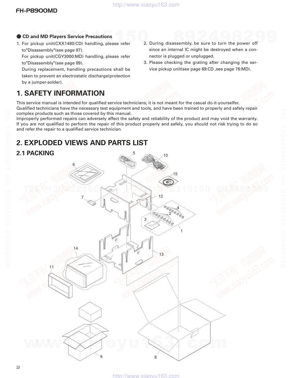
2. EXPLODED VIEWS AND PARTS LIST
2.1 PACKING
8
9
14
11
13
1
2
4
3
12
10
5
7
6
��
@@
��
��
��
@@
��
��
��
@@
��
��
��
@@
��
��
��
@@
��
��
��
@@
��
��
��
@@
��
��
��
@@
��
��
15
- CD and MD Players Service Precautions
1. For pickup unit(CXX1480:CD) handling, please refer
to"Disassembly"(see page 87).
For pickup unit(CGY3000:MD) handling, please refer
to"Disassembly"(see page 89).
During replacement, handling precautions shall be
taken to prevent an electrostatic discharge(protection
by a jumper-solder).
2. During disassembly, be sure to turn the power off
since an internal IC might be destroyed when a con-
nector is plugged or unplugged.
3. Please checking the grating after changing the ser-
vice pickup unit(see page 69:CD ,see page 76:MD).
1. SAFETY INFORMATION
This service manual is intended for qualified service technicians; it is not meant for the casual do-it-yourselfer.
Qualified technicians have the necessary test equipment and tools, and have been trained to properly and safely repair
complex products such as those covered by this manual.
Improperly performed repairs can adversely affect the safety and reliability of the product and may void the warranty.
If you are not qualified to perform the repair of this product properly and safely, you should not risk trying to do so
and refer the repair to a qualified service technician.
www. xiaoyu163. com
QQ 376315150
9
9
2
8
9
4
2
9
8
TEL 13942296513
9
9
2
8
9
4
2
9
8
0
5
1
5
1
3
6
7
3
Q
Q
TEL 13942296513 QQ 376315150 892498299
TEL 13942296513 QQ 376315150 892498299
http://www.xiaoyu163.com
3
FH-P8900MD
1 Screw Assy
CEA2719
2 Screw
BMZ50P060FMC
*
3 Polyethylene Bag
CEG-127
4 Screw
CMZ50P060FMC
5 Remote Control Assy
CXB3875
6-1 Polyethylene Bag
CEG1116
6-2 Owner’s Manual
CRB1651
6-3 Owner’s Manual
CRB1652
*
6-4 Caution Card
CRP1244
*
7 Battery
CEX1006
8 Carton
CHG4380
9 Contain Box
CHL4380
10 Cord Assy
CDE5893
11 Protector
CHP2273
12 Protector
CHP2227
13 Protector
CHP2272
14 Cover
CEG1074
15 Microphone Assy
CPM1054
Mark No. Description
Part No.
- PACKING SECTION PARTS LIST
NOTE:
- Parts marked by “*” are generally unavailable because they are not in our Master Spare Parts List.
- Screws adjacent to ∇ mark on the product are used for disassembly.
- Owner's Manual
Part No.
Language
CRB1651
English
CRB1652
Korean
www. xiaoyu163. com
QQ 376315150
9
9
2
8
9
4
2
9
8
TEL 13942296513
9
9
2
8
9
4
2
9
8
0
5
1
5
1
3
6
7
3
Q
Q
TEL 13942296513 QQ 376315150 892498299
TEL 13942296513 QQ 376315150 892498299
http://www.xiaoyu163.com
4
FH-P8900MD
2.2 EXTERIOR(1/2)
A
B
www. xiaoyu163. com
QQ 376315150
9
9
2
8
9
4
2
9
8
TEL 13942296513
9
9
2
8
9
4
2
9
8
0
5
1
5
1
3
6
7
3
Q
Q
TEL 13942296513 QQ 376315150 892498299
TEL 13942296513 QQ 376315150 892498299
http://www.xiaoyu163.com
5
FH-P8900MD
1 Screw
BMZ26P040FMC
2 Screw
BMZ26P060FMC
3 Screw
BMZ26P250FMC
4 Screw
BSZ30P060FMC
5 Screw
BSZ30P080FMC
6 Screw
BSZ30P160FMC
7 Screw
ISS26P055FUC
8 Screw(M2.6x14)
CBA1384
9 IC(IC334)
PAL005A
10 Transistor(Q909,912,915,921)2SD2396
11 IC(IC907)
PQ20RX1S-L
12 Fan Motor
CXM1169
13 IC(IC903)
BA033T
14 Bracket
CNC8729
15 Bracket
CNC9324
16 Cable
CDE6531
17 Cord
CDE6636
18 Cable
CDE6532
19 CD Mechanism Module(S9) CXK5510
20 •••••
21 Holder
CNC8971
*
22 Cushion
CNM6997
23 Heat Sink
CNR1580
24 •••••
25 Chassis Unit
CXB7050
26 Cap
CNV6727
27 MD Mechanism Module(MD-4LP)
CXK3320
28 Cord
CDE6261
29 Antenna Cable
CDH1284
30 Earth Plate
CNC9006
31 Cushion
CNM6870
32 Audio Amp Unit
CWM7640
33 Clamper
CEF1007
34 Terminal(CN453)
CKF1059
35 Plug(CN852)
CKM1278
36 Connector(CN171)
CKS2224
37 Connector(CN201)
CKS3124
38 Connector(CN802)
CKS3124
39 Connector(CN101)
CKS3408
40 Plug(CN801)
CKS3540
41 Connector(CN132)
CKS4060
42 Connector(CN851)
CKS4322
43 Connector(CN853)
CKS4322
44 Pin Jack(CN451)
CKX1046
45 Holder
CNC8724
46 Holder
CNC8725
47 Holder
CNC8727
48 Case
CNC8873
49 FM/AM Tuner Unit
CWE1563
50 Holder
CNC8815
51 Power Supply Unit
CWM7650
52 Screw
BMZ26P060FMC
53 Clamper
CEF1007
54 Plug(CN901)
CKS1242
55 Connector(CN904)
CKS2191
56 Connector(CN902)
CKS4321
57 Connector(CN903)
CKS4321
58 Heat Sink
CNR1579
59 Drive Unit
CXB7046
60 Screw
BMZ20P025FMC
61 Screw
BSZ30P060FMC
62 Screw(M2x3)
CBA1154
63 Screw(M2x2.5)
CBA1521
64 Washer
CBF1038
65 Spring
CBL1361
66 Spacer
CNM6202
67 Insulator
CNM6661
68 Spacer
CNM6923
69 Rack
CNV5299
70 Roller
CNV5301
71 Roller
CNV5814
72 Rack
CNV6149
73 Guide
CNV6291
74 Guide
CNV6399
75 Frame Unit
CXB5321
76 Chassis Unit
CXB7049
77 •••••
78 Motor Unit For Service
CXX1456
79 Gear Unit For Service
CXX1464
80 Screw
JFZ20P025FMC
81 Holder
CNV6741
82 Washer
CBF1039
83 Spring
CBL1493
84 Cord
CDE6282
85 Bracket
CNC8737
86 Gear
CNV5297
87 Gear
CNV5298
88 Gear
CNV6164
89 Gear
CNV6401
90 Bracket Unit
CXB5422
- EXTERIOR(1/2) SECTION PARTS LIST
Mark No. Description
Part No.
Mark No. Description
Part No.
www. xiaoyu163. com
QQ 376315150
9
9
2
8
9
4
2
9
8
TEL 13942296513
9
9
2
8
9
4
2
9
8
0
5
1
5
1
3
6
7
3
Q
Q
TEL 13942296513 QQ 376315150 892498299
TEL 13942296513 QQ 376315150 892498299
http://www.xiaoyu163.com
6
FH-P8900MD
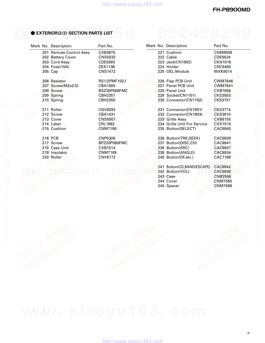
2.3 EXTERIOR(2/2)
D
C
243
www. xiaoyu163. com
QQ 376315150
9
9
2
8
9
4
2
9
8
TEL 13942296513
9
9
2
8
9
4
2
9
8
0
5
1
5
1
3
6
7
3
Q
Q
TEL 13942296513 QQ 376315150 892498299
TEL 13942296513 QQ 376315150 892498299
http://www.xiaoyu163.com
7
FH-P8900MD
201 Remote Control Assy
CXB3875
202 Battery Cover
CNS5032
203 Cord Assy
CDE5893
204 Fuse(10A)
CEK1136
205 Cap
CNS1472
206 Resistor
RS1/2PMF102J
207 Screw(M2x2.5)
CBA1085
208 Screw
BSZ30P060FMC
209 Spring
CBH2357
210 Spring
CBH2355
211 Roller
CNV6292
212 Screw
CBA1431
213 Cover
CNS5007
214 Label
CRL1962
215 Cushion
CNM7190
216 PCB
CNP5309
217 Screw
BPZ20P080FMC
218 Case Unit
CXB7014
219 Insulator
CNM7189
220 Roller
CNV6172
221 Cushion
CNM6938
222 Cable
CDE6534
223 Jack(CN1902)
CKN1016
224 Holder
CNC9462
225 OEL Module
MXK8014
226 Flap PCB Unit
CWM7646
227 Panel PCB Unit
CWM7641
228 Panel Unit
CXB7056
229 Socket(CN1101)
CKS3553
230 Connector(CN1102)
CKS3751
231 Connector(CN1901)
CKS3774
232 Connector(CN1903)
CKS3810
233 Grille Assy
CXB8155
234 Grille Unit For Service
CXX1510
235 Button(SELECT)
CAC6940
236 Button(TRK,SEEK)
CAC6939
237 Button(DISC,CH)
CAC6941
238 Button(SRC)
CAC6937
239 Button(ANGLE)
CAC6934
240 Button(DF,etc.)
CAC7188
241 Button(CD,BAND/ESCAPE)
CAC6942
242 Button(VOL)
CAC6938
243 Case
CNB2556
244 Cover
CNM7565
245 Spacer
CNM7569
- EXTERIOR(2/2) SECTION PARTS LIST
Mark No. Description
Part No.
Mark No. Description
Part No.
www. xiaoyu163. com
QQ 376315150
9
9
2
8
9
4
2
9
8
TEL 13942296513
9
9
2
8
9
4
2
9
8
0
5
1
5
1
3
6
7
3
Q
Q
TEL 13942296513 QQ 376315150 892498299
TEL 13942296513 QQ 376315150 892498299
http://www.xiaoyu163.com
8
FH-P8900MD
2.4 CD MECHANISM MODULE
E
www. xiaoyu163. com
QQ 376315150
9
9
2
8
9
4
2
9
8
TEL 13942296513
9
9
2
8
9
4
2
9
8
0
5
1
5
1
3
6
7
3
Q
Q
TEL 13942296513 QQ 376315150 892498299
TEL 13942296513 QQ 376315150 892498299
http://www.xiaoyu163.com
9
FH-P8900MD
Mark No. Description
Part No.
Mark No. Description
Part No.
1 Control Unit
CWX2499
2 Connector(CN701)
CKS1959
3 Connector(CN101)
CKS3486
4 Screw
BMZ20P025FMC
5 Screw
BSZ20P040FMC
6 Screw(M2x4)
CBA1362
7 Screw(M2x3)
CBA1527
8 Screw
CBA1545
9 Washer
CBF1037
10 Washer
CBF1038
11 Washer
CBF1039
12 Washer
CBF1060
13 Spring
CBH2378
14 Spring
CBH2379
15 Spring
CBH2380
16 Spring
CBH2381
17 Spring
CBH2382
18 Spring
CBH2383
19 Spring
CBH2384
20 Spring
CBH2385
21 Spring
CBH2386
22 Spring
CBH2387
23 Spring
CBH2390
24 Spring
CBH2391
25 Spring
CBH2392
26 Spring
CBH2426
27 Spring
CBH2444
28 Spring
CBL1494
29 Spring
CBL1495
30 Shaft
CLA3845
31 Roller
CLA3910
32 Frame
CNC8946
33 Lever
CNC8948
34 Lever
CNC8949
35 Arm
CNC8951
36 Arm
CNC9016
37 Arm
CNC9017
38 Bracket
CNC9123
39 Frame
CNC9263
40 Belt
CNT1086
41 Gear
CNV6886
42 Gear
CNV6316
43 Gear
CNV6317
44 Gear
CNV6318
45 Gear
CNV6319
46 Gear
CNV6320
47 Arm
CNV6322
48 Arm
CNV6323
49 Arm
CNV6324
50 Arm
CNV6325
51 Arm
CNV6326
52 Guide
CNV6327
53 Arm
CNV6924
54 Guide
CNV6329
55 Rack
CNV6330
56 Clamper
CNV6331
57 Arm
CNV6332
58 Guide
CNV6333
59 Cover
CNV6334
60 Arm
CNV6335
61 Guide
CNV6336
62 Roller
CNV6338
63 Damper
CNV6339
64 Damper
CNV6340
65 Guide
CNV6484
66 Chassis Unit
CXB5898
67 Arm Unit
CXB7983
68 Arm Unit
CXB5900
69 Arm Unit
CXB5901
70 Motor Unit(M2)
CXB5903
71 Screw Unit
CXB5904
72 Gear Unit
CXB5905
73 Bracket Unit
CXB6006
74 Motor Unit(M1)
CXB6007
75 Arm Unit
CXB6237
76 Screw(M2x5)
EBA1028
77 Screw
JFZ20P020FMC
78 Screw
JGZ17P020FZK
79 Washer
YE15FUC
80 Washer
YE20FUC
81 Pickup Unit(Service)(P9)
CXX1480
82 Screw
IMS26P030FMC
83 Guide
CNV6832
84 Connector(CN301)
CKS4282
85 Connector(CN302)
CKS2191
86 Spring
CBH2509
- CD MECHANISM MODULE SECTION PARTS LIST
www. xiaoyu163. com
QQ 376315150
9
9
2
8
9
4
2
9
8
TEL 13942296513
9
9
2
8
9
4
2
9
8
0
5
1
5
1
3
6
7
3
Q
Q
TEL 13942296513 QQ 376315150 892498299
TEL 13942296513 QQ 376315150 892498299
http://www.xiaoyu163.com
10
FH-P8900MD
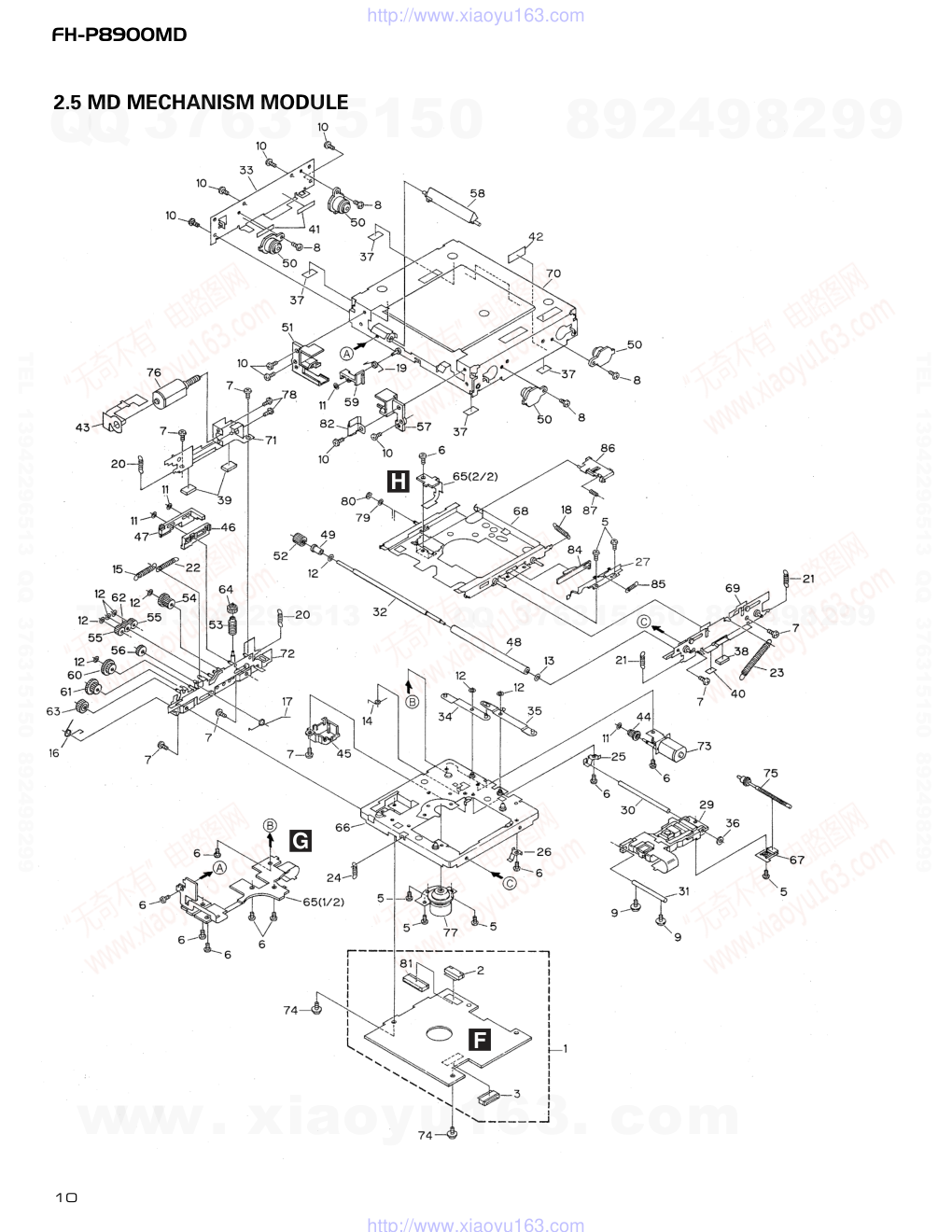
2.5 MD MECHANISM MODULE
F
G
H
www. xiaoyu163. com
QQ 376315150
9
9
2
8
9
4
2
9
8
TEL 13942296513
9
9
2
8
9
4
2
9
8
0
5
1
5
1
3
6
7
3
Q
Q
TEL 13942296513 QQ 376315150 892498299
TEL 13942296513 QQ 376315150 892498299
http://www.xiaoyu163.com
11
FH-P8900MD
1 MD Unit(MD-4LP)
CWX2505
2 Connector(CN401)
CKS4055
3 Connector(CN101)
CKS4056
4 •••••
5 Screw
CBA1537
6 Screw
CBA1538
7 Screw
CBA1539
8 Screw
CBA1540
9 Screw
CBA1541
10 Screw
CBA1542
11 Washer
CBF1037
12 Washer
CBF1038
13 Washer
CBF1039
14 Spring
CBH2213
15 Spring
CBH2440
16 Spring
CBH2243
17 Spring
CBH2441
18 Spring
CBH2217
19 Spring
CBH2218
20 Spring
CBH2437
21 Spring
CBH2438
22 Spring
CBH2214
23 Spring
CBH2442
24 Spring
CBH2289
25 Spring
CBL1405
26 Spring
CBL1406
27 Spring
CBL1519
28 •••••
29 PU Unit
CGY3000
30 Shaft
CLA3489
31 Shaft
CLA3490
32 Shaft
CLA3491
33 Bracket
CNC8418
34 Arm
CNC8269
35 Arm
CNC8270
36 Cushion
CNM6301
37 Sheet
CNM6323
38 Sheet
CNM6324
*
39 Sheet
CNM6653
40 Sheet
CNM7172
41 Sheet
CNM6727
42 Sheet
CNM6728
43 PCB
CNP5335
44 Gear
CNV5616
45 Holder
CNV5623
46 Rack
CNV5624
47 Rack
CNV5625
48 Roller
CNV5626
49 Collar
CNV5627
50 Damper
CNV5629
51 Guide
CNV5630
52 Gear
CNV5631
53 Gear
CNV5633
54 Gear
CNV5634
55 Gear
CNV5635
56 Gear
CNV5636
57 Guide
CNV5746
58 Lever
CNV5747
59 Lever
CNV5748
60 Gear
CNV5834
61 Gear
CNV5837
62 Gear
CNV5838
63 Gear
CNV5839
64 Gear
CNV5913
65 Composite PCB
CNX3127
66 Chassis Unit
CXB4399
67 Spring Unit
CXB4047
68 Holder Unit
CXB6415
69 Bracket Unit
CXB4049
70 Frame Unit
CXB4402
71 Bracket Unit
CXB4051
72 Bracket Unit
CXB6407
73 Motor Unit(-C)(M1)(CRG) CXB4054
74 Screw
IMS20P025FMC
75 Screw Unit(-C)
CXB4055
76 Motor Unit(-A)(M2)(Loading) CXB7603
77 Motor(M3)(SPDL)
CXM1181
78 Screw
JGZ14P018FZK
79 Washer
WB16FMC
80 Washer
YE12FUC
81 Connector(CN301)
CKS4060
82 Guide
CNC9597
83 •••••
84 Lever
CNV6670
85 Spring
CBH2477
86 Arm
CNV6541
87 Spring
CBH2443
Mark No. Description
Part No.
Mark No. Description
Part No.
- MD MECHANISM MODULE SECTION PARTS LIST
www. xiaoyu163. com
QQ 376315150
9
9
2
8
9
4
2
9
8
TEL 13942296513
9
9
2
8
9
4
2
9
8
0
5
1
5
1
3
6
7
3
Q
Q
TEL 13942296513 QQ 376315150 892498299
TEL 13942296513 QQ 376315150 892498299
http://www.xiaoyu163.com
12
FH-P8900MD
1
2
3
4
1
2
3
4
D
C
B
A
3. BLOCK DIAGRAM AND SCHEMATIC DIAGRAM
3.1 BLOCK DIAGRAM
FM/AM TUNER UNIT
A AUDIO AMP UNIT
CN451
LOCL
VDD
VCC
MAIN
ANTENNA
1
2
1
2
S1901
RESET SW
OEL+B
OEL+B
ILM+B
ILM+B
DPDT
KYDT
RESET
SW5V
KEY MATRIX
OEL+B
IC 1905
PD8082A
DISPLAY MIC
IC 1902
PD5640A
OEL CONTROLLER
IC 1906
PD3428A
OEL MODULE
CDVD
HOME
CD5VON
LRCK
CN171
CN1901
CN1903
VDD
MICSIG
MICSENS
1
2
4
1
8
32
31
X1901
14
16
IC 1901
RS-140
REM
ROM COMPUTER
VCC
C FLAP PCB UNIT
D
CN132
CN701
Q101
CONTROL UNIT
M
LASER
DIODE
MONITOR
DIODE
CLAMP
SENSE
DISC
SENSE
FOCUS ACT.
SPINDLE
MOTOR
M
CARRIAGE
MOTOR
LOAD/
TRACKING ACT.
LD-
MD
FO+
TO+
15
5
1
4
PU UNIT(SERVICE)(P9)
HOLOGRAM
UNIT
IC 401
BA5996FM
IC 201
TC9495F2
IC 701
BA05SFP
+5V REGULATOR
SERVO
CONTROL,
DSP,
LPF, DAC
CD
DRIVER
17
DSCSNS
DSCSNS
2
VD
VD
VDD
11
CONT
CONT
10
LOEJ
LOEJ
14
L-OUT
1
CD5VON
CN101
TOP
FOP
16
SOP
15
SOM
17
LCOP
18
LCOM
22
1
2
LOEJ
78
85
L_OUT
79
9
MUTE
12
FOP
TD/FD
AC,BD
F,E
SD/MD
38
RFI
43
FEI
4
14
TOP
S901
HOME
12EJ
SENSE
8EJ
SENSE
HOME
16
LD+
14
VDD
9
LDO
8
MDI
IC 101
TA2153FN
RFRPIN
FEO
TEO
24
16
14
46
TEI
RF-AMP
15
20
21
11
12
1 13
IC 1903
S-80734ANDYI
RESET
2
VDD
OEL+B
OEL+B
CN1902
VDD
Q401
ST
SD
6
5
1
1
CN201
CN302
MCK
MCK
XIN 78
BSIO
BSCK
BSRQ
PVD
MDVD
RESET
M
M
M
LASER
DIODE
MONITOR
DIODE
FOCUS ACT.
LOADING
MOTOR
DISC SW
LOAD SW
HOME SW
CLMP SW
SPDL
MOTOR
EJCT
SW
CRG
MOTOR
TRACKING ACT.
LD+
MON
F+
T+
LO—
LO+
SO—
SO+
EJECT
DISC
LOAD
HOME
CLMP
14
19
1,2
3
10
12
11
9
10
14
13
15
17
3
2
34
33
XOUT
AUX2
AUX1
XIN
ESW
DISC
LSW
HOME
CSW
7
25
15
1
5
3
93
20
AOOTL
28
XRST
FEA
AUX
96
VREF
86
VDDSW
75
MUTE
95
VDSENSE
44
VDON
34
BSI
33
BSO
37
bsrq
17
brst
35
BSCK
38
BRXEN
10
reset
MDVD
VDCONT
MDVD
BDAT
BRQ
BRST
BCK
BRX
BRXEN
MRST
21
84
10
11
9
7
6
5
4
3
1
13
10
9
7
6
5
4
3
1
13
14
19
1,2
3
G SW1 PCB
F MD UNIT
H
SW2 PCB
PU UNIT
CN101
IC 101
CXA2523AR
IC 401
BA5985FM
IC 201
CXD2667R
CN401
Q101
Q102
UMD2N
IC 102
NJM2115V
IC 304
TC7WH34FU
IC 301
PD5655A
IC 302, 303
TC7WT125FU
X201
11
81
82
79
83
80
13
LDCNT
43
X301
Q301
Q602
Q601
VDD
3VD
PVD
1
3
IC 701
BA033FP
5
11
4
3
7
9
6
8
10
17
11
18
19
PVD
PVD
2
1
20
21
MDL
16
6
1
15
13
16
14
12
CN301
HOLOGRAM
UNIT
RF AMP
DIGITAL
SERVO
RTRAC
5ch Pow-Driver
MD SYSTEM CONTROLLER
D RAM
3V Regulator
B
E
IC 3
EEPROM
28
27
FM/AM 1ST IF 10.7MHz
T51 Q51 CF51
CF52 CF53
IC1
MIXER, IF AMP, DET.
6
18
LDET
22
25
10
14
12
15 16
13
2
CF202
VDD
VCC
DI/DO
CE2
CK
CE1
SL
FMSD
IC 2 FM MPX
AMANT
FMANT
ATT
ATT
AMRF
FMRF
IMG ADJ
RF ADJ
X901
10.25MHz
ANT ADJ
LOCL
23
LOCH
AMDET
MPXREF 41kHz
AM 2ND IF
450kHz
19
CREQ
1
STIND
L ch
20
17
7
NC
NC
WC
26 RFGND
LOCH
PCE2
PDIO
PCE1
PCK
SL
www. xiaoyu163. com
QQ 376315150
9
9
2
8
9
4
2
9
8
TEL 13942296513
9
9
2
8
9
4
2
9
8
0
5
1
5
1
3
6
7
3
Q
Q
TEL 13942296513 QQ 376315150 892498299
TEL 13942296513 QQ 376315150 892498299
http://www.xiaoyu163.com
13
FH-P8900MD
5
6
7
8
5
6
7
8
D
C
B
A
BUP
BUP
10
4
9
FLPOPN
CDVD
BUP
44
FLPCLS
45
FLAPPW
43
1
bsens
73
asens
74
VDSENS
92
SPFL
SPRL
SYSPW
12
14
22
4
25
44
2
8
1
RL—
23
RL+
21
FL—
3
FL+
RL—
ACC
GND
BUP
BUP
BUP
RL+
FL—
BREM
FL+
FL
SUBL
5
AM
16
4
1
3
36
MD L
3
LOCL
3
PDIO
1
4
LOCH
80
PCE2
81
ST
90
SD
SL
91
PCE1
89
PCK
2
MPX-RDS
16
IC 251(1/2)
PML011A
IC 334
PAL005A
ELECTRONIC VOLUME/
SOURCE SELECTOR
DSP
MIX
POWER AMP
E VOL
SYSTEM
MICRO COMPUTER
IC 601 (1/2)
PD5694A
MUTE
STBY
B.REM
Q820
Q851
Q852
2
1
5
9
11
10
12
4
ILL
3
ANT1
6
TELMUTE
8
CN852
A
IC 804
BA6288FS
11
6
14
3
5
4
MT2
MT1
1
2
CN802
MOTOR
UNIT
X2
10
X1
11
X601
6.291456MHz
SWVDD
39
FLSEN1
82
FLSEN0
81
IC 801
TC7W14FU
7
5
1
3
IC 802
GP1S94J
1
2
IC 803
GP1S94J
1
2
SW5V
VDD
IC 205
NJM4558MD
LRCK
58 BFOT
76 LRCK
DSP
IC 201
PDG262A
IC 332
NJM4558MD
5
7
IC 333
NJM4558MD
3
1
5
7
35
25
37
27
39
29
AOUTL2
39
AOUTL3
52
AOUTL1
27
IC 251(2/2)
PML011A
IC 202
TC74VHC126FT
IC 203
TC7S08FU
MCK_OUT
57
DSPMS
61
DPDT
36
KEYDT
37
MICSENS
38
RESET
12
flapejsw
85
fopnsw
83
fclssw
84
S801 FEJSW
S802 FOPNSW
S803 FCLSSW
Q855
Q853
Q331
XTALI38
42
XTALO38
41
X251
16.9344MHz
BUP
Q856
A
Q332
Q937
1
1
CN853
1
5
6
2
CN901
CN903
CN903
CN853
Q938
Q927
Q935
Q936
BUP
Q916
Q917
Q915
BUP
Q932
Q931
Q854
Q913
Q914
Q912
Q933
BZ901
ALARM
BUZZER
BUP
Q926
Q925
3
2
IC 902
S-81250SGUP
3
2
1
IC 907
PQ20RX1S-L
3
1
IC 903
BA033T
IC 904
HA12187FP
1
2
6
5
5
BUP
Q922
Q923
Q921
8
1
5
CN101
CDVD
A8V
TUNVDD
LED+8
A3V
MDVD
BUS—
BUS+
ASENB
ILL
VDD
VDD
Q929
Q928
Q930
SYSPW
HOME
LOEJ
CONT
27
48
49
CD5VON
77
DSCSNS
94
Q802
Q804
Q805
FLAPILM
35
BUP
1
3
4
5
9
10
14
20
2
19
18
17
16
8
7
10
9
11
12
6
17
5
11
OEL+B
IC 602
S-80734ANDYI
2
1
ILM+B
OEL+B
OEL+B
OEL+B
OEL+B
ILM+B
ILM+B
DPDT
KYDT
RESET
SW5V
ILM+B
FLPILM+B
DPDT
KYDT
RESET
SWVDD
VDD
VDD
L+B
MUTE
FL
SWL
MUTE
TELIN
ISENS
ASENBO
VDCNTCD
MUTE
SYSPW
PEE
OELPW
VDSEL
VDCNTMD
ANTPW
TX
RX
IPPW
DALMON
26
TEL_IN
25
isens
20
ASENBO
87
VDCONT
56
SYSPW
19
PEE
24
OELPW
22
VDSEL
67
AUTOANT
23
IPBUSOUT
30
IPBUSIN
29
IPPW
10
DALMON
18
16
15
27
23
30
29
6
16
15
27
23
30
29
6
28
28
CN902
CN851
30
30
28
28
13
13
10
10
17
17
14
14
11
11
15
15
16
16
29
29
CN903
CN853
9
9
24
24
CN851
CN902
18
18
CN853
CN903
2
2
3
3
7
7
11
11
4
4
31
31
8
8
25
25
10
10
5
5
SYSTEM
MICRO COMPUTER
IC 601 (2/2)
PD5694A
RESET
CN1101
CN801
CN1901
CN1102
VDD
10
12
13
13
24
25
27
2
1
3
4
14
15
16
MICSIG
MICSENS
21
12
22
13
19
D PANEL PCB UNIT
B POWER SUPPLY
UNIT
TELMUTE
ILL
ASEN(IP)
CD+B
SYS+B
TU5V
LED+B
DSP+B
PVD
MDVD
ANT+B
BUS+
BUS—
FANB
FANG
RESET
Q941
Q909
Q910
Q911
4
2
1
IC 901
BA08SFP
PVD
BUP
1
6
IC 906
TPD1018F
B
MOTOR CONTROLLER
SLIDE POSITION SENSE
RCA
CD
REG.
SYS
REG.
TUNVDD REG.
LED REG.
DSP REG.
IP-DRIVER
FAN REG.
IP-BUS
brxen
brst
BSO,BSI
BSCK
69
70
31,32
34
bsrq
71
1
2
CN904
FAN
CN1902
BSIO
Q803
Q301
C
C
Q301
IC 805
BA09SFP
4
2
www. xiaoyu163. com
QQ 376315150
9
9
2
8
9
4
2
9
8
TEL 13942296513
9
9
2
8
9
4
2
9
8
0
5
1
5
1
3
6
7
3
Q
Q
TEL 13942296513 QQ 376315150 892498299
TEL 13942296513 QQ 376315150 892498299
http://www.xiaoyu163.com
14
FH-P8900MD
1
2
3
4
1
2
3
4
D
C
B
A
3.2 OVERALL CONNECTION DIAGRAM(GUIDE PAGE)
Note: When ordering service parts, be sure to refer to “EXPLODED VIEWS AND PARTS LIST” or “ELECTRICAL PARTS
LIST”.
A-a
A-b
A-a
A-a
A-b
A-b
A-b
A-b
A-a
A-a
Large size
SCH diagram
Guide page
Detailed page
A
A-a
MIC.
RESET
MIC. SENSE
PD5694A
SYSTEN CONT
CN802
E
CN701
CN302
F
CN301
FM/AM TUNER UNIT
MOTOR
UNIT
D
S801:
S802:
S803:
FEJSW
FOPNSW
FCLSSW
H
H
L
L
H
H
L
L
H
Full close
CD eject
Full open
MD UNIT
CONTROL UNIT
PANEL PCB
6.1V
5.00V
4.91V
7.57V
5.2V(PLAY)
3.28V
5.25V
3.51V
3.51V
5.11V
14.20V
9.09V
8.38V
5.23V
4.53V
8.81V
8.85V
FM:-12.3dBs
AM:-25.1dBs
IP-BUS: -6.0dBs
MD: -6.7dBs
FM(100%):-19.3dBs
AM(30%):-31.1dBs
IP-BUS:+2.0dBs
MD:+1.3dBs
www. xiaoyu163. com
QQ 376315150
9
9
2
8
9
4
2
9
8
TEL 13942296513
9
9
2
8
9
4
2
9
8
0
5
1
5
1
3
6
7
3
Q
Q
TEL 13942296513 QQ 376315150 892498299
TEL 13942296513 QQ 376315150 892498299
http://www.xiaoyu163.com
15
FH-P8900MD
5
6
7
8
5
6
7
8
D
C
B
A
A
A-b
CENTER POINT:1.65V
TROLLER
SOURCE
R708
L239
: The power supply is shown with the marked box.
>
>
A AUDIO AMP UNIT
CN1101
B
CN903
B
CN902
Decimal points for resistor
and capacitor fixed values
are expressed as :
2.2 2R2
0.022 R022
←
←
The > mark found on some component parts indicates
the importance of the safety factor of the part.
Therefore, when replacing, be sure to use parts of
identical designation.
Symbol indicates a resistor.
No differentiation is made between chip resistors and
discrete resistors.
NOTE :
Symbol indicates a capacitor.
No differentiation is made between chip capacitors and
discrete capacitors.
B UNIT
> 10A
8.84V
3.19V
3.28V
1.53V
1.44V
4.25V
14.23V
14.23V
14.23V
14.31V
12.06V
14.21V
5.03V
8.20V
8.81V
5.39V
6.08V
8.83V
5.03V
9.04V
14.10V
14.02V
FM:+28.9dBs
AM:+16.1dBs
IP-BUS:+35.2dBs
CD:+35.8dBs
MD:+34.5dBs
FM: -4.1dBs
AM:-16.9dBs
IP-BUS: +2.2dBs
CD: +2.8dBs
MD: +1.5dBs
FM:-10.9dBs
AM:-23.7dBs
IP-BUS: -4.6dBs
MD: -5.3dBs
FM: -8.5dBs
AM:-21.3dBs
IP-BUS: -2.2dBs
CD: -1.7dBs
MD: -2.9dBs
FM: +2.9dBs
AM: -9.9dBs
IP-BUS: +9.2dBs
CD: +9.8dBs
MD: +8.5dBs
www. xiaoyu163. com
QQ 376315150
9
9
2
8
9
4
2
9
8
TEL 13942296513
9
9
2
8
9
4
2
9
8
0
5
1
5
1
3
6
7
3
Q
Q
TEL 13942296513 QQ 376315150 892498299
TEL 13942296513 QQ 376315150 892498299
http://www.xiaoyu163.com
16
FH-P8900MD
1
2
3
4
1
2
3
4
D
C
B
A
CENT
E
CN701
CN302
F
CN301 MD UNIT
CONTROL UNIT
6.1V
5.00V
4.91V
7.57V
5.2V(PLAY)
3.28V
5.25V
3.51V
3.51V
FM:-12.3dBs
AM:-25.1dBs
IP-BUS: -6.0dBs
MD: -6.7dBs
IP-BUS:+2.0dBs
MD:+1.3dBs
A-a A-b
A-a
1
2
3
www. xiaoyu163. com
QQ 376315150
9
9
2
8
9
4
2
9
8
TEL 13942296513
9
9
2
8
9
4
2
9
8
0
5
1
5
1
3
6
7
3
Q
Q
TEL 13942296513 QQ 376315150 892498299
TEL 13942296513 QQ 376315150 892498299
http://www.xiaoyu163.com
17
FH-P8900MD
5
6
7
8
5
6
7
8
D
C
B
A
CENT
MIC.
RESET
MIC. SENSE
PD5694A
SYSTEN CONTROLLER
CN802
FM/AM TUNER UNIT
MOTOR
UNIT
D
S801:
S802:
S803:
FEJSW
FOPNSW
FCLSSW
H
H
L
L
H
H
L
L
H
Full close
CD eject
Full open
PANEL PCB UNIT
5 03V
14
14.02V
5.11V
14.20V
9.09V
8.38V
5.23V
4.53V
8.81V
8.85V
FM(100%):-19.3dBs
AM(30%):-31.1dBs
A-a A-b
A-a
4
5
6
www. xiaoyu163. com
QQ 376315150
9
9
2
8
9
4
2
9
8
TEL 13942296513
9
9
2
8
9
4
2
9
8
0
5
1
5
1
3
6
7
3
Q
Q
TEL 13942296513 QQ 376315150 892498299
TEL 13942296513 QQ 376315150 892498299
http://www.xiaoyu163.com
18
FH-P8900MD
1
2
3
4
1
2
3
4
D
C
B
A
CENTER POINT:1.65V
R708
A AUDIO AMP UNIT
8.84V
3.19V
3.28V
1.53V
1.44V
4.25V
14.23V
FM:+28.9dBs
AM:+16.1dBs
IP-BUS:+35.2dBs
CD:+35.8dBs
MD:+34.5dBs
FM: -4.1dBs
AM:-16.9dBs
IP-BUS: +2.2dBs
CD: +2.8dBs
MD: +1.5dBs
FM:-10.9dBs
AM:-23.7dBs
IP-BUS: -4.6dBs
MD: -5.3dBs
FM: -8.5dBs
AM:-21.3dBs
IP-BUS: -2.2dBs
CD: -1.7dBs
MD: -2.9dBs
FM: +2.9dBs
AM: -9.9dBs
IP-BUS: +9.2dBs
CD: +9.8dBs
MD: +8.5dBs
A-a A-b
A-b
1
2
3
www. xiaoyu163. com
QQ 376315150
9
9
2
8
9
4
2
9
8
TEL 13942296513
9
9
2
8
9
4
2
9
8
0
5
1
5
1
3
6
7
3
Q
Q
TEL 13942296513 QQ 376315150 892498299
TEL 13942296513 QQ 376315150 892498299
http://www.xiaoyu163.com
19
FH-P8900MD
5
6
7
8
5
6
7
8
D
C
B
A
CENTER POINT:1.65V
ROLLER
SOURCE
R708
L239
: The power supply is shown with the marked box.
>
>
CN1101
B
CN903
B
CN902
Decimal points for resistor
and capacitor fixed values
are expressed as :
2.2 2R2
0.022 R022
←
←
The > mark found on some component parts indicates
the importance of the safety factor of the part.
Therefore, when replacing, be sure to use parts of
identical designation.
Symbol indicates a resistor.
No differentiation is made between chip resistors and
discrete resistors.
NOTE :
Symbol indicates a capacitor.
No differentiation is made between chip capacitors and
discrete capacitors.
B UNIT
> 10A
14.23V
14.23V
14.23V
14.31V
12.06V
14.21V
5.03V
8.20V
8.81V
5.39V
6.08V
8.83V
5.03V
9.04V
14.10V
14.02V
IP-BUS: +9.2dBs
CD: +9.8dBs
MD: +8.5dBs
A-a A-b
A-b
4
5
6
www. xiaoyu163. com
QQ 376315150
9
9
2
8
9
4
2
9
8
TEL 13942296513
9
9
2
8
9
4
2
9
8
0
5
1
5
1
3
6
7
3
Q
Q
TEL 13942296513 QQ 376315150 892498299
TEL 13942296513 QQ 376315150 892498299
http://www.xiaoyu163.com
FH-P8900MD
20
R970
R971
R972
R973
R970-973:
12
HA12187FP
A CN853
A CN851
A
1
2
3
4
B
C
D
1
2
3
4
3.3 POWER SUPPLY UNIT
B
www. xiaoyu163. com
QQ 376315150
9
9
2
8
9
4
2
9
8
TEL 13942296513
9
9
2
8
9
4
2
9
8
0
5
1
5
1
3
6
7
3
Q
Q
TEL 13942296513 QQ 376315150 892498299
TEL 13942296513 QQ 376315150 892498299
http://www.xiaoyu163.com
21
FH-P8900MD
RCA CORD
B POWER SUPPLY UNIT
FAN
5
6
7
8
A
B
C
D
5
6
7
8B
www. xiaoyu163. com
QQ 376315150
9
9
2
8
9
4
2
9
8
TEL 13942296513
9
9
2
8
9
4
2
9
8
0
5
1
5
1
3
6
7
3
Q
Q
TEL 13942296513 QQ 376315150 892498299
TEL 13942296513 QQ 376315150 892498299
http://www.xiaoyu163.com
22
FH-P8900MD
OE
D
CN1102
DF
CONNECT WITH OEL HOLDER
VOLTAGE 14.4V : 16mA - 17mA
RESET
A
1
2
3
4
B
C
D
1
2
3
4
3.4 FLAP PCB UNIT
C
www. xiaoyu163. com
QQ 376315150
9
9
2
8
9
4
2
9
8
TEL 13942296513
9
9
2
8
9
4
2
9
8
0
5
1
5
1
3
6
7
3
Q
Q
TEL 13942296513 QQ 376315150 892498299
TEL 13942296513 QQ 376315150 892498299
http://www.xiaoyu163.com
23
FH-P8900MD
OEL MODULE
C
FLAP PCB UNIT
DISPLAY and
KEY MICROCOMPUTER
OEL CONTROLLER
ROM
5
6
7
8
A
B
C
D
5
6
7
8C
www. xiaoyu163. com
QQ 376315150
9
9
2
8
9
4
2
9
8
TEL 13942296513
9
9
2
8
9
4
2
9
8
0
5
1
5
1
3
6
7
3
Q
Q
TEL 13942296513 QQ 376315150 892498299
TEL 13942296513 QQ 376315150 892498299
http://www.xiaoyu163.com
24
FH-P8900MD
D
A
PANEL PCB UNIT
CN801
C
CN1901
A
1
2
3
4
B
C
D
1
2
3
4
3.5 PANEL PCB UNIT
D
www. xiaoyu163. com
QQ 376315150
9
9
2
8
9
4
2
9
8
TEL 13942296513
9
9
2
8
9
4
2
9
8
0
5
1
5
1
3
6
7
3
Q
Q
TEL 13942296513 QQ 376315150 892498299
TEL 13942296513 QQ 376315150 892498299
http://www.xiaoyu163.com
25
FH-P8900MD
www. xiaoyu163. com
QQ 376315150
9
9
2
8
9
4
2
9
8
TEL 13942296513
9
9
2
8
9
4
2
9
8
0
5
1
5
1
3
6
7
3
Q
Q
TEL 13942296513 QQ 376315150 892498299
TEL 13942296513 QQ 376315150 892498299
http://www.xiaoyu163.com
FH-P8900MD
1
2
3
4
1
2
3
4
D
C
B
A
26
3.6 CD MECHANISM MODULE
E
M1 CXB6007
M2 CXB5903
LOADING/CARRIAGE
SPINDLE
RF AMP
S
ACT/MOTOR DRIVER
5V REGULATOR
CN101
E
CONTROL UNIT
PICKUP UNIT(SERVICE)(P9)
www. xiaoyu163. com
QQ 376315150
9
9
2
8
9
4
2
9
8
TEL 13942296513
9
9
2
8
9
4
2
9
8
0
5
1
5
1
3
6
7
3
Q
Q
TEL 13942296513 QQ 376315150 892498299
TEL 13942296513 QQ 376315150 892498299
http://www.xiaoyu163.com
FH-P8900MD
5
6
7
8
5
6
7
8
D
C
B
A
27
E
SERVO CONTROL/DSP/DAC/LPF
ER
CN701
CN301
CN302
SWITCHES:
CONTROL UNIT
S901 : HOME SWITCH.....ON-OFF
S902 : CLAMP SWITCH....ON-OFF
S903 : DSCSNS SWITCH....ON-OFF
S904 : 12EJ SWITCH....ON-OFF
S905 : 8EJ SWITCH....ON-OFF
The underlined indicates the switch position.
A
CN171
A
CN201
www. xiaoyu163. com
QQ 376315150
9
9
2
8
9
4
2
9
8
TEL 13942296513
9
9
2
8
9
4
2
9
8
0
5
1
5
1
3
6
7
3
Q
Q
TEL 13942296513 QQ 376315150 892498299
TEL 13942296513 QQ 376315150 892498299
http://www.xiaoyu163.com
28
FH-P8900MD
@ CH1:BCK
2V/div.
During "Play"
1 CH1:DSCSNS
5V/div.
2 CH2:CLCONT
5V/div.
3 CH3:LOEJ
5V/div.
4 CH4:VD
10V/div.
When loading (8 cm CD)
500ms/div.
5 CH1:FD
500mV/div.
6 CH2:FOK
5V/div.
7 CH3:MD
5V/div.
When setting up "Source On"
500ms/div.
8 CH1:FE
500mV/div.
9 CH2:FOON 5V/div.
When setting up "Source On"
500ms/div.
5 CH1:FD
500mV/div.
6 CH2:FOK
5V/div.
7 CH3:MD
5V/div.
Magnified drawing for "time"
100ms/div.
1 CH1:DSCSNS
5V/div.
2 CH2:CLCONT
5V/div.
3 CH3:LOEJ
5V/div.
4 CH4:VD
10V/div.
When loading (12 cm CD)
Ref. :
GND
Mode :
Normal
Ref. :
GND
Mode :
Normal
Ref. :
VREF
Mode :
Normal
Ref. :
VREF
Mode :
Normal
Ref. :
VREF
Mode :
Normal
Ref. :
VREF
Mode :
Normal
Ref. :
VREF
Mode :
Normal
Ref. :
VREF
Mode :
Normal
Ref. :
VREF
Mode :
Normal
Ref. :
VREF
Mode :
Test
Ref. :
VREF
Mode :
Normal
Ref. :
VREF
Mode :
Normal
500ms/div.
0 CH1:TE
500mV/div.
8 CH2:FE
500mV/div.
When setting up "Source On"
200ms/div.
1µs/div.
# CH1:LRCK
2V/div.
$ CH2:DOUT 2V/div.
During "Play"
10µs/div.
7 CH1:MD
500mV/div.
During "Play"
10µs/div.
% CH1:RFO
500mV/div.
During "Play"
0.5µs/div.
% CH1:RFO
500mV/div.
0 CH2:TE
500mV/div.
During "Tracking Open"
2ms/div.
8 CH1:FE
500mV/div.
5 CH2:FD
500mV/div.
0 CH3:TE
500mV/div.
! CH4:TD
500mV/div.
During "Play"
1ms/div.
- Waveforms
Note:1. The encircled numbers denote measuring pointes in the circuit diagram.
2. Reference voltage
VREF:2.1V
www. xiaoyu163. com
QQ 376315150
9
9
2
8
9
4
2
9
8
TEL 13942296513
9
9
2
8
9
4
2
9
8
0
5
1
5
1
3
6
7
3
Q
Q
TEL 13942296513 QQ 376315150 892498299
TEL 13942296513 QQ 376315150 892498299
http://www.xiaoyu163.com
29
FH-P8900MD
% CH1:RFO
1V/div.
0 CH2:TE
500mV/div.
& CH3:DFCT
5V/div.
During inside/outside search
200ms/div.
% CH1:RFO
1V/div.
0 CH2:TE
500mV/div.
! CH3:TD
1V/div.
1 Track Jump
500µs/div.
% CH1:RFO
1V/div.
0 CH2:TE
1V/div.
! CH3:TD
1V/div.
100 Track Jump
5ms/div.
% CH1:RFO
1V/div.
0 CH2:TE
1V/div.
! CH3:TD
1V/div.
32 Track Jump
5ms/div.
5 CH1:FD
1V/div.
^ CH2:FOP
2V/div.
With no disk inserted
During "Focus Close"
200ms/div.
1 CH1:DSCSNS
5V/div.
2 CH2:CLCONT
5V/div.
3 CH3:LOEJ
5V/div.
When "Eject" (8cm CD)
200ms/div.
* CH1:TEY
500mV/div.
( CH2:SD
2V/div.
During inside/outside search
200ms/div.
1 CH1:DSCSNS
5V/div.
2 CH2:CLCONT
5V/div.
3 CH3:LOEJ
5V/div.
When "Eject" (12 cm CD)
200ms/div.
% CH1:RFO
2V/div.
& CH2:DFCT
5V/div.
5 CH3:FD
1V/div.
! CH4:TD
2V/div.
When reproducing black dots (800µm)
500µs/div.
Ref. :
VREF
Mode :
Test
Ref. :
VREF
Mode :
Test
Ref. :
VREF
Mode :
Normal
Ref. :
VREF
Mode :
Normal
Ref. :
VREF
Mode :
Test
Ref. :
VREF
Mode :
Test
Ref. :
VREF
Mode :
Normal
Ref. :
GND
Mode :
Normal
Ref. :
GND
Mode :
Normal
) CH1:TX
2V/div.
"Play" in 1kHz, 0dB
1µs/div.
Ref. :
GND
Mode :
Normal
(REC)
www. xiaoyu163. com
QQ 376315150
9
9
2
8
9
4
2
9
8
TEL 13942296513
9
9
2
8
9
4
2
9
8
0
5
1
5
1
3
6
7
3
Q
Q
TEL 13942296513 QQ 376315150 892498299
TEL 13942296513 QQ 376315150 892498299
http://www.xiaoyu163.com
30
FH-P8900MD
1
2
3
4
1
2
3
4
D
C
B
A
3.7 MD MECHANISM MODULE (GUIDE PAGE)
F
M1
CXB4054
D
FOCUS SERVO LINE
TRACKING SERVO LINE
CARRIAGE SERVO LINE
SPINDLE SERVO LINE
F
T
C
S
S
S
C
C
T
T
F
F
C
C
S
S
T
T
F
F
S
S
C
C
C
C
S
S
F
T
T
F
1
(
0
4
6
5
@
!
)
fi
‹
fl
¤
›
⁄
·
*
RF AMP
&
5ch Pow-Driver
F-a
G
www. xiaoyu163. com
QQ 376315150
9
9
2
8
9
4
2
9
8
TEL 13942296513
9
9
2
8
9
4
2
9
8
0
5
1
5
1
3
6
7
3
Q
Q
TEL 13942296513 QQ 376315150 892498299
TEL 13942296513 QQ 376315150 892498299
http://www.xiaoyu163.com
31
FH-P8900MD
5
6
7
8
5
6
7
8
D
C
B
A
CK SELECT
22.5792MHz
CSS1512
A CN991
MD UNIT
C
MD SYSTEM
CONTROLLER
3-5V
LEVEL SHIFT
F
F
T
T
2
3
7
$
8
9
°
%
^
‡
3.3V Reg
DIGITAL SERVO
ATRAC,ATRAC3 DECODER
#
F
CN132
F-b
MD UNIT
F
www. xiaoyu163. com
QQ 376315150
9
9
2
8
9
4
2
9
8
TEL 13942296513
9
9
2
8
9
4
2
9
8
0
5
1
5
1
3
6
7
3
Q
Q
TEL 13942296513 QQ 376315150 892498299
TEL 13942296513 QQ 376315150 892498299
http://www.xiaoyu163.com
32
FH-P8900MD
A
1
2
3
4
B
C
D
1
2
3
4
FOCUS SERVO LINE
TRACKING SERVO LINE
CARRIAGE SERVO LINE
SPINDLE SERVO LINE
F
T
C
S
S
S
C
C
F
T
T
F
1
·
*
RF AMP
&
1
2
3
4
5
F-a
F-a
F-b
www. xiaoyu163. com
QQ 376315150
9
9
2
8
9
4
2
9
8
TEL 13942296513
9
9
2
8
9
4
2
9
8
0
5
1
5
1
3
6
7
3
Q
Q
TEL 13942296513 QQ 376315150 892498299
TEL 13942296513 QQ 376315150 892498299
http://www.xiaoyu163.com
33
FH-P8900MD
5
6
7
8
A
B
C
D
5
6
7
8
M1
CXB4054
D
T
T
F
F
C
C
S
S
T
T
F
F
S
S
C
C
C
C
S
S
(
0
4
6
5
@
!
)
fi
‹
fl
¤
›
⁄
5ch Pow-Driver
6
7
8
9
10
F-a
G
F-a
F-b
www. xiaoyu163. com
QQ 376315150
9
9
2
8
9
4
2
9
8
TEL 13942296513
9
9
2
8
9
4
2
9
8
0
5
1
5
1
3
6
7
3
Q
Q
TEL 13942296513 QQ 376315150 892498299
TEL 13942296513 QQ 376315150 892498299
http://www.xiaoyu163.com
34
FH-P8900MD
A
1
2
3
4
B
C
D
1
2
3
4
22.5792MHz
CSS1512
MD UNIT
C
F
F
T
T
2
3
7
$
8
9
°
%
^
‡
3.3V Reg
DIGITAL SERVO
ATRAC,ATRAC3 DECODER
#
1
2
3
4
5
MD UNIT
F-b
F-a
F-b
F
www. xiaoyu163. com
QQ 376315150
9
9
2
8
9
4
2
9
8
TEL 13942296513
9
9
2
8
9
4
2
9
8
0
5
1
5
1
3
6
7
3
Q
Q
TEL 13942296513 QQ 376315150 892498299
TEL 13942296513 QQ 376315150 892498299
http://www.xiaoyu163.com
35
FH-P8900MD
CK SELECT
A CN991
MD SYSTEM
CONTROLLER
3-5V
LEVEL SHIFT
5
6
7
8
A
B
C
D
5
6
7
8
CN132
F-b
6
7
8
9
10
F-a
F-b
www. xiaoyu163. com
QQ 376315150
9
9
2
8
9
4
2
9
8
TEL 13942296513
9
9
2
8
9
4
2
9
8
0
5
1
5
1
3
6
7
3
Q
Q
TEL 13942296513 QQ 376315150 892498299
TEL 13942296513 QQ 376315150 892498299
http://www.xiaoyu163.com
36
FH-P8900MD
1 RF
0.5V/div. 0.5µs/div.
Normal mode: Play
1 CH1: RF
0.5V/div.
2 CH2: MNT3
2V/div.
(OFTRK)
Test mode: Tracking open
0.5ms/div.
1 CH1: RF
0.5V/div.
3 CH2: MNT2
2V/div.
(DFCT)
Test mode: The defect part passes 800µm
0.5ms/div.
4 CH1: FIN
0.2V/div.
5 CH2: FOP
1V/div.
6 CH2: FOM
1V/div.
Test mode: No disc, Focus close
0.5s/div.
4 CH1: FIN
0.1V/div.
7 CH2: MNT0
2V/div.
(FOK)
Normal mode: Focus close
0.1s/div.
8 CH1: FEY
0.2V/div.
9 CH2: TEY
1V/div.
Normal mode: Focus close
2ms/div.
9 CH1: TEY
1V/div.
0 CH2: TIN
0.2V/div.
Test mode: 32 tracks jump (REV)
0.5ms/div.
9 CH1: TEY
1V/div.
0 CH2: TIN
0.2V/div.
Test mode: Single jump (REV)
0.5ms/div.
9 CH1: TEY
1V/div.
0 CH2: TIN
0.2V/div.
! CH3: CIN
0.5V/div.
Test mode: Fine jump (REV)
5ms/div.
8 CH1: FEY
0.2V/div.
4 CH2: FIN
0.2V/div.
Normal mode: Play
20ms/div.
4 CH1: FIN
0.1V/div.
@ CH2: SIN
0.5V/div.
Normal mode: Play
0.5s/div.
4 CH1: FIN
0.1V/div.
@ CH2: SIN
0.5V/div.
Normal mode: Play(Recordable MD)
0.5s/div.
- Waveforms
Note:1. Circled figures represent the measuring points in the circuit diagram.
2. Reference voltage VC:1.65V<·VC>
3. Premastered MD,Make measurements using the MMD110.
Nonetheless,waveforms indicated as"Recordable MD"should be
measured using the MMD212.
4. Use TMD325W as the Defect MD.
www. xiaoyu163. com
QQ 376315150
9
9
2
8
9
4
2
9
8
TEL 13942296513
9
9
2
8
9
4
2
9
8
0
5
1
5
1
3
6
7
3
Q
Q
TEL 13942296513 QQ 376315150 892498299
TEL 13942296513 QQ 376315150 892498299
http://www.xiaoyu163.com
37
FH-P8900MD
9 CH1: TEY
0.5V/div.
0 CH2: TIN
0.1V/div.
Normal mode: Play
9 CH1: TEY
0.5V/div.
0 CH2: TIN
0.1V/div.
Normal mode: Play
2ms/div.
9 CH1: TEY
1V/div.
! CH2: CIN
0.2V/div.
Test mode: 32 tracks jump (FWD)
@ CH1: SIN
0.5V/div.
9 CH2: TEY
1V/div.
Normal mode: Play
@ CH1: SIN
0.5V/div.
9 CH2: TEY
1V/div.
Normal mode: Long search
(Last track->1st track)
9 CH1: TEY
1V/div.
$ CH2: ABCD
0.2V/div.
Test mode: Focus close,Tracking open
5ms/div.
9 CH1: TEY
0.5V/div.
8 CH2: FEY
0.52V/div.
Normal mode: AGC after focus close
(Recordable MD)
0.2s/div.
50ms/div.
*1 Use the AGND pin for grounding.<‡AGND>
*2 Use the GND pin for grounding.<°GND>
Due to dispersion in electrical and mechanical characteristics of the MD
MECH module,observed waveforms for TEY,TIN,FEY and FIN signals might be
a little different from those shown below.
1ms/div.
50ms/div.
% CH1: ROUT 1V/div.
^ CH2: LOUT 1V/div.
Normal mode: Play(1kHz 0dB)
8 CH1: FEY
0.2V/div.
4 CH2: FIN
0.2V/div.
Test mode: During AGC
1ms/div.
9 CH1: TEY
0.5V/div.
0 CH2: TIN
0.1V/div.
Test mode: During AGC
1ms/div.
0 CH1: TIN
0.1V/div.
3 CH2: MNT2 2V/div.
(DFCT)
Test mode: The defect part passes 800µm
*1
# CH1: SE
0.1V/div.
! CH2: CIN
0.2V/div.
Normal mode: Play
www. xiaoyu163. com
QQ 376315150
9
9
2
8
9
4
2
9
8
TEL 13942296513
9
9
2
8
9
4
2
9
8
0
5
1
5
1
3
6
7
3
Q
Q
TEL 13942296513 QQ 376315150 892498299
TEL 13942296513 QQ 376315150 892498299
http://www.xiaoyu163.com
38
FH-P8900MD
( CH1: MLOAD 5V/div.
) CH2: MEJCT
5V/div.
⁄ CH3: CLMP
5V/div.
¤ CH4: LOP
5V/div.
Normal mode: Load (Recordable MD)
0.2s/div.
*1 Cautions on measuring
While measuring,keep the leads from the measuring terminals(ADFM,ADFG and GND on the
MD CORE unit),which is connected to the probe of an oscilloscope,apart each other.
*2 Use the GND pin for grounding.<°GND>
*2
( CH1: MLOAD 5V/div.
) CH2: MEJCT
5V/div.
‹ CH3: EJCT
5V/div.
› CH4: LOM
5V/div.
Normal mode: Eject
0.2s/div.
*2
( CH1: MLOAD 5V/div.
@ CH2: CIN
1V/div.
fi CH3: HOME
5V/div.
fl CH4: DISC
5V/div.
Normal mode: Load (Recordable MD)
0.2s/div.
*2
( CH1: MLOAD 5V/div.
@ CH2: CIN
1V/div.
fi CH3: HOME
5V/div.
fl CH4: DISC
5V/div.
Normal mode: Load (Recordable MD)
0.2s/div.
*2
& CH1: ADFG 2V/div.
* CH2: ADFM 0.5V/div.
Test mode: Play (Recordable MD)
50µs/div.
*1
*2
www. xiaoyu163. com
QQ 376315150
9
9
2
8
9
4
2
9
8
TEL 13942296513
9
9
2
8
9
4
2
9
8
0
5
1
5
1
3
6
7
3
Q
Q
TEL 13942296513 QQ 376315150 892498299
TEL 13942296513 QQ 376315150 892498299
http://www.xiaoyu163.com
39
FH-P8900MD
1
2
3
4
A
B
C
D
1
2
3
4
3.8 PCB UNIT
H
G
1 2
HOME
GND
3
LOAD
4 5
DISC
EJCT
6
SO+
7 8
SO-
LO+
9
LO+
10 11
LO-
LO-
12
GND
13
CLMP
M
M
S402
CSN1052
HOME SW
S405
CSN1052
LOAD SW
S404
CSN1042
DISC SW
S401
CSN1055
CLMP SW
S403
CSN1053
EJCT SW
LOADING
MOTOR
M2
CXB7603
SPDL
MOTOR
M3
CXM1181
SW2 PCB
H
SW1 PCB
PCB UNIT
Consists of
SW1 PCB
SW2 PCB
F CN401
G
www. xiaoyu163. com
QQ 376315150
9
9
2
8
9
4
2
9
8
TEL 13942296513
9
9
2
8
9
4
2
9
8
0
5
1
5
1
3
6
7
3
Q
Q
TEL 13942296513 QQ 376315150 892498299
TEL 13942296513 QQ 376315150 892498299
http://www.xiaoyu163.com
40
FH-P8900MD
1
2
3
4
1
2
3
4
D
C
B
A
LPF
E-VOL
AMP
DSP
CD
FLAP
MD
B
CORD ASSY
CN902
E CN302
F
CN301
E
CN701
4. PCB CONNECTION DIAGRAM
4.1 AUDIO AMP UNIT
1.The parts mounted on this
PCB include all necessary parts
for several destination.
For further information for
respective destinations,be sure
to check with the schematic
diagram.
2.Viewpoint of PCB diagrams.
Capacitor
Connector
P.C.Board
Chip Part
SIDE A
SIDE B
A
A
AUDIO AMP UNIT
www. xiaoyu163. com
QQ 376315150
9
9
2
8
9
4
2
9
8
TEL 13942296513
9
9
2
8
9
4
2
9
8
0
5
1
5
1
3
6
7
3
Q
Q
TEL 13942296513 QQ 376315150 892498299
TEL 13942296513 QQ 376315150 892498299
http://www.xiaoyu163.com
41
FH-P8900MD
5
6
7
8
5
6
7
8
D
C
B
A
POWER SUPPLY
GRILLE
TUN
MICROCOMPUTER
IC,Q
02
B CN903
IP-BUS
ANTENNA
FM/AM TUNER UNIT
D CN1101
SIDE A
A
FRONT
www. xiaoyu163. com
QQ 376315150
9
9
2
8
9
4
2
9
8
TEL 13942296513
9
9
2
8
9
4
2
9
8
0
5
1
5
1
3
6
7
3
Q
Q
TEL 13942296513 QQ 376315150 892498299
TEL 13942296513 QQ 376315150 892498299
http://www.xiaoyu163.com
42
FH-P8900MD
1
2
3
4
1
2
3
4
D
C
B
A
GRILLE
TUN
MICRO COMPUTER
IP
IC,Q
FOPN
FCLS
FEJ
A
AUDIO AMP UNIT
A
www. xiaoyu163. com
QQ 376315150
9
9
2
8
9
4
2
9
8
TEL 13942296513
9
9
2
8
9
4
2
9
8
0
5
1
5
1
3
6
7
3
Q
Q
TEL 13942296513 QQ 376315150 892498299
TEL 13942296513 QQ 376315150 892498299
http://www.xiaoyu163.com
43
FH-P8900MD
5
6
7
8
5
6
7
8
D
C
B
A
AMP
E-VOL
LPF
DSP
CD
GRILLE
POWER SUPPLY
FLAP
SIDE B
A
FRONT
www. xiaoyu163. com
QQ 376315150
9
9
2
8
9
4
2
9
8
TEL 13942296513
9
9
2
8
9
4
2
9
8
0
5
1
5
1
3
6
7
3
Q
Q
TEL 13942296513 QQ 376315150 892498299
TEL 13942296513 QQ 376315150 892498299
http://www.xiaoyu163.com
44
FH-P8900MD
1
2
3
4
1
2
3
4
D
C
B
A
4.2 POWER SUPPLY UNIT
B
POWER SUPPLY UNIT
B
E
E
E
E
E
E
E
E
A CN851
FAN
www. xiaoyu163. com
QQ 376315150
9
9
2
8
9
4
2
9
8
TEL 13942296513
9
9
2
8
9
4
2
9
8
0
5
1
5
1
3
6
7
3
Q
Q
TEL 13942296513 QQ 376315150 892498299
TEL 13942296513 QQ 376315150 892498299
http://www.xiaoyu163.com
45
FH-P8900MD
1
2
3
4
1
2
3
4
D
C
B
A
B
SIDE A
IC,Q
E
E
E
A CN853
RCA
CORD
www. xiaoyu163. com
QQ 376315150
9
9
2
8
9
4
2
9
8
TEL 13942296513
9
9
2
8
9
4
2
9
8
0
5
1
5
1
3
6
7
3
Q
Q
TEL 13942296513 QQ 376315150 892498299
TEL 13942296513 QQ 376315150 892498299
http://www.xiaoyu163.com
FH-P8900MD
1
2
3
4
1
2
3
4
D
C
B
A
46 B
E
E
E
E
E
IC,Q
B
POWER SUPPLY UNIT
www. xiaoyu163. com
QQ 376315150
9
9
2
8
9
4
2
9
8
TEL 13942296513
9
9
2
8
9
4
2
9
8
0
5
1
5
1
3
6
7
3
Q
Q
TEL 13942296513 QQ 376315150 892498299
TEL 13942296513 QQ 376315150 892498299
http://www.xiaoyu163.com
FH-P8900MD
5
6
7
8
5
6
7
8
D
C
B
A
47
SIDE B
B
E
E
E
E
E
E
E
E
E
www. xiaoyu163. com
QQ 376315150
9
9
2
8
9
4
2
9
8
TEL 13942296513
9
9
2
8
9
4
2
9
8
0
5
1
5
1
3
6
7
3
Q
Q
TEL 13942296513 QQ 376315150 892498299
TEL 13942296513 QQ 376315150 892498299
http://www.xiaoyu163.com
48
FH-P8900MD
A
1
2
3
4
B
C
D
1
2
3
4
SIDE A
4.3 FLAP PCB UNIT
C
FLAP PCB UNIT
C
IC,Q
MD EJECT
ANGLE-
ANGLE+
RESET
DF
SOURCE-
SOURCE+
ANGLE-
1
2
3
4
SELECT+
SELECT-
5
6
VOL+
VOL-
NEXT
BAND/ESC
CD EJECT
www. xiaoyu163. com
QQ 376315150
9
9
2
8
9
4
2
9
8
TEL 13942296513
9
9
2
8
9
4
2
9
8
0
5
1
5
1
3
6
7
3
Q
Q
TEL 13942296513 QQ 376315150 892498299
TEL 13942296513 QQ 376315150 892498299
http://www.xiaoyu163.com
49
FH-P8900MD
1
2
3
4
A
B
C
D
1
2
3
4
IC,Q
IC,Q
D
CN1102
OEL MODULE
C
SIDE B
C
FLAP PCB UNIT
www. xiaoyu163. com
QQ 376315150
9
9
2
8
9
4
2
9
8
TEL 13942296513
9
9
2
8
9
4
2
9
8
0
5
1
5
1
3
6
7
3
Q
Q
TEL 13942296513 QQ 376315150 892498299
TEL 13942296513 QQ 376315150 892498299
http://www.xiaoyu163.com
50
FH-P8900MD
C
CN1901
A
1
2
3
4
B
C
D
1
2
3
4
D
SIDE A
4.4 PANEL PCB UNIT
D
PANEL PCB UNIT
www. xiaoyu163. com
QQ 376315150
9
9
2
8
9
4
2
9
8
TEL 13942296513
9
9
2
8
9
4
2
9
8
0
5
1
5
1
3
6
7
3
Q
Q
TEL 13942296513 QQ 376315150 892498299
TEL 13942296513 QQ 376315150 892498299
http://www.xiaoyu163.com
51
FH-P8900MD
A
CN801
1
2
3
4
A
B
C
D
1
2
3
4D
SIDE B
D
PANEL PCB UNIT
www. xiaoyu163. com
QQ 376315150
9
9
2
8
9
4
2
9
8
TEL 13942296513
9
9
2
8
9
4
2
9
8
0
5
1
5
1
3
6
7
3
Q
Q
TEL 13942296513 QQ 376315150 892498299
TEL 13942296513 QQ 376315150 892498299
http://www.xiaoyu163.com
52
FH-P8900MD
1
2
3
4
1
2
3
4
D
C
B
A
4.5 CD MECHANISM MODULE
CONTROL UNIT
SIDE A
E
E
E
F
VREF
HOME
12EJ
DSCSNS
M2 LOADING/CARRIAGE MOTOR
M1 SPINDLE MOTOR
PICKUP UNIT(SERVICE)(P9)
CN171
A
CN201
A
www. xiaoyu163. com
QQ 376315150
9
9
2
8
9
4
2
9
8
TEL 13942296513
9
9
2
8
9
4
2
9
8
0
5
1
5
1
3
6
7
3
Q
Q
TEL 13942296513 QQ 376315150 892498299
TEL 13942296513 QQ 376315150 892498299
http://www.xiaoyu163.com
53
FH-P8900MD
1
2
3
4
1
2
3
4
D
C
B
A
SIDE B
CONTROL UNIT
E
E
CLAMP
8EJ
www. xiaoyu163. com
QQ 376315150
9
9
2
8
9
4
2
9
8
TEL 13942296513
9
9
2
8
9
4
2
9
8
0
5
1
5
1
3
6
7
3
Q
Q
TEL 13942296513 QQ 376315150 892498299
TEL 13942296513 QQ 376315150 892498299
http://www.xiaoyu163.com
FH-P8900MD
54
54
1
2
3
4
1
2
3
4
D
C
B
A
F
IC, Q
E
E
1
CN132
A
MD UNIT
PU UNIT
SIDE A
4.6 MD MECHANISM MODULE
F
www. xiaoyu163. com
QQ 376315150
9
9
2
8
9
4
2
9
8
TEL 13942296513
9
9
2
8
9
4
2
9
8
0
5
1
5
1
3
6
7
3
Q
Q
TEL 13942296513 QQ 376315150 892498299
TEL 13942296513 QQ 376315150 892498299
http://www.xiaoyu163.com
FH-P8900MD
55
D
C
B
A
1
2
3
4
1
2
3
4F
IC, Q
SIDE B
MD UNIT
F
G
www. xiaoyu163. com
QQ 376315150
9
9
2
8
9
4
2
9
8
TEL 13942296513
9
9
2
8
9
4
2
9
8
0
5
1
5
1
3
6
7
3
Q
Q
TEL 13942296513 QQ 376315150 892498299
TEL 13942296513 QQ 376315150 892498299
http://www.xiaoyu163.com
56
FH-P8900MD
1
2
3
4
1
2
3
4
D
C
B
A
56
S405
LOAD SW
S404
DISC
SW
SW2 PCB
SW1 PCB
M2
LOADING
MOTOR
M3
SPINDLE
MOTOR
H
G
CN401
S401
CLMP
SW
S402
HOME
SW
S403
EJCT
SW
G
H
F
G
H
www. xiaoyu163. com
QQ 376315150
9
9
2
8
9
4
2
9
8
TEL 13942296513
9
9
2
8
9
4
2
9
8
0
5
1
5
1
3
6
7
3
Q
Q
TEL 13942296513 QQ 376315150 892498299
TEL 13942296513 QQ 376315150 892498299
http://www.xiaoyu163.com
57
5. ELECTRICAL PARTS LIST
NOTES:
- Parts whose parts numbers are omitted are subject to being not supplied.
- The part numbers shown below indicate chip components.
Chip Resistor
RS1/_S___J,RS1/__S___J
Chip Capacitor (except for CQS.....)
CKS....., CCS....., CSZS.....
=====Circuit Symbol and No.===Part Name
Part No.
---
------
------------------------------------------
-------------------------
Unit Number : CWM7640
Unit Name
: Audio Amp Unit
MISCELLANEOUS
IC
201
IC
PDG262A
IC
202
IC
TC74VHC126FT
IC
203
IC
TC7S08FU
IC
205
IC
NJM4558MD
IC
251
IC
PML011A
IC
331
IC
NJM4558MD
IC
332
IC
NJM4558MD
IC
333
IC
NJM4558MD
IC
334
IC
PAL005A
IC
601
IC
PD5694A
IC
602
IC
S-80734ANDYI
IC
801
IC
TC7W14FU
IC
802
Photo-interrupter
GP1S94J
IC
803
Photo-interrupter
GP1S94J
IC
804
IC
BA6288FS
IC
805
IC
BA09SFP
Q
230
Transistor
DTA114EU
Q
231
Transistor
DTC114EU
Q
301
Transistor
2SC4116
Q
302
Transistor
DTA114EU
Q
303
Transistor
DTC114EU
Q
304
Transistor
2SC2412K
Q
331
Transistor
DTC144EK
Q
332
Transistor
DTC144EU
Q
401
Transistor
2SC2412K
Q
801
Transistor
2SA1036K
Q
802
Transistor
2SA1036K
Q
803
Transistor
DTC114EU
Q
804
Transistor
2SA1797
Q
805
Transistor
2SC4116
Q
820
Transistor
DTC114EU
Q
851
Transistor
2SC2412K
Q
852
Transistor
2SC2412K
Q
853
Transistor
DTC124EU
Q
854
Transistor
2SC2412K
Q
855
Transistor
2SA1162
Q
856
Transistor
2SC2412K
D
301
Diode
DTZ3R9(A)
D
331
Diode
ERA15-02VH
D
601
Diode
1SS355
D
801
Diode
1SS133
D
802
Diode
1SS133
D
851
Diode
MA3082(L)
D
852
Diode
MA3062(H)
D
853
Diode
ERA15-02VH
D
854
Diode
ERA15-02VH
D
855
Diode
ERA15-02VH
D
856
Diode
ERA15-02VH
D
857
Diode
ERA15-02VH
D
858
Diode
ERA15-02VH
D
859
Diode
MA152WK
D
860
Diode
MA3082(L)
D
861
Diode
1SS355
ZNR 451
Surge Protector
DSPS-201M-S00B
L
131
Inductor
CTF1379
L
132
Chip-Inductor
LCTA2R2J3225
L
171
Inductor
CTF1410
L
172
Inductor
CTF1410
L
173
Inductor
CTF1410
L
201
Inductor
LCTA151J3225
L
202
Inductor
CTF1379
L
203
Inductor
CTF1379
L
204
Inductor
CTF1379
L
205
Inductor
CTF1379
L
206
Inductor
CTF1379
L
207
Inductor
CTF1379
L
208
Inductor
CTF1379
L
209
Inductor
CTF1379
L
210
Inductor
CTF1379
L
211
Inductor
CTF1305
L
212
Inductor
CTF1379
L
213
Inductor
CTF1379
L
214
Inductor
LCTA101J3225
L
215
Inductor
CTF1379
L
216
Inductor
CTF1306
L
230
Inductor
CTF1306
L
231
Inductor
CTF1399
L
232
Inductor
CTF1530
L
233
Inductor
CTF1306
L
234
Inductor
CTF1306
L
235
Inductor
CTF1306
L
236
Inductor
CTF1306
L
237
Inductor
CTF1306
L
238
Inductor
CTF1306
L
239
Inductor
CTF1305
L
401
Inductor
LCTB4R7K2125
L
402
Ferri-Inductor
LAU101K
L
403
Inductor
CTF1379
L
404
Inductor
CTF1379
L
405
Inductor
CTF1379
L
406
Inductor
CTF1379
L
407
Inductor
CTF1379
L
408
Inductor
CTF1379
L
409
Inductor
CTF1379
L
410
Inductor
CTF1530
L
411
Inductor
CTF1379
L
412
Inductor
CTF1379
L
430
Inductor
CTF1399
L
431
Inductor
CTF1399
L
601
Inductor
CTF1379
L
602
Inductor
CTF1379
L
603
Inductor
CTF1379
L
604
Inductor
CTF1379
L
605
Inductor
CTF1379
L
606
Inductor
CTF1379
=====Circuit Symbol and No.===Part Name
Part No.
---
------
------------------------------------------
-------------------------
FH-P8900MD
A
www. xiaoyu163. com
QQ 376315150
9
9
2
8
9
4
2
9
8
TEL 13942296513
9
9
2
8
9
4
2
9
8
0
5
1
5
1
3
6
7
3
Q
Q
TEL 13942296513 QQ 376315150 892498299
TEL 13942296513 QQ 376315150 892498299
http://www.xiaoyu163.com
58
FH-P8900MD
58
L
607
Inductor
CTF1379
L
608
Inductor
CTF1379
L
609
Inductor
CTF1379
L
610
Inductor
CTF1379
L
611
Inductor
CTF1379
L
612
Inductor
CTF1379
L
621
Inductor
CTF1306
L
622
Inductor
CTF1306
L
623
Inductor
CTF1306
L
624
Inductor
CTF1306
L
625
Inductor
CTF1306
L
626
Inductor
CTF1306
L
700
Inductor
CTF1306
L
801
Inductor
CTF1379
L
802
Inductor
CTF1399
L
803
Inductor
CTF1379
L
804
Inductor
CTF1399
L
805
Inductor
CTF1399
L
820
Inductor
CTF1530
L
822
Inductor
LCTA680J3225
L
851
Inductor
CTF1379
L
852
Inductor
CTF1379
L
853
Inductor
CTF1409
L
855
Inductor
CTF1399
L
856
Inductor
CTF1399
L
857
Chip-Inductor
LCTA2R2J3225
L
858
Inductor
CTF1530
L
859
Inductor
CTF1399
L
860
Inductor
CTF1409
TH
601
Thermistor
CCX1037
X
201
Radiator 16.9344MHz
CSS1463
X
601
Radiator 10.00MHz
CSS1475
S
801
Spring Switch(FEJ SW)
CSN1046
S
802
Spring Switch(FOPN SW)
CSN1046
S
803
Spring Switch(FCLS SW)
CSN1046
FU
801
Fuse 800mA
CEK1206
FU
851
Fuse 4A
CEK1199
FM/AM Tuner Unit
CWE1563
RESISTORS
R
101
RS1/16S222J
R
102
RS1/16S101J
R
104
RS1/16S101J
R
105
RS1/16S620J
R
106
RS1/16S181J
R
107
RS1/16S223J
R
108
RS1/16S102J
R
109
RS1/16S181J
R
110
RS1/16S223J
R
111
RS1/16S102J
R
132
RAB4C221J
R
133
RS1/16S221J
R
171
RAB4C471J
R
172
RS1/16S101J
R
173
RS1/16S101J
R
174
RS1/16S101J
R
175
RS1/16S0R0J
R
201
RS1/16S101J
R
202
RS1/16S101J
R
203
RS1/16S101J
R
204
RS1/16S223J
R
205
RS1/16S221J
R
206
RS1/16S221J
R
207
RAB4C221J
R
208
RS1/16S331J
R
209
RS1/16S225J
R
210
RS1/16S155J
R
211
RS1/16S102J
R
212
RS1/16S102J
R
213
RS1/16S221J
R
218
RS1/16S223J
R
220
RS1/16S472J
R
222
RS1/16S472J
R
223
RS1/16S222J
R
224
RS1/16S472J
R
225
RS1/16S104J
R
226
RS1/16S104J
R
229
RS1/16S0R0J
R
230
RS1/16S0R0J
R
231
RS1/16S0R0J
R
232
RS1/16S0R0J
R
233
RS1/16S0R0J
R
234
RS1/16S0R0J
R
240
RS1/16S223J
R
241
RS1/16S392J
R
242
RS1/16S392J
R
243
RS1/16S223J
R
251
RS1/16S153J
R
252
RS1/16S103J
R
253
RS1/16S103J
R
254
RS1/16S682J
R
258
RS1/16S1103D
R
259
RS1/16S1103D
R
260
RS1/16S104J
R
261
RS1/16S104J
R
262
RS1/16S221J
R
263
RS1/16S221J
R
264
RS1/16S221J
R
301
RS1/16S103J
R
302
RS1/16S223J
R
303
RS1/16S102J
R
304
RS1/16S562J
R
305
RS1/16S561J
R
306
RS1/16S222J
R
307
RS1/16S683J
R
308
RS1/16S153J
R
309
RS1/16S682J
R
310
RS1/16S152J
R
331
RS1/16S103J
R
332
RS1/16S103J
R
333
RS1/16S103J
R
334
RS1/16S103J
R
335
RS1/16S474J
R
336
RS1/16S474J
R
337
RS1/16S474J
R
338
RS1/16S474J
R
339
RS1/16S474J
R
340
RS1/16S123J
R
341
RS1/16S123J
R
342
RS1/16S474J
R
343
RS1/16S123J
R
344
RS1/16S123J
R
345
RS1/16S123J
R
346
RS1/16S123J
R
347
RS1/16S153J
R
348
RS1/16S153J
R
349
RS1/16S153J
R
350
RS1/16S153J
R
351
RS1/16S153J
R
352
RS1/16S153J
=====Circuit Symbol and No.===Part Name
Part No.
---
------
------------------------------------------
-------------------------
=====Circuit Symbol and No.===Part Name
Part No.
---
------
------------------------------------------
-------------------------
www. xiaoyu163. com
QQ 376315150
9
9
2
8
9
4
2
9
8
TEL 13942296513
9
9
2
8
9
4
2
9
8
0
5
1
5
1
3
6
7
3
Q
Q
TEL 13942296513 QQ 376315150 892498299
TEL 13942296513 QQ 376315150 892498299
http://www.xiaoyu163.com
59
FH-P8900MD
R
353
RS1/16S563J
R
354
RS1/16S563J
R
355
RS1/16S563J
R
356
RS1/16S363J
R
357
RS1/16S273J
R
358
RS1/16S273J
R
359
RS1/16S363J
R
360
RS1/16S273J
R
361
RS1/16S273J
R
362
RS1/16S363J
R
363
RS1/16S273J
R
364
RS1/16S273J
R
365
RS1/16S563J
R
366
RS1/16S563J
R
367
RS1/16S563J
R
368
RS1/16S363J
R
369
RS1/16S363J
R
370
RS1/16S363J
R
371
RS1/16S103J
R
372
RS1/16S103J
R
373
RS1/16S103J
R
374
RS1/16S331J
R
401
RS1/16S473J
R
402
RS1/16S473J
R
403
RS1/16S103J
R
404
RS1/16S681J
R
405
RS1/16S681J
R
406
RS1/16S681J
R
409
RS1/16S681J
R
410
RS1/16S393J
R
411
RS1/16S272J
R
412
RS1/16S272J
R
413
RS1/16S473J
R
414
RS1/16S472J
R
415
RS1/16S473J
R
416
RS1/16S473J
R
417
RS1/16S162J
R
418
RS1/16S162J
R
420
RS1/16S473J
R
421
RS1/16S681J
R
422
RS1/16S681J
R
423
RS1/16S222J
R
424
RS1/16S222J
R
425
RS1/16S0R0J
R
426
RS1/16S0R0J
R
455
RS1/16S0R0J
R
601
RS1/16S473J
R
602
RS1/16S102J
R
603
RS1/16S473J
R
604
RS1/16S473J
R
605
RS1/16S221J
R
606
RS1/16S473J
R
607
RS1/16S102J
R
608
RS1/16S473J
R
609
RS1/16S102J
R
610
RS1/16S473J
R
611
RS1/16S0R0J
R
612
RS1/16S473J
R
613
RS1/16S473J
R
614
RS1/16S473J
R
615
RS1/16S221J
R
616
RS1/16S221J
R
617
RS1/16S473J
R
618
RS1/16S221J
R
619
RS1/16S0R0J
R
620
RS1/16S473J
R
621
RS1/16S102J
R
625
RS1/16S473J
R
626
RS1/16S221J
R
628
RS1/16S473J
R
630
RS1/16S0R0J
R
631
RS1/16S221J
R
632
RS1/16S472J
R
633
RS1/16S101J
R
634
RS1/16S682J
R
635
RS1/16S101J
R
637
RS1/16S221J
R
638
RS1/16S221J
R
639
RS1/16S221J
R
640
RS1/16S221J
R
641
RS1/16S0R0J
R
642
RS1/16S102J
R
643
RS1/16S102J
R
644
RS1/16S221J
R
645
RS1/16S682J
R
646
RS1/16S123J
R
647
RS1/16S224J
R
648
RS1/16S102J
R
650
RS1/16S473J
R
651
RS1/16S2202D
R
652
RS1/16S473J
R
653
RS1/16S102J
R
655
RS1/16S472J
R
656
RS1/16S222J
R
657
RS1/16S473J
R
658
RS1/16S104J
R
702
RS1/16S0R0J
R
708
RS1/16S0R0J
R
801
RS1/16S221J
R
802
RS1/16S221J
R
803
RS1/16S473J
R
804
RS1/16S221J
R
805
RS1/16S473J
R
806
RS1/16S221J
R
807
RS1/16S223J
R
808
RS1/16S681J
R
809
RS1/16S102J
R
810
RS1/16S102J
R
811
RS1/16S223J
R
812
RS1/16S221J
R
813
RS1/16S223J
R
814
RS1/16S103J
R
815
RS1/16S473J
R
816
RS1/16S102J
R
817
RS1/16S102J
R
820
RS1/16S102J
R
821
RS1/16S221J
R
822
RS1/16S221J
R
823
RS1/16S221J
R
851
RS1/16S223J
R
852
RS1/16S103J
R
853
RS1/16S473J
R
854
RS1/16S472J
R
855
RS1/16S473J
R
856
RS1/16S2R2J
R
857
RS1/16S103J
R
858
RS1/16S471J
R
859
RS1/16S223J
R
860
RS1/16S103J
R
861
RS1/16S473J
=====Circuit Symbol and No.===Part Name
Part No.
---
------
------------------------------------------
-------------------------
=====Circuit Symbol and No.===Part Name
Part No.
---
------
------------------------------------------
-------------------------
www. xiaoyu163. com
QQ 376315150
9
9
2
8
9
4
2
9
8
TEL 13942296513
9
9
2
8
9
4
2
9
8
0
5
1
5
1
3
6
7
3
Q
Q
TEL 13942296513 QQ 376315150 892498299
TEL 13942296513 QQ 376315150 892498299
http://www.xiaoyu163.com
60
FH-P8900MD
R
862
RS1/16S472J
R
863
RS1/16S473J
R
864
RS1/16S224J
R
865
RS1/16S473J
R
866
RS1/16S2R2J
R
867
RS1/16S2R2J
R
868
RS1/16S2R2J
R
869
RS1/16S471J
CAPACITORS
C
101
CKSRYB104K16
C
132
CKSRYB103K50
C
133
CKSRYB103K50
C
134
220µF/16V
CCH1180
C
201
CKSYB106K6R3
C
202
CKSRYB104K16
C
203
CKSRYB104K16
C
204
CKSRYB104K16
C
205
CKSRYB104K16
C
206
CKSRYB104K16
C
207
CKSRYB104K16
C
209
CKSRYB104K16
C
210
CKSRYB104K16
C
213
CKSRYB104K16
C
215
CCSRCH101J50
C
216
CKSRYB104K16
C
217
CKSRYB104K16
C
218
CCSRCH180J50
C
219
CCSRCH180J50
C
220
CCSRCH101J50
C
221
CKSRYB103K50
C
223
CCSRCH220J50
C
229
CEJQ100M50
C
230
CCSRCH221J50
C
232
CCSRCH391J50
C
233
CCSRCH221J50
C
234
CEVNP2R2M35
C
235
CCSRCH391J50
C
236
CKSYB475K10
C
237
CEVNP2R2M35
C
240
CKSYB475K10
C
241
CKSRYB103K50
C
242
CKSRYB102K50
C
244
CKSRYB102K50
C
245
CEV221M4
C
246
CEV221M4
C
247
CEJQ100M50
C
248
CEJQ100M50
C
249
CCSRCH681J50
C
250
CCSRCH681J50
C
251
CEJQ100M50
C
252
CEV2R2M50
C
253
CEV2R2M50
C
254
CEV2R2M50
C
255
CEV2R2M50
C
256
CEJQ100M50
C
257
CKSRYB104K16
C
259
CKSRYB102K50
C
260
CEAL1R0M50
C
262
CKSRYB105K10
C
263
CKSRYB105K10
C
264
CEAL1R0M50
C
265
CKSRYB104K16
C
266
CKSRYB332K50
C
267
CKSRYB332K50
C
269
CKSRYB104K16
C
270
CEAL1R0M50
C
271
CKSRYB104K16
C
272
CEAL2R2M50
C
273
CEAL2R2M50
C
274
CCSRCH220J50
C
275
CKSYB475K10
C
301
CKSRYB104K16
C
302
CKSRYB105K10
C
331
CKSRYB105K10
C
332
CKSRYB105K10
C
333
CKSRYB105K10
C
334
CKSRYB105K10
C
335
CKSRYB105K10
C
336
CKSRYB105K10
C
337
CEJQ470M16
C
338
CEJQ470M16
C
339
CCSRCH221J50
C
340
CCSRCH221J50
C
341
CCSRCH221J50
C
342
CCSRCH221J50
C
343
CCSRCH221J50
C
344
CCSRCH221J50
C
345
CKSQYB225K10
C
346
CKSQYB225K10
C
347
CKSQYB225K10
C
348
CCSRCH121J50
C
349
CCSRCH121J50
C
350
CCSRCH121J50
C
351
CCSRCH121J50
C
352
CCSRCH121J50
C
353
CCSRCH121J50
C
354
CCSRCH151J50
C
355
CCSRCH151J50
C
356
CCSRCH151J50
C
357
CCSRCH151J50
C
358
CCSRCH151J50
C
359
CCSRCH151J50
C
360
CKSQYB225K10
C
361
CKSQYB225K10
C
362
CKSQYB225K10
C
363
CKSYB475K10
C
364
CKSRYB105K10
C
365
CKSRYB105K10
C
366
CKSRYB105K10
C
367
CKSRYB105K10
C
368
CKSRYB105K10
C
369
CKSRYB105K10
C
370
CKSYB474K16
C
371
CKSYB474K16
C
372
CKSQYB474K16
C
373
CKSQYB474K16
C
374
CEJQ330M16
C
375
CKSQYB105K16
C
376
CKSYB104K50
C
377
CEV100M16
C
378
CKSYB225K16
C
379
CKSYB225K16
C
380
CKSYB474K16
C
381
CKSQYB474K16
C
382
CKSYB474K16
C
383
CKSQYB474K16
C
384
CKSQYB473K50
C
401
CKSRYB103K50
C
403
CKSRYB473K50
=====Circuit Symbol and No.===Part Name
Part No.
---
------
------------------------------------------
-------------------------
=====Circuit Symbol and No.===Part Name
Part No.
---
------
------------------------------------------
-------------------------
www. xiaoyu163. com
QQ 376315150
9
9
2
8
9
4
2
9
8
TEL 13942296513
9
9
2
8
9
4
2
9
8
0
5
1
5
1
3
6
7
3
Q
Q
TEL 13942296513 QQ 376315150 892498299
TEL 13942296513 QQ 376315150 892498299
http://www.xiaoyu163.com
61
FH-P8900MD
C
404
CEJQ101M10
C
406
CKSRYB183K25
C
407
CKSRYB183K25
C
408
CKSRYB103K50
C
409
CKSRYB472K50
C
410
CEJQ220M25
C
411
CKSRYB223K50
C
412
CKSRYB223K50
C
413
CCSRCH101J50
C
431
CKSRYB103K50
C
433
CKSRYB104K16
C
601
CKSRYB103K50
C
602
CKSRYB103K50
C
603
CCSRCH180J50
C
604
CCSRCH180J50
C
605
CKSRYB103K50
C
606
CKSRYB105K10
C
607
CKSRYB105K10
C
609
CKSRYB105K10
C
610
CKSRYB105K10
C
650
CKSRYB102K50
C
651
CKSRYB102K50
C
653
CKSRYB102K50
C
654
CCSRCH270J50
C
655
CKSRYB102K50
C
700
CCSRCH270J50
C
701
CCSRCH270J50
C
702
CCSRCH101J50
C
801
CKSRYB103K50
C
806
CKSRYB103K50
C
807
CEJQ100M50
C
808
CKSRYB103K50
C
809
CKSRYB103K50
C
810
CKSRYB103K50
C
811
CEJQ220M25
C
812
CKSYB475K16
C
813
CKSRYB103K50
C
814
CKSRYB103K50
C
815
CKSRYB103K50
C
820
CKSRYB103K50
C
852
CKSRYB222K50
C
853
CKSRYB223K50
C
854
4700µF/16V
CCH1302
C
855
1000µF/16V
CCH1234
C
857
CKSRYB104K16
C
858
CKSRYB104K16
C
859
CKSRYB104K16
C
862
CKSRYB104K16
C
864
CKSRYB104K16
C
865
CKSRYB104K16
C
867
CKSRYB102K50
C
868
CKSRYB102K50
C
869
CKSRYB102K50
C
870
CKSRYB102K50
C
871
CKSRYB102K50
Unit Number : CWM7650
Unit Name
: Power Supply Unit
MISCELLANEOUS
IC
901
IC
BA08SFP
IC
902
IC
S-81250SGUP
IC
903
IC
BA033T
IC
904
IC
HA12187FP
IC
906
IC
TPD1018F
IC
907
IC
PQ20RX1S-L
Q
909
Transistor
2SD2396
Q
910
Transistor
DTA114EK
Q
911
Transistor
DTC114EK
Q
912
Transistor
2SD2396
Q
913
Transistor
2SA1797
Q
914
Transistor
DTC114EK
Q
915
Transistor
2SD2396
Q
916
Transistor
DTA114EK
Q
917
Transistor
DTC114EK
Q
921
Transistor
2SD2396
Q
922
Transistor
DTA114EK
Q
923
Transistor
DTC124EK
Q
925
Transistor
DTC114EK
Q
926
Transistor
2SB1132
Q
927
Transistor
DTA114EK
Q
928
Transistor
DTC124EK
Q
929
Transistor
2SA1162
Q
930
Transistor
2SD1767
Q
931
Transistor
DTC114EK
Q
932
Transistor
2SA1037K
Q
933
Transistor
DTC114EU
Q
935
Transistor
2SA1162
Q
936
Transistor
2SC2412K
Q
938
Transistor
FMG12
Q
941
Transistor
DTC114EK
D
901
Diode
HZS9L(B1)
D
902
Diode
HZS9L(C1)
D
903
Diode
HZS9L(B1)
D
905
Diode
ERA15-02VH
D
906
Diode
HZS7L(A1)
D
908
Diode
HZS16L(1)
D
910
Diode
UDZ13(B)
D
913
Diode
MA152WK
D
914
Diode
UDZ5R6(B)
D
915
Diode
1SS355
D
916
Diode
RB520S-30
D
919
Diode
1SS355
D
920
Diode
1SS355
L
903
Inductor
CTF1420
L
904
Inductor
CTF1420
L
907
Inductor
CTF1530
L
908
Inductor
LCTB2R2K2125
L
909
Inductor
LCTB2R2K2125
L
910
Inductor
CTF1529
BZ
901
Buzzer
CPV1012
RESISTORS
R
903
RS1/10S821J
R
904
RS1/10S821J
R
911
RS1/10S103J
R
912
RS1/10S103J
R
913
RS1/4S511J
R
914
RS1/8S751J
R
915
RS1/10S222J
R
916
RS1/4S122J
R
917
RS1/4S271J
R
919
RS1/10S103J
R
920
RS1/8S122J
R
921
RS1/10S102J
R
922
RS1/8S181J
R
923
RS1/4S122J
R
924
RS1/10S561J
=====Circuit Symbol and No.===Part Name
Part No.
---
------
------------------------------------------
-------------------------
=====Circuit Symbol and No.===Part Name
Part No.
---
------
------------------------------------------
-------------------------
B
www. xiaoyu163. com
QQ 376315150
9
9
2
8
9
4
2
9
8
TEL 13942296513
9
9
2
8
9
4
2
9
8
0
5
1
5
1
3
6
7
3
Q
Q
TEL 13942296513 QQ 376315150 892498299
TEL 13942296513 QQ 376315150 892498299
http://www.xiaoyu163.com
62
FH-P8900MD
R
925
RS1/10S103J
R
926
RS1/10S103J
R
927
RS1/8S221J
R
934
RS1/16S102J
R
935
RS1/10S102J
R
936
RS1/16S473J
R
937
RS1/16S473J
R
938
RS1/10S682J
R
939
RS1/10S332J
R
940
RS1/10S102J
R
941
RS1/10S102J
R
942
RS1/10S102J
R
948
RS1/10S183J
R
949
RS1/10S472J
R
950
RS1/10S472J
R
951
RS1/10S102J
R
952
RS1/8S103J
R
953
RS1/10S223J
R
955
RS1/16S103J
R
956
RS1/10S0R0J
R
958
RS1/16S1R0J
R
959
RS1/10S472J
R
960
RS1/10S182J
R
970
RS1/16S120J
R
971
RS1/16S120J
R
972
RS1/16S120J
R
973
RS1/16S120J
R
999
RS1/10S0R0J
CAPACITORS
C
905
CKSQYB102K50
C
906
CKSQYB102K50
C
907
CKSQYB473K16
C
908
CKSQYB103K25
C
909
CEAL101M10
C
910
CKSQYB103K25
C
911
CEAL101M10
C
912
CKSQYB473K16
C
913
CEAL101M10
C
914
CKSYB225K16
C
915
CEAL100M16
C
916
330µF/10V
CCH1181
C
917
CKSQYB103K25
C
918
0.1F/5.5V
CCL1050
C
919
CEAL470M6R3
C
920
CKSQYB103K25
C
921
CKSQYB103K25
C
923
220µF/16V
CCH1180
C
924
CCSRCH101J50
C
925
CKSYB106K6R3
C
926
CKSYB225K16
C
927
CKSQYB103K25
C
928
CKSQYB103K25
C
929
CEAL100M16
C
936
CKSRYB472K50
C
937
CKSRYB103K50
C
938
CKSYB225K16
C
940
CEAL100M16
C
942
CKSQYB334K16
C
943
CKSQYB103K25
C
947
CKSYB475K10
C
948
CKSYB475K10
C
949
CKSQYB103K25
C
951
CKSQYB473K16
C
952
220µF/10V
CCH1148
C
953
CKSYB475K10
C
954
CKSQYB225K10
Unit Number : CWM7646
Unit Name
: Flap PCB Unit
MISCELLANEOUS
IC
1901
RS-140
IC
1902
IC
PD5640A
IC
1903
IC
S-80734ANDYI
IC
1905
IC
PD8082A
IC
1906
IC
PD3428A
Q
1901
Transistor
2SC4081
D
1901
LED
CL170FGCD
D
1902
LED
CL170FGCD
D
1903
Diode
DAP202U
D
1904
Diode
DAN202U
D
1905
LED
CL170FGCD
D
1906
LED
CL170FGCD
D
1907
LED
CL170FGCD
D
1908
Diode
MA110
D
1909
Diode
DTZ3R9(A)
D
1910
LED
CL170FGCD
D
1911
LED
CL170FGCD
D
1912
LED
CL170FGCD
L
1902
Inductor
CTF1530
L
1903
Inductor
CTF1510
L
1904
Inductor
CTF1305
L
1905
Inductor
LCTC2R2K2125
L
1906
Inductor
LCTC2R2K3216
L
1907
Inductor-Array
CTF1421
L
1908
Inductor-Array
CTF1421
L
1909
Inductor
CTF1530
L
1910
Inductor
LCTC2R2K1608
L
1911
Inductor-Array
CTF1421
L
1912
Inductor-Array
CTF1421
L
1913
Inductor
LCTB2R2K3216
L
1914
Inductor
CTF1410
L
1915
Inductor
CTF1410
L
1916
Inductor
CTF1410
L
1917
Inductor
CTF1410
L
1919
Inductor
CTF1530
L
1920
Inductor
CTF1306
L
1921
Inductor
CTF1306
L
1922
Inductor
CTF1306
L
1924
Inductor-Array
CTF1421
L
1925
Inductor-Array
CTF1421
L
1926
Inductor-Array
CTF1421
L
1927
Inductor
CTF1306
X
1901
Ceramic Resonator 20MHz
CSS1491
S
1901
Push Switch
CSG1111
S
1902
Push Switch
CSG1129
S
1903
Push Switch
CSG1129
S
1904
Push Switch
CSG1111
S
1905
Push Switch
CSG1111
S
1906
Push Switch
CSG1111
S
1907
Push Switch
CSG1129
S
1908
Push Switch
CSG1129
S
1909
Push Switch
CSG1129
S
1910
Push Switch
CSG1111
S
1911
Push Switch
CSG1111
S
1912
Push Switch
CSG1111
S
1913
Push Switch
CSG1129
S
1914
Push Switch
CSG1129
S
1915
Push Switch
CSG1129
S
1916
Push Switch
CSG1129
S
1917
Push Switch
CSG1111
=====Circuit Symbol and No.===Part Name
Part No.
---
------
------------------------------------------
-------------------------
=====Circuit Symbol and No.===Part Name
Part No.
---
------
------------------------------------------
-------------------------
C
www. xiaoyu163. com
QQ 376315150
9
9
2
8
9
4
2
9
8
TEL 13942296513
9
9
2
8
9
4
2
9
8
0
5
1
5
1
3
6
7
3
Q
Q
TEL 13942296513 QQ 376315150 892498299
TEL 13942296513 QQ 376315150 892498299
http://www.xiaoyu163.com
63
FH-P8900MD
S
1918
Push Switch
CSG1129
S
1919
Push Switch
CSG1129
S
1920
Push Switch
CSG1129
S
1921
Push Switch
CSG1129
S
1922
Push Switch
CSG1111
S
1923
Push Switch
CSG1111
RESISTORS
R
1901
RS1/16S102J
R
1904
RS1/16S104J
R
1905
RS1/16S471J
R
1906
RS1/16S102J
R
1907
RS1/16S101J
R
1908
RS1/16S101J
R
1911
RS1/16S121J
R
1915
RS1/16S2R2J
R
1919
RS1/16S222J
R
1922
RS1/16S101J
R
1923
RS1/16S101J
R
1924
RS1/16S0R0J
R
1925
RS1/16S470J
R
1926
RS1/16S473J
R
1928
RS1/16S101J
R
1929
RAB4C102J
R
1930
RAB4C101J
R
1931
RS1/16S102J
R
1932
RS1/16S102J
R
1933
RAB4C101J
R
1935
RS1/16S473J
R
1936
RAB4C101J
R
1938
RS1/16S473J
R
1940
RAB4C101J
R
1942
RAB4C101J
R
1943
RS1/16S102J
R
1944
RS1/16S222J
R
1945
RS1/16S223J
R
1948
RS1/16S0R0J
R
1949
RAB4C102J
R
1950
RAB4C473J
R
1951
RS1/16S223J
R
1952
RS1/16S223J
R
1953
RS1/16S0R0J
R
1954
RS1/16S105J
R
1955
RS1/16S471J
R
1956
RS1/16S470J
R
1957
RS1/16S151J
R
1958
RS1/16S151J
R
1959
RS1/16S151J
R
1960
RS1/16S121J
R
1961
RS1/16S121J
R
1962
RS1/16S121J
R
1963
RS1/16S121J
R
1964
RS1/16S121J
R
1965
RS1/16S121J
R
1966
RS1/16S121J
R
1967
RS1/16S121J
R
1968
RS1/16S121J
R
1969
RS1/16S121J
R
1970
RS1/16S121J
R
1971
RS1/16S121J
R
1972
RS1/16S121J
R
1973
RS1/16S121J
R
1974
RS1/16S121J
R
1975
RS1/16S151J
R
1976
RS1/16S121J
R
1977
RS1/16S0R0J
R
1979
RS1/16S101J
R
1980
RS1/16S101J
R
1981
RS1/16S101J
R
1982
RS1/16S0R0J
R
1983
RAB4C101J
R
1984
RAB4C101J
R
1985
RS1/16S0R0J
R
1986
RAB4C101J
R
1987
RAB4C101J
R
1988
RS1/16S101J
R
1989
RS1/16S101J
R
1990
RS1/16S0R0J
R
1991
RS1/16S101J
R
1992
RS1/16S101J
R
1993
RS1/16S101J
R
1994
RS1/16S0R0J
R
1996
RS1/16S0R0J
R
1997
RS1/16S0R0J
CAPACITORS
C
1901
CCSRCH471J50
C
1902
CSZSR100M10
C
1903
CKSRYB102K50
C
1904
CKSRYB105K10
C
1905
CEV100M16
C
1907
4.7µF/25V
CCG1111
C
1909
CEV101M10
C
1910
CEV101M10
C
1911
CKSRYB103K50
C
1912
CKSRYB103K50
C
1913
CKSRYB104K16
C
1914
CKSRYB103K50
C
1915
CKSRYB103K50
C
1917
CKSRYB103K50
C
1918
CSZSR100M10
C
1919
CSZSR100M10
C
1921
CKSRYB104K16
C
1923
CCSRCH101J50
C
1924
CCSRCH101J50
C
1926
CKSRYB103K50
C
1927
CCSRCH101J50
C
1928
CSZSR100M10
C
1930
CCSRCH101J50
C
1933
CCSRCH220J50
C
1934
CCSRCH470J50
C
1935
CCSRCH470J50
C
1936
CCSRCH101J50
C
1937
CCSRCH101J50
C
1938
CCSRCH101J50
C
1940
CCSRCH102J50
C
1942
CCSRCH101J50
C
1943
CCSRCH101J50
C
1944
CCSRCH101J50
C
1945
CCSRCH101J50
Unit Number : CWM7641
Unit Name
: Panel PCB Unit
MISCELLANEOUS
D
1101
LED
CL170FGCD
D
1102
LED
CL170FGCD
D
1103
LED
CL170FGCD
D
1105
LED
CL170FGCD
IL
1101
Lamp 40mA 14V
CEL1647
=====Circuit Symbol and No.===Part Name
Part No.
---
------
------------------------------------------
-------------------------
=====Circuit Symbol and No.===Part Name
Part No.
---
------
------------------------------------------
-------------------------
D
www. xiaoyu163. com
QQ 376315150
9
9
2
8
9
4
2
9
8
TEL 13942296513
9
9
2
8
9
4
2
9
8
0
5
1
5
1
3
6
7
3
Q
Q
TEL 13942296513 QQ 376315150 892498299
TEL 13942296513 QQ 376315150 892498299
http://www.xiaoyu163.com
64
FH-P8900MD
IL
1102
Lamp 40mA 14V
CEL1647
RESISTORS
R
1101
RS1/16S151J
R
1102
RS1/16S151J
R
1103
RS1/16S151J
R
1104
RS1/16S151J
R
1105
RS1/16S151J
R
1106
RS1/16S151J
R
1107
RS1/16S151J
R
1108
RS1/16S151J
Unit Number : CWX2499
Unit Name
: Control Unit
MISCELLANEOUS
IC
101
IC
TA2153FN
IC
201
IC
TC9495F2
IC
401
IC
BA5996FM
IC
701
IC
BA05SFP
Q
101
Transistor
2SD1664
Q
102
Transistor
UMD2N
L
201
Inductor
CTF1546
L
202
Inductor
CTF1546
S
901
Spring Switch(HOME)
CSN1051
S
902
Spring Switch(CLAMP)
CSN1052
S
903
Spring Switch(DSCSNS)
CSN1051
S
904
Spring Switch(12EJ)
CSN1052
S
905
Spring Switch(8EJ)
CSN1051
RESISTORS
R
101
RS1/16S222J
R
102
RS1/8S120J
R
103
RS1/8S100J
R
201
RS1/16S513J
R
202
RS1/16S513J
R
203
RS1/16S823J
R
204
RS1/16S823J
R
206
RS1/16S823J
R
208
RS1/16S124J
R
209
RS1/16S183J
R
210
RS1/16S153J
R
211
RS1/16S103J
R
212
RS1/16S103J
R
213
RS1/16S124J
R
215
RS1/16S0R0J
R
216
RS1/16S471J
R
301
RS1/16S333J
R
302
RS1/16S332J
R
303
RS1/16S332J
R
304
RS1/16S514J
R
305
RS1/16S472J
R
308
RS1/16S221J
R
309
RS1/16S221J
R
310
RS1/16S221J
R
311
RS1/16S0R0J
R
312
RS1/16S103J
R
313
RS1/16S473J
R
315
RS1/16S334J
R
318
RS1/16S0R0J
R
319
RS1/16S0R0J
R
320
RS1/16S0R0J
R
323
RS1/16S332J
R
324
RS1/16S0R0J
R
401
RS1/16S684J
R
402
RS1/16S103J
R
403
RS1/16S103J
R
404
RS1/16S183J
R
405
RS1/16S123J
R
407
RS1/16S622J
R
408
RS1/16S622J
R
409
RS1/16S113J
R
410
RS1/16S752J
R
701
RS1/16S102J
R
702
RS1/16S221J
R
703
RS1/16S221J
R
704
RS1/16S221J
R
705
RS1/16S221J
R
706
RS1/16S221J
R
707
RS1/16S221J
R
708
RS1/16S102J
R
709
RS1/16S102J
R
710
RS1/16S102J
R
901
RS1/16S104J
R
902
RS1/16S473J
R
903
RS1/16S273J
CAPACITORS
C
101
CEV470M6R3
C
102
CKSRYB102K50
C
103
CKSRYB104K16
C
104
CKSRYB224K16
C
105
CEV470M6R3
C
106
CKSRYB104K16
C
107
CKSRYB105K6R3
C
201
CKSRYB104K16
C
202
CCSRCH560J50
C
204
CKSRYB224K16
C
205
CKSRYB224K16
C
206
CKSRYB273K25
C
207
CKSRYB273K25
C
208
CKSRYB104K16
C
209
CKSRYB104K16
C
210
CCSRCK2R0C50
C
211
CCSRCH220J50
C
301
CKSRYB153K25
C
302
CKSRYB104K16
C
303
CKSRYB103K50
C
304
CKSRYB103K50
C
305
CKSRYB104K16
C
306
CKSRYB104K16
C
307
CKSRYB333K16
C
308
CKSRYB104K16
C
309
CKSRYB473K16
C
310
CKSRYB473K16
C
311
CKSRYB104K16
C
312
CKSRYB104K16
C
314
CCSRCH221J50
C
317
CKSRYB104K16
C
318
CKSRYB104K16
C
319
CKSRYB104K16
C
320
CCSRCH470J50
C
325
CKSRYB471K50
C
328
CKSRYB472K50
C
329
CKSRYB104K16
C
401
CKSRYB221K50
C
402
CKSRYB221K50
C
403
CKSRYB153K25
C
404
CKSRYB103K50
C
405
CEV101M10
C
702
CKSRYB104K16
C
801
10µF/10V
CCH1349
C
802
CEV101M10
=====Circuit Symbol and No.===Part Name
Part No.
---
------
------------------------------------------
-------------------------
=====Circuit Symbol and No.===Part Name
Part No.
---
------
------------------------------------------
-------------------------
E
www. xiaoyu163. com
QQ 376315150
9
9
2
8
9
4
2
9
8
TEL 13942296513
9
9
2
8
9
4
2
9
8
0
5
1
5
1
3
6
7
3
Q
Q
TEL 13942296513 QQ 376315150 892498299
TEL 13942296513 QQ 376315150 892498299
http://www.xiaoyu163.com
65
FH-P8900MD
C
803
CKSRYB224K16
Unit Number : CWX2505
Unit Name
: MD Unit(MD-4LP)
MISCELLANEOUS
IC
101
IC
CXA2523AR
IC
102
IC
NJM2115V
IC
201
IC
CXD2667R
IC
301
IC
PD5655A
IC
302
IC
TC7WT125FU
IC
303
IC
TC7WT125FU
IC
304
IC
TC7WH34FU
IC
401
IC
BA5985FM
IC
701
IC
BA033FP
Q
101
Transistor
2SB1132
Q
102
Transistor
UMD2N
Q
301
Transistor
DTA144EU
Q
601
Transistor
FMG13
Q
602
Transistor
IMD3A
D
601
Chip Diode
MA151WA
TH
301
Thermistor
CCX1037
X
201
Ceramic Resonator 22.5792MHz
CSS1512
X
301
Ceramic Resonator 10.00MHz
CSS1476
RESISTORS
R
101
RS1/16S473J
R
102
RS1/16S681J
R
103
RS1/10S100J
R
104
RS1/16S681J
R
105
RS1/16S474J
R
106
RS1/16S682J
R
107
RS1/16S133J
R
108
RS1/16S913J
R
109
RS1/16S432J
R
110
RS1/16S563J
R
111
RS1/16S133J
R
112
RS1/16S133J
R
113
RS1/16S103J
R
114
RS1/16S103J
R
115
RS1/16S242J
R
116
RS1/16S103J
R
117
RS1/16S242J
R
118
RS1/16S103J
R
119
RS1/16S473J
R
120
RS1/16S561J
R
121
RS1/16S561J
R
201
RS1/16S151J
R
202
RS1/16S104J
R
203
RS1/16S103J
R
204
RS1/16S152J
R
205
RAB4C123J
R
206
RAB4C104J
R
207
RS1/16S101J
R
208
RS1/16S101J
R
209
RS1/16S684J
R
210
RN1/16SE1002D
R
211
RN1/16SE1002D
R
212
RS1/16S105J
R
213
RS1/16S102J
R
214
RS1/16S332J
R
215
RS1/16S123J
R
216
RS1/16S221J
R
217
RS1/16S123J
R
218
RS1/16S123J
R
219
RS1/16S123J
R
301
RS1/16S221J
R
302
RS1/16S221J
R
303
RS1/16S221J
R
304
RS1/16S104J
R
305
RN1/16SE1002D
R
308
RS1/16S104J
R
309
RAB4C104J
R
310
RS1/16S104J
R
311
RS1/16S473J
R
312
RAB4C681J
R
313
RAB4C681J
R
314
RAB4C104J
R
315
RS1/16S393J
R
316
RS1/16S104J
R
317
RS1/16S683J
R
318
RS1/16S0R0J
R
319
RS1/16S0R0J
R
401
RS1/16S221J
R
402
RS1/16S222J
R
403
RS1/16S333J
R
404
RS1/16S333J
R
405
RS1/16S222J
R
406
RS1/16S0R0J
R
407
RS1/16S121J
R
408
RS1/16S332J
R
409
RS1/16S183J
R
410
RS1/16S0R0J
R
411
RS1/16S0R0J
R
412
RS1/16S121J
R
413
RS1/16S332J
R
414
RS1/16S183J
R
415
RS1/16S0R0J
R
416
RS1/16S221J
R
417
RS1/16S152J
R
418
RS1/16S183J
R
419
RS1/16S152J
R
420
RS1/16S183J
R
421
RS1/16S512J
R
422
RS1/16S183J
R
423
RS1/16S512J
R
424
RS1/16S183J
R
425
RS1/16S221J
R
603
RS1/16S223J
R
604
RS1/16S223J
CAPACITORS
C
101
CEVL100M16
C
102
CKSRYB223K25
C
103
CEVL100M16
C
104
CKSRYB223K25
C
105
CKSRYB104K16
C
106
CEVL101M6R3
C
107
CCSRCH220J50
C
108
CKSRYB102K50
C
109
CKSRYB103K50
C
110
CKSRYB224K16
C
111
CKSRYB473K25
C
112
CKSRYB223K25
C
113
CKSRYB472K50
C
114
CKSRYB104K16
C
115
CKSRYB102K50
C
116
CKSRYB473K25
C
117
CKSRYB102K50
C
118
CKSRYB105K10
C
119
CKSRYB472K50
C
120
CKSRYB104K16
=====Circuit Symbol and No.===Part Name
Part No.
---
------
------------------------------------------
-------------------------
=====Circuit Symbol and No.===Part Name
Part No.
---
------
------------------------------------------
-------------------------
F
www. xiaoyu163. com
QQ 376315150
9
9
2
8
9
4
2
9
8
TEL 13942296513
9
9
2
8
9
4
2
9
8
0
5
1
5
1
3
6
7
3
Q
Q
TEL 13942296513 QQ 376315150 892498299
TEL 13942296513 QQ 376315150 892498299
http://www.xiaoyu163.com
C
121
CKSRYB105K10
C
122
CKSRYB103K50
C
201
CKSRYB103K50
C
202
CKSRYB474K10
C
203
CKSRYB104K16
C
204
CKSRYB222K50
C
205
CKSRYB222K50
C
206
CKSRYB103K50
C
207
CKSRYB104K16
C
208
CKSRYB474K10
C
209
CKSRYB104K16
C
210
CKSRYB471K50
C
211
CKSRYB104K16
C
212
CKSRYB104K16
C
213
CKSRYB104K16
C
214
CKSRYB104K16
C
215
CKSRYB104K16
C
216
CKSRYB102K50
C
217
CKSRYB104K16
C
218
CKSRYB105K10
C
219
CKSRYB105K10
C
220
CKSRYB102K50
C
221
CKSRYB105K10
C
222
CKSRYB104K16
C
223
CKSRYB104K16
C
224
CKSRYB104K16
C
225
22µF/6.3V
CCH1350
C
301
CKSRYB103K50
C
302
CKSRYB103K50
C
303
CKSRYB103K50
C
306
CKSRYB104K16
C
307
CKSRYB104K16
C
308
CKSRYB102K50
C
309
CKSRYB102K50
C
310
CKSRYB104K16
C
311
CKSRYB221K50
C
312
CKSRYB102K50
C
401
CKSRYB471K50
C
402
CKSRYB471K50
C
403
CKSRYB224K16
C
404
CKSRYB103K50
C
405
CKSRYB224K16
C
406
CKSRYB103K50
C
407
CCSRCH151J50
C
408
CCSRCH151J50
C
409
CCSRCH151J50
C
410
CCSRCH151J50
C
411
CEVL470M16
C
412
CKSRYB105K10
C
601
CEVL4R7M35
C
602
CEVL4R7M35
C
701
CKSRYB224K16
C
702
CEVL100M16
C
703
CKSRYB104K16
C
704
22µF/6.3V
CCH1350
C
705
CEVL101M6R3
Unit Number : CWX2579
Unit Name
: PCB Unit
MISCELLANEOUS
S
401
Spring Switch
CSN1055
S
402
Spring Switch
CSN1052
S
403
Spring Switch
CSN1055
S
404
Spring Switch
CSN1042
S
405
Spring Switch
CSN1052
Miscellaneous Parts List
Pickup Unit(Service)(P9)
CXX1480
M
1
Motor Unit(SPINDLE)
CXB6007
M
2
Motor Unit(LOADING/CARRIAGE)
CXB5903
PU Unit
CGY3000
M
1
Motor Unit(-C)(CRG)
CXB4054
M
2
Motor Unit(LOADING)
CXB7603
M
3
Motor Unit(SPDL)
CXM1181
66
FH-P8900MD
=====Circuit Symbol and No.===Part Name
Part No.
---
------
------------------------------------------
-------------------------
=====Circuit Symbol and No.===Part Name
Part No.
---
------
------------------------------------------
-------------------------
PCB Unit
Consists of
SW1 PCB
SW2 PCB
G H
www. xiaoyu163. com
QQ 376315150
9
9
2
8
9
4
2
9
8
TEL 13942296513
9
9
2
8
9
4
2
9
8
0
5
1
5
1
3
6
7
3
Q
Q
TEL 13942296513 QQ 376315150 892498299
TEL 13942296513 QQ 376315150 892498299
http://www.xiaoyu163.com
67
FH-P8900MD
6.1 CD ADJUSTMENT
1) Precautions
• This unit uses a single power supply (+5V) for the reg-
ulator. The signal reference potential, therefore, is
connected to VREF(approx. 2.1V) instead of GND.
If VREF and GND are connected to each other by mis-
take during adjustments, not only will it be impossi-
ble to measure the potential correctly, but the servo
will malfunction and a severe shock will be applied to
the pick-up. To avoid this, take special note of the fol-
lowing.
Do not connect the negative probe of the measuring
equipment to VREF and GND together. It is especially
important not to connect the channel 1 negative
probe of the oscilloscope to VREF with the channel 2
negative probe connected to GND.
Since the frame of the measuring instrument is usual-
ly at the same potential as the negative probe, change
the frame of the measuring instrument to floating sta-
tus.
If by accident VREF comes in contact with GND,
immediately switch the regulator or power OFF.
• Always make sure the regulator is OFF when connect-
ing and disconnecting the various filters and wiring
required for measurements.
• Before proceeding to further adjustments and mea-
surements after switching regulator ON, let the player
run for about one minute to allow the circuits to stabi-
lize.
• Since the protective systems in the unit's software are
rendered inoperative in test mode, be very careful to
avoid mechanical and /or electrical shocks to the sys-
tem when making adjustment.
• The RFI and RFO signals are easy to oscillate because
of a wide band. When observing them, insert a resis-
tor of about 1 kΩ to the series.
• This equipment will not guarantee the load ejection
operation when the mechanical unit is turned upside
down. In particular, if the ejection operation is incor-
rectly performed and recovery is disabled, the recov-
ery is enabled by resetting a product or turning ACC
off to on.
2) Test Mode
This mode is used for adjusting the CD mechanism
module of the device.
• Test mode starting procedure
Reset while pressing the 4 and 6 keys together.
• Test mode cancellation
Switch ACC, back-up OFF.
• After pressing the EJECT key, do not press any other
key until the disk is completely ejected.
• If the ] or [ key is pressed while focus search is in
progress, immediately turn the power off (otherwise
the actuator may be damaged due to adhesion of the
lenses).
• Jump operation of TRs other than 100TR continues
after releasing the key. CRG move and 100TR jump
operations are brought into the “Tracking close” sta-
tus when the key is released.
• Powering Off/On resets the jump mode to “Single
TR(91)”, the RF AMP gain setting to 0 dB, and the
automatic adjustment value to the initial value.
6. ADJUSTMENT
www. xiaoyu163. com
QQ 376315150
9
9
2
8
9
4
2
9
8
TEL 13942296513
9
9
2
8
9
4
2
9
8
0
5
1
5
1
3
6
7
3
Q
Q
TEL 13942296513 QQ 376315150 892498299
TEL 13942296513 QQ 376315150 892498299
http://www.xiaoyu163.com
68
FH-P8900MD
*1)
+12dB
TRK12 MIN12 SEC12
TYP
TRK MIN SEC
*2)
S. curve check setting
TRK01 MIN01 SEC01
Focus Close setting
TRK00 MIN00 SEC00
or TRK99 MIN99 SEC99
*8) CRG motor voltage = 2 [V]
*3)
T.Offset
Display
Switch to the order of the original display
F.Offset
Display
*7)
F.AGC
Gain
RF AGC
Gain
TRK/MIN/SEC
T.AGC
Gain
*5
Single TR
TRK91 MIN91 SEC91
or TRK81 MIN81 SEC81
32TR
TRK92 MIN92 SEC92
or TRK82 MIN82 SEC82
100TR
TRK93 MIN93 SEC93
or TRK83 MIN83 SEC83
CRG Move
TRK94 MIN94 SEC94
or TRK84 MIN84 SEC84
*4) 1TR/32TR/100TR
*6) Only at the time of CRG move or 100TR jump
[BAND]
Power On
(T. offset is adjusted)
TRK00 MIN00 SEC00
[CD] or [SOURCE]
Source On
TRK
MIN
[4]+[6]+Reset
Test Mode In
[3]
Power On
(T. offset is not adjusted)
TRK99 MIN99 SEC99
[2]
RF AMP
Gain switching*1
TRKGG MINGG SECGG
[BAND]
Power Off
TRK
MIN
SEC
[BAND]
Power Off
TRK
MIN
SEC
[BAND]
Power Off
TRK
MIN
SEC
[BAND]
Power Off
TRK
MIN
SEC
[3]
Focus Close /
S. curve check
TRK91 MIN91 SEC91
[6]
Focus Mode switching*2
TRK0x MIN0x SEC0x
[1]
Tracking Servo
Close
TRK00 MIN00 SEC00
or TRK99 MIN99 SEC99
[[]
CRG- *8
TRK00 MIN00 SEC00
or TRK99 MIN99 SEC99
[]]
CRG+ *8
TRK00 MIN00 SEC00
or TRK99 MIN99 SEC99
[6]
New Test Mode
[2]
Automatic adjustment value
display switching *3
TRK?? MIN?? SEC??
[1]
T.CLS and F,T AGC
and RF AGC and
Applicable servomechanism
TRKxx MINxx SECxx
[6]
T.Close and
Applicable servomechanism
TRKxx MINxx SECxx
[3]
RF AGC /
RF AGC coefficient display
TRK?? MIN?? SEC??
[]]
CRG+
TRK8x MIN8x SEC8x
or TRK9x MIN9x SEC9x
[[]
CRG-
TRK8x MIN8x SEC8x
or TRK9x MIN9x SEC9x
[2]
T.Balance adjustment /
T.Balance coefficient display
TRK?? MIN?? SEC??
[1]
F,T,RF AGC /
F.Bias display switching*7
TRK?? MIN?? SEC??
[3]
F,T AGC,F.Bias
and RF AGC
TRKxx MINxx SECxx
[6]
CRG/TR jump value
*5
switching
TRKxx MINxx SECxx
[]]
CRG+/TR Jump+
*4
TRKxx MINxx SECxx
[[]
CRG-/TR Jump-
*4
TRK xx MINxx SEC xx
[2]
Tracking Open
TRK8x MIN8x SEC8x
or TRK9x MIN9x SEC9x
[2]
Tracking Open
TRK8x MIN8x SEC8x
or TRK9x MIN9x SEC9x
F. EQ measurement setting
TRK02 MIN02 SEC02
[Key]
[BAND]
[]]
[[]
[1]
[2]
[3]
[6]
-
-
Power On/Off
CRG +/TR Jump+
(Direction of the external surface)
CRG -/TR Jump-
(Direction of the internal surface)
T.CLS and AGC and Applicable servomechanism/
AGC,AGC display switching
RF Gain switching/Offset adjustment display/
T.Balance adjustment/T.OPN
F.CLS,S.Curve/Rough Servo and RF AGC/
F,T,RF AGC
SPDL 1X/2X switching
(Double-speed compatibility only)
Error rate measurement
F.Mode switching/T.CLS/CRG,TR
Jump switching
Test Mode
New Test Mode
Operation
Error occurrence time/
cause display switching
TRK+/FF
TRK-/REV
SCAN
MODE
(ITP)
-
-
Auto/Manual switching
F.Bias
[KEY]
Contents
Display
- Flow Chart
www. xiaoyu163. com
QQ 376315150
9
9
2
8
9
4
2
9
8
TEL 13942296513
9
9
2
8
9
4
2
9
8
0
5
1
5
1
3
6
7
3
Q
Q
TEL 13942296513 QQ 376315150 892498299
TEL 13942296513 QQ 376315150 892498299
http://www.xiaoyu163.com
69
FH-P8900MD
• Note :
The grating angle of the PU unit cannot be adjusted after the PU unit is changed. The PU unit in the CD mecha-
nism module is adjusted on the production line to match the CD mechanism module and is thus the best adjusted
PU unit for the CD mechanism module. Changing the PU unit is thus best considered as a last resort. However, if
the PU unit must be changed, the grating should be checked using the procedure below.
• Purpose :
To check that the grating is within an acceptable range when the PU unit is changed.
• Symptoms of Mal-adjustment :
If the grating is off by a large amount symptoms such as being unable to close tracking, being unable to perform
track search operations, or taking a long time for track searching.
• Method :
• Measuring Equipment
• Oscilloscope, Two L.P.F.
• Measuring Points
• E, F, VREF
• Disc
• ABEX TCD-784
• Mode
• TEST MODE
• Checking Procedure
1. In test mode, load the disc and switch the 5V regulator on.
2. Using the ] and [ buttons, move the PU unit to the innermost track.
3. Press key 3 to close focus, the display should read "91". Press key 2 to implement the tracking balance adjust-
ment the display should now read "81". Press key 3. The display will change, returning to "81" on the fourth
press.
4. As shown in the diagram above, monitor the LPF outputs using the oscilloscope and check that the phase differ-
ence is within 75° . Refer to the photographs supplied to determine the phase angle.
5. If the phase difference is determined to be greater than 75° try changing the PU unit to see if there is any
improvement. If, after trying this a number of times, the grating angle does not become less than 75° then the
mechanism should be judged to be at fault.
• Note
Because of eccentricity in the disc and a slight misalignment of the clamping center the grating waveform may be
seen to "wobble" ( the phase difference changes as the disc rotates). The angle specified above indicates the aver-
age angle.
• Hint
Reloading the disc changes the clamp position and may decrease the "wobble".
100kΩ
390pF
100kΩ
390pF
E
VREF
F
VREF
Xch
Ych
L.P.F.
L.P.F.
VREF
E
F
- CHECKING THE GRATING AFTER CHANGING THE PICKUP UNIT(CD)
CONTROL UNIT
Oscilloscope
www. xiaoyu163. com
QQ 376315150
9
9
2
8
9
4
2
9
8
TEL 13942296513
9
9
2
8
9
4
2
9
8
0
5
1
5
1
3
6
7
3
Q
Q
TEL 13942296513 QQ 376315150 892498299
TEL 13942296513 QQ 376315150 892498299
http://www.xiaoyu163.com
70
FH-P8900MD
Grating waveform
Ech → Xch 20mV/div, AC
Fch → Ych 20mV/div, AC
45°
0°
75°
60°
30°
90°
www. xiaoyu163. com
QQ 376315150
9
9
2
8
9
4
2
9
8
TEL 13942296513
9
9
2
8
9
4
2
9
8
0
5
1
5
1
3
6
7
3
Q
Q
TEL 13942296513 QQ 376315150 892498299
TEL 13942296513 QQ 376315150 892498299
http://www.xiaoyu163.com
71
FH-P8900MD
6.2 MD ADJUSTING
1) Precautions
Since the single voltage (3.3V) system is being employed for the regulator of this equipment, the reference potential
for the servo signals becomes Vc (1.65V, approximately).
In this manual, the Vc reference potential will be indicated as **Vc (e.g. 1.5Vc) and the reference GND will be indicat-
ed as **V.
If connection errors of the Vc and the GND are made while product adjustment is being made, it becomes unfeasible
to measure the electric potential correctly and, moreover, the servo can make malfunctioning to apply severe
impacts to the pick up. Consequently, to prevent occurrence of such an error, observe the followings.
1.Do not make connection errors of the Vc and the GND when connecting the negative side of the probe of the instru-
ment.
For example, do not connect the Vc to the negative side of the probe ch1 nor connect the GND to the negative side
of the probe ch2 of the oscilloscope.
Also, since the measuring instrument proper usually carries the same potential as that of the negative side of the
probe, in many cases, set the measuring instrument proper to a floated state.
2.When installing and removing the filters and wires necessary for the measurement work, always turn “OFF” the batt.
and Acc line. (Only when the regulator is turned off, the microcomputer is negatively occasionally affected.)*1
3.Since various protection means of the software are not valid under the test mode, be careful not to apply mechanical
shock and electric shocks while adjustment work is in progress.
4.This equipment works to discriminate the discs namely, high reflection discs (premaster) and low reflection discs
(recordable), when the discrimination SW is duly operated.
(High reflection Disc=0V and low reflection Disc=5V with the CN401 / 4-pin / Contact Pin Name: DISC as is shown in
the circuit diagram)
Disc discrimination can be confirmed by the following indications appearing under (the above octonary digits) the
TEST MD mode, after completing floating of the disc under the TEST mode.
In case of high refection: 02200000 In case of low refection: 01100000 (The second and third digits counting from
the Left-hand side will become “2” or “1”.)
Unless disc discrimination is made properly, accurate automatic adjustment and grating adjustment cannot be
expected and always confirm the above when starting up the TEST mode.
2)LD protection for the pickup
Unlike MD pickups, the MD pickups being used for this equipment are not equipped with the LD protection short pin
but, instead, a shorting land by soldering is being provided.
When removing, make a shorting by soldering before removing the flex.
To protect the flex., limit the time to apply the soldering iron to a short time. Reference application time: within 2
seconds.
3)Regarding the TEST mode
This mode should be used when adjusting and inspecting the MD mechanism module of this equipment.
1.When entering into the TEST mode:
Pressing and holding the “4” key and “6” key simultaneously, turn ON the “B.u” and “Acc” at the same time.
Select the “MD Source” using the SOURCE key. (Keep the Disc inserted.)
2.When canceling the TEST mode:
Turn OFF the “B.u” and “Acc”.
3.When turning ON the MD power
Press the key “BAND” to start up the 3.3v for the MD regulator.
Meanwhile, pay attention to the fact that the microcomputer supply power Vdd5v starts up when the “B.u” and
“Acc” are turned on.
4.Measuring LD electric current
When measuring the voltage between 3VD and VI using a multimeter or the like, be sure to connect the measuring
instrument on the power supply off before turning on the power supply.
If you make contact between 3VD and VI using a clip or the like after turning on the power supply, the noise could
cause LD failure.
*1 At "Batt. Line" is on and "Acc Line" is on , MD is off(regulator id off).
Power supply of MD mechanism for microcomputer : VDD is on.
Additionally , power supply for IC : MDVD and PVD are off.
www. xiaoyu163. com
QQ 376315150
9
9
2
8
9
4
2
9
8
TEL 13942296513
9
9
2
8
9
4
2
9
8
0
5
1
5
1
3
6
7
3
Q
Q
TEL 13942296513 QQ 376315150 892498299
TEL 13942296513 QQ 376315150 892498299
http://www.xiaoyu163.com
72
FH-P8900MD
- TEST MODE(MD)
(1) When entering into the TEST MODE
1 Pressing and holding the "4" key and "6" key simultaneously, turn ON the "ACC" and "B.UP" (Reset Start)
at the same time.
2 Select the MD using the [SOURCE] key.
3 Insert the Disc or press the POWER ON [BAND] key.
↓
Each mode starts up.
Indication
POWER ON
(2) When ending the operation
1 Press the [SOURCE] key again to end the MD mode.
2 Although the operation can be stopped by pressing the POWER OFF [BAND] key, when resuming the
operation after once stopping it, take the above procedure 1 to turn off the MD mode.
(3) Operation methods under respective modes
♦TESTMD (When making servo checks)
1 Press the TEST_MD mode [2].
2 Press the OFST Adjustment [2] key.
3 Press the LD_ON [1].
4 Press the Focus CLOSE [1].
5 Press the IV Adjustment [2].
6 Press the EF.B Adjustment [3].
7 Press the Tracking CLOSE [1].
↓
Tracing starts from the address where the P.UP is currently located.
8 Press the AGC Setting [3] to select "With BIAS".
9 Press the AGC Execution [2]. "***11111111" appears and returns when it ends. [5]
↓
Tracing movement starts.
Indication
XXXcXXs
(Cluster : Sector)
Positions of the cluster and the Disc (Starting and ending addresses are
approximate ones.)
PreDisc
FFE0 (inner periphery) ~ 0000 ~ 0900 (outer periphery)
RecDisc
0032 (inner periphery) ~ 0900 (outer periphery)
Address changing method
1 After the tracing movement ends, select the desired address (0003/0032/00b4/0500/0700) using the [6] key.
2 [5] to execute.
or
1 After the tracing movement ends, select the desired jump (1T, 10T, 16T, 32T, FINE, FINE_LG) using the [4]
key.
2 [5] to enter the setting.
3 [[]/[]] to shift to FWD/REW.
** Do not use JUMP for any other purposes than the above!!
*** If the Pickup runs out of the Disc range, the serve will run out. Consequently, go into Search or turn OFF
the power before the Pickup runs out of the Disc range.
www. xiaoyu163. com
QQ 376315150
9
9
2
8
9
4
2
9
8
TEL 13942296513
9
9
2
8
9
4
2
9
8
0
5
1
5
1
3
6
7
3
Q
Q
TEL 13942296513 QQ 376315150 892498299
TEL 13942296513 QQ 376315150 892498299
http://www.xiaoyu163.com
73
FH-P8900MD
♦Executing the Test Normal (Normal play under the TestMode)
1 Press the [3] key after each mode has started to start PLAY.
Indications
XXX
XX
XX
7-digit indication
Trk
Minutes
Seconds
2 [[]/[]] to change the "trk". (ff/rew are not workable here.)
3 Press the [3] key to call the occurring "err" code. (Use this function when determining the diagnosis when
making trouble shooting.)
When multiple err/ng are occurring, each time the [3] key is pressed, the newer error code appears.
err-n-xx
The larger the "n" is, the newer the error is.
err-n+1-xx
err-n+1-xx
xx:err code, NG code appear.
(The NG code is of the internal mode which is not indicated under the actual product mode.)
** Once the "Test Normal" is executed, the adjusted value and the play address will be stored into the micro-
computer as the LAST values.
When resetting to the initial value, turn off the "ACC" and "B.UP" to resume the "TestMode".
♦Refer to the "TestMode" chart regarding the MECHA mode.
* Make the CRG operation, LOAD/EJCT and spindle rotation forcefully.
www. xiaoyu163. com
QQ 376315150
9
9
2
8
9
4
2
9
8
TEL 13942296513
9
9
2
8
9
4
2
9
8
0
5
1
5
1
3
6
7
3
Q
Q
TEL 13942296513 QQ 376315150 892498299
TEL 13942296513 QQ 376315150 892498299
http://www.xiaoyu163.com
74
FH-P8900MD
POWER ON
TEST MECHA
BAND
2
3
1
2
POWER OFF
CRG FF
CRG REW
SPDL
CW
LOAD
durability
SPDL STOP
TEST NORMAL
T search
REW
T search
FF
DISPS
CONT.
RST
ERR
DISPLAY
POWER
OFF
MON
Changeover
3
1
BAND
4
3
4
3
2
5
6
1
2
3
BAND
BAND
2
3
POWER OFF
CRG FF
CRG REW
5
E0003212
Valid while any
key is pressed.
Valid while any
key is pressed.
Valid while any
key is pressed.
Valid while any
key is pressed.
Valid while any
key is pressed.
(Disc drawing in)
Valid while any
key is pressed.
(Disc eject)
Spindle stop
Monitor output is
changed over with the toggle.
Determination with [5].
Normal track
search
Normal track
search
P.UP address→
making sound
address→ RAM
remaining capacity→
F.T ERR times → NEW CRG
value are rotated with the toggle.
ERR count
value reset
(After the 1-minute
display, the original
screen appears.)
→ Occurrence
sequence and
NG and ERR
codes → It returns
to IDLE.
ERR times
: out-of-focus times and track jumping times
3212 times
4
6
SOURCE
ACC,Back-up ON
MD select
*1
Repetition of LOAD and
EJECT, Display of number of
times. The first 1bit is for load.
Type of EJECT, L : LOAD, E : EJECT
*1
LOAD CCW
LOAD CW
NEW CRG
FF key
push one plus.
NEW CRG
REW key
push one plus.
- Flow Chart(Mechanism Section)
www. xiaoyu163. com
QQ 376315150
9
9
2
8
9
4
2
9
8
TEL 13942296513
9
9
2
8
9
4
2
9
8
0
5
1
5
1
3
6
7
3
Q
Q
TEL 13942296513 QQ 376315150 892498299
TEL 13942296513 QQ 376315150 892498299
http://www.xiaoyu163.com
75
FH-P8900MD
POWER ON
TEST MD
BAND
2
3
1
2
POWER
OFF
POWER
OFF
POWER
OFF
POWER
OFF
CRG FF
CRG REW
3
2
MD
4
6
4
5
6
BAND
1
2
CRG FF
CRG REW
LDOFF
FSEARCH
5
BAND
1
2
EF.B
AUTO
3
4
5
6
5
∞
BAND
1
2
FJUMP
RJUMP
DSP3
AGC
MODE
JUMP
MODE
GAIN
3
4
5
DSP4
6
5
TOPEN
∞
BIAS
manual
adjustment
ADR
setiing
5
ADR.
SEARCH
LDON
FCLOSE
TCLOSE
DISP1
EQ
HOME
DISC
MODE
OFF SET
CRG FF
CRG REW
IV
AUTO
SPDL
MODE
TE_
OFST
DISP2
FOPEN
IV manual
adjustment
The displays of
the the aboves
two and
three digits are
disk modes
identified with
the mechanical
switch.
Valid while any
key is pressed.
Valid while any
key is pressed.
Valid while any
key is pressed.
Valid while any
key is pressed.
Valid while any
key is pressed.
Valid while any
key is pressed.
Valid while any
key is pressed.
Valid while any
key is pressed.
T gain UP returns
to IDLE - Normal
returns to IDLE.
Changeover of
TJUMP type
Determine it
with [5],
and it will
return to IDLE.
FGAIN (K07) →
TGAIN (K13) →
FBIAS (FB : $35)
→ return to IDLE.
The upper
level appears.
Turn the target
address for
address search
with the toggle
for setting.
Conduct a search
aiming at the
displayed address.
After the search
ends, it will return
to IDLE.
"000" during
execution of AGC.
After the adjustment
ends, it will return to
IDLE with
"11111111" [5].
Offset adjustment
After the adjustment
ends, 0 at the
above four
digit changes to 1.
Display of offset
adjustment result
(The four
measurement
results are rotated
with the toggle.)
VC → FE → P
I → TE → FOK
Each servo is
turned on by force.
(The four EQs are
rotated with the
toggle.)
Returns to the
upper level.
Motion at the
home position
The mode of disc is changed
irrespectively of the
state of the mechanical
switch.
(The display at the above treble
digit is changed over
according to the mode,
is determined with.)
S curve measurement
Comes off with pre-pushing.
Befor FCLOSE
***1XXX,
After FCLOSE
***2XXX
After the adjustment
ends, change the
7th figure 0 to 1
with the key ON.
After the FE
balance adjustment
ends, change the
8th figure 0 to 1 with
the key ON.
After the TE-OFST
adjustment ends,
change the 8th
figure 9 to 1 with
the key ON.
Changeover between
Offset Drive and CLVS.
Indication at the above
sixth digit :
0 in case of offset
or 1 in case of CLVS
The cycle is as
follows: VI set
value → ABCD
measured value
→ EF.B set value
→SE measured
value → TEOFST.
The upper level
appears.
After the adjustment
on the right and left
sides, press it again
to end this.
(Two the above digits are set value)
Adjustment on the
right and left sides.
End with [DISP].
(Two the above digits are set value)
The address
display is selected
with T.CLOSE.
The cycle is as
follows: B.E.R
measurement
for a second →
B.E.R measurement
for 10 seconds →
ATER measurement
for a second →
ATER measurement
for 10 second →
F.T ERR count value →
NewCRG value
Revers
* ATER is only in the
Rcc GRV mode.
(All the measurement vale
exept F.T ERR are numberical
values of two digits on.)
MD select
Mode Name : Alphanumeric characters were considered to be displayed in 8 digits.
*
: The values before operation are thoroughly checked.
$
: Data read from CXD2655R are displayed.
X
: Set values are displayed.
Data not shown on the display remain as they were before operation.
BAND
Reset
2
3
2
3
2
3
- Flow Chart(Servo Section)
www. xiaoyu163. com
QQ 376315150
9
9
2
8
9
4
2
9
8
TEL 13942296513
9
9
2
8
9
4
2
9
8
0
5
1
5
1
3
6
7
3
Q
Q
TEL 13942296513 QQ 376315150 892498299
TEL 13942296513 QQ 376315150 892498299
http://www.xiaoyu163.com
76
FH-P8900MD
- GRATING ADJUSTMENT(MD)
1) Regarding the TEST Disc
When performing grating adjustment and grating confirmations, use the high reflection Disc (GGV1030).
When confirming the operation state and automatic adjustment state, us the high reflection Disc (GGV1030) and low
reflection Disc (GGF1328), respectively.
2) When the pickup unit or the spindle motor has been replaced, be sure to perform the grading adjust-
ment and grating confirmation.
3) Grating adjustment
Purpose: To check and confirm if the grating is properly adjusted after the pickup unit or the spindle motor has been
replaced.
Observe the waveforms of “E” and “F” after having been passed through the iv amplifier L.P.F. using an oscilloscope
(X-Y ch) to check if the phase difference is within 30 deg. and, otherwise, to adjust it within the range.
Failure phenomena when the grating is being deviated substantially:
Tracking close becomes unworkable, tracking search becomes inoperable or tracking search takes too long time.
Checking method
Measuring instruments: Oscilloscope , GGD1223(21Pin cord) and GGF1370(MD adjustment PCB)
Measuring points: E. F and Vc
TEST Disc: GGV1030 (TEAC), TEST mode Focus closed state (Tracking open)
4) Confirmation procedures
1. Select the “MD Source” to inter into the TEST MD mode. Use the GGV1030 as the test Disc. An indication read-
ing “POWER ON” will appear.
2. Make the key operation of 2 -> 2 -> 1 -> 1 to bring into the focus close state. The indication will be “2221 0000”
and the pickup will be located at the innermost track position.
Key operation
Indications(the above octonary digits)
Statuses
BAND
"POWER ON"
MD circuit 3.3v power “ON”
2
"02200 00"
Disc discrimination (High reflection)
2
"02210 00"
Offset adjustment
1
"12210 00"
LD on
1
"22210 00"
Focus close
版权声明
1. 本站所有素材,仅限学习交流,仅展示部分内容,如需查看完整内容,请下载原文件。
2. 会员在本站下载的所有素材,只拥有使用权,著作权归原作者所有。
3. 所有素材,未经合法授权,请勿用于商业用途,会员不得以任何形式发布、传播、复制、转售该素材,否则一律封号处理。
4. 如果素材损害你的权益请联系客服QQ:77594475 处理。