先锋PIONEER DVR-A04音响电路图
 "先锋PIONEER DVR-A04音响电路图-0")
 "先锋PIONEER DVR-A04音响电路图-1")
 "先锋PIONEER DVR-A04音响电路图-2")
 "先锋PIONEER DVR-A04音响电路图-3")
 "先锋PIONEER DVR-A04音响电路图-4")
 "先锋PIONEER DVR-A04音响电路图-5")
 "先锋PIONEER DVR-A04音响电路图-6")
 "先锋PIONEER DVR-A04音响电路图-7")
 "先锋PIONEER DVR-A04音响电路图-8")
 "先锋PIONEER DVR-A04音响电路图-9")
ORDER NO.
PIONEER CORPORATION 4-1, Meguro 1-chome, Meguro-ku, Tokyo 153-8654, Japan
PIONEER ELECTRONICS (USA) INC. P.O. Box 1760, Long Beach, CA 90801-1760, U.S.A.
PIONEER EUROPE NV Haven 1087, Keetberglaan 1, 9120 Melsele, Belgium
PIONEER ELECTRONICS ASIACENTRE PTE. LTD. 253 Alexandra Road, #04-01, Singapore 159936
PIONEER CORPORATION 2002
PHONES
BUSY
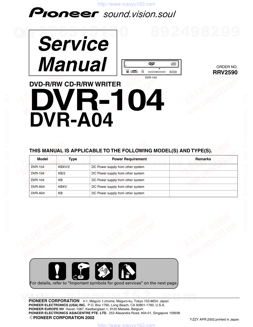
DVR-104
RRV2590
DVD-R/RW CD-R/RW WRITER
DVR-104
DVR-A04
THIS MANUAL IS APPLICABLE TO THE FOLLOWING MODEL(S) AND TYPE(S).
Model
Type
Power Requirement
Remarks
DVR-104
KBXV/2
DC Power supply from other system
DVR-104
KB/2
DC Power supply from other system
DVR-104
KB
DC Power supply from other system
DVR-A04
KBXV
DC Power supply from other system
DVR-A04
KB
DC Power supply from other system
For details, refer to "Important symbols for good services" on the next page.
T-ZZY APR.2002.printed in Japan
www. xiaoyu163. com
QQ 376315150
9
9
2
8
9
4
2
9
8
TEL 13942296513
9
9
2
8
9
4
2
9
8
0
5
1
5
1
3
6
7
3
Q
Q
TEL 13942296513 QQ 376315150 892498299
TEL 13942296513 QQ 376315150 892498299
http://www.xiaoyu163.com
DVR-104
2
1
2
3
4
1
2
3
4
C
D
F
A
B
E
SAFTY INFORMATION
IMPORTANT
THIS PIONEER APPARATUS CONTAINS
LASER OF CLASS 1.
SERVICING OPERATION OF THE APPARATUS
SHOULD BE DONE BY A SPECIALLY
INSTRUCTED PERSON.
LASER DIODE CHARACTERISTICS
MAXIMUM OUTPUT POWER: 7 mw
WAVELENGTH: 650 nm (DVD) , 780 nm (CD-ROM)
This service manual is intended for qualified service technicians; it is not meant for the
casual do-it-yourselfer. Qualified technicians have the necessary test equipment and tools, and have
been trained to properly and safely repair complex products such as those covered by this manual.
Improperly performed repairs can adversely affect the safety and reliability of the product and may
void the warranty. If you are not qualified to perform the repair of this product properly and safely,
you should not risk trying to do so and refer the repair to a qualified service technician.
WARNING
This product contains lead in solder and certain electrical parts contain chemicals which are known to the state of California to
cause cancer, birth defects or other reproductive harm.
Health & Safety Code Section 25249.6 – Proposition 65
(DRW2080)
DRW2080
(DRW2069)
DRW2069
1. The ON/OFF(ON:low level,OFF:high level) status of the
CLAMP signals for detcting the loading state are detected
by the drive CPUs, and the design prevents
laser diode oscillation when the CLAMP signal turns OFF.
In normal operation, if no disc is clamped, the laser diode
oscillation is disabled.
However, the interlock does not always operate in the test
mode. *
2. When the cover is opened, close viewing of the objective
lens with the naked eye will cause exposure to a Class 3A
laser beam.
Additional Laser Caution
* Refer to pages 38.
DVR-104/KB, DVR-104/KB/2 and DVR-A04/KB only
DVR-104/KBXV/2 and DVR-A04/KBXV only
www. xiaoyu163. com
QQ 376315150
9
9
2
8
9
4
2
9
8
TEL 13942296513
9
9
2
8
9
4
2
9
8
0
5
1
5
1
3
6
7
3
Q
Q
TEL 13942296513 QQ 376315150 892498299
TEL 13942296513 QQ 376315150 892498299
http://www.xiaoyu163.com
DVR-104
3
5
6
7
8
5
6
7
8
C
D
F
A
B
E
[ Important symbols for good services ]
In this manual, the symbols shown-below indicate that adjustments, settings or cleaning should be made securely.
When you find the procedures bearing any of the symbols, be sure to fulfill them:
2. Adjustments
To keep the original performances of the product, optimum adjustments or specification confirmation is indispensable.
In accordance with the procedures or instructions described in this manual, adjustments should be performed.
3. Cleaning
For optical pickups, tape-deck heads, lenses and mirrors used in projection monitors, and other parts requiring cleaning,
proper cleaning should be performed to restore their performances.
5. Lubricants, glues, and replacement parts
Appropriately applying grease or glue can maintain the product performances. But improper lubrication or applying
glue may lead to failures or troubles in the product. By following the instructions in this manual, be sure to apply the
prescribed grease or glue to proper portions by the appropriate amount.For replacement parts or tools, the prescribed
ones should be used.
4. Shipping mode and shipping screws
To protect the product from damages or failures that may be caused during transit, the shipping mode should be set or
the shipping screws should be installed before shipping out in accordance with this manual, if necessary.
1. Product safety
You should conform to the regulations governing the product (safety, radio and noise, and other regulations), and
should keep the safety during servicing by following the safety instructions described in this manual.
www. xiaoyu163. com
QQ 376315150
9
9
2
8
9
4
2
9
8
TEL 13942296513
9
9
2
8
9
4
2
9
8
0
5
1
5
1
3
6
7
3
Q
Q
TEL 13942296513 QQ 376315150 892498299
TEL 13942296513 QQ 376315150 892498299
http://www.xiaoyu163.com
DVR-104
4
1
2
3
4
1
2
3
4
C
D
F
A
B
E
CONTENTS
SAFTY INFORMATION . . . . . . . . . . . . . . . . . . . . . . . . . . . . . . . . . . . . . . . . . . . . . 2
1. SPECIFICATIONS . . . . . . . . . . . . . . . . . . . . . . . . . . . . . . . . . . . . . . . . . . . . . . . 5
2. EXPLODED VIEWS AND PARTS LIST . . . . . . . . . . . . . . . . . . . . . . . . . . . . . . . . . . . . 6
2.1 PACKING . . . . . . . . . . . . . . . . . . . . . . . . . . . . . . . . . . . . . . . . . . . . . . . . . 6
2.2 EXTERIOR (1/2) SECTION . . . . . . . . . . . . . . . . . . . . . . . . . . . . . . . . . . . . . . . . 8
2.3 EXTERIOR (2/2) SECTION . . . . . . . . . . . . . . . . . . . . . . . . . . . . . . . . . . . . . . . 10
2.4 TRAVERSE MECHANISM ASSY-S . . . . . . . . . . . . . . . . . . . . . . . . . . . . . . . . . . . 12
3. BLOCK DIAGRAM AND SCHEMATIC DIAGRAM . . . . . . . . . . . . . . . . . . . . . . . . . . . . . . 14
3.1 BLOCK DIAGRAM . . . . . . . . . . . . . . . . . . . . . . . . . . . . . . . . . . . . . . . . . . . . 14
3.2 OVERALL WIRING DIAGRAM. . . . . . . . . . . . . . . . . . . . . . . . . . . . . . . . . . . . . . 16
3.3 DVR R4 MAIN ASSY (1/5) . . . . . . . . . . . . . . . . . . . . . . . . . . . . . . . . . . . . . . . . 18
3.4 DVR R4 MAIN ASSY (2/5) . . . . . . . . . . . . . . . . . . . . . . . . . . . . . . . . . . . . . . . . 20
3.5 DVR R4 MAIN ASSY (3/5) . . . . . . . . . . . . . . . . . . . . . . . . . . . . . . . . . . . . . . . . 22
3.6 DVR R4 MAIN ASSY (4/5) . . . . . . . . . . . . . . . . . . . . . . . . . . . . . . . . . . . . . . . . 24
3.7 DVR R4 MAIN ASSY (5/5) . . . . . . . . . . . . . . . . . . . . . . . . . . . . . . . . . . . . . . . . 26
4. PCB CONNECTION DIAGRAM . . . . . . . . . . . . . . . . . . . . . . . . . . . . . . . . . . . . . . . 31
4.1 DVR R4 MAIN ASSY. . . . . . . . . . . . . . . . . . . . . . . . . . . . . . . . . . . . . . . . . . . 32
5. PCB PARTS LIST . . . . . . . . . . . . . . . . . . . . . . . . . . . . . . . . . . . . . . . . . . . . . . 34
6. ADJUSTMENT . . . . . . . . . . . . . . . . . . . . . . . . . . . . . . . . . . . . . . . . . . . . . . . . 36
6.1 TEST MODE . . . . . . . . . . . . . . . . . . . . . . . . . . . . . . . . . . . . . . . . . . . . . . . 38
6.1.1 Sending Test Mode Commands . . . . . . . . . . . . . . . . . . . . . . . . . . . . . . . . . . . . 38
6.1.2 Disc Selection . . . . . . . . . . . . . . . . . . . . . . . . . . . . . . . . . . . . . . . . . . . . . 38
6.2 ADJUSTMENT. . . . . . . . . . . . . . . . . . . . . . . . . . . . . . . . . . . . . . . . . . . . . . 39
6.2.1 VCO Free-running Adjustment. . . . . . . . . . . . . . . . . . . . . . . . . . . . . . . . . . . . . 39
6.2.2 BPF Center frequency Adjustment / Wobull Dely Adjustment . . . . . . . . . . . . . . . . . . . . . 39
6.2.3 Power Adjustment . . . . . . . . . . . . . . . . . . . . . . . . . . . . . . . . . . . . . . . . . . . 40
6.2.4 Radial Tilt Circuit Adjustment . . . . . . . . . . . . . . . . . . . . . . . . . . . . . . . . . . . . . 43
6.2.5 Focus Position Adjustment. . . . . . . . . . . . . . . . . . . . . . . . . . . . . . . . . . . . . . . 44
6.2.6 Playback Ability Confirmation . . . . . . . . . . . . . . . . . . . . . . . . . . . . . . . . . . . . . 45
6.2.7 Recording Ability Confirmation. . . . . . . . . . . . . . . . . . . . . . . . . . . . . . . . . . . . . 46
6.3 Release the Test mode. . . . . . . . . . . . . . . . . . . . . . . . . . . . . . . . . . . . . . . . . . 46
7. GENERAL INFORMATION. . . . . . . . . . . . . . . . . . . . . . . . . . . . . . . . . . . . . . . . . . 47
7.1 DIAGNOSIS . . . . . . . . . . . . . . . . . . . . . . . . . . . . . . . . . . . . . . . . . . . . . . . 47
7.1.1 DISASSEMBLY . . . . . . . . . . . . . . . . . . . . . . . . . . . . . . . . . . . . . . . . . . . . 47
7.1.2 CLEANING. . . . . . . . . . . . . . . . . . . . . . . . . . . . . . . . . . . . . . . . . . . . . . . 49
7.2 PARTS . . . . . . . . . . . . . . . . . . . . . . . . . . . . . . . . . . . . . . . . . . . . . . . . . . 50
7.2.1 IC . . . . . . . . . . . . . . . . . . . . . . . . . . . . . . . . . . . . . . . . . . . . . . . . . . . 50
8. PANEL FACILITIES . . . . . . . . . . . . . . . . . . . . . . . . . . . . . . . . . . . . . . . . . . . . . 68
www. xiaoyu163. com
QQ 376315150
9
9
2
8
9
4
2
9
8
TEL 13942296513
9
9
2
8
9
4
2
9
8
0
5
1
5
1
3
6
7
3
Q
Q
TEL 13942296513 QQ 376315150 892498299
TEL 13942296513 QQ 376315150 892498299
http://www.xiaoyu163.com
DVR-104
5
5
6
7
8
5
6
7
8
C
D
F
A
B
E
1. SPECIFICATIONS
[Setting]
This drive is Horizontal and Vertical Use.
[Disc Size]
• 12 cm (4.72”) / 8 cm (3.15”)*
*8 cm (3.15") discs cannot be used at upright position.
[Data Transfer Rate]
Data Read (Sustained)
DVD Max. 8,100 KBytes/sec.
CD Max. 3,600 KBytes/sec. (10.3 – 24X CAV Mode over 16 block transfer)
Data Write (Sustained)
DVD Max. 2,700 KBytes/sec. (2X DVD-R)
CD Max. 1,200 KBytes/sec. (8X CD-R)
Host Interface specification
PIO Mode 4, Multi word DMA Mode 2 16.6 Mbytes/sec.
Ultra DMA mode 2 33.3 MBytes/sec.
• The data transfer rate may not be output due to disc conditions (scratches, etc.).
[Access Time/ Seek Time]
Access time (Random average)
DVD-ROM 200 ms CD-ROM 180 ms
Seek time (Random average)
DVD-ROM 150 ms CD-ROM 130 ms
[Audio Characteristic]
Line Out 0.7 ± 0.5 Vrms (at 10 kΩ load)
Headphone Out 0.6 ± 0.5 Vrms (at 32 Ω load)
[Others]
Power Supply
DC +12 V, 0.7 A
DC +5 V, 1.4 A
Dimensions
148 (W) x 42.3 (H) x 197.7 (D) mm
(including front panel)
5-27/32 (W) x 1-11/16 (H) x 7-25/32 (D) in.
Weight
1.2 kg (2.65 lb)
Operation temperature
+5°C to +45°C (41°F to 113°F)
Operation humidity
5% to 85% (no condensation)
Storage temperature
– 40°C to +60°C (– 40°F to 140°F)
Storage humidity
5% to 90% (no condensation)
[Accessories] (DVR-A04 only)
Push Rod
x1
Short-circuit socket
x2
Audio cable
x1
Mounting screw
x4
Operating instructions
x1
NOTE:
• Specifications and design subject to possible modifications without notice, due to improvements.
[DVR-104 and DVR-A04]
Mounting screw x4
(AMZ30P060FMC)
Short-circuit socket x2
(DKX1042)
Audio cable x1
(DKP3369)
Push Rod
(DEX1008)
Accessories
(DVR-A04 only)
www. xiaoyu163. com
QQ 376315150
9
9
2
8
9
4
2
9
8
TEL 13942296513
9
9
2
8
9
4
2
9
8
0
5
1
5
1
3
6
7
3
Q
Q
TEL 13942296513 QQ 376315150 892498299
TEL 13942296513 QQ 376315150 892498299
http://www.xiaoyu163.com
DVR-104
6
1
2
3
4
1
2
3
4
C
D
F
A
B
E
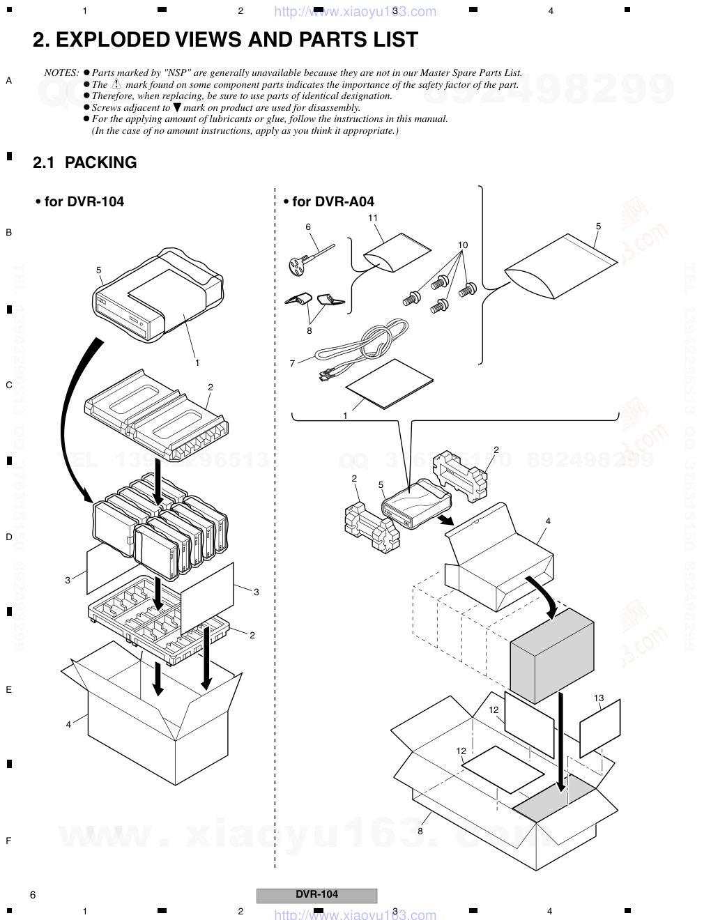
2. EXPLODED VIEWS AND PARTS LIST
2.1 PACKING
Parts marked by "NSP" are generally unavailable because they are not in our Master Spare Parts List.
The mark found on some component parts indicates the importance of the safety factor of the part.
Therefore, when replacing, be sure to use parts of identical designation.
Screws adjacent to mark on product are used for disassembly.
For the applying amount of lubricants or glue, follow the instructions in this manual.
(In the case of no amount instructions, apply as you think it appropriate.)
NOTES:
13
12
12
8
5
11
10
• for DVR-104
• for DVR-A04
6
8
7
1
2
1
5
3
4
3
2
5
4
2
2
www. xiaoyu163. com
QQ 376315150
9
9
2
8
9
4
2
9
8
TEL 13942296513
9
9
2
8
9
4
2
9
8
0
5
1
5
1
3
6
7
3
Q
Q
TEL 13942296513 QQ 376315150 892498299
TEL 13942296513 QQ 376315150 892498299
http://www.xiaoyu163.com
DVR-104
7
5
6
7
8
5
6
7
8
C
D
F
A
B
E
PACKING parts List
(2) CONTRAST TABLE
DVR-104/KB/2, DVR-104/KB, DVR-A04/KBXV, DVR-A04/KB and DVR-104/KBXV2 are constructed the same
except for the following.
Mark No.
Description
Part No.
1
Operating Instructions
See Contrast table (2)
2
Pad
See Contrast table (2)
3
Support Board
See Contrast table (2)
4
Packing Case
See Contrast table (2)
NSP 5
Polyethylene Bag
See Contrast table (2)
6
Push Rod
See Contrast table (2)
7
Audio Cable
See Contrast table (2)
8
Short-circuit Socket
See Contrast table (2)
9
Master Carton A04
See Contrast table (2)
10
Mounting Screw
See Contrast table (2)
NSP 11
Polyethylene Bag
See Contrast table (2)
12
Spacer1
See Contrast table (2)
13
Spacer2
See Contrast table (2)
Mark No.
Description
Part No.
Mark
NO
Symbol and Description
DVR-104/KBXV/2
DVR-104/KB/2
DVR-104/KB
DVR-A04/KBXV
DVR-A04/KB
1
Operating Instructions R4
(English/French/German)
DRC1177
DRC1169
DRC1169
Not used
Not used
1
Operating Instructions R4
(English/French/German/Italian/
Dutch/ Spanish/Japanese)
Not used
Not used
Not used
DRC1180
DRC1174
2
Pad R4XCN
DHA1539
Not used
Not used
Not used
Not used
2
Pad R4
Not used
DHA1532
DHA1532
Not used
Not used
2
Pad A04
Not used
DHA1532
DHA1532
DHA1545
DHA1450
3
Support Board
DHG2144
DHG2141
DHG2141
Not used
Not used
4
Packing Case XV/2
DHG2233
Not used
Not used
Not used
Not used
4
Packing Case R4/2
Not used
DHG2243
Not used
Not used
Not used
4
Packing Case R4
Not used
Not used
DHG2178
Not used
Not used
4
Packing Case A04
Not used
Not used
Not used
DHG2217
DHG2202
NSP
5
Polyethylene Bag
DHL1119
Not used
Not used
DHL1119
Not used
NSP
5
Polyethylene Bag
(235 x 320 x 0.03)
Not used
Z21-018
Z21-018
Not used
Z21-018
6
Push Rod
Not used
Not used
Not used
DEX1008
DEX1008
7
Audio Cable
Not used
Not used
Not used
DKP3369
DKP3369
8
Short-circuit Socket
Not used
Not used
Not used
DKX1042
DKX1042
9
Master Carton A04
Not used
Not used
Not used
DHG2218
DHG2203
10 Mounting Screw
Not used
Not used
Not used
AMZ30P060FMC AMZ30P060FMC
NSP
11
Polyethylene Bag
Not used
Not used
Not used
DHL1120
DHL1089
12
Spacer 1
Not used
Not used
Not used
Not used
DHG2275
13 Spacer 2
Not used
Not used
Not used
Not used
DHG2276
www. xiaoyu163. com
QQ 376315150
9
9
2
8
9
4
2
9
8
TEL 13942296513
9
9
2
8
9
4
2
9
8
0
5
1
5
1
3
6
7
3
Q
Q
TEL 13942296513 QQ 376315150 892498299
TEL 13942296513 QQ 376315150 892498299
http://www.xiaoyu163.com
DVR-104
8
1
2
3
4
1
2
3
4
C
D
F
A
B
E
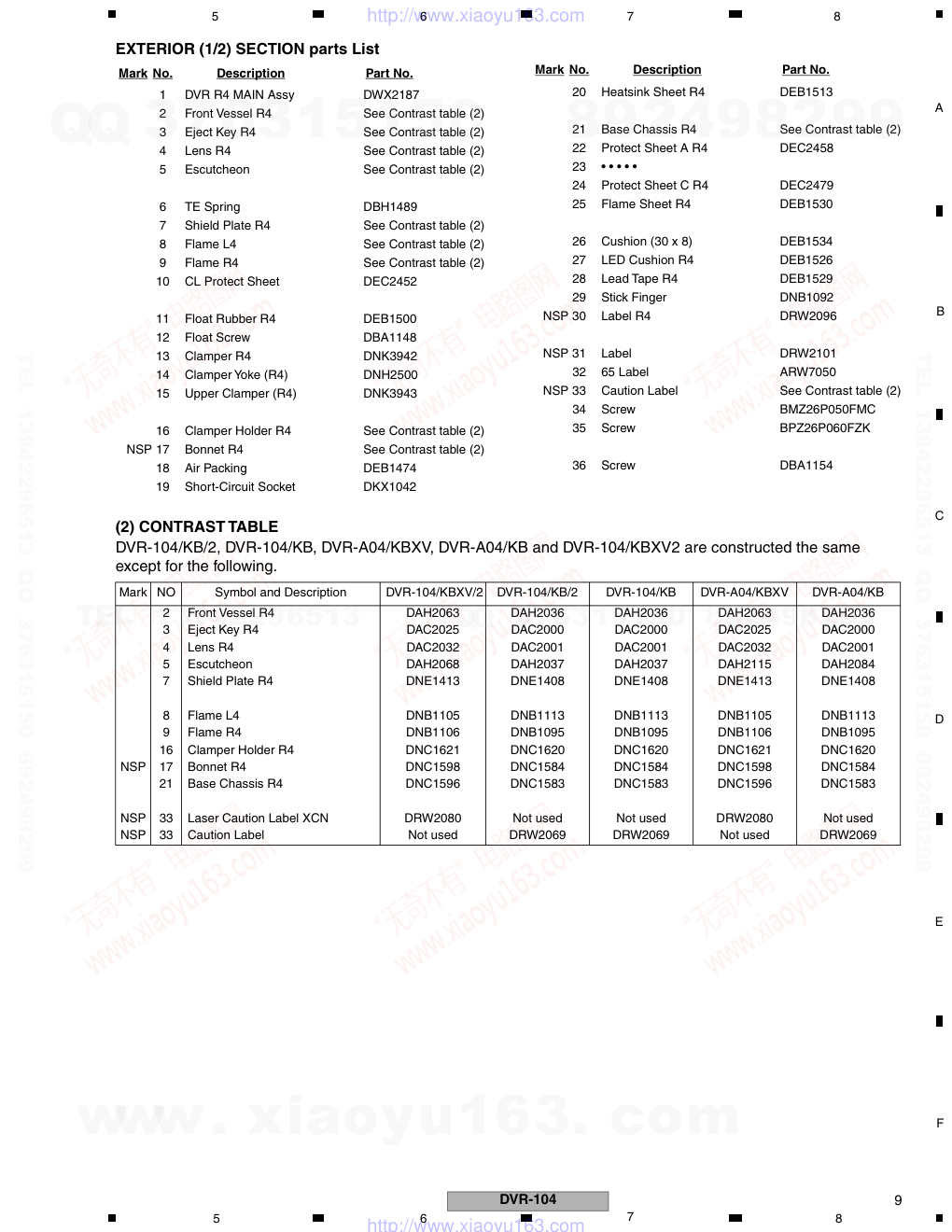
2.2 EXTERIOR (1/2) SECTION
A
A
B
B
C
C
D
D
E
E
F
F
B
B
A
A
17
34
34
30
10
14
13
8
25
11
36
7
2
5
12
11
9
1
21
26
27
28
20
4
3
6
6
12
15
35
24
22
24
35
16
Refer to
"2.3 EXTERIOR SECTION (2/2)".
33
29
32
18
A
34
34
34
19
34
31
CONTACT SIDE
NON-CONTACT
SIDE
www. xiaoyu163. com
QQ 376315150
9
9
2
8
9
4
2
9
8
TEL 13942296513
9
9
2
8
9
4
2
9
8
0
5
1
5
1
3
6
7
3
Q
Q
TEL 13942296513 QQ 376315150 892498299
TEL 13942296513 QQ 376315150 892498299
http://www.xiaoyu163.com
DVR-104
9
5
6
7
8
5
6
7
8
C
D
F
A
B
E
EXTERIOR (1/2) SECTION parts List
(2) CONTRAST TABLE
DVR-104/KB/2, DVR-104/KB, DVR-A04/KBXV, DVR-A04/KB and DVR-104/KBXV2 are constructed the same
except for the following.
Mark No.
Description
Part No.
1
DVR R4 MAIN Assy
DWX2187
2
Front Vessel R4
See Contrast table (2)
3
Eject Key R4
See Contrast table (2)
4
Lens R4
See Contrast table (2)
5
Escutcheon
See Contrast table (2)
6
TE Spring
DBH1489
7
Shield Plate R4
See Contrast table (2)
8
Flame L4
See Contrast table (2)
9
Flame R4
See Contrast table (2)
10
CL Protect Sheet
DEC2452
11
Float Rubber R4
DEB1500
12
Float Screw
DBA1148
13
Clamper R4
DNK3942
14
Clamper Yoke (R4)
DNH2500
15
Upper Clamper (R4)
DNK3943
16
Clamper Holder R4
See Contrast table (2)
NSP 17
Bonnet R4
See Contrast table (2)
18
Air Packing
DEB1474
19
Short-Circuit Socket
DKX1042
20
Heatsink Sheet R4
DEB1513
21
Base Chassis R4
See Contrast table (2)
22
Protect Sheet A R4
DEC2458
23
• • • • •
24
Protect Sheet C R4
DEC2479
25
Flame Sheet R4
DEB1530
26
Cushion (30 x 8)
DEB1534
27
LED Cushion R4
DEB1526
28
Lead Tape R4
DEB1529
29
Stick Finger
DNB1092
NSP 30
Label R4
DRW2096
NSP 31
Label
DRW2101
32
65 Label
ARW7050
NSP 33
Caution Label
See Contrast table (2)
34
Screw
BMZ26P050FMC
35
Screw
BPZ26P060FZK
36
Screw
DBA1154
Mark No.
Description
Part No.
Mark NO
Symbol and Description
DVR-104/KBXV/2
DVR-104/KB/2
DVR-104/KB
DVR-A04/KBXV
DVR-A04/KB
2
Front Vessel R4
DAH2063
DAH2036
DAH2036
DAH2063
DAH2036
3
Eject Key R4
DAC2025
DAC2000
DAC2000
DAC2025
DAC2000
4
Lens R4
DAC2032
DAC2001
DAC2001
DAC2032
DAC2001
5
Escutcheon
DAH2068
DAH2037
DAH2037
DAH2115
DAH2084
7
Shield Plate R4
DNE1413
DNE1408
DNE1408
DNE1413
DNE1408
8
Flame L4
DNB1105
DNB1113
DNB1113
DNB1105
DNB1113
9
Flame R4
DNB1106
DNB1095
DNB1095
DNB1106
DNB1095
16
Clamper Holder R4
DNC1621
DNC1620
DNC1620
DNC1621
DNC1620
NSP
17
Bonnet R4
DNC1598
DNC1584
DNC1584
DNC1598
DNC1584
21
Base Chassis R4
DNC1596
DNC1583
DNC1583
DNC1596
DNC1583
NSP
33
Laser Caution Label XCN
DRW2080
Not used
Not used
DRW2080
Not used
NSP
33
Caution Label
Not used
DRW2069
DRW2069
Not used
DRW2069
www. xiaoyu163. com
QQ 376315150
9
9
2
8
9
4
2
9
8
TEL 13942296513
9
9
2
8
9
4
2
9
8
0
5
1
5
1
3
6
7
3
Q
Q
TEL 13942296513 QQ 376315150 892498299
TEL 13942296513 QQ 376315150 892498299
http://www.xiaoyu163.com
DVR-104
10
1
2
3
4
1
2
3
4
C
D
F
A
B
E
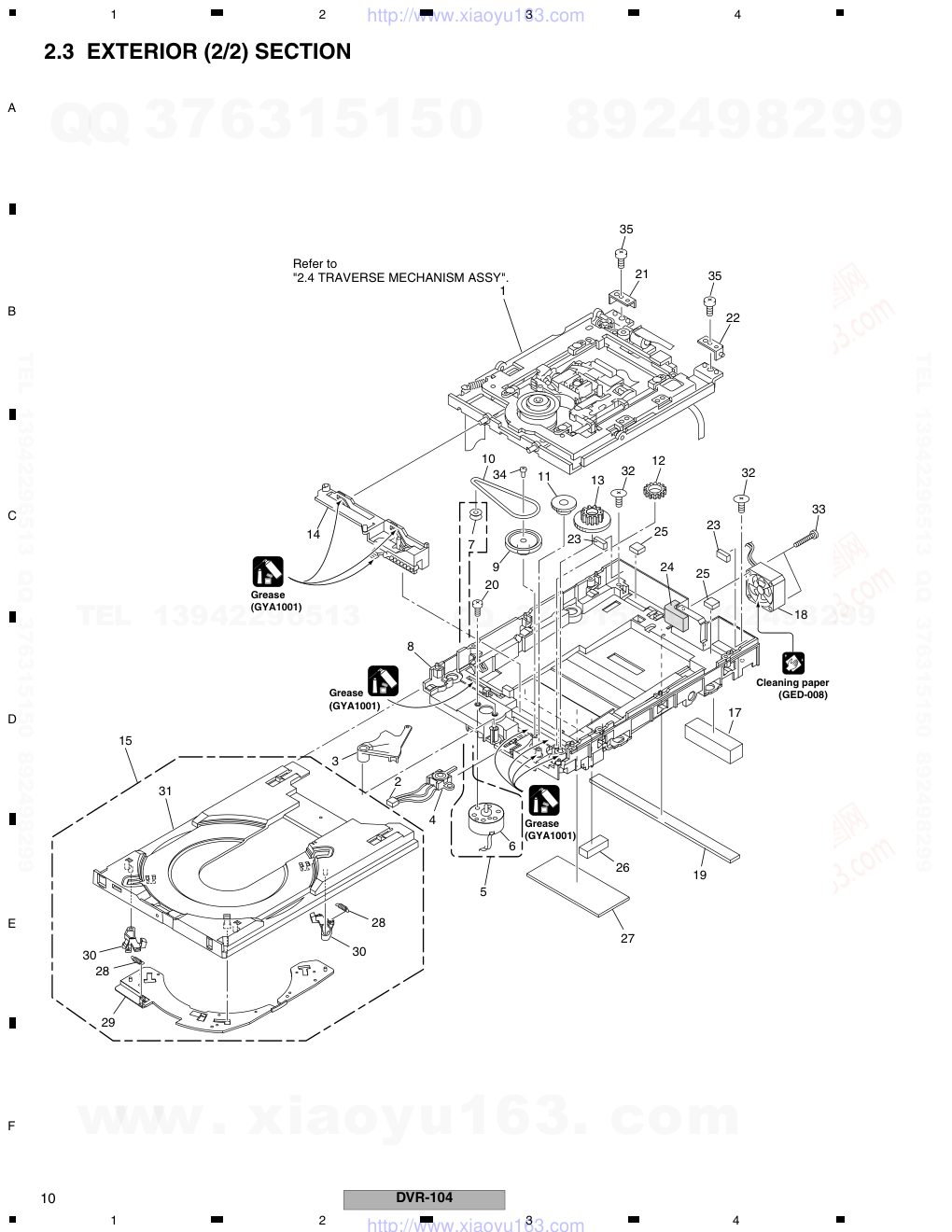
2.3 EXTERIOR (2/2) SECTION
35
22
21
1
12
18
19
8
3
2
15
30
30
28
28
29
31
6
5
33
13
11
10
34
7
9
20
14
32
32
23
23
25
25
24
4
35
27
17
26
Refer to
"2.4 TRAVERSE MECHANISM ASSY".
Grease
(GYA1001)
Grease
(GYA1001)
Grease
(GYA1001)
Cleaning paper
(GED-008)
www. xiaoyu163. com
QQ 376315150
9
9
2
8
9
4
2
9
8
TEL 13942296513
9
9
2
8
9
4
2
9
8
0
5
1
5
1
3
6
7
3
Q
Q
TEL 13942296513 QQ 376315150 892498299
TEL 13942296513 QQ 376315150 892498299
http://www.xiaoyu163.com
DVR-104
11
5
6
7
8
5
6
7
8
C
D
F
A
B
E
EXTERIOR (2/2) SECTION parts List
(2) CONTRAST TABLE
DVR-104/KB/2, DVR-104/KB, DVR-A04/KBXV, DVR-A04/KB and DVR-104/KBXV2 are constructed the same
except for the following.
Mark No.
Description
Part No.
1
Traverse Mechanism Assy-S
See Contrast table (2)
2
Connector Assy (3P)
DKP3544
3
Eject Lever R4
DNK3932
4
Lever Switch
DSK1001
5
Loading Motor Assy
DXX2503
NSP 6
Loading Motor R4
DXM1168
7
Motor Pulley
PNW1634
NSP 8
Loading Base R4
See Contrast table (2)
9
R4 Gear Pulley
DNK3972
10
Rubber Belt R4
DEB1523
11
R4 Gear A
DNK3935
12
R4 Gear C
DNK3933
13
R4 Gear B
DNK3934
14
Clamp Cam R4
DNK4034
15
Tray Assy
See Contrast table (2)
16
• • • • •
17
Spacer
DEB1482
18
Fan Motor R4
DXM1169
19
Air Packing
DEB1474
20
Screw
JGZ17P030FMC
21
Joint L
See Contrast table (2)
22
Joint R
See Contrast table (2)
23
Tray Cushion
DEB1512
24
Air Cushion S2
DEB1533
25
Cushion
DEB1525
26
Cushion (30 x 8)
DEB1534
27
Heatsink Sheet R4
DEB1514
28
Lock Spring
DBH1490
NSP 29
Link Plate
DNK3937
NSP 30
Disc Hook
DNK3938
NSP 31
Tray R4
DNK4050
32
Screw
DBA1165
33
Screw (2.6 x 15)
DBA1168
34
Screw (1.7P)
DBA1167
35
Screw
BMZ26P050FM
Mark No.
Description
Part No.
Mark NO
Symbol and Description
DVR-104/KBXV/2
DVR-104/KB/2
DVR-104/KB
DVR-A04/KBXV
DVR-A04/KB
1
Traverse Mechanism Assy-S
DXX2511
DXX2511
DXX2504
DXX2511
DXX2504
NSP
8
Loading Base R4
DNK3979
DNK3930
DNK3930
DNK3979
DNK3930
15
Tray Assy
DXA1940
DXA1932
DXA1932
DXA1940
DXA1932
21
Joint L
DNB1116
DNB1114
DNB1114
DNB1116
DNB1114
22
Joint R
DNB1117
DNB1115
DNB1115
DNB1117
DNB1115
www. xiaoyu163. com
QQ 376315150
9
9
2
8
9
4
2
9
8
TEL 13942296513
9
9
2
8
9
4
2
9
8
0
5
1
5
1
3
6
7
3
Q
Q
TEL 13942296513 QQ 376315150 892498299
TEL 13942296513 QQ 376315150 892498299
http://www.xiaoyu163.com
DVR-104
12
1
2
3
4
1
2
3
4
C
D
F
A
B
E
2.4 TRAVERSE MECHANISM ASSY-S
27
28
2
25
25
3
4
1
5
4
6
23
7
10
9
22
22
24
20
19
23
18
26
17
16
15
21
14
13
8
31
11
12
36
33
29
35
37
30
34
32
39
38
Cleaning liquid (GEM1004)
Cleaning paper (GED-008)
A
A
B
B
www. xiaoyu163. com
QQ 376315150
9
9
2
8
9
4
2
9
8
TEL 13942296513
9
9
2
8
9
4
2
9
8
0
5
1
5
1
3
6
7
3
Q
Q
TEL 13942296513 QQ 376315150 892498299
TEL 13942296513 QQ 376315150 892498299
http://www.xiaoyu163.com
DVR-104
13
5
6
7
8
5
6
7
8
C
D
F
A
B
E
TRAVERSE MECHANISM ASSY-S parts List
(2) CONTRAST TABLE
TRAVERSE MECHANISM ASSY-S (DXX2504) and (DXX2511) are constructed the same except for the following.
Mark No.
Description
Part No.
1
Tilt Base
See Contrast table (2)
2
Stopper R (R4)
DEB1502
3
Stopper F (R4)
DEB1501
4
Tilt Spring Y
DBH1479
5
Tilt Spring X
DBH1478
6
Stepping Motor
DXM1151
NSP 7
PICKUP Assy
See Contrast table (2)
8
Joint Spring (R4)
DBK1214
9
Main Shaft
DLA1921
10
Sub Shaft
DLA1923
11
Mechanism Base
See Contrast table (2)
12
Tilt Motor Assy
DXX2492
13
Warm
See Contrast table (2)
14
Tilt Motor
DXM1152
15
Tilt Gear A
See Contrast table (2)
16
Washer
WT21D040D050
17
Tilt Gear B
See Contrast table (2)
18
Tilt Cam
See Contrast table (2)
19
Spindle Motor (R4)
DXM1165
20
Screw
ZMR30H080FZK
21
Screw
BMZ26P040FMC
22
Screw
CMZ20P050FMC
23
Screw
PMA20P040FMC
24
Screw
DBA1121
25
Screw
DBA1149
26
Tilt Screw
DBA1163
27
Screw
DBA1158
28
Tilt Spring Z
DBH1482
29
Guide Spring (R4)
See Contrast table (2)
30
Cushion
DEB1484
31
Guide Blade (R4)
DNK3940
32
Cam Cover
See Contrast table (2)
33
Sub Guide (R4)
DNS1220
NSP 34
Tape (R4)
DEC2471
35
TAN Screw
VNL1761
36
Screw
PBZ20P040FMC
37
Screw
PBZ20P080FMC
38
Hold Spring (R4)
See Contrast table (2)
39
Stopper Screw
DBA1164
Mark No.
Description
Part No.
Mark
NO
Symbol and Description
DXX2511
DXX2504
1
Tilt Base
DNH2485
DNH2466
NSP
7
PICKUP Assy
OWY8016
OWY8001
11
Mechanism Base
DNH2509
DNH2501
13
Warm
DNK3899
DNK3825
15
Tilt Gear A
DNK3900
DNK3826
17
Tilt Gear B
DNK3901
DNK3827
18
Tilt Cam
DNK3902
DNK3828
29
Guide Spring (R4)
DBK1218
DBK1215
32
Cam Cover
DNK3903
DNK3863
38
Hold Spring (R4)
DBK1217
DBK1213
www. xiaoyu163. com
QQ 376315150
9
9
2
8
9
4
2
9
8
TEL 13942296513
9
9
2
8
9
4
2
9
8
0
5
1
5
1
3
6
7
3
Q
Q
TEL 13942296513 QQ 376315150 892498299
TEL 13942296513 QQ 376315150 892498299
http://www.xiaoyu163.com
DVR-104
14
1
2
3
4
1
2
3
4
C
D
F
A
B
E
3. BLOCK DIAGRAM AND SCHEMATIC DIAGRAM
3.1 BLOCK DIAGRAM
DVR R4 MAIN ASSY
A
Discrete
TILT ER
THERMO
SENSOR
FRONT
MONITOR
DIODE
CD
HOLOGRAM
Laser Diode
ACTUATOR
4P CONNECTOR
CN803
CN802
CN801
(C)
(D)
(D)
(D)
(D)
(D)
(D)
(D)
(C)
(C)
(C)
(C)
(C)
(C)
VR1
VR2
DVD-PB
PW Adj.
CD-PB PW Adj.
(S)
(S)
(SP)
(SP)
(SP)
(SP)
(SP)
(SP)
(SP)
(T)
(L)
(L)
(L)
(T)
(T)
(S)
(T)
(L)
1,12
6- 9
6- 9
11-12
13-14
28-30
4- 5
23,24
31,32
17
16
15
38
10-11
18-21
10-13
47-48
6- 9
28
17
4
9
29
31
34
78
53
49
63
2
93
35
57
56
82
26
2
23,24
31,32
146-148
1
2
3, 4
14,17
37-40
4Mbit
TLAMP
LPPRD1 LPPDFR
LPPWR LPPDFW
RF: 116
TE: 56
FE: 60
CN301
BUFFER
BUFFER
www. xiaoyu163. com
QQ 376315150
9
9
2
8
9
4
2
9
8
TEL 13942296513
9
9
2
8
9
4
2
9
8
0
5
1
5
1
3
6
7
3
Q
Q
TEL 13942296513 QQ 376315150 892498299
TEL 13942296513 QQ 376315150 892498299
http://www.xiaoyu163.com
DVR-104
15
5
6
7
8
5
6
7
8
C
D
F
A
B
E
JA201
D/A CONVERTER
CN401
CN402
POWER
SUPPLY
SECTION
: PB SIGNAL ROUTE
: CD PB RF SIGNAL ROUTE
: DVD PB RF SIGNAL ROUTE
(C)
(PB)
(C)
(S)
(T)
(D)
: LPP SIGNAL ROUTE
(D)
: CD REC SIGNAL ROUTE
: DVD REC SIGNAL ROUTE
: TE SIGNAL ROUTE
: FE SIGNAL ROUTE
: TILT MOTOR SIGNAL
: SLIDER MOTOR SIGNAL
(SP)
: SPINDLE MOTOR SIGNAL
: CD TE SIGNAL ROUTE
: DVD TE SIGNAL ROUTE
(C)
(D)
(PB)
(REC)
(PB)
(PB)
(PB)
(PB)
(PB)
(PB)
(PB)
(PB)
(D)
(D)
VC701
VC702
1st PLL VCO Adj.
2nd PLL VCO Adj.
(SP)
(SP)
(SP)
(SP)
(S)
(T)
(S)
(T)
142
143
148
141
129
136
181
177
108
102
39
7
146,147
58,59
209,210
211,212
215
13-15
1-3, 16
146-148
100,101
109,110
159-163
111-114
132,133
150-153
16.93M
RF, TE, FE
RF: 116
TE: 140
FE: 139
LPPRD1 LPPDFR
LPPWR LPPDFW
51
52
53
54
www. xiaoyu163. com
QQ 376315150
9
9
2
8
9
4
2
9
8
TEL 13942296513
9
9
2
8
9
4
2
9
8
0
5
1
5
1
3
6
7
3
Q
Q
TEL 13942296513 QQ 376315150 892498299
TEL 13942296513 QQ 376315150 892498299
http://www.xiaoyu163.com
DVR-104
16
1
2
3
4
1
2
3
4
C
D
F
A
B
E
3.2 OVERALL WIRING DIAGRAM
TILT MOTOR ASSY
(DXX2492)
SLIDER MOTOR
(DXM1151)
www. xiaoyu163. com
QQ 376315150
9
9
2
8
9
4
2
9
8
TEL 13942296513
9
9
2
8
9
4
2
9
8
0
5
1
5
1
3
6
7
3
Q
Q
TEL 13942296513 QQ 376315150 892498299
TEL 13942296513 QQ 376315150 892498299
http://www.xiaoyu163.com
DVR-104
17
5
6
7
8
5
6
7
8
C
D
F
A
B
E
LOADING MOTOR ASSY
(DXX2503)
SPINDLE MOTOR
(DXM1165)
DVR R4 MAIN ASSY
(DWX2187)
A
A 1/5 -5/5
TRAY OPEN
CLUMP UP
www. xiaoyu163. com
QQ 376315150
9
9
2
8
9
4
2
9
8
TEL 13942296513
9
9
2
8
9
4
2
9
8
0
5
1
5
1
3
6
7
3
Q
Q
TEL 13942296513 QQ 376315150 892498299
TEL 13942296513 QQ 376315150 892498299
http://www.xiaoyu163.com
DVR-104
18
1
2
3
4
1
2
3
4
C
D
F
A
B
E
3.3 DVR R4 MAIN ASSY (1/5)
1/5, 4/5
A
1/5
A
3/5
A
1/5
A
1/5
A
1/5
A
BTL DRIVER
CN101
1/5
A
1/5
A
1/5
A
A 1/5
2/5
A
1/5
A
1/5
A
3/5
A
3/5
A
3/5
A
1/5
A
1/5
A
1/5
A
3/5
A
1/5, 4/5
A
3/5
A
3/5
A
1/5
A
3/5
A
2/5
A
15
12
19
13
14
4
16
9
8
11
5 6a
18
10
20
7
6
1
17
2
(D)
(D)
(D)
(D)
(D)
(D)
(D)
(D)
(C)
(C)
(C)
(C)
(C)
(D)
(D)
(C)
(C)
(C)
(C)
(C)
(C)
(C)
(C)
(D)
(D)
(C)
(C)
(C)
(C)
(C)
(D)
(D)
(D)
(D)
(D)
(D)
(D)
(C)
(C)
(C)(D)
7b
7b
www. xiaoyu163. com
QQ 376315150
9
9
2
8
9
4
2
9
8
TEL 13942296513
9
9
2
8
9
4
2
9
8
0
5
1
5
1
3
6
7
3
Q
Q
TEL 13942296513 QQ 376315150 892498299
TEL 13942296513 QQ 376315150 892498299
http://www.xiaoyu163.com
DVR-104
19
5
6
7
8
5
6
7
8
C
D
F
A
B
E
CLAMP SW
DRIVER
DRIVER
CN601
2/5
A
DVR R4 MAIN ASSY
(DWX2187)
A 1/5
A 1/5
2/5
A
2/5
A
2/5
A
1/5, 3/5
A
4/5
A
4/5
A
4/5
A
4/5
A
5/5
A
1/5
A
1/5
A
5/5
A
5/5
A
1/5
A
2/5
A
2/5
A
2/5
A
2/5
A
2/5, 3/5
A
3/5
A
TRAY OPEN
TRAY CLAMP
1/5
A
1/5
A
2/5
A
3
: RF SIGNAL ROUTE
: CD PB RF SIGNAL ROUTE
: DVD PB RF SIGNAL ROUTE
(C)
(C)
(S)
(S)
(S)
(S)
(T)
(T)
(T)
(T)
(D)
(D)
: CD REC SIGNAL ROUTE
: DVD REC SIGNAL ROUTE
: TE SIGNAL ROUTE
: FE SIGNAL ROUTE
: CD TE SIGNAL ROUTE
: DVD TE SIGNAL ROUTE
(S)
(T)
: SLIDER MOTOR SIGNAL
(SP) : SLIDER MOTOR SIGNAL
: TILT MOTOR SIGNAL
: LPP SIGNAL ROUTE
(C)
(D)
BTL DRIVER
(SP)
www. xiaoyu163. com
QQ 376315150
9
9
2
8
9
4
2
9
8
TEL 13942296513
9
9
2
8
9
4
2
9
8
0
5
1
5
1
3
6
7
3
Q
Q
TEL 13942296513 QQ 376315150 892498299
TEL 13942296513 QQ 376315150 892498299
http://www.xiaoyu163.com
DVR-104
20
1
2
3
4
1
2
3
4
C
D
F
A
B
E
3.4 DVR R4 MAIN ASSY (2/5)
CN401
JA201
PHONES
2/5
A
1/5
A
4/5
A
1/5
A
AUDIO OUT
4/5
A
1/5
A
1/5
A
2/5
A
1/5
A
(at 10kΩ LOAD)
(at 32Ω LOAD)
A 2/5
1/5
A
1/5
A
4/5
A
3/5
A
1/5
A
1/5
A
1/5
A
(PB)
(PB)
(PB)
(PB)
(PB)
(PB)
(PB)
(PB)
www. xiaoyu163. com
QQ 376315150
9
9
2
8
9
4
2
9
8
TEL 13942296513
9
9
2
8
9
4
2
9
8
0
5
1
5
1
3
6
7
3
Q
Q
TEL 13942296513 QQ 376315150 892498299
TEL 13942296513 QQ 376315150 892498299
http://www.xiaoyu163.com
DVR-104
21
5
6
7
8
5
6
7
8
C
D
F
A
B
E
CN301
CN401
2/5
A
DVR R4 MAIN ASSY
(DWX2187)
A 2/5
A 2/5
3/5
A
1/5
A
3/5
A
1/5
A
CN401
: PB SIGNAL ROUTE
(PB)
: RF SIGNAL ROUTE
: REC SIGNAL ROUTE
: TE SIGNAL ROUTE
: FE SIGNAL ROUTE
www. xiaoyu163. com
QQ 376315150
9
9
2
8
9
4
2
9
8
TEL 13942296513
9
9
2
8
9
4
2
9
8
0
5
1
5
1
3
6
7
3
Q
Q
TEL 13942296513 QQ 376315150 892498299
TEL 13942296513 QQ 376315150 892498299
http://www.xiaoyu163.com
DVR-104
22
1
2
3
4
1
2
3
4
C
D
F
A
B
E
3.5 DVR R4 MAIN ASSY (3/5)
DVR R4 MAIN ASSY
(DWX2187)
A 3/5
A 3/5
2/5
A
1/5
A
1/5
A
1/5
A
2/5
A
1/5
A
1/5
A
4/5
A
4/5
A
4/5
A
1/5
A
4/5
A
4/5
A
2/5
A
3/5
A
1/5
A
1/5
A
2/5
A
BTL DRIVER
(SP) : SPINDLE MOTOR SIGNAL
(SP)
(SP)
www. xiaoyu163. com
QQ 376315150
9
9
2
8
9
4
2
9
8
TEL 13942296513
9
9
2
8
9
4
2
9
8
0
5
1
5
1
3
6
7
3
Q
Q
TEL 13942296513 QQ 376315150 892498299
TEL 13942296513 QQ 376315150 892498299
http://www.xiaoyu163.com
DVR-104
23
5
6
7
8
5
6
7
8
C
D
F
A
B
E
A 3/5
4/5
A
1/5
A
www. xiaoyu163. com
QQ 376315150
9
9
2
8
9
4
2
9
8
TEL 13942296513
9
9
2
8
9
4
2
9
8
0
5
1
5
1
3
6
7
3
Q
Q
TEL 13942296513 QQ 376315150 892498299
TEL 13942296513 QQ 376315150 892498299
http://www.xiaoyu163.com
DVR-104
24
1
2
3
4
1
2
3
4
C
D
F
A
B
E
3.6 DVR R4 MAIN ASSY (4/5)
DVR R4 MAIN ASSY
(DWX2187)
A 4/5
A 4/5
3/5
A
1/5
A
1/5
A
1/5
A
1/5
A
2/5, 4/5
A
1/5
A
1/5
A
1/5
A
CN801
SPINDLE MOTOR
TILT MOTOR ASSY
CN803
: TE SIGNAL ROUTE
: FE SIGNAL ROUTE
: SLIDER MOTOR SIGNAL
: LOADING MOTOR SIGNAL
(L)
(S)
: TILT MOTOR SIGNAL
(T)
: SPINDLE MOTOR SIGNAL
(SP)
(T)
(T)
(T)
(T)
(T)
(SP)
(SP)
(SP)
(SP)
(SP)
SPDL DRIVER
www. xiaoyu163. com
QQ 376315150
9
9
2
8
9
4
2
9
8
TEL 13942296513
9
9
2
8
9
4
2
9
8
0
5
1
5
1
3
6
7
3
Q
Q
TEL 13942296513 QQ 376315150 892498299
TEL 13942296513 QQ 376315150 892498299
http://www.xiaoyu163.com
DVR-104
25
5
6
7
8
5
6
7
8
C
D
F
A
B
E
CAUTION:FOR CONTINUED PROTECTION AGAINST RISK OF FIRE.
REPLACE ONLY WITH SAME TIME NO. ICP-S1.8, MFD BY
ROHM CO., LTD. FOR IC409.
A 4/5
1/5
A
2/5
A
2/5, 3/5
A
3/5
A
3/5
A
CN802
SLIDER MOTOR ASSY
LOADING MOTOR
CN401
CN402
POWER
SUPPLY
2/5
A
(L)
(S)
(S)
(S)
(S)
(S)
(S)
(S)
(S)
(L)
(L)
(L)
(L)
(S)
: The power supply is shown with the marked box.
www. xiaoyu163. com
QQ 376315150
9
9
2
8
9
4
2
9
8
TEL 13942296513
9
9
2
8
9
4
2
9
8
0
5
1
5
1
3
6
7
3
Q
Q
TEL 13942296513 QQ 376315150 892498299
TEL 13942296513 QQ 376315150 892498299
http://www.xiaoyu163.com
DVR-104
26
1
2
3
4
1
2
3
4
C
D
F
A
B
E
3.7 DVR R4 MAIN ASSY (5/5)
DVR R4 MAIN ASSY
(DWX2187)
A 5/5
A 5/5
1/5
A
1/5
A
www. xiaoyu163. com
QQ 376315150
9
9
2
8
9
4
2
9
8
TEL 13942296513
9
9
2
8
9
4
2
9
8
0
5
1
5
1
3
6
7
3
Q
Q
TEL 13942296513 QQ 376315150 892498299
TEL 13942296513 QQ 376315150 892498299
http://www.xiaoyu163.com
DVR-104
27
5
6
7
8
5
6
7
8
C
D
F
A
B
E
FOR FREE-RUN ADJ
FILTER CHECK
2nd PLL VCO
FREE-RUN ADJ
1st PLL VCO
FREE-RUN ADJ
FOR FREE-RUN ADJ
A 5/5
1/5
A
1/5
A
1/5
A
1/5
A
www. xiaoyu163. com
QQ 376315150
9
9
2
8
9
4
2
9
8
TEL 13942296513
9
9
2
8
9
4
2
9
8
0
5
1
5
1
3
6
7
3
Q
Q
TEL 13942296513 QQ 376315150 892498299
TEL 13942296513 QQ 376315150 892498299
http://www.xiaoyu163.com
DVR-104
28
1
2
3
4
1
2
3
4
C
D
F
A
B
E
R134 (DWBL)
V : 2V/div. H : 5µsec/div.
(Disc: DVD-R x1 speed)
(Wobble after BPF)
2
IC112-Pin 63 (AWOBBLE)
V : 500mV/div. H : 5µsec/div.
(Disc: DVD-R x2 speed)
(Wobble before BPF)
1
3
4
3
4
IC112-Pin 60 (PPALL)
8
IC112-Pin 56 (TE)
V : 2V/div. H : 2msec/div.
(Disc: DVD-R Trk open)
IC112-Pin 60 (PPALL)
IC112-Pin 56 (TE)
V : 2V/div. H : 2msec/div.
(Disc: DVD-R Trk close)
9
IC108-Pin 23 (AWBLI)
8
9
6
7
R134 (DWBL)
V : 2V/div. H : 5µsec/div.
(Disc: DVD-R x2 speed)
(Wobble after BPF)
IC108-Pin 23 (AWBLI)
6
7
IC112-Pin 64 (WOBBLE)
V : 2V/div. H : 5µsec/div.
(Disc: CD-R x4 speed)
(Wobble before BPF)
IC112-Pin 63 (AWOBBLE)
6a
7b
IC112-Pin 64 (WOBBLE)
V : 2V/div. H : 5µsec/div.
(Disc: CD-R x8 speed)
(Wobble before BPF)
IC112-Pin 63 (AWOBBLE)
6a
7b
IC112-Pin 56 (TE)
9
TP952 (TD_MON)
V : 500mV/div. H : 200µsec/div.
(Disc: DVD-R 1Trk Jump Forward)
10
R125 (XDVSTG)
V : 2V/div. H : 50nsec/div.
(Disc: DVD-R x1 speed)
IC108-Pin 26 (ALPPO)
V : 500mV/div. H : 5µsec/div.
(Disc: DVD-R x1 speed)
IC601-pin 134 (TZCOUT)
IC112-pin 54 (TECIN)
V : 2V/div. H : 200µsec/div.
(Disc: CD-ROM Trk open)
IC601-pin 134 (TZCOUT)
IC112-pin 54 (TECIN)
V : 2V/div. H : 200µsec/div.
(Disc: CD-ROM)
IC112-Pin 63 (AWOBBLE)
V : 500mV/div. H : 5µsec/div.
(Disc: DVD-R x1 speed)
(Wobble before BPF)
5
5
GND
GND
GND
GND
3
4
GND
GND
GND
3
4
7
6
GND
GND
7
6
GND
GND
7a
6a
GND
GND
7a
6a
9
8
GND
GND
GND
VSB1
VSB1
IC112-Pin 60 (PPALL)
8
IC112-Pin 56 (TE)
V : 2V/div. H : 2msec/div.
(Disc: CD-R Trk close)
9
9
8
VSB1
VSB1
9
10
GND
GND
IC112-Pin 56 (TE)
9
TP952 (TD_MON)
V : 500mV/div. H : 200µsec/div.
(Disc: CD-R 1Trk Jump Reverse)
10
9
10
GND
GND
IC112-Pin 56 (TE)
9
TP952 (TD_MON)
V : 500mV/div. H : 200µsec/div.
(Disc: DVD-R 1Trk Jump Forward)
10
9
10
GND
GND
IC112-Pin 56 (TE)
9
TP952 (TD_MON)
V : 500mV/div. H : 200µsec/div.
(Disc: CD-R 1Trk Jump Reverse)
10
9
10
GND
GND
9
8
VSB1
VSB1
IC112-Pin 60 (PPALL)
IC112-Pin 56 (TE)
V : 2V/div. H : 2msec/div.
(Disc: DVD-ROM Single Trk open)
9
8
VSB1
VSB1
IC112-Pin 60 (PPALL)
IC112-Pin 56 (TE)
V : 2V/div. H : 2msec/div.
(Disc: DVD-ROM Single Trk close)
9
8
VSB1
VSB1
IC112-Pin 60 (PPALL)
IC112-Pin 56 (TE)
V : 2V/div. H : 2msec/div.
(Disc: CD-R Trk open)
9
8
VSB1
VSB1
8
9
8
9
8
9
Waveforms (1/3)
Note: The encircled numbers denote measuring point in the schematic diagram. (Refer to pages 18 and 19)
www. xiaoyu163. com
QQ 376315150
9
9
2
8
9
4
2
9
8
TEL 13942296513
9
9
2
8
9
4
2
9
8
0
5
1
5
1
3
6
7
3
Q
Q
TEL 13942296513 QQ 376315150 892498299
TEL 13942296513 QQ 376315150 892498299
http://www.xiaoyu163.com
DVR-104
29
5
6
7
8
5
6
7
8
C
D
F
A
B
E
Waveforms (2/3)
9
IC112-Pin 99 (RFEQO)
V : 100mV/div. H : 50nsec/div.
(Disc: DVD-R x1 speed)
(AC mode)
IC112-Pin 99 (RFEQO)
V : 100mV/div. H : 50nsec/div.
(Disc: DVD-R x2 speed)
(AC mode)
IC112-Pin 99 (RFEQO)
V : 500mV/div. H : 2msec/div.
(Disc: CD-R x4 speed)
(AC mode)
IC112-Pin 99 (RFEQO)
V : 100mV/div. H : 50nsec/div.
(Disc: CD-R x8 speed)
(AC mode)
IC112-Pin 56 (TE)
V : 500mV/div. H : 10msec/div.
(Disc: DVD-ROM Single)
(Address 60000h - 50000h)
IC112-Pin 59 (FE)
V : 1V/div. H : 2msec/div.
(Disc: CD-R x8 speed Trk open)
IC112-Pin 116 (RFO)
V : 100mV/div. H : 50nsec/div.
(Disc: DVD-R x1 speed)
(AC mode)
13
11
13
13
13
VSB1
VSB1
9
IC112-Pin 56 (TE)
V : 500mV/div. H : 10msec/div.
(Disc: CD-ROM)
(Address 20min - 15min)
VSB1
11 IC112-Pin 59 (FE)
V : 500mV/div. H : 2msec/div.
(Disc: DVD-R x1 speed Trk open)
IC112-Pin 59 (FE)
V : 500mV/div. H : 2msec/div.
(Disc: DVD-R x2 speed Trk open)
IC112-Pin 59 (FE)
V : 1V/div. H : 2msec/div.
(Disc: CD-R x4 speed Trk open)
VSB1
11
VSB1
11
VSB1
IC112-Pin 99 (RFEQO)
V : 500mV/div. H : 1µsec/div.
13
IC112-Pin 90 (RECD)
V : 2V/div. H : 1µsec/div.
(Disc: DVD-R Unrecode-Recoded)
14
12
IC112-Pin 116 (RFO)
V : 100mV/div. H : 50nsec/div.
(Disc: DVD-R x2 speed)
(AC mode)
12
IC112-Pin 116 (RFO)
V : 100mV/div. H : 0.1µsec/div.
(Disc: CD-R x4 speed)
(AC mode)
12
IC112-Pin 116 (RFO)
V : 100mV/div. H : 50nsec/div.
(Disc: CD-R x8 speed)
(AC mode)
12
IC112-Pin 27 (PDMC)
V : 50mV/div. H : 50nsec/div
15
IC112-Pin 67 (SHAPCR)
V : 200mV/div. H : 50nsec/div.
(Disc: DVD-R x1 speed)
16
15
16
GND
GND
IC112-Pin 27 (PDMC)
V : 50mV/div. H : 0.1µsec/div.
15
IC112-Pin 67 (SHAPCR)
V : 200mV/div. H : 0.1µsec/div.
(Disc: CD-R x4 speed)
16
15
16
GND
17
18
GND
GND
IC108-Pin 6 (AIN)
V : 50mV/div. H : 50nsec/div.
17
IC112 Pin 66 (SHMP)
V : 200mV/div. H : 50nsec/div.
(Disc: DVD-R x1 speed)
IC112-Pin 10 (A2)
V : 100mV/div. H : 50nsec/div.
IC112-Pin 59 (FE)
V : 500mV/div. H : 1msec/div.
IC112 Pin 66 (SHMP)
V : 200mV/div. H : 50nsec/div.
(Disc: CD-R x4 speed)
18
19
18
GND
19
18
11
20
VSB1
VSB1
11
TP951 (FD_MON)
V : 1V/div. H : 1msec/div.
(Disc: DVD-ROM Dual)
(FocusJump Layer0- Layer1)
20
14
13
VSB1
GND
Note: The encircled numbers denote measuring point in the schematic diagram. (Refer to pages 18 and 19)
www. xiaoyu163. com
QQ 376315150
9
9
2
8
9
4
2
9
8
TEL 13942296513
9
9
2
8
9
4
2
9
8
0
5
1
5
1
3
6
7
3
Q
Q
TEL 13942296513 QQ 376315150 892498299
TEL 13942296513 QQ 376315150 892498299
http://www.xiaoyu163.com
DVR-104
30
1
2
3
4
1
2
3
4
C
D
F
A
B
E
11
20
11
20
IC112-Pin 59 (FE)
V : 500mV/div. H : 1msec/div.
TP951 (FD_MON)
V : 1V/div. H : 1msec/div.
(Disc: DVD-ROM Dual)
(FocusJump Layer1- Layer0)
VSB1
VSB1
Waveforms (3/3)
Note: The encircled numbers denote measuring point in the schematic diagram. (Refer to pages 18 and 19)
www. xiaoyu163. com
QQ 376315150
9
9
2
8
9
4
2
9
8
TEL 13942296513
9
9
2
8
9
4
2
9
8
0
5
1
5
1
3
6
7
3
Q
Q
TEL 13942296513 QQ 376315150 892498299
TEL 13942296513 QQ 376315150 892498299
http://www.xiaoyu163.com
DVR-104
31
5
6
7
8
5
6
7
8
C
D
F
A
B
E
4. PCB CONNECTION DIAGRAM
NOTE FOR PCB DIAGRAMS :
1. Part numbers in PCB diagrams match those in the schematic
diagrams.
2. A comparison between the main parts of PCB and schematic
diagrams is shown below.
3. The parts mounted on this PCB include all necessary parts for
several destinations.
For further information for respective destinations, be sure to
check with the schematic diagram.
4. View point of PCB diagrams.
Symbol In PCB
Diagrams
Symbol In Schematic
Diagrams
Part Name
B C E
D
D
G
G
S
S
B C E
B
C
E
D
G
S
B
C
E
B
C
E
B
C
E
Transistor
Transistor
with resistor
Field effect
transistor
Resistor array
3-terminal
regulator
Capacitor
Connector
P.C.Board
Chip Part
SIDE A
SIDE B
www. xiaoyu163. com
QQ 376315150
9
9
2
8
9
4
2
9
8
TEL 13942296513
9
9
2
8
9
4
2
9
8
0
5
1
5
1
3
6
7
3
Q
Q
TEL 13942296513 QQ 376315150 892498299
TEL 13942296513 QQ 376315150 892498299
http://www.xiaoyu163.com
DVR-104
32
1
2
3
4
1
2
3
4
C
D
F
A
B
E
4.1 DVR R4 MAIN ASSY
1
4
5
8
1
3
4
6
1
3
4
5
1
3
6
4
1
3
4
5
8
1
5
4
8
1
5
4
8
1
5
4
1
25
26
50
8
1
5
4
1
3
4
5
4
1
1
24
25
48
1
3
4
5
1
2
1
3
4
5
1
3
4
5
3
4
1
2
3
4
8
1
5
4
8
1
5
4
1
3
4
5
1
3
4
5
8
1
5
4
1
0 1 2 3 4 5 6 7 8 9
0 1 2 3
0
0
1
C
B
A
1
4
5
8
1
3
4
5
1
3
4
6
1
4
5
8
1
4
5
8
1
4
5
8
1
1
2
10
20
30
40
41
50
51
54
55
58
1
2
3
4
1
4
5
8
1
4
2
1
1
2
4
1
2
4
3
1
4
5
8
1
4
5
8
1
4
5
8
C115
C116
IC115
C171
Q115
C700
R175
R177
R136
Q103
C113
C391
R241
R240
R243
R242
C299
Q122
R167
Q124
L110
C261
R499
R110
C250
IC631
R137
C280
C114
C84
R54
R203
R200
IC195
C86
R204
R631
R700
C808
L401
IC233
C304
C302
C303
R400
C751
R193
R192
R191
IC100
CN408
IC751
C192
C191
C143
Q700
R205
S601
R625
R600
C222
R107
R108
C153
R168
R265
R262
R261
R264
R263
R258
R260
R259
C279
R256
R255
R257
CN401
R391
R392
R254
R253
C278
R390
C390
R246
R245
R252
R251
R250
R249
R248
C243
IC231
JA201
C292
C277
C291
C282
C98
VR270
C281
C23
R711
R201
R411
IC104
R135
IC804
R55
C229
C235
C236
C238
C239
C232
C231
C230
C224
C223
C220
C217
C216
C218
C219
C241
C298
D302
R322
R321
C22
C21
CN301
IC313
C324
C326
IC314
R303
C405
C403
CN402
C411
R268
L402
L403
F404
C424
C410
IC605
R633
C414
R267
R163
C254
C412
C408
F403
C407
Q401
R802
C807
R806
C801
R269
F801
C833
C831
C830
R810
R811
C819
C820
C841
R831
C838
R832
IC234
R803
R804
CN802
CN801
C802
C803
R805
R702
R707
R708
C701
R701
C702
R705
R706
R709
R710
C705
C706
C707
R713
C709
R724
R712
R728
R725
R718
R717
R716
R730
C710
C714
C716
C715
R731
IC702
IC708
IC704
IC703
R762
R735
IC120
Q241
R89
R27
R90
R70
R69
R28
R235
R398
R399
L232
R451
R454
R56
C392
R178
C83
R854
L700
C287
C288
R289
C212
R169
R632
R838
R202
IC113
L751
IC602
R830
C810
R166
Q803
R41
R42
C634
C632
R53
C154
C809
C631
R212
R52
R618
R51
54
Q122
IC804
IC113
Q401
Q700
Q124
IC233
IC708
35
39
53
Q803
IC115
IC751
52
IC703
IC195
IC314
IC104
IC231
GNDD
V+5A
GNDA
V+2D
V+2A
V+12M
V+5P
IC120
IC702
IC602
25
15
55
56
105
49
41
IC100
IC234
Q241
GNDM
V+5D
V+5M
GCMK-M1X
GNDD
lot NO.
58
57
1
5
DWX2188
DWX2187
51
R4ATA
DNP1991-D
V+3D
DC FC
DWX2189
DWX2190
DWX2191
DWX2192
DWX2193
DWX****
IC631
DWX2198
DWX2195
DWX2196
DWX2194
DWX2197
IC605
IC704
IC313
Q103
Q115
A
SIDE A
DVR R4 MAIN ASSY
A
ATAPI INTERFACE
CONFIGURATION
AUDIO OUT
POWER SUPPLY
FAN
MOTOR
TILT MOTOR
SLIDER MOTOR
CN402
CN801
CN802
(DNP1991-D)
www. xiaoyu163. com
QQ 376315150
9
9
2
8
9
4
2
9
8
TEL 13942296513
9
9
2
8
9
4
2
9
8
0
5
1
5
1
3
6
7
3
Q
Q
TEL 13942296513 QQ 376315150 892498299
TEL 13942296513 QQ 376315150 892498299
http://www.xiaoyu163.com
DVR-104
33
5
6
7
8
5
6
7
8
C
D
F
A
B
E
1
12
13
24
NP
1
3
4
5
1
53
1
8
1
5
4
1
3
4
5
1
53
104
105
156
157
1
3
16
9
1
1
3
4
5
1
8
1
4
1
3
4
5
1
4
5
8
1
16
1
3
4
5
1
3
4
5
1
3
4
5
1
3
4
5
1
3
4
5
1
3
4
5
8
1
5
4
1
0 1 2 3 4 5 6 7 8 9
0 1 2 3
0
0
1
C
B
A
1
4
5
8
8
1
5
4
1
3
4
5
1
3
4
5
12
13
6
4
3
1
6
4
3
1
1
53
120
91
60
31
1
30
61
90
4
5
8
1
17
32
208
157
1
1
3
1
8
1
54
55
108
109
162
163
216
4
5
8
1
4
8
1
4
5
8
38
20
19
1
24
1
12
13
19
18
7
6
25
26
38
20
19
1
1
16
4
8
1
4
8
1
4
8
1
4
5
8
C210
C246
C621
C190
C189
C172
C170
R158
R164
C169
R156
C168
R157
IC110
C164
L104
R149
R148
C155
L103
C148
R130
R128
C145
R125
C144
C131
C128
C129
R122
C126
Q101
C103
C101
R109
R103
Q105
R119
C109
R123
R120
R211
R1118
C162
Q120
R176
R171
R172
R106
R146
C179
IC232
C91
C92
C93
CN101
R150
C151
C152
L102
R837
R115
VR2
C106
R114
VR1
C105
C104
R621
C16
C200
R21
R184
R280
R159
R147
R144
R299
R196
R142
R315
C167
R186
R221
IC112
C197
C173
C159
C137
C158
C150
C133
C188
R131
C138
C139
C140
C142
C146
R129
C160
C141
C163
C165
C174
C100
C199
C195
C186
C185
C184
C183
C182
R154
C177
R153
C175
C176
R152
C221
R151
R141
C147
R143
L101
C187
C194
C178
R155
IC103
C102
C180
C181
C193
C196
IC108
C107
C108
C132
C134
C135
C125
C124
C127
C121
C122
C130
C119
R117
R116
R121
C110
R112
C112 R124
C117
R113
C111 R126
C120
C123
Q102
C618
C617
C616
C615
C614
C613
C612
C610
C608
C619
C607
C606
C604
C605
C603
C601
C602
R87
R645
R182
R145
R25
C722
C622
R20
C72
R100
C401
C423
R133
R132
R102
R101
D191
IC405
IC406
C157
C156
C149
C136
IC601
R628
CN601
X601
R604
R603
L601
C609
R104
R105
R279
C17
C18
C15
R601
R602
R605
R609
R607
R608
R612
R614
R613
R611
R615
R606
R118
C118
R111
R616
R617
C623
R127
R174
L274
R276
L275
C294
R294
Q701
R292
D272
L272
C296
C295
L273
R288
C293
R293
R286
C290
R291
R284
R277
D271
R275
C286
C285
R287
C284
R285
R282
R283
C274
C275
C273
C283
R281
C276
R278
IC270
C271
C272
R274
R273
R272
R271
R134
R234
R290
R183
C161
R173
IC606
R266
R222
IC230
L230
C233
C228
C225
C270
C234
C237
C240
C244
C248
C249
C251
C252
C253
C256
C258
C260
C262
C245
C247
C257
C259
C266
C226
C227
C267
R230
C263
R231
C268
R232
C269
C265
C264
L231
C213
R393
R394
R396
R397
R395
R233
X231
Q271
Q272
Q273
C297
R335
R333
C322
C317
IC309
C315
R328
R327
R326
R325
R324
C309
IC306
R311
R304
R305
C305
R332
C316
C323
R302
R337
R197
R23
C166
R306
D303
Q302
R308
C307
R307
TH402
C402
C404
C409
IC194
C74
C76
C255
C301
C425
F401
F402
C730
R19
IC401
IC802
IC801
R407
C99
C207
C211
C73
C413
C208
C214
C215
C209
C406
C806
R836
C82
C804
C805
R801
C816
R818
C822
R817
C812 C815
R808
C813
R809
R807
R819
C824
R816
R815
R814
R813
R820
C825
C826
R823
C828
C827
C821
R822
C829
R824
R821
C832
R825
R826
R827
Q802
C814
C817
C818
C823
R812
C842
C843
C840
C836
C837
IC803
C835
R833
C846
C847
C839
C204
C205
C203
C71
C77
CN803
C80
R761
C740
R760
R757
VC702
L704
C738
R756
D702
R755
R748
R747
C733
IC710
R746
R745
C731
C737
C732
IC709
F702
C721
IC707
R733
VC701
C720
L702
R727
R732
R726
R722
R723
R720
C718
D701
C719
R704
C704
C713
IC706
R721
C712
IC705
R719
C711
F701
IC701
C703
R703
C708
R715
R714
R644
C717
R180
IC196
R188
C201
R26
R195
R194
R187
R401
R402
R162
R161
IC192
D301
R452
R453
C20
R199
C426
X232
C79
C206
R835
R98
R97
R860
R86
R84
R85
R83
R828
R82
R81
R80
R829
R77
R79
R78
R76
R74
R740
R73
R75
R71
R62
R61
R301
R72
IC271
IC191
R88
R139
R198
R140
R138
R185
R24
R646
R647
R160
R649
C198
R210
C202
R834
IC409
Q801
R610
R92
R91
R94
R93
R95
R165
C97
IC111
R170
IC603
R44
R43
C633
C94
R236
C81
R181
IC607
R22
Q111
Q112
R179
C289
2
Q105
IC112
Q273
IC230
IC707
IC601
Q801
IC701
IC306
IC194
IC401
IC802
IC801
IC803
IC710
Q272
8
IC192
J
IC108
Q101
RFEQ OUT
1
4
BLACK
RED
RED
BLACK
5
VCO1
V+2A
V+3D
GNDM
Q120
IC232
IC103
V+12M
IC112
Combo DSP
IC606
F
TP701
IC230
A3
G
H
A
C
B
IC111
RF
8
IC309
IC196
IC191
IC607
Q701
REFERENCE ICP-S1.8,
Pushpull
Smpled
IC705
GNDD
GNDD
GNDD
GNDAA
V+2D
IC110
D0
D7
Lock
NO.ICP-S1.8 MFD.BY ROHM
Sync
Block
Sync
Sector
Q302
Sync
Frame
4
1
Wobble
IC409
DES FUSIBLES IC409
CPU
100
1
75
25
51
50
76
26
LD+
LD-
REPLACE WITH SAME TYPE
16
1
33
64
17
49
TP717
N'UTILISER QUE LA
EN CAS DE REMPLACEMENT
IC603
48
IC601
R4
IC108
IC306
IC803
IC802
IC801
IC270
A0A1
A3
A2
A4 A5 A6 A7
D
E
Q112
19
V+5L
CAUTION -
1
V+5D
5
10
Q102
20
19
38
IC709
38
1
VCO2
20
I
5
1
ATTENTION -
52
1
TP718
TP702
8
1
IC271
IC706
58
57
56
55
40
30
20
4
IC406
Q111
Q802
IC270
IC405
CO.,LTD FOR IC409
Q271
A
SIDE B
DVR R4 MAIN ASSY
A
LOADING MOTOR ASSY
LOADING SW
CN601
PICKUP
ASSY
(DNP1991-D)
www. xiaoyu163. com
QQ 376315150
9
9
2
8
9
4
2
9
8
TEL 13942296513
9
9
2
8
9
4
2
9
8
0
5
1
5
1
3
6
7
3
Q
Q
TEL 13942296513 QQ 376315150 892498299
TEL 13942296513 QQ 376315150 892498299
http://www.xiaoyu163.com
DVR-104
34
1
2
3
4
1
2
3
4
C
D
F
A
B
E
5. PCB PARTS LIST
Parts marked by "NSP" are generally unavailable because they are not in our Master Spare Parts List.
The mark found on some component parts indicates the importance of the safety factor of the part.
Therefore, when replacing, be sure to use parts of identical designation.
When ordering resistors, first convert resistance values into code form as shown in the following examples.
Ex.1 When there are 2 effective digits (any digit apart from 0), such as 560 ohm and 47k ohm (tolerance is shown by J=5%,
and K=10%).
Ex.2 When there are 3 effective digits (such as in high precision metal film resistors).
5 6 1
4 7 3
R 5 0
1 R 0
5 6 2 1
NOTES:
560 Ω
47k Ω
0.5 Ω
1 Ω
RD1/4PU J
RD1/4PU J
RN2H K
RS1P K
56 x 10 1
47 x 10 3
R50
1R0
561
473
5.62k Ω
RN1/4PC F
562 x 10 1
5621
Mark No. Description
Part No.
LIST OF ASSEMBLIES
1..DVR R4 MAIN ASSY
DWX2187
Mark No. Description
Part No.
ADVR R4 MAIN ASSY
SEMICONDUCTORS
IC191, IC192
AD8062ARM
IC406
BA178M08FP
IC271
BH3544F
IC309
BR9016RFV
IC110
EL6287CU
IC409 (1.8A)
ICP- S1.8
IC231
K4S161622D-TC60
IC803
LA6562
IC802
LA6571
IC801
LB11995
IC313
M29W400BT70N1
IC306
M37911FGMHP
IC401
MM1478DFBE
IC702, IC708
NJM2140R
IC120, IC195, IC196
NJM3414AV
IC113, IC115
NJM4558MD
IC270
PCM1748E
IC601
PE5264A
IC108
PM0032AF
IC405
PQ20WZ51
IC703, IC704
TC7S66FU
IC314
TC7SET08FU
IC602
TC7SZ02FU
IC631
TC7SZ08FU
IC701, IC707
TC7SZ126FU
IC603, IC605
TC7SZ32FU
IC705, IC706, IC709, IC710
TC7SZU04FU
IC103, IC104
TC7W53FU
IC111
TC7WH08FU
IC112
UPC3300GC-9EV
IC230
UPD63600GM-8EV
Q802
2SB1182
Q122
2SC2412K
Q272, Q273, Q401
2SD2114K
Q111, Q701
DTA114EUA
Q271
DTA144EUA
Q700
DTC114EUA
Q112, Q241
DTC124EUA
Q105, Q115
HN1B04FU
Q124
IMT2A
Q102, Q103, Q302
RN1502
Q101
RN2902
D191
1SS355
D303
EC10QS04
D701, D702
KV1870S
D302
SML- 521MDW
TH402
DCX1035
COILS AND FILTERS
F404
ATF1194
F701, F702
DTF1105
F401- F403, F801
DTF1106
L104
DTL1088
L401
DTL1089
L230, L232, L700
LCYA100J2520
L702, L704
LCYAR68J2520
L101
OTL1009
L272- L275
QTL1011
L110
VTL1080
L102
VTL1084
L402, L403
VTL1109
SWITCHES
S601
DSG1047
CAPACITORS
C720, C740
CCSRCH100D50
C138- C140, C142, C146, C220
CCSRCH101J50
C235, C704
CCSRCH101J50
C106
CCSRCH120J50
C243
CCSRCH181J50
C147, C169, C172
CCSRCH221J50
C201
CCSRCH270J50
C238, C828
CCSRCH271J50
C302- C304, C84, C86
CCSRCH390J50
C168
CCSRCH470J50
C163, C165, C207, C708
CCSRCH471J50
C105
CCSRCH4R0C50
C717
CCSRCH560J50
C166
CCSRCH5R0C50
C722, C824, C91- C94
CCSRCH680J50
C71, C74, C77, C80
CCSRCH6R0D50
C281, C282, C411
CEV100M16
C407, C410, C412, C424
CEV101M16
Mark No. Description
Part No.
www. xiaoyu163. com
QQ 376315150
9
9
2
8
9
4
2
9
8
TEL 13942296513
9
9
2
8
9
4
2
9
8
0
5
1
5
1
3
6
7
3
Q
Q
TEL 13942296513 QQ 376315150 892498299
TEL 13942296513 QQ 376315150 892498299
http://www.xiaoyu163.com
DVR-104
35
5
6
7
8
5
6
7
8
C
D
F
A
B
E
C830, C831
CEV101M16
C229- C232, C254, C277
CEV470M6R3
C287, C288, C291, C292, C298
CEV470M6R3
C241
CKSQYF155Z16
C160, C164, C170, C317, C804
CKSQYF225Z16
C816, C822, C836, C842
CKSQYF225Z16
C141
CKSQYF475Z10
C136, C269, C272, C273, C322
CKSRYB102K50
C712, C716, C718, C719, C732
CKSRYB102K50
C737, C738
CKSRYB102K50
C107, C198, C203, C271, C299
CKSRYB103K50
C301, C307, C316, C705, C839
CKSRYB103K50
C100,C109C120,C126
CKSRYB104K25
C144, C145, C173- C175
CKSRYB104K25
C177, C178, C195, C199, C239
CKSRYB104K25
C246, C255, C265, C276
CKSRYB104K25
C289, C290, C710, C801- C803
CKSRYB104K25
C805, C827
CKSRYB104K25
C701, C706
CKSRYB105K6R3
C283, C284
CKSRYB122K50
C236
CKSRYB154K10
C218
CKSRYB222K50
C216
CKSRYB223K50
C118, C119, C135, C217, C219
CKSRYB224K10
C108, C183, C184, C268, C714
CKSRYB332K50
C813, C819, C820, C838, C841
CKSRYB332K50
C715
CKSRYB333K16
C185, C186
CKSRYB334K10
C124, C125, C129, C134, C148
CKSRYB472K50
C263, C264
CKSRYB472K50
C806
CKSRYB473K16
C110- C112, C117
CKSRYB473K50
C128, C132, C158, C161, C167
CKSRYB474K10
C194
CKSRYB474K10
C131
CKSRYB681K50
C814, C817, C818, C823, C835
CKSRYB682K50
C837, C840, C843
CKSRYB682K50
C101, C103, C104, C113- C115
CKSRYF104Z25
C121- C123,C127, C130,C133
CKSRYF104Z25
C137,C143,C151- C153, C155
CKSRYF104Z25
C159, C162, C171, C176, C182
CKSRYF104Z25
C187, C188, C197, C22, C223
CKSRYF104Z25
C225- C228, C233, C234, C237
CKSRYF104Z25
C240,C244,C245,C247- C249
CKSRYF104Z25
C251- C253, C256- C260,C262
CKSRYF104Z25
C266, C267, C270, C274, C275
CKSRYF104Z25
C285, C286, C295- C297, C305
CKSRYF104Z25
C309, C315, C323, C324, C326
CKSRYF104Z25
C391, C392, C402, C404, C406
CKSRYF104Z25
C408, C409, C414, C426
CKSRYF104Z25
C601- C608, C610, C612- C619
CKSRYF104Z25
C623, C631- C634, C702, C703
CKSRYF104Z25
C707, C72, C721, C730, C807
CKSRYF104Z25
C81, C812, C815, C825, C829
CKSRYF104Z25
C83, C832, C833, C846, C847
CKSRYF104Z25
C97- C99
CKSRYF104Z25
C150, C401, C413, C423, C711
CKSRYF105Z10
C713, C731, C733
CKSRYF105Z10
C293, C294
CKSRYF224Z16
C116, C700 (22/6.3V)
DCH1130
Mark No. Description
Part No.
C403, C405 (220/10V)
DCH1136
C102, C180, C181, C189, C190 (10/10V)DCH1148
C193, C196, C200, C213 (10/10V)
DCH1148
VC701, VC702N (20p)
DCM1010
RESISTORS
R160
RAB4C0R0J
R211
RAB4C101J
R628
RAB4C102J
R125,R150,R332,R391
RAB4C103J
R601, R602, R605, R606, R609
RAB4C103J
R625, R649, R810, R831
RAB4C103J
R832
RAB4C153J
R118, R811, R812, R833
RAB4C223J
R249- R252
RAB4C330J
R111
RAB4C472J
R167
RAB4C560J
R803- R805
RS1/10S1R0J
R231, R234, R308, R701, R702
RS1/16S1002F
R712, R713, R825, R827
RS1/16S1002F
R108
RS1/16S1802F
R307, R401, R402
RS1/16S2201F
R107
RS1/16S6801F
VR2 (4.7K)
ACP1091
VR1 (4.7K)
ACP1092
VR270 (10k)
DCP1080
Other Resistors
RS1/16S ### J
OTHERS
CN402 (CONNECTOR 2P)
B2B-ZR-SM3
JA201 (MINI JACK)
DKN1123
CN101 (53P CONNECTOR)
DKN1210
CN601 (3P CONNECTOR)
DKN1220
CN301 (4P CONNECTOR)
DKN1221
X231 (16.93MHz)
DSS1107
X601 (27MHz)
DSS1129
CN401 (LK CONNECTOR)
LK- 44104H-S1D1Z-2
CN803 (16P CONNECTOR )
SFW16R-2ST
CN801, CN802 (4P CONNECTOR)
VKN1490
Mark No. Description
Part No.
www. xiaoyu163. com
QQ 376315150
9
9
2
8
9
4
2
9
8
TEL 13942296513
9
9
2
8
9
4
2
9
8
0
5
1
5
1
3
6
7
3
Q
Q
TEL 13942296513 QQ 376315150 892498299
TEL 13942296513 QQ 376315150 892498299
http://www.xiaoyu163.com
DVR-104
36
1
2
3
4
1
2
3
4
C
D
F
A
B
E
6. ADJUSTMENT
÷ Adjustment Items
Perform the adjustment of this model in the order as shown
below.
Adjustment and confirmation of the main unit
6.2 Adjustment
Initial Setting
6.2.1 VCO Free-running Adjustment
[1st PLL Adjustment]
[2nd PLL Adjustment]
6.2.2 BPF Center frequency Adjustment / Wobull Delay
Adjustment
6.2.3 Power Adjustment
(1) DVD Power Adjustment
(1.1) Playback Power Adjustment
(1.2) Recording Power Adjustment
[Write Power Low Adjustment]
[Write Power High Adjustment]
[Erase Power Low Adjustment]
[Erase Power High Adjustment]
(2) CD Power Adjustment
(2.1) Playback Power Adjustment
(2.2) Recording Power Adjustment
[Write Power Low Adjustment]
[Write Power High Adjustment]
[Erase Power Low Adjustment]
[Erase Power High Adjustment]
[Erase Power APC Low Adjustment]
[Erase Power APC High Adjustment]
[Peak Power Low Adjustment]
[Peak Power High Adjustment]
6.2.4 Radial Tilt Circuit Adjustment
6.2.5 Focus Position Adjustment
[DVD-ROM (Single) Adjustment]
[DVD-ROM (Dual) Adjustment]
[Focus Position Adjustment of Layer 0]
[Focus Position Adjustment of Layer 1]
6.2.6 Playback Ability Confirmation
6.2.7 Recording Ability Confirmation
Note:
When Traverse Mechanism Assy-S is replaced, adjustment
of the mechanism section is not required because of it's
÷ Measuring Instruments and Tools Use disc
• DVD-ROM (Single) disc
(GGV1035)
• DVD-ROM (Dual) disc
(GGV1036)
• New DVD-R disc.
(GGV1049)
• New DVD-RW disc
(GGV1050)
• CD-ROM and CD-DA disc
(GGV1054)
• New CD-R disc
(GGX1011)
• New CD-RW disc
(GGV1053)
• Recorded DVD-R disc
(GGV1064)
• Recorded DVD-RW disc
(GGV1044)
• Recorded CD-R disc
(GGV1067)
• Recorded CD-RW disc
(GGV1066)
Measuring instruments
• Digital multimeter
• Oscilloscope (with monitor output)
• Light power meter
TQ8210 or equivalent
• Jitter meter
KJM6765S or equivalent
Control
• DOS-V Personal computer
(for command transmission : RS-232C port)
• General-purpose communication software
• communication jig board
(GGF1354)
Others
• Adjustment screwdriver
www. xiaoyu163. com
QQ 376315150
9
9
2
8
9
4
2
9
8
TEL 13942296513
9
9
2
8
9
4
2
9
8
0
5
1
5
1
3
6
7
3
Q
Q
TEL 13942296513 QQ 376315150 892498299
TEL 13942296513 QQ 376315150 892498299
http://www.xiaoyu163.com
DVR-104
37
5
6
7
8
5
6
7
8
C
D
F
A
B
E
Fig.1 Adjustment point
EXCHANGE TRAVERSE MECHA ASSY
Mechanical
point
Electric
point
Exchange board
DVR R4 MAIN ASSY
Adjustment and confirmation of the main unit
Adjustment and confirmation of the main unit
Mechanical
point
Electric
point
Exchange
TRAVERSE MECHANISM
ASSY-S
When
Adjustment Points
EXCHANGE PCB ASSY
NECESSARY ADJUSTMENT POINTS
VC701 : 1st PLL adjustment
VC702 : 2nd PLL adjustment
VR1: DVD playback power adjustment
VR2: CD playback power adjustment
Adjustment Points and Their Names
1
12
13
24
NP
1
3
4
5
1
53
1
8
1
5
4
1
3
4
5
1
53
104
105
156
157
1
3
16
9
1
1
3
4
5
1
8
1
4
1
3
4
5
1
4
5
8
1
16
1
3
4
5
1
3
4
5
1
3
4
5
1
3
4
5
1
3
4
5
1
3
4
5
8
1
5
4
1
0 1 2 3 4 5 6 7 8 9
0 1 2 3
0
0
1
C
B
A
1
4
5
8
8
1
5
4
1
3
4
5
1
3
4
5
12
13
6
4
3
1
6
4
3
1
1
53
120
91
60
31
1
30
61
90
4
5
8
1
17
32
208
157
1
1
3
1
8
1
54
55
108
109
162
163
216
4
5
8
1
4
8
1
4
5
8
38
20
19
1
24
1
12
13
19
18
7
6
25
26
38
20
19
1
1
16
4
8
1
4
8
1
4
8
1
4
5
8
C210
C246
C621
C190
C189
C172
C170
R158
R164
C169
R156
C168
R157
IC110
C164
L104
R149
R148
C155
L103
C148
R130
R128
C145
R125
C144
C131
C128
C129
R122
C126
Q101
C103
C101
R109
R103
Q105
R119
C109
R123
R120
R211
R1118
C162
Q120
R176
R171
R172
R106
R146
C179
IC232
C91
C92
C93
CN101
R150
C151
C152
L102
R837
R115
VR2
C106
R114
VR1
C105
C104
R621
C16
C200
R21
R184
R280
R159
R147
R144
R299
R196
R142
R315
C167
R186
R221
IC112
C197
C173
C159
C137
C158
C150
C133
C188
R131
C138
C139
C140
C142
C146
R129
C160
C141
C163
C165
C174
C100
C199
C195
C186
C185
C184
C183
C182
R154
C177
R153
C175
C176
R152
C221
R151
R141
C147
R143
L101
C187
C194
C178
R155
IC103
C102
C180
C181
C193
C196
IC108
C107
C108
C132
C134
C135
C125
C124
C127
C121
C122
C130
C119
R117
R116
R121
C110
R112
C112 R124
C117
R113
C111 R126
C120
C123
Q102
C618
C617
C616
C615
C614
C613
C612
C610
C608
C619
C607
C606
C604
C605
C603
C601
C602
R87
R645
R182
R145
R25
C722
C622
R20
C72
R100
C401
C423
R133
R132
R102
R101
D191
IC405
IC406
C157
C156
C149
C136
IC601
R628
CN601
X601
R604
R603
L601
C609
R104
R105
R279
C17
C18
C15
R601
R602
R605
R609
R607
R608
R612
R614
R613
R611
R615
R606
R118
C118
R111
R616
R617
C623
R127
R174
L274
R276
L275
C294
R294
Q701
R292
D272
L272
C296
C295
L273
R288
C293
R293
R286
C290
R291
R284
R277
D271
R275
C286
C285
R287
C284
R285
R282
R283
C274
C275
C273
C283
R281
C276
R278
IC270
C271
C272
R274
R273
R272
R271
R134
R234
R290
R183
C161
R173
IC606
R266
R222
IC230
L230
C233
C228
C225
C270
C234
C237
C240
C244
C248
C249
C251
C252
C253
C256
C258
C260
C262
C245
C247
C257
C259
C266
C226
C227
C267
R230
C263
R231
C268
R232
C269
C265
C264
L231
C213
R393
R394
R396
R397
R395
R233
X231
Q271
Q272
Q273
C297
R335
R333
C322
C317
IC309
C315
R328
R327
R326
R325
R324
C309
IC306
R311
R304
R305
C305
R332
C316
C323
R302
R337
R197
R23
C166
R306
D303
Q302
R308
C307
R307
TH402
C402
C404
C409
IC194
C74
C76
C255
C301
C425
F401
F402
C730
R19
IC401
IC802
IC801
R407
C99
C207
C211
C73
C413
C208
C214
C215
C209
C406
C806
R836
C82
C804
C805
R801
C816
R818
C822
R817
C812 C815
R808
C813
R809
R807
R819
C824
R816
R815
R814
R813
R820
C825
C826
R823
C828
C827
C821
R822
C829
R824
R821
C832
R825
R826
R827
Q802
C814
C817
C818
C823
R812
C842
C843
C840
C836
C837
IC803
C835
R833
C846
C847
C839
C204
C205
C203
C71
C77
CN803
C80
R761
C740
R760
R757
VC702
L704
C738
R756
D702
R755
R748
R747
C733
IC710
R746
R745
C731
C737
C732
IC709
F702
C721
IC707
R733
VC701
C720
L702
R727
R732
R726
R722
R723
R720
C718
D701
C719
R704
C704
C713
IC706
R721
C712
IC705
R719
C711
F701
IC701
C703
R703
C708
R715
R714
R644
C717
R180
IC196
R188
C201
R26
R195
R194
R187
R401
R402
R162
R161
IC192
D301
R452
R453
C20
R199
C426
X232
C79
C206
R835
R98
R97
R860
R86
R84
R85
R83
R828
R82
R81
R80
R829
R77
R79
R78
R76
R74
R740
R73
R75
R71
R62
R61
R301
R72
IC271
IC191
R88
R139
R198
R140
R138
R185
R24
R646
R647
R160
R649
C198
R210
C202
R834
IC409
Q801
R610
R92
R91
R94
R93
R95
R165
C97
IC111
R170
IC603
R44
R43
C633
C94
R236
C81
R181
IC607
R22
Q111
Q112
R179
C289
2
8
J
RFEQ OUT
1
4
BLACK
RED
5
VCO1
V+2A
V+3D
GNDM
V+12M
IC112
Combo DSP
F
TP701
IC230
A3
G
H
A
C
B
RF
8
REFERENCE ICP-S1.8,
Pushpull
Smpled
GNDD
GNDD
GNDD
GNDAA
V+2D
D0
D7
Lock
NO.ICP-S1.8 MFD.BY ROHM
Sync
Block
Sync
Sector
Sync
Frame
4
1
Wobble
DES FUSIBLES IC409
CPU
100
1
75
25
51
50
76
26
LD+
LD-
REPLACE WITH SAME TYPE
16
1
33
64
17
49
TP717
N'UTILISER QUE LA
EN CAS DE REMPLACEMENT
48
IC601
R4
IC108
IC306
IC803
IC802
IC801
IC270
A0A1
A3
A2
A4 A5 A6 A7
D
E
19
V+5L
CAUTION -
1
V+5D
5
10
20
19
38
38
1
VCO2
20
I
5
1
ATTENTION -
52
1
TP718
TP702
8
1
58
57
56
55
40
30
20
4
CO.,LTD FOR IC409
SIDE B
DVR R4 MAIN ASSY
A
VR1
VC701
VC702
RF EQ OUT
VR2
TP717
(VCO1)
TP718
(VCO2)
www. xiaoyu163. com
QQ 376315150
9
9
2
8
9
4
2
9
8
TEL 13942296513
9
9
2
8
9
4
2
9
8
0
5
1
5
1
3
6
7
3
Q
Q
TEL 13942296513 QQ 376315150 892498299
TEL 13942296513 QQ 376315150 892498299
http://www.xiaoyu163.com
DVR-104
38
1
2
3
4
1
2
3
4
C
D
F
A
B
E
6.1 TEST MODE
6.1.1 Sending Test Mode Commands
6.1.2 Disc Selection
To operate this unit directly in Test mode, connect the COM port of the personal computer with CN301 in the DVR R4 MAIN
Assy via interface.
To send commands, use RS-232C general-purpose communication software (e.g. WTERM, CCT). Communication protocols
are as follows:
Baud rate
: 38400 (fixed)
Character length
: 8 bit
Stop bit
: 1 bit
Parity
: none
Flow control
: none
Others
: LSB 1st
Communication jig board
Fig.2 Connection diagram of the personal computer
SIDE B
R4 MAIN ASSY
A
Personal
Computer
(GGF1354)
RS232C port
4
4 RX
3 TX
2 GND
1 V+5
3
2
1
1
12
13
24
NP
1
3
4
5
1
53
1
8
1
5
4
1
3
4
5
1
53
104
105
156
157
1
3
16
9
1
1
3
4
5
1
8
1
4
1
3
4
5
1
4
5
8
1
16
1
3
4
5
1
3
4
5
1
3
4
5
1
3
4
5
1
3
4
5
1
3
4
5
8
1
5
4
1
0 1 2 3 4 5 6 7 8 9
0 1 2 3
0
0
1
C
B
A
1
4
5
8
8
1
5
4
1
3
4
5
1
3
4
5
12
13
6
4
3
1
6
4
3
1
1
53
120
91
60
31
1
30
61
90
4
5
8
1
17
32
208
157
1
1
3
1
8
1
54
55
108
109
162
163
216
4
5
8
1
4
8
1
4
5
8
38
20
19
1
24
1
12
13
19
18
7
6
25
26
38
20
19
1
1
16
4
8
1
4
8
1
4
8
1
4
5
8
C210
C246
C621
C190
C189
C172
C170
R158
R164
C169
R156
C168
R157
IC110
C164
L104
R149
R148
C155
L103
C148
R130
R128
C145
R125
C144
C131
C128
C129
R122
C126
Q101
C103
C101
R109
R103
Q105
R119
C109
R123
R120
R211
R1118
C162
Q120
R176
R171
R172
R106
R146
C179
IC232
C91
C92
C93
CN101
R150
C151
C152
L102
R837
R115
VR2
C106
R114
VR1
C105
C104
R621
C16
C200
R21
R184
R280
R159
R147
R144
R299
R196
R142
R315
C167
R186
R221
IC112
C197
C173
C159
C137
C158
C150
C133
C188
R131
C138
C139
C140
C142
C146
R129
C160
C141
C163
C165
C174
C100
C199
C195
C186
C185
C184
C183
C182
R154
C177
R153
C175
C176
R152
C221
R151
R141
C147
R143
L101
C187
C194
C178
R155
IC103
C102
C180
C181
C193
C196
IC108
C107
C108
C132
C134
C135
C125
C124
C127
C121
C122
C130
C119
R117
R116
R121
C110
R112
C112 R124
C117
R113
C111 R126
C120
C123
Q102
C618
C617
C616
C615
C614
C613
C612
C610
C608
C619
C607
C606
C604
C605
C603
C601
C602
R87
R645
R182
R145
R25
C722
C622
R20
C72
R100
C401
C423
R133
R132
R102
R101
D191
IC405
IC406
C157
C156
C149
C136
IC601
R628
CN601
X601
R604
R603
L601
C609
R104
R105
R279
C17
C18
C15
R601
R602
R605
R609
R607
R608
R612
R614
R613
R611
R615
R606
R118
C118
R111
R616
R617
C623
R127
R174
L274
R276
L275
C294
R294
Q701
R292
D272
L272
C296
C295
L273
R288
C293
R293
R286
C290
R291
R284
R277
D271
R275
C286
C285
R287
C284
R285
R282
R283
C274
C275
C273
C283
R281
C276
R278
IC270
C271
C272
R274
R273
R272
R271
R134
R234
R290
R183
C161
R173
IC606
R266
R222
IC230
L230
C233
C228
C225
C270
C234
C237
C240
C244
C248
C249
C251
C252
C253
C256
C258
C260
C262
C245
C247
C257
C259
C266
C226
C227
C267
R230
C263
R231
C268
R232
C269
C265
C264
L231
C213
R393
R394
R396
R397
R395
R233
X231
Q271
Q272
Q273
C297
R335
R333
C322
C317
IC309
C315
R328
R327
R326
R325
R324
C309
IC306
R311
R304
R305
C305
R332
C316
C323
R302
R337
R197
R23
C166
R306
D303
Q302
R308
C307
R307
TH402
C402
C404
C409
IC194
C74
C76
C255
C301
C425
F401
F402
C730
R19
IC401
IC802
IC801
R407
C99
C207
C211
C73
C413
C208
C214
C215
C209
C406
C806
R836
C82
C804
C805
R801
C816
R818
C822
R817
C812 C815
R808
C813
R809
R807
R819
C824
R816
R815
R814
R813
R820
C825
C826
R823
C828
C827
C821
R822
C829
R824
R821
C832
R825
R826
R827
Q802
C814
C817
C818
C823
R812
C842
C843
C840
C836
C837
IC803
C835
R833
C846
C847
C839
C204
C205
C203
C71
C77
CN803
C80
R761
C740
R760
R757
VC702
L704
C738
R756
D702
R755
R748
R747
C733
IC710
R746
R745
C731
C737
C732
IC709
F702
C721
IC707
R733
VC701
C720
L702
R727
R732
R726
R722
R723
R720
C718
D701
C719
R704
C704
C713
IC706
R721
C712
IC705
R719
C711
F701
IC701
C703
R703
C708
R715
R714
R644
C717
R180
IC196
R188
C201
R26
R195
R194
R187
R401
R402
R162
R161
IC192
D301
R452
R453
C20
R199
C426
X232
C79
C206
R835
R98
R97
R860
R86
R84
R85
R83
R828
R82
R81
R80
R829
R77
R79
R78
R76
R74
R740
R73
R75
R71
R62
R61
R301
R72
IC271
IC191
R88
R139
R198
R140
R138
R185
R24
R646
R647
R160
R649
C198
R210
C202
R834
IC409
Q801
R610
R92
R91
R94
R93
R95
R165
C97
IC111
R170
IC603
R44
R43
C633
C94
R236
C81
R181
IC607
R22
Q111
Q112
R179
C289
2
8
J
RFEQ OUT
1
4
BLACK
RED
5
VCO1
V+2A
V+3D
GNDM
V+12M
IC112
Combo DSP
F
TP701
IC230
A3
G
H
A
C
B
RF
8
REFERENCE ICP-S1.8,
Pushpull
Smpled
GNDD
GNDD
GNDD
GNDAA
V+2D
D0
D7
Lock
NO.ICP-S1.8 MFD.BY ROHM
Sync
Block
Sync
Sector
Sync
Frame
4
1
Wobble
DES FUSIBLES IC409
CPU
100
1
75
25
51
50
76
26
LD+
LD-
REPLACE WITH SAME TYPE
16
1
33
64
17
49
TP717
N'UTILISER QUE LA
EN CAS DE REMPLACEMENT
48
IC601
R4
IC108
IC306
IC803
IC802
IC801
IC270
A0A1
A3
A2
A4 A5 A6 A7
D
E
19
V+5L
CAUTION -
1
V+5D
5
10
20
19
38
38
1
VCO2
20
I
5
1
ATTENTION -
52
1
TP718
TP702
8
1
58
57
56
55
40
30
20
4
CO.,LTD FOR IC409
VR1
VC701
VC702
RF EQ OUT
VR2
TP717
(VCO1)
TP718
(VCO2)
1
3
4
5
C246
IC2
C2
L272
R288
R
C286
R287
R2
R234
C266
R231
C268
R232
C265
R393
R394
R396
R397
R395
Q
Q
C201
R452
R453
R236
1
8
1
8
IC406
R
TH402
C402
C404
C409
F401
F402
IC401
C
C812 C815
IC409
2
V+12M
58
57
56
55
GNDD
RX
TX
+5V
CN301
To set the 4.7GB DVR mode, enter the code "5DT" from the communication software.
This operation calls as "Selects 4.7R mode".
It becomes each disc mode when entering the following codes.
Enter code Mode
"0DT"
: "Selects CD-ROM mode"
"1DT"
: "Selects CD-R mode"
"2DT"
: "Selects CD-RW mode"
"3DT"
: "Selects DVD-ROM (Single) mode"
"4DT"
: "Selects DVD-ROM (Dual) mode"
"7DT"
: "Selects DVD-RWmode"
www. xiaoyu163. com
QQ 376315150
9
9
2
8
9
4
2
9
8
TEL 13942296513
9
9
2
8
9
4
2
9
8
0
5
1
5
1
3
6
7
3
Q
Q
TEL 13942296513 QQ 376315150 892498299
TEL 13942296513 QQ 376315150 892498299
http://www.xiaoyu163.com
DVR-104
39
5
6
7
8
5
6
7
8
C
D
F
A
B
E
6.2 ADJUSTMENT
6.2.1 VCO Free-running Adjustment
6.2.2 BPF Center frequency Adjustment / Wobull Dely Adjustment
Initial Setting
Short-circuit with jumper pin at the second (MA and SL) from the right side of the short-pin while looking from the rear side.
(Test mode)
Enter code "9AJ". (Taking in command of adjustment initial value.)
Note: This command does not need to issue it once again if issued it once. However, perform the Power Adjustment surely
afterwards when issued this command.
MA
SL
Short
(1, 2pin)
Short
(3, 4pin)
1
2
Fig.3 Short pin diagram
GND
GND
Objective
Symptom when out
of adjustment
Player state
POWER ON
Adjustment
VC701 and VC702
location
Disc
None needed
Measurement Instru-
ment connections
Adjustment standard
value
Connect the digital multimeter to TP717
and TP718.
[1st PLL adjustment] : 2.5V ± 0.05V
[2nd PLL adjustment] : 2.5V ± 0.05V
[Procedure]
Enter the RS-232C command.
"5DT" (Selects 4.7R mode)
"1MS"
"+124+AS"
"+0E+DW" (Enter the VCO free-running adjustment mode)
[1st PLL Adjustment]
Adjust VC701 so that the voltage of TP717 (periphery of IC602 R3 chip) becomes 2.5V ± 0.05V.
[2nd PLL Adjustment]
Adjust VC702 so that the voltage of TP718 becomes 2.5V ± 0.05V.
"+00+DW" (It escapes from VCO fre- runing adjustment mode)
Objective
Symptom when out
of adjustment
Player state
POWER ON
Adjustment
Set the value with the command
location
Disc
None needed
Measurement Instru-
ment connections
Adjustment standard
value
[Procedure]
It is automatic adjustment of only a command without setting a disc.
"5DT" (Selects 4.7R mode)
"1XS" (1x Setup)
"+99200000+FR"
"2XS" (2x Setup)
"+99200000+FR"
www. xiaoyu163. com
QQ 376315150
9
9
2
8
9
4
2
9
8
TEL 13942296513
9
9
2
8
9
4
2
9
8
0
5
1
5
1
3
6
7
3
Q
Q
TEL 13942296513 QQ 376315150 892498299
TEL 13942296513 QQ 376315150 892498299
http://www.xiaoyu163.com
DVR-104
40
1
2
3
4
1
2
3
4
C
D
F
A
B
E
6.2.3 Power Adjustment
Shine the light emitted from the objective
lens on the light power meter sensor.
Wavelength 660nm Ave. mode
Wavelength 660nm,
1.03 ± 0.03mW (Ave.)
[Procedure]
"5DT" (Selects 4.7R mode)
"LD" (LD ON)
Adjust VR1 so that the indication of light power meter becomes 1.03 ± 0.03mW.
"LD" (LD OFF)
Note: When confirm the output power once again after the Playback Power Adjustment, if indication of the light power
meter is limit of 1.03 ± 0.06mW, ther is not a problem.
[Procedure]
[Write Power Low Adjustment]
"1AW"
Adjust with UP/DN command so that the indication of light power meter becomes 5.34 ± 0.2mW. (When enters the
"5UP/5DN", it can send every 5 step.)
"EE" (Store the adjustment value in the nonvolatile memory)
Before adjustment, turn VR1 and VR2 (periphery of CN101) fully counterclockwise to set their laser power output to
minimum.
(1) DVD Power Adjustment
• Set the wavelength of the light power meter to 660 nm, and shine the sensor to the objective lens.
(1.1) Playback Power Adjustment
(1.2) Recording Power Adjustment
Objective
Symptom when out
of adjustment
Player state
STOP
Adjustment
VR1
location
Disc
None needed
Measurement Instru-
ment connections
Adjustment standard
value
Shine the light emitted from the objective
lens on the light power meter sensor.
Wavelength 660nm Ave. mode
Player state
STOP
Adjustment
Set the value with the command
location
Disc
None needed
Measurement Instru-
ment connections
Adjustment standard
value
To optimize the playback power of laser diode (LD).
When a gap is terrible : Player does not playback, track search is impossible
When a gap is light : RF waveform is dirty.
Objective
Symptom when out
of adjustment
To optimize the Recording power of laser diode (LD).
When a gap is terrible : Player does not playback, track search is impossible
When a gap is light : RF waveform is dirty.
www. xiaoyu163. com
QQ 376315150
9
9
2
8
9
4
2
9
8
TEL 13942296513
9
9
2
8
9
4
2
9
8
0
5
1
5
1
3
6
7
3
Q
Q
TEL 13942296513 QQ 376315150 892498299
TEL 13942296513 QQ 376315150 892498299
http://www.xiaoyu163.com
DVR-104
41
5
6
7
8
5
6
7
8
C
D
F
A
B
E
[Write Power High Adjustment]
"0AW"
Adjust with UP/DN command so that the indication of light power meter becomes 10.19 ± 0.1mW.
"EE" (Store the adjustment value in the nonvolatile memory)
[Erase Power Low Adjustment]
"3AW"
Adjust with UP/DN command so that the indication of light power meter becomes 3.74 ± 0.1mW.
"EE" (Store the adjustment value in the nonvolatile memory)
[Erase Power High Adjustment]
"2AW"
Adjust with UP/DN command so that the indication of light power meter becomes 6.97 ± 0.1mW.
"EE" (Store the adjustment value in the nonvolatile memory)
About the following adjustment items, a microcomputer performs automatic adjustment.
[Write Power Low PD Gain Adjustment]
[Write Power High PD Gain Adjustment]
[Erase Power Low PD Gain Adjustment]
[Erase Power High PD Gain Adjustment]
[Procedure]
"0DT" (Selects CD-ROM mode)
"LD" (LD ON)
Adjust VR2 so that the indication of light power meter becomes 1.44 ± 0.03mW.
"LD" (LD FF)
Note: When confirm the output power once again after the Playback Power Adjustment, if indication of the light power meter
is limit of 1.44 ± 0.06mW, there is not a problem.
(2) CD Power Adjustment
• Set the wavelength of the light power meter to 780 nm, and shine the sensor to the objective lens.
(2.1) Playback Power Adjustment
Shine the light emitted from the objective
lens on the light power meter sensor.
Wavelength 780nm Ave. mode
Wavelength 780nm,
1.44 ± 0.03mW (Ave.)
Player state
STOP
Adjustment
VR2
location
Disc
None needed
Measurement Instru-
ment connections
Adjustment standard
value
Objective
Symptom when out
of adjustment
To optimize the playback power of laser diode (LD).
When a gap is terrible : Player does not playback, track search is impossible
When a gap is light : RF waveform is dirty.
www. xiaoyu163. com
QQ 376315150
9
9
2
8
9
4
2
9
8
TEL 13942296513
9
9
2
8
9
4
2
9
8
0
5
1
5
1
3
6
7
3
Q
Q
TEL 13942296513 QQ 376315150 892498299
TEL 13942296513 QQ 376315150 892498299
http://www.xiaoyu163.com
DVR-104
42
1
2
3
4
1
2
3
4
C
D
F
A
B
E
[Procedure]
[Write Power Low Adjustment]
"0DT" (Selects CD-ROM mode)
"1AW"
Adjust with UP/DN command so that the indication of light power meter becomes 7.47 ± 0.1mW.
"EE" (Store the adjustment value in the nonvolatile memory)
[Write Power High Adjustment]
"0AW"
Adjust with UP/DN command so that the indication of light power meter becomes 14.22 ± 0.1mW.
"EE" (Store the adjustment value in the nonvolatile memory)
[Erase Power Low Adjustment]
"3AW"
Adjust with UP/DN command so that the indication of light power meter becomes 5.22 ± 0.1mW.
"EE" (Store the adjustment value in the nonvolatile memory)
[Erase Power High Adjustment]
"2AW"
Adjust with UP/DN command so that the indication of light power meter becomes 9.72 ± 0.1mW.
"EE" (Store the adjustment value in the nonvolatile memory)
[Peak Power Low Adjustment]
"5AW"
Adjust with UP/DN command so that the indication of light power meter becomes 8.82 ± 0.1mW.
"EE" (Store the adjustment value in the nonvolatile memory)
[Peak Power High Adjustment]
"4AW"
Adjust with UP/DN command so that the indication of light power meter becomes 10.17 ± 0.1mW.
"EE" (Store the adjustment value in the nonvolatile memory)
About the following adjustment items, a microcomputer performs automatic adjustment.
[Write Power Low PD Gain Adjustment]
[Write Power High PD Gain Adjustment]
[Erase Power Low PD Gain Adjustment]
[Erase Power High PD Gain Adjustment]
(2.2) Recording Power Adjustment
Shine the light emitted from the objective
lens on the light power meter sensor.
Wavelength 780nm Ave. mode
Player state
STOP
Adjustment
Set the value with the command
location
Disc
None needed
Measurement Instru-
ment connections
Adjustment standard
value
Objective
Symptom when out
of adjustment
To optimize the Recording power of laser diode (LD).
When a gap is terrible : Player does not Recording, track search is impossible
When a gap is light : RF waveform is dirty.
www. xiaoyu163. com
QQ 376315150
9
9
2
8
9
4
2
9
8
TEL 13942296513
9
9
2
8
9
4
2
9
8
0
5
1
5
1
3
6
7
3
Q
Q
TEL 13942296513 QQ 376315150 892498299
TEL 13942296513 QQ 376315150 892498299
http://www.xiaoyu163.com
DVR-104
43
5
6
7
8
5
6
7
8
C
D
F
A
B
E
6.2.4 Radial Tilt Circuit Adjustment
[Procedure]
(1) DVD
"3TL" (Initialize the tilt)
• Enters code "4TL" in the state that does not clamp a disc.
• Calmp the unrecorded DVD-RW disc and enters code "5TL".
• Calmp the DVD-ROM (Dual) disc and enters code "6TL".
• Calmp the DVD-ROM (Single) disc.
"3DT" (Selects DVD-ROM (Single) mode)
"1XN" (Set the CLV normal speed)
"+100000+PL" (Search for address 100000h)
• Connect the jitter meter to RFEQOUT.
"1TL" (Tilt UP) / "2TL" (Tilt Down). Jitter of T edge looks for the point which becomes the minimum.
"7TL" (Obtain the TILT TARGET)
"RJ" (REJECT)
• Clamp the recorded DVD-ROM (Single) disc.
"3DT" (Selects DVD-ROM (Single) mode)
"1XN" (Set the CLV 1th speed)
"+100000+PL" (Search for address 100000h)
• Connect the jitter meter to RFEQOUT.
"1TL" (Tilt UP) / "2TL" (Tilt Down). Jitter of T edge looks for the point which becomes the minimum.
"7TL" (Obtain the TILT TARGET)
"RJ" (REJECT)
(2) CD
• Clamp the Recorded CD-R disc.
"1DT" (Selects CD-R mode)
"+200000+PL" (Search for 20 minutes)
"2000XN" (Set the 2000RPM_CAV mode)
"+99400000+FR" (Tilt automatic adjustment.)
if it ends ("R" is returned)
"RJ" (REJECT)
Connect the total T-jitter meter to
RFEQOUT terminal.
The equalizer of jitter meter is turned
ON.
Jitter meter setup
DVD: 1 x , CD: 4 x
Playback jitter is minimum.
Player state
PLAY, Tilt servo ON
Adjustment
Set the tilt error value with the command
location
input.
Disc
New DVD-RW disc
(GGV1050)
Recorded CD-R disc
(GGV1067)
DVD-ROM (Single) disc
(GGV1035)
DVD-ROM (Dual) disc
(GGV1036)
Measurement Instru-
ment connections
Adjustment standard
value
Objective
Symptom when out
of adjustment
To adjust the target value of tilt servo so that pickup and disc become to be level relatively.
Playback RF waveform is dirty (Playback jitter is defective).
www. xiaoyu163. com
QQ 376315150
9
9
2
8
9
4
2
9
8
TEL 13942296513
9
9
2
8
9
4
2
9
8
0
5
1
5
1
3
6
7
3
Q
Q
TEL 13942296513 QQ 376315150 892498299
TEL 13942296513 QQ 376315150 892498299
http://www.xiaoyu163.com
DVR-104
44
1
2
3
4
1
2
3
4
C
D
F
A
B
E
6.2.5 Focus Position Adjustment
[Procedure]
[DVD-ROM (Single) Adjustment]
• Clamp the DVD-ROM (Single) disc.
"3DT" (Selects DVD-ROM (Single) mode)
"#+99070000+FR " (ACT sensitivity adjustment)
Note: Issue the DVD-ROM (Single) disc only.
"1XN" (Set the CLV normal speed)
"+100000+PL" (Search for address 100000h)
• Connect the jitter meter to RFEQOUT and adjust "+F014 * * 00+FR" command so that the jitter of the both total-T
edges become minimum, and focus position will be changed.
* * Value to input into
Maximum value
3f
(+63)
+33%
01
( 1)
Center value
00
( 0)
0%
7f
( -1)
Minimum value
40
( -64)
-33%
"+F0180000+FR" (Store the adjustment value in the nonvolatile memory)
"RJ" (REJECT)
"RS" (RESET)
[DVD-ROM (Dual) Adjustment]
Adjust the layer 0 and layer 1 of DVD-ROM (Dual) disc together.
[Focus Position Adjustment of layer 0]
"4DT" (DVD-ROM Dual mode)
"1XN" (Set the CLV normal speed)
"+100000+PL" (Search for address 100000h)
版权声明
1. 本站所有素材,仅限学习交流,仅展示部分内容,如需查看完整内容,请下载原文件。
2. 会员在本站下载的所有素材,只拥有使用权,著作权归原作者所有。
3. 所有素材,未经合法授权,请勿用于商业用途,会员不得以任何形式发布、传播、复制、转售该素材,否则一律封号处理。
4. 如果素材损害你的权益请联系客服QQ:77594475 处理。