先锋PIONEER CD-UB100音响电路原理图
 "先锋PIONEER CD-UB100音响电路原理图-0")
 "先锋PIONEER CD-UB100音响电路原理图-1")
 "先锋PIONEER CD-UB100音响电路原理图-2")
 "先锋PIONEER CD-UB100音响电路原理图-3")
 "先锋PIONEER CD-UB100音响电路原理图-4")
 "先锋PIONEER CD-UB100音响电路原理图-5")
 "先锋PIONEER CD-UB100音响电路原理图-6")
 "先锋PIONEER CD-UB100音响电路原理图-7")
 "先锋PIONEER CD-UB100音响电路原理图-8")
 "先锋PIONEER CD-UB100音响电路原理图-9")
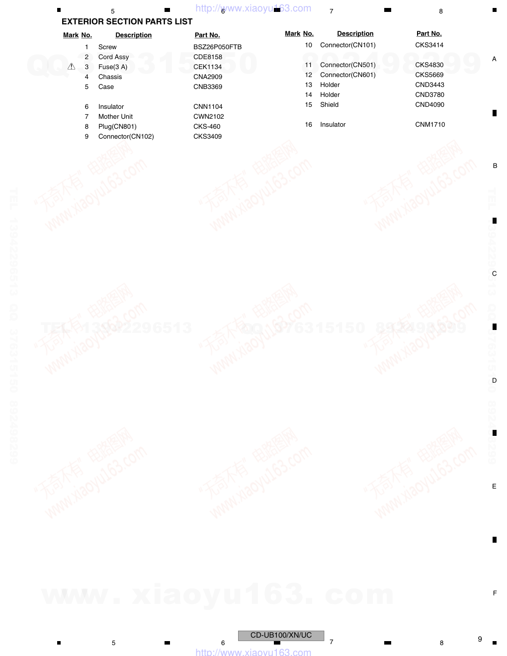
ORDER NO. PIONEER CORPORATION 4-1, Meguro 1-chome, Meguro-ku, Tokyo 153-8654, Japan PIONEER ELECTRONICS (USA) INC. P.O. Box 1760, Long Beach, CA 90801-1760, U.S.A. PIONEER EUROPE NV Haven 1087, Keetberglaan 1, 9120 Melsele, Belgium PIONEER ELECTRONICS ASIACENTRE PTE. LTD. 253 Alexandra Road, #04-01, Singapore 159936 PIONEER CORPORATION 2006 CD-UB100/XN/UC CRT3844 USB ADAPTER CD-UB100/XN/UC CD-UB100/XN/E5 For details, refer to "Important Check Points for Good Servicing". K-ZZA. DEC. 2006 Printed in Japan www. xiaoyu163. com QQ 376315150 9 9 2 8 9 4 2 9 8 TEL 13942296513 9 9 2 8 9 4 2 9 8 0 5 1 5 1 3 6 7 3 Q Q TEL 13942296513 QQ 376315150 892498299 TEL 13942296513 QQ 376315150 892498299 http://www.xiaoyu163.com CD-UB100/XN/UC 2 1 2 3 4 1 2 3 4 C D F A B E SAFETY INFORMATION CAUTION This service manual is intended for qualified service technicians; it is not meant for the casual do-it-yourselfer. Qualified technicians have the necessary test equipment and tools, and have been trained to properly and safely repair complex products such as those covered by this manual. Improperly performed repairs can adversely affect the safety and reliability of the product and may void the warranty. If you are not qualified to perform the repair of this product properly and safely, you should not risk trying to do so and refer the repair to a qualified service technician. WARNING This product contains lead in solder and certain electrical parts contain chemicals which are known to the state of California to cause cancer, birth defects or other reproductive harm. Health & Safety Code Section 25249.6 - Proposition 65 - Service Precaution 1. You should conform to the regulations governing the product (safety, radio and noise, and other regulations), and should keep the safety during servicing by following the safety instructions described in this manual. 2. Be careful in handling ICs. Some ICs such as MOS type are so fragile that they can be damaged by electrostatic induction. www. xiaoyu163. com QQ 376315150 9 9 2 8 9 4 2 9 8 TEL 13942296513 9 9 2 8 9 4 2 9 8 0 5 1 5 1 3 6 7 3 Q Q TEL 13942296513 QQ 376315150 892498299 TEL 13942296513 QQ 376315150 892498299 http://www.xiaoyu163.com CD-UB100/XN/UC 3 5 6 7 8 5 6 7 8 C D F A B E [Important Check Points for Good Servicing] In this manual, procedures that must be performed during repairs are marked with the below symbol. Please be sure to confirm and follow these procedures. 1. Product safety Please conform to product regulations (such as safety and radiation regulations), and maintain a safe servicing environment by following the safety instructions described in this manual. 1 Use specified parts for repair. Use genuine parts. Be sure to use important parts for safety. 2 Do not perform modifications without proper instructions. Please follow the specified safety methods when modification(addition/change of parts) is required due to interferences such as radio/TV interference and foreign noise. 3 Make sure the soldering of repaired locations is properly performed. When you solder while repairing, please be sure that there are no cold solder and other debris. Soldering should be finished with the proper quantity. (Refer to the example) 4 Make sure the screws are tightly fastened. Please be sure that all screws are fastened, and that there are no loose screws. 5 Make sure each connectors are correctly inserted. Please be sure that all connectors are inserted, and that there are no imperfect insertion. 6 Make sure the wiring cables are set to their original state. Please replace the wiring and cables to the original state after repairs. In addition, be sure that there are no pinched wires, etc. 7 Make sure screws and soldering scraps do not remain inside the product. Please check that neither solder debris nor screws remain inside the product. 8 There should be no semi-broken wires, scratches, melting, etc. on the coating of the power cord. Damaged power cords may lead to fire accidents, so please be sure that there are no damages. If you find a damaged power cord, please exchange it with a suitable one. 9 There should be no spark traces or similar marks on the power plug. When spark traces or similar marks are found on the power supply plug, please check the connection and advise on secure connections and suitable usage. Please exchange the power cord if necessary. 0 Safe environment should be secured during servicing. When you perform repairs, please pay attention to static electricity, furniture, household articles, etc. in order to prevent injuries. Please pay attention to your surroundings and repair safely. 2. Adjustments To keep the original performance of the products, optimum adjustments and confirmation of characteristics within specification. Adjustments should be performed in accordance with the procedures/instructions described in this manual. 4. Cleaning For parts that require cleaning, such as optical pickups, tape deck heads, lenses and mirrors used in projection monitors, proper cleaning should be performed to restore their performances. 3. Lubricants, Glues, and Replacement parts Use grease and adhesives that are equal to the specified substance. Make sure the proper amount is applied. 5. Shipping mode and Shipping screws To protect products from damages or failures during transit, the shipping mode should be set or the shipping screws should be installed before shipment. Please be sure to follow this method especially if it is specified in this manual. www. xiaoyu163. com QQ 376315150 9 9 2 8 9 4 2 9 8 TEL 13942296513 9 9 2 8 9 4 2 9 8 0 5 1 5 1 3 6 7 3 Q Q TEL 13942296513 QQ 376315150 892498299 TEL 13942296513 QQ 376315150 892498299 http://www.xiaoyu163.com CD-UB100/XN/UC 4 1 2 3 4 1 2 3 4 C D F A B E CONTENTS SAFETY INFORMATION..................................................................................................................................... 2 1. SPECIFICATIONS ............................................................................................................................................ 5 2. EXPLODED VIEWS AND PARTS LIST ............................................................................................................ 6 2.1 PACKING ................................................................................................................................................... 6 2.2 EXTERIOR................................................................................................................................................. 8 3. BLOCK DIAGRAM AND SCHEMATIC DIAGRAM.......................................................................................... 10 3.1 BLOCK DIAGRAM ................................................................................................................................... 10 3.2 OVERALL CONNECTION DIAGRAM(GUIDE PAGE).............................................................................. 12 4. PCB CONNECTION DIAGRAM ..................................................................................................................... 18 4.1 MOTHER UNIT ........................................................................................................................................ 18 5. ELECTRICAL PARTS LIST ............................................................................................................................ 22 6. ADJUSTMENT ............................................................................................................................................... 25 6.1 TEST MODE ............................................................................................................................................ 25 7. GENERAL INFORMATION............................................................................................................................. 26 7.1 DIAGNOSIS ............................................................................................................................................. 26 7.1.1 DISASSEMBLY ..................................................................................................................................... 26 7.1.2 CONNECTOR FUNCTION DESCRIPTION.......................................................................................... 27 7.2 IC ............................................................................................................................................................. 28 7.3 OPERATIONAL FLOW CHART ............................................................................................................... 35 8. OPERATIONS ................................................................................................................................................ 36 www. xiaoyu163. com QQ 376315150 9 9 2 8 9 4 2 9 8 TEL 13942296513 9 9 2 8 9 4 2 9 8 0 5 1 5 1 3 6 7 3 Q Q TEL 13942296513 QQ 376315150 892498299 TEL 13942296513 QQ 376315150 892498299 http://www.xiaoyu163.com CD-UB100/XN/UC 5 5 6 7 8 5 6 7 8 C D F A B E 1. SPECIFICATIONS www. xiaoyu163. com QQ 376315150 9 9 2 8 9 4 2 9 8 TEL 13942296513 9 9 2 8 9 4 2 9 8 0 5 1 5 1 3 6 7 3 Q Q TEL 13942296513 QQ 376315150 892498299 TEL 13942296513 QQ 376315150 892498299 http://www.xiaoyu163.com CD-UB100/XN/UC 6 1 2 3 4 1 2 3 4 C D F A B E 2. EXPLODED VIEWS AND PARTS LIST 2.1 PACKING NOTES : • Parts marked by " * " are generally unavailable because they are not in our Master Spare Parts List. • The > mark found on some component parts indicates the importance of the safety factor of the part. Therefore, when replacing, be sure to use parts of identical designation. • Screw adjacent to mark on the product are used for disassembly. • For the applying amount of lubricants or glue, follow the instructions in this manual. (In the case of no amount instructions,apply as you think it appropriate.) " 11 4 5 6 7 8 1 3 2 9 10 www. xiaoyu163. com QQ 376315150 9 9 2 8 9 4 2 9 8 TEL 13942296513 9 9 2 8 9 4 2 9 8 0 5 1 5 1 3 6 7 3 Q Q TEL 13942296513 QQ 376315150 892498299 TEL 13942296513 QQ 376315150 892498299 http://www.xiaoyu163.com CD-UB100/XN/UC 7 5 6 7 8 5 6 7 8 C D F A B E PACKING SECTION PARTS LIST Owner's Manual Mark No. Description Part No. 1 Cord Assy CDE5880 2 Cord Assy CDE8158 3 Cord Assy CDP1026 * 4 Accessory Assy CEA7408 5 Polyethylene Bag CEG1160 6 Fastener CNM6888 7 Fastener CNM6889 8 Air Cushioned Bag CEG1007 9 Carton(UC) CHG6068 Carton(E5) CHG6067 10 Contain Box(UC) CHL6068 Contain Box(E5) CHL6067 11-1 Owner's Manual(UC) CRD4151 Owner's Manual(E5) CRD4149 11-2 Owner's Manual(E5) CRD4150 * 11-3 Warranty Card(UC) CRY1246 * Warranty Card(E5) CRY1157 Mark No. Description Part No. Part No. Language CRD4151 English, French, Spanish CRD4149 English, Spanish, German, French, Italian CRD4150 Dutch, Russian, Portuguese(B), Traditional Chinese, Arabic www. xiaoyu163. com QQ 376315150 9 9 2 8 9 4 2 9 8 TEL 13942296513 9 9 2 8 9 4 2 9 8 0 5 1 5 1 3 6 7 3 Q Q TEL 13942296513 QQ 376315150 892498299 TEL 13942296513 QQ 376315150 892498299 http://www.xiaoyu163.com CD-UB100/XN/UC 8 1 2 3 4 1 2 3 4 C D F A B E 2.2 EXTERIOR 3 2 1 1 1 1 5 13 11 9 10 8 7 14 12 6 4 A 16 15 www. xiaoyu163. com QQ 376315150 9 9 2 8 9 4 2 9 8 TEL 13942296513 9 9 2 8 9 4 2 9 8 0 5 1 5 1 3 6 7 3 Q Q TEL 13942296513 QQ 376315150 892498299 TEL 13942296513 QQ 376315150 892498299 http://www.xiaoyu163.com CD-UB100/XN/UC 9 5 6 7 8 5 6 7 8 C D F A B E EXTERIOR SECTION PARTS LIST Mark No. Description Part No. 1 Screw BSZ26P050FTB 2 Cord Assy CDE8158 > 3 Fuse(3 A) CEK1134 4 Chassis CNA2909 5 Case CNB3369 6 Insulator CNN1104 7 Mother Unit CWN2102 8 Plug(CN801) CKS-460 9 Connector(CN102) CKS3409 10 Connector(CN101) CKS3414 11 Connector(CN501) CKS4830 12 Connector(CN601) CKS5669 13 Holder CND3443 14 Holder CND3780 15 Shield CND4090 16 Insulator CNM1710 Mark No. Description Part No. www. xiaoyu163. com QQ 376315150 9 9 2 8 9 4 2 9 8 TEL 13942296513 9 9 2 8 9 4 2 9 8 0 5 1 5 1 3 6 7 3 Q Q TEL 13942296513 QQ 376315150 892498299 TEL 13942296513 QQ 376315150 892498299 http://www.xiaoyu163.com CD-UB100/XN/UC 10 1 2 3 4 1 2 3 4 C D F A B E 3. BLOCK DIAGRAM AND SCHEMATIC DIAGRAM 3.1 BLOCK DIAGRAM BUSL1 11 7 7 3 5 1 7 IC351 NJM4558MD 18 17 19 +IN2B -IN2B -IN2A IC251 NJM4558MD 7 6 11 AOUTL LRCK BICK MCLK SDTI SMUTE RSTN 2 4 1 3 6 5 IC201 AK4388VT 9 14 SW2 OUT2 IC403 BA3131FS 7,24,40,58, 74,91,110,1 USBHO_DN VDDI1-6,VDDIO_3, VDDPLL,VDDPLL1 GPIO_D18 USBHO_DP GPIO_D19 GPIO_A1 nOE LRCK BCLK MCLK DA0 SFRM1 SCK1 SEL MUTE XA20 nCS3/nOE3 SD_nCS 79 80 95 96 49 53 47 48 nWE S S S 44 46 SD_CLK SD_CKE EXINT3 WUP 86 87 88 89 111 112 43 25 123 TC7 2 4 INA OUT 5 TC7S 3 USBTX USBRX 34 33 SYSPW USBPW 49 38 CN101 CN102 Q102 22 73 106 SYNC /BSENS Q401 Q402 MUTE ASENS 8 1 5 BUSL2 BUS- BUS+ DIN1 DIN2 5 6 1 2 27 19 72 28 42 79 29 STBY 8 IC101 HA12241FP 8 5 1 30 31 32 7 10 10 4 3 2 9 8 CN501 IP-OUT IP-IN IC505 S-80835CNNB-B8U RESET 1 VDD Q401 Q402 5V REGULATOR VDD BUP 67 /ASENB IPOUT(Tx) IPIN(Rx1) NC IPPW IPFLASHTX IPFLASHRX TESTCK BUSY /RESET NC35 CNVss 5 7 ASENB BUS+ BUS- BUSL3 ASENB BUS- BUS+ FLTX FLRX FLCLK FLBUSY FLCNVSS RSTSW VDD DALMON GND NC21 NC22 47 48 IC601 TCC8600-00X-EA-AG IC501 PEG297A CONTROL S501 (RESET) Xin Xout 15 13 11 2 1 nRESET XRST 24 77 XOUT XIN 54 X601 12MHz 55 MOTHER UNIT A www. xiaoyu163. com QQ 376315150 9 9 2 8 9 4 2 9 8 TEL 13942296513 9 9 2 8 9 4 2 9 8 0 5 1 5 1 3 6 7 3 Q Q TEL 13942296513 QQ 376315150 892498299 TEL 13942296513 QQ 376315150 892498299 http://www.xiaoyu163.com CD-UB100/XN/UC 11 5 6 7 8 5 6 7 8 C D F A B E 7,24,40,58,73, 74,91,110,124 IC841 NJM2872BF18 5 1 D3.3V IC851 NJM2885DL1-33 1 4 1 3 5 USBHO_DN -6,VDDIO_3, LL,VDDPLL1 GPIO_D18 USBHO_DP GPIO_D19 GPIO_A1 nOE XD8-XD15 XA0-XA19 XA20,XA21 nCS3/nOE3 SD_nCS /OE /CE /CS 79 80 95 96 49 53 47 48 11 16 /WE XXD0-XXD7 /WE WE nWE 28 26 19 OE FLCS SDCS XA0-XA16 XD0-XD15 38 37 CLK CKE SDCLK SDCKE 44 46 SD_CLK SD_CKE IC603 PEH083A FLASH ROM IC604 HY57V641620ETP-H SDRAM IC502 TC7SH08FUS1 2 4 4 2 INA OUTY OUTY INA ← 5V 3V IC503 TC7SET08FUS1 ← 3V 5V USBTX USBRX 34 33 SYSPW USBPW 49 38 IC831 NJM2872BF05 5 1,3 A8V Q811 Q812 DAC5V BUP 8V REGULATOR 5V REGULATOR 2 1 1 3 CN801 BUP CN601 VIN EN FLG VOUT USB5V 3 GND Shield 4 5 6 D- D+ 15 2 12 10 14 SW FB BIAS SYNC SHDN IC901 LT1766EFE-5 BUP Q861 BACKUP SENSE 22 73 Q601 106 SYNC /BSENS IC602 R5523N001B NC21 NC22 47 48 USBCTL FLG USBTX1 USBRX1 3 3.3V REGULATOR 1.8V REGULATOR 1 X-EA-AG 7A ROL Xin Xout X501 15.000MHz 13 11 ET T www. xiaoyu163. com QQ 376315150 9 9 2 8 9 4 2 9 8 TEL 13942296513 9 9 2 8 9 4 2 9 8 0 5 1 5 1 3 6 7 3 Q Q TEL 13942296513 QQ 376315150 892498299 TEL 13942296513 QQ 376315150 892498299 http://www.xiaoyu163.com CD-UB100/XN/UC 12 1 2 3 4 1 2 3 4 C D F A B E 3.2 OVERALL CONNECTION DIAGRAM(GUIDE PAGE) A-a A A-a A-a A-b A-b A-a A-a A-b A-b A-b A-b A-a A-a Large size SCH diagram Guide page Detailed page Note: When ordering service parts, be sure to refer to " EXPLODED VIEWS AND PARTS LIST" or "ELECTRICAL PARTS LIST". C953 470P C952 R001 L610 120 180 220 220 0R0 R632 47K www. xiaoyu163. com QQ 376315150 9 9 2 8 9 4 2 9 8 TEL 13942296513 9 9 2 8 9 4 2 9 8 0 5 1 5 1 3 6 7 3 Q Q TEL 13942296513 QQ 376315150 892498299 TEL 13942296513 QQ 376315150 892498299 http://www.xiaoyu163.com CD-UB100/XN/UC 13 5 6 7 8 5 6 7 8 C D F A B E A-b A 1.8 mH C953 470P 952 R001 Decimal points for resistor and capacitor fixed values are expressed as : 2.2 t 2R2 0.022 t R022 Symbol indicates a resistor. No differentiation is made between chip resistors and discrete resistors. NOTE : Symbol indicates a capacitor. No differentiation is made between chip capacitors and discrete capacitors. A MOTHER UNIT www. xiaoyu163. com QQ 376315150 9 9 2 8 9 4 2 9 8 TEL 13942296513 9 9 2 8 9 4 2 9 8 0 5 1 5 1 3 6 7 3 Q Q TEL 13942296513 QQ 376315150 892498299 TEL 13942296513 QQ 376315150 892498299 http://www.xiaoyu163.com CD-UB100/XN/UC 14 1 2 3 4 1 2 3 4 C D F A B E A-a A-b A-b 1 1.8 mH A MOTHER UNIT www. xiaoyu163. com QQ 376315150 9 9 2 8 9 4 2 9 8 TEL 13942296513 9 9 2 8 9 4 2 9 8 0 5 1 5 1 3 6 7 3 Q Q TEL 13942296513 QQ 376315150 892498299 TEL 13942296513 QQ 376315150 892498299 http://www.xiaoyu163.com CD-UB100/XN/UC 15 5 6 7 8 5 6 7 8 C D F A B E A-a A-b A-b Decimal points for resistor and capacitor fixed values are expressed as : 2.2 t 2R2 0.022 t R022 Symbol indicates a resistor. No differentiation is made between chip resistors and discrete resistors. NOTE : Symbol indicates a capacitor. No differentiation is made between chip capacitors and discrete capacitors. www. xiaoyu163. com QQ 376315150 9 9 2 8 9 4 2 9 8 TEL 13942296513 9 9 2 8 9 4 2 9 8 0 5 1 5 1 3 6 7 3 Q Q TEL 13942296513 QQ 376315150 892498299 TEL 13942296513 QQ 376315150 892498299 http://www.xiaoyu163.com CD-UB100/XN/UC 16 1 2 3 4 1 2 3 4 C D F A B E A-b A-a A-a A-b 1 C953 470P C952 R001 L610 120 180 220 www. xiaoyu163. com QQ 376315150 9 9 2 8 9 4 2 9 8 TEL 13942296513 9 9 2 8 9 4 2 9 8 0 5 1 5 1 3 6 7 3 Q Q TEL 13942296513 QQ 376315150 892498299 TEL 13942296513 QQ 376315150 892498299 http://www.xiaoyu163.com CD-UB100/XN/UC 17 5 6 7 8 5 6 7 8 C D F A B E A-a A-b A-b A-a 220 0R0 R632 47K www. xiaoyu163. com QQ 376315150 9 9 2 8 9 4 2 9 8 TEL 13942296513 9 9 2 8 9 4 2 9 8 0 5 1 5 1 3 6 7 3 Q Q TEL 13942296513 QQ 376315150 892498299 TEL 13942296513 QQ 376315150 892498299 http://www.xiaoyu163.com CD-UB100/XN/UC 18 1 2 3 4 1 2 3 4 C D F A B E 4. PCB CONNECTION DIAGRAM 4.1 MOTHER UNIT A A MOTHER UNIT NOTE FOR PCB DIAGRAMS 1.The parts mounted on this PCB include all necessary parts for several destination. For further information for respective destinations, be sure to check with the schematic dia- gram. Capacitor Connector P.C.Board Chip Part SIDE B SIDE A 2.Viewpoint of PCB diagrams 10 20 30 40 50 60 70 10 20 30 40 50 60 70 80 0 X Y FRONT IP-BUS OUT RESET USB IP-BUS IN www. xiaoyu163. com QQ 376315150 9 9 2 8 9 4 2 9 8 TEL 13942296513 9 9 2 8 9 4 2 9 8 0 5 1 5 1 3 6 7 3 Q Q TEL 13942296513 QQ 376315150 892498299 TEL 13942296513 QQ 376315150 892498299 http://www.xiaoyu163.com CD-UB100/XN/UC 19 5 6 7 8 5 6 7 8 C D F A B E A SIDE A 70 80 90 100 110 120 130 140 FRONT IN POWER SUPPLY www. xiaoyu163. com QQ 376315150 9 9 2 8 9 4 2 9 8 TEL 13942296513 9 9 2 8 9 4 2 9 8 0 5 1 5 1 3 6 7 3 Q Q TEL 13942296513 QQ 376315150 892498299 TEL 13942296513 QQ 376315150 892498299 http://www.xiaoyu163.com CD-UB100/XN/UC 20 1 2 3 4 1 2 3 4 C D F A B E A A MOTHER UNIT 70 80 90 100 110 120 130 140 R632 L61 www. xiaoyu163. com QQ 376315150 9 9 2 8 9 4 2 9 8 TEL 13942296513 9 9 2 8 9 4 2 9 8 0 5 1 5 1 3 6 7 3 Q Q TEL 13942296513 QQ 376315150 892498299 TEL 13942296513 QQ 376315150 892498299 http://www.xiaoyu163.com CD-UB100/XN/UC 21 5 6 7 8 5 6 7 8 C D F A B E A SIDE B 10 20 30 40 50 60 70 10 20 30 40 50 60 70 80 0 X Y L610 www. xiaoyu163. com QQ 376315150 9 9 2 8 9 4 2 9 8 TEL 13942296513 9 9 2 8 9 4 2 9 8 0 5 1 5 1 3 6 7 3 Q Q TEL 13942296513 QQ 376315150 892498299 TEL 13942296513 QQ 376315150 892498299 http://www.xiaoyu163.com CD-UB100/XN/UC 22 1 2 3 4 1 2 3 4 C D F A B E 5. ELECTRICAL PARTS LIST NOTE: • Parts whose parts numbers are omitted are subject to being not supplied. • The part numbers shown below indicate chip components. Chip Resistor RS1/_S___J,RS1/__S___J Chip Capacitor (except for CQS.....) CKS....., CCS....., CSZS..... • The > mark found on some component parts indicates the importance of the safety factor of the part. Therefore, when replacing, be sure to use parts of identical designation. • Meaning of the figures and others in the parentheses in the parts list. Example) IC 301 is on the point (face A, 91 of x-axis, and 111 of y-axis) of the corresponding PC board. IC 301 (A, 91, 111) IC NJM2068V Circuit Symbol and No. Part No. A Unit Number: CWN2102 Unit Name : Mother Unit MISCELLANEOUS IC 101 (A,25,78) IC HA12241FP IC 201 (A,37,27) IC AK4388VT IC 251 (A,35,57) IC NJM4558MD IC 351 (A,81,68) IC NJM4558MD IC 352 (A,81,77) IC NJM4558MD IC 403 (A,54,61) IC BA3131FS IC 501 (A,17,30) IC PEG297A IC 502 (A,32,11) IC TC7SH08FUS1 IC 503 (A,32,16) L-MOS TC7SET08FUS1 IC 505 (A,23,9) IC S-80835CNNB-B8U IC 601 (A,61,29) USB Media Control IC TCC8600-00X-EA-AG IC 602 (A,81,6) IC R5523N001B IC 603 (A,108,36) IC PEH083A IC 604 (A,109,18) SD-RAM(64M) HY57V641620ETP-H IC 831 (A,45,50) IC NJM2872BF05 IC 841 (A,116,45) IC NJM2872BF18 IC 851 (A,134,36) IC NJM2885DL1-33 IC 901 (A,124,57) IC LT1766EFE-5 Q 102 (B,57,69) Transistor 2SC4081 Q 401 (A,40,66) Transistor UMX1N Q 402 (A,91,58) Transistor UMF23N Q 601 (A,66,11) Chip Transistor DTC114EWA Q 811 (A,97,61) Transistor 2SD1767 Q 812 (A,105,63) Transistor UMD2N Q 821 (B,115,54) Transistor 2SD1767 Q 822 (A,116,53) Transistor UMD2N Q 861 (A,90,63) Transistor 2SC4081 D 501 (A,24,6) Diode MA111 D 601 (B,51,11) Diode MALS068X D 602 (B,49,11) Diode MALS068X D 801 (A,122,79) Diode MPG06G-6415G50 D 811 (A,102,61) Diode HZS9L(B3) D 812 (A,23,42) Diode DAN202U D 821 (A,115,50) Diode HZS6L(B1) D 822 (A,112,68) Diode MPG06G-6415G50 D 861 (A,97,67) Diode HZS7L(C3) D 901 (A,128,63) Diode RB160L-40 D 902 (A,129,55) Diode 1SS355 D 903 (A,112,72) Diode MPG06G-6415G50 L 101 (A,26,70) Inductor LCTC3R3K2125 L 202 (A,42,33) Inductor CTF1379 L 501 (A,17,45) Ferri-Inductor LAU100K L 502 (A,34,13) Inductor CTF1379 L 503 (A,33,18) Inductor CTF1379 L 601 (A,68,46) Inductor CTF1379 L 602 (A,74,46) Inductor CTF1379 L 603 (A,48,42) Inductor CTF1379 L 606 (B,99,32) Inductor CTF1379 L 607 (A,92,20) Inductor CTF1379 L 608 (A,46,36) Inductor LCTC2R2K1608 L 609 (A,46,32) Inductor LCTC2R2K1608 L 610 (B,71,19) Inductor CTF1384 L 801 (A,134,76) Choke Coil 1.8 mH CTH1367 L 901 (A,135,58) Inductor CTH1255 X 501 (A,16,15) Crystal Resonator 15.000 MHz CSS1653 X 601 (A,58,43) Crystal Resonator 12.000 MHz CSS1723 S 501 (A,14,4) Switch(RESET) CSG1046 RESISTORS R 101 (A,28,69) RS1/16S102J R 102 (A,24,71) RS1/16S101J R 103 (A,23,71) RS1/16S101J R 104 (B,57,76) RS1/16S473J R 105 (B,57,73) RS1/16S223J R 106 (A,31,68) RS1/16S472J R 107 (A,31,67) RS1/16S472J R 201 (A,42,23) RS1/16S101J R 202 (A,42,21) RS1/16S101J R 203 (B,46,30) RS1/16S473J R 204 (B,44,30) RS1/16S473J R 205 (B,48,30) RS1/16S473J R 206 (A,42,30) RS1/16S473J R 251 (A,31,53) RS1/16S103J R 252 (A,40,53) RS1/16S103J Circuit Symbol and No. Part No. www. xiaoyu163. com QQ 376315150 9 9 2 8 9 4 2 9 8 TEL 13942296513 9 9 2 8 9 4 2 9 8 0 5 1 5 1 3 6 7 3 Q Q TEL 13942296513 QQ 376315150 892498299 TEL 13942296513 QQ 376315150 892498299 http://www.xiaoyu163.com CD-UB100/XN/UC 23 5 6 7 8 5 6 7 8 C D F A B E R 253 (B,33,57) RS1/16S103J R 254 (B,38,57) RS1/16S103J R 255 (B,33,55) RS1/16S103J R 256 (B,38,55) RS1/16S103J R 257 (B,33,62) RS1/16S153J R 258 (B,37,62) RS1/16S153J R 259 (A,34,53) RS1/16S151J R 260 (A,37,53) RS1/16S151J R 301 (A,44,54) RS1/16S103J R 302 (A,43,53) RS1/16S103J R 303 (B,50,65) RS1/16S473J R 304 (B,50,61) RS1/16S473J R 305 (A,51,67) RS1/16S103J R 306 (A,51,54) RS1/16S103J R 307 (B,52,65) RS1/16S153J R 308 (B,52,61) RS1/16S153J R 309 (A,55,67) RS1/16S153J R 310 (A,54,55) RS1/16S153J R 311 (B,54,65) RS1/16S473J R 312 (B,54,61) RS1/16S473J R 313 (A,68,64) RS1/16S133J R 314 (A,71,58) RS1/16S133J R 315 (A,68,63) RS1/16S133J R 316 (A,68,60) RS1/16S133J R 317 (B,24,42) RS1/16S153J R 351 (A,71,64) RS1/16S361J R 352 (A,72,58) RS1/16S361J R 353 (A,71,63) RS1/16S361J R 354 (A,71,60) RS1/16S361J R 355 (A,74,71) RS1/16S104J R 356 (A,74,74) RS1/16S104J R 357 (A,74,65) RS1/16S104J R 358 (A,74,80) RS1/16S104J R 359 (A,74,66) RS1/16S102J R 360 (A,74,79) RS1/16S102J R 361 (A,74,68) RS1/16S223J R 362 (A,74,77) RS1/16S223J R 363 (A,74,69) RS1/16S181J R 364 (A,74,76) RS1/16S181J R 401 (A,42,66) RS1/16S102J R 402 (A,38,64) RS1/16S102J R 403 (B,42,79) RS1/16S223J R 404 (B,39,73) RS1/16S223J R 405 (A,92,61) RS1/16S332J R 406 (A,89,60) RS1/16S562J R 407 (B,40,65) RS1/16S103J R 408 (B,42,65) RS1/16S103J R 501 (B,14,21) RS1/16S473J R 502 (B,12,19) RS1/16S0R0J R 503 (B,17,21) RS1/16S473J R 504 (B,7,34) RS1/16S473J R 505 (B,11,36) RS1/16S473J R 506 (B,22,47) RS1/16S473J R 507 (B,19,21) RS1/16S104J R 508 (B,22,63) RS1/16S473J R 509 (B,8,46) RS1/16S473J R 510 (B,9,34) RS1/16S473J R 511 (B,13,30) RS1/16S473J R 512 (A,20,10) RS1/16S102J R 513 (A,21,7) RS1/16S183J Circuit Symbol and No. Part No. R 514 (A,34,10) RS1/16S101J R 515 (A,32,14) RS1/16S101J R 517 (A,14,51) RS1/16S104J R 519 (B,24,33) RS1/16S473J R 520 (B,28,33) RS1/16S473J R 521 (B,23,21) RS1/16S272J R 522 (B,25,21) RS1/16S472J R 523 (B,26,33) RS1/16S473J R 524 (B,23,38) RS1/16S104J R 525 (B,25,28) RS1/16S473J R 528 (B,26,24) RS1/16S272J R 529 (B,25,26) RS1/16S472J R 530 (B,21,21) RS1/16S222J R 532 (B,9,49) RS1/16S104J R 601 (A,69,11) RS1/16S472J R 602 (A,48,30) RS1/16S473J R 603 (B,48,26) RS1/16S270J R 604 (B,50,26) RS1/16S270J R 605 (A,43,26) RAB4CQ101J R 606 (B,63,21) RS1/16S473J R 607 (A,49,26) RS1/16S221J R 608 (A,50,39) RS1/16S473J R 609 (B,41,21) RS1/16S101J R 610 (B,40,19) RS1/16S101J R 611 (B,69,27) RS1/16S473J R 612 (A,74,17) RAB4CQ101J R 613 (A,74,20) RAB4CQ101J R 614 (A,75,23) RAB4CQ101J R 615 (A,75,26) RAB4CQ101J R 616 (A,75,29) RAB4CQ101J R 617 (A,75,32) RAB4CQ101J R 618 (A,75,35) RAB4CQ101J R 619 (A,81,37) RAB4CQ221J R 620 (A,81,40) RAB4CQ221J R 621 (B,72,17) RS1/16S181J R 622 (B,73,15) RS1/16S101J R 624 (A,64,44) RS1/16S473J R 625 (A,59,39) RS1/16SS102J R 626 (A,59,40) RS1/16SS205J R 627 (B,73,13) RS1/16S101J R 628 (B,73,11) RS1/16S271J R 629 (B,50,5) RS1/16S0R0J R 630 (B,69,8) RS1/16S0R0J R 631 (B,75,20) RS1/16S121J R 632 (B,113,23) RS1/16S473J R 633 (B,47,11) RS1/16S153J R 634 (B,53,11) RS1/16S153J R 636 (B,52,28) RS1/16S473J R 639 (A,99,25) RS1/16SS0R0J R 656 (A,100,25) RS1/16SS101J R 657 (A,101,25) RS1/16SS101J R 658 (A,103,25) RS1/16SS101J R 659 (A,104,25) RS1/16SS101J R 660 (A,105,25) RS1/16SS101J R 661 (A,106,25) RS1/16SS101J R 662 (A,108,25) RS1/16SS101J R 663 (A,97,12) RS1/16SS0R0J R 664 (A,100,10) RS1/16SS101J R 665 (A,101,10) RS1/16SS101J R 666 (A,103,10) RS1/16SS101J R 667 (A,104,10) RS1/16SS101J Circuit Symbol and No. Part No. www. xiaoyu163. com QQ 376315150 9 9 2 8 9 4 2 9 8 TEL 13942296513 9 9 2 8 9 4 2 9 8 0 5 1 5 1 3 6 7 3 Q Q TEL 13942296513 QQ 376315150 892498299 TEL 13942296513 QQ 376315150 892498299 http://www.xiaoyu163.com CD-UB100/XN/UC 24 1 2 3 4 1 2 3 4 C D F A B E R 668 (A,105,10) RS1/16SS101J R 669 (A,106,10) RS1/16SS101J R 670 (A,108,10) RS1/16SS0R0J R 672 (B,88,25) RS1/16S0R0J R 811 (A,108,63) RS1/16S182J R 821 (B,119,55) RS1/16S333J R 822 (A,118,53) RS1/16S822J R 823 (B,118,66) RS1/16S360J R 824 (B,118,64) RS1/16S360J R 861 (A,92,65) RS1/16S104J R 862 (A,91,67) RS1/16S473J R 901 (A,126,51) RS1/16S0R0J R 903 (A,124,50) RS1/16S332J CAPACITORS C 101 (B,60,73) CKSRYB104K16 C 102 (B,25,76) CKSRYB104K16 C 103 (B,23,76) CKSRYB102K50 C 104 (B,21,76) CKSRYB102K50 C 204 (A,39,34) CKSYB106K6R3 C 205 (A,41,33) CKSRYB102K50 C 206 (A,42,35) CKSRYB102K50 C 207 (A,37,34) CKSYB106K6R3 C 208 (A,35,32) CKSRYB104K16 C 251 (A,31,49) CEJQ100M16 C 252 (A,36,49) CEJQ100M16 C 253 (B,31,61) CCSRCH681J50 C 254 (B,39,61) CCSRCH681J50 C 255 (B,31,56) CCSRCH181J50 C 256 (B,40,56) CCSRCH181J50 C 257 (A,27,54) CEAT220M25 C 259 (B,24,55) CKSRYB104K16 C 301 (A,63,56) CEAT470M10 C 302 (B,59,64) CKSRYB103K50 C 303 (A,53,72) CEAT220M25 C 304 (A,63,64) CEAT101M16 C 351 (A,85,68) CKSRYB104K16 C 352 (A,85,77) CKSRYB104K16 C 353 (A,77,66) CKSRYB105K10 C 354 (A,77,79) CKSRYB105K10 C 355 (A,77,69) CKSRYB105K10 C 356 (A,77,76) CKSRYB105K10 C 401 (A,46,65) CEJQ100M16 C 402 (A,46,59) CEJQ100M16 C 501 (A,10,44) CEAT4R7M50 C 502 (B,12,44) CKSRYB103K50 C 504 (B,17,12) CCSRCH180J50 C 505 (B,13,12) CCSRCH180J50 C 507 (A,25,9) CKSRYB105K10 C 508 (A,29,11) CKSRYB104K16 C 509 (A,29,16) CKSRYB104K16 C 601 (B,68,40) CKSRYB104K16 C 602 (A,68,42) CEJQ100M16 C 603 (B,74,41) CKSRYB104K16 C 604 (A,74,42) CEJQ100M16 C 605 (A,48,38) CKSYB475K10 C 606 (A,50,36) CKSRYB104K16 C 607 (A,49,34) CKSRYB122K50 C 608 (A,49,32) CKSRYB331K50 Circuit Symbol and No. Part No. C 609 (B,54,28) CKSRYB104K16 C 610 (B,55,21) CKSRYB104K16 C 611 (A,45,34) CKSRYB103K50 C 612 (B,66,21) CKSRYB104K16 C 614 (B,71,21) CKSRYB104K16 C 615 (B,69,25) CKSRYB104K16 C 616 (B,71,31) CKSRYB104K16 C 617 (B,71,35) CKSRYB104K16 C 618 (B,66,36) CKSRYB104K16 C 619 (A,57,41) CCSSCH5R0C50 C 620 (A,60,41) CCSSCH150J50 C 621 (B,61,33) CKSRYB104K16 C 624 (A,84,10) CKSRYB104K16 C 625 (B,87,6) CKSRYB104K16 C 626 (A,90,6) CEJQ100M16 C 627 (B,102,29) CKSRYB104K16 C 628 (B,102,33) CKSRYB104K16 C 629 (B,98,16) CKSRYB104K16 C 630 (B,100,16) CKSRYB104K16 C 631 (B,105,16) CKSRYB104K16 C 632 (B,109,16) CKSRYB104K16 C 633 (B,119,16) CKSRYB104K16 C 634 (B,102,19) CKSRYB104K16 C 635 (B,107,19) CKSRYB104K16 C 801 (A,112,79) CEAT102M16 C 802 (B,112,75) CKSRYB104K16 C 803 (B,91,78) CKSRYB103K50 C 811 (B,99,56) CKSRYB104K16 C 812 (A,99,54) CEAT470M10 C 813 (B,106,60) CKSRYB104K16 C 814 (A,106,58) CEJQ100M16 C 821 (B,111,52) CKSRYB103K50 C 822 (A,108,52) CEAT470M10 C 823 (A,113,53) CKSRYB103K50 C 824 (A,115,60) CEAT102M16 C 831 (A,48,49) CKSRYB102K50 C 833 (A,44,45) CEJQ100M16 C 834 (A,43,49) CKSRYB104K16 C 841 (A,112,45) CKSYB475K10 C 842 (A,116,47) CKSRYB104K16 C 843 (A,122,44) CKSYB475K10 C 844 (A,120,45) CKSRYB104K16 C 851 (B,129,40) CKSRYB103K50 C 852 (A,127,40) CEAT101M16 C 853 (B,136,41) CKSYB475K10 C 854 (A,135,43) CKSRYB104K16 C 901 (A,131,47) CEHAZL101M25 C 902 (A,129,58) CKSRYB334K10 C 903 (A,124,62) CKSRYB104K16 C 904 (A,124,65) 4.7 µF CCG1111 C 905 (A,122,50) CKSRYB472K50 C 906 (A,121,72) CEAT471M16 C 907 (A,124,49) CKSRYB473K50 C 908 (B,54,35) CKSQYB106K6R3 C 952 (B,132,8) CCSRCH102J50 C 953 (B,121,23) CCSRCH471J50 Circuit Symbol and No. Part No. www. xiaoyu163. com QQ 376315150 9 9 2 8 9 4 2 9 8 TEL 13942296513 9 9 2 8 9 4 2 9 8 0 5 1 5 1 3 6 7 3 Q Q TEL 13942296513 QQ 376315150 892498299 TEL 13942296513 QQ 376315150 892498299 http://www.xiaoyu163.com CD-UB100/XN/UC 25 5 6 7 8 5 6 7 8 C D F A B E 6. ADJUSTMENT 6.1 TEST MODE V e r * . * * V e r * . * * U P D T 0 0 0 R E A D Y 0 0 0 MIN SEC SEC C O M P L E T E D e v i c e I n C o n n e c t M S C Normal connection Indication of TCC firmware Ver In the test mode Indication of system microcomputer Ver TCC firmware VerUp is started. Activate the test mode * Refer to the service manual of connected head unit regarding how to activate the test mode. Enter the TEST1 command TCC firmware VerUp is completed. Indication of connection mode Enter the TEST3 command Passage of time : For about several tens of seconds Enter the TEST4 command Insert a USB device for confirmation Enter the TEST2 command TCC firmware VerUp is getting ready. Indication of connection mode is getting ready. Insert a USB device for updating Reset start Now connecting Passage of time : For about several tens of seconds Enter the TEST0 command Enter the TEST0 command Enter the TEST0 command - Implemented functions • Indication of system microcomputer Ver • Indication of TCC firmware Ver • To enter the TCC firmware UpDate mode: →Set this mode and insert a USB device having the UpDate program to start rewriting the device. * If you carry out the TEST 3 command with the USB device inserted, a correct result is not displayed. • Confirmation on connection mode (mass storage class connection) →Set this mode and insert a USB device. Then, the connection mode is displayed. * Do not insert a USB device having the UpDate program. * If you carry out the TEST 4 command with the USB device inserted, a correct result is not displayed. Be sure to insert a USB device when "DeviceIn" is being displayed. Indication of system microcomputer Ver Indication of TCC firmware Ver TCC firmware VerUp is getting ready. TCC firmware VerUp is started. TCC firmware VerUp is completed. Confirmation on connection mode is getting ready. Now connecting Indication of connection mode When a device supporting mass storage class is connected Displays 0:00 to 5:00 (in increments of minutes and seconds) Displays 0:00 to 5:00 (in increments of minutes and seconds) * The time increment stops when it reaches 5:00. - Indications Model with 1-6 keys Main unit Main unit (only the model 07) Remote control TEST1 command TEST2 command TEST3 command TEST4 command TEST0 command Right key Left key Key 1 Key 2 BAND/ESC key Model without 1-6 keys Right key Left key LIST key DISP key BAND/ESC key Right key Left key Key 1 Key 2 BAND/ESC key www. xiaoyu163. com QQ 376315150 9 9 2 8 9 4 2 9 8 TEL 13942296513 9 9 2 8 9 4 2 9 8 0 5 1 5 1 3 6 7 3 Q Q TEL 13942296513 QQ 376315150 892498299 TEL 13942296513 QQ 376315150 892498299 http://www.xiaoyu163.com CD-UB100/XN/UC 26 1 2 3 4 1 2 3 4 C D F A B E 7. GENERAL INFORMATION 7.1 DIAGNOSIS 7.1.1 DISASSEMBLY 1 Fig.1 - Removing the Case (Fig.1) Case Fig.2 Mother Unit - Removing the Mother Unit (Fig.2) Straighten the tabs at three locations indicated. Remove the Mother Unit. 1 Remove the four screws and then remove the Case. 1 1 1 1 1 1 1 www. xiaoyu163. com QQ 376315150 9 9 2 8 9 4 2 9 8 TEL 13942296513 9 9 2 8 9 4 2 9 8 0 5 1 5 1 3 6 7 3 Q Q TEL 13942296513 QQ 376315150 892498299 TEL 13942296513 QQ 376315150 892498299 http://www.xiaoyu163.com CD-UB100/XN/UC 27 5 6 7 8 5 6 7 8 C D F A B E 7.1.2 CONNECTOR FUNCTION DESCRIPTION POWER SUPPLY IP-BUS IN(BLUE) IP-BUS OUT(BLACK) 1 2 3 1 2 6 7 8 9 10 11 3 4 5 BUSL2 BUSR2 BUSR1 ASENB BUSL1 BUSG1 BUS - NC BUSG1 BUSG1 BUS + BUS + BUSG5 BUSG5 NC BUS - BUSG5 BUSL3 ASENB BUSR3 BUSAG1 BUSAG1 1 2 6 7 8 9 10 11 3 4 5 1 2 3 4 5 6 7 8 9 10 11 1 2 3 5 6 7 8 9 10 11 4 NC B. UP GND 1 2 3 USB USB5V D- D+ GND 1 2 3 4 1 2 3 4 www. xiaoyu163. com QQ 376315150 9 9 2 8 9 4 2 9 8 TEL 13942296513 9 9 2 8 9 4 2 9 8 0 5 1 5 1 3 6 7 3 Q Q TEL 13942296513 QQ 376315150 892498299 TEL 13942296513 QQ 376315150 892498299 http://www.xiaoyu163.com CD-UB100/XN/UC 28 1 2 3 4 1 2 3 4 C D F A B E 7.2 IC - Pin Functions(PEG297A) Pin No. Pin Name I/O Function and Operation 1-5 6 7 8,9 10 11 12 13 14 15 16-18 19 20,21 22 23 24 25 26 27 28 29 30 31 32 33 34 35-37 38 39 40,41 42 43 44 45,46 47 48 49 50-53 54 55 56 57,58 59 60 61 62 63-66 67 68-70 71 72 73 74 75 76-78 NC BYTE CNVSS NC RESET XOUT VSS XIN VCC nmi NC RX2 NC DDSYNC NC xrst WUP NC RX TX TXD RXD/TSI SCLK/TSLK BUSY USBTX USBRX NC USBPW EPM NC MUTE SEL CE NC USBCTL flg SYSPW NC USBTEST_TRK USBTEST_NOW USBTEST_NG NC USBTEST_IN VDD NC VSS NC DALMON NC ROMCS asensb bsens ROMCK ROMDATA NC I I O O O O O I O O I O I O I O O I O O I I O I/O Not used External data bus width change input Processor mode change input Not used Reset input Clock output Power supply input Clock input Power supply input NMI input Not used IPBUS : Input 2 Not used DD converter synchronous clock output Not used TCC860 reset output For TCC860WakeUp(uncontrolled) Not used IPBUS : Input IPBUS : Output For flash rewriting For flash rewriting(combined with communication terminal for chip check) For flash rewriting(combined with communication terminal for chip check) For flash rewriting For TCC860 communication For TCC860 communication Not used DD converter power supply control output For flash rewriting Not used MUTE output Selector output For flash rewriting Not used USB bus power control output Overcurrent detection output System power control output Not used TrackUP operation terminal TEST(SDRAM, Vendor ID check) completion determination terminal OK/NG output terminal Not used TESTIN terminal for USB Power supply input Not used Power supply input Not used For consumption current reduction output Not used ROM correction chip select output ASENBO sense Back up sense input ROM correction : Clock output ROM correction : Data input/output Not used www. xiaoyu163. com QQ 376315150 9 9 2 8 9 4 2 9 8 TEL 13942296513 9 9 2 8 9 4 2 9 8 0 5 1 5 1 3 6 7 3 Q Q TEL 13942296513 QQ 376315150 892498299 TEL 13942296513 QQ 376315150 892498299 http://www.xiaoyu163.com CD-UB100/XN/UC 29 5 6 7 8 5 6 7 8 C D F A B E - Pin Layout MCLK BICK SDTI LRCK RSTN SMUTE ACKS DIF0 DZF DEM VDD VSS VCOM AOUTL AOUTR DIF1 1 2 3 4 5 6 7 8 16 15 14 13 12 11 10 9 - Block Diagram DEM SMUTE ACKS DIF0 DIF1 LRCK BICK SDTI AOUTR AOUTL Control Port De-emphasis Control 8X Interpolator 8X Interpolator Clock Divider Audio Data Interface MCLK RSTN ΔΣ Modulator VDD VSS VCOM DZF ΔΣ Modulator SCF LPF SCF LPF AK4388VT PEG297A 50 76 100 26 75 1 25 51 Pin No. Pin Name I/O Function and Operation 79 80-85 86 87-93 94 95 96 97 98-100 IPPW NC TESTIN NC AVSS NC VREF AVCC NC O I IPBUS : Driver power supply control output Not used Test program input Not used A/D converter power supply input terminal Not used AD translation reference voltage A/D converter power supply input terminal Not used www. xiaoyu163. com QQ 376315150 9 9 2 8 9 4 2 9 8 TEL 13942296513 9 9 2 8 9 4 2 9 8 0 5 1 5 1 3 6 7 3 Q Q TEL 13942296513 QQ 376315150 892498299 TEL 13942296513 QQ 376315150 892498299 http://www.xiaoyu163.com CD-UB100/XN/UC 30 1 2 3 4 1 2 3 4 C D F A B E - Pin Functions(TCC8600-00X-EA-AG) Pin No. Pin Name I/O Function and Operation 1 2-6 7 8 9 10-16 17-23 24 25 26 27-39 40 41,42 43 44 45 46 47 48 49 50 51 52 53 54 55 56 57 58 59 60 61 62 63 64 65 66 67 68 69 70 71 72 73 74 75 76 77 78 79 80 81 82 83 84 VSS XD[4]-[8] VDDI VSS VDDIO XD[9]-[15] XA[0]-[6] VDDI VSS VDDIO XA[7]-[19] VDDI XA[20], [21] VDDIO SD_CLK VSS SD_CKE SD_nCS nWE nOE nCS[0]/ND_nOE[0] nCS[1]/ND_nOE[1] nCS[2]/ND_nOE[2] nCS[3]/ND_nOE[3] XOUT XIN XTOUT XTIN VDDI VSS GPIO_B[6] ND_nWE UART0TXD UART0RXD READY VDDIO ADIN4 ADIN2 ADIN0 VDDADC VSSADC VSSPLL1 XFILT1 VDDPLL1 VDDPLL XFILT VSSPLL nRESET MODE1 USBH0_DN USBH0_DP VSS USBH1_DN USBH1_DP VDDUSB I/O I/O I/O I/O I/O I/O I/O I/O I/O I/O I/O I/O I/O I/O O I O I I/O I/O I/O I/O I I I I/O I/O I/O I/O Digital ground External bus data bit [4]-[8]. Internal pull-up resistor enabled at reset. Digital power for internal core (1.8 V) Digital ground Digital power for I/O (3.3 V) External bus data bit [9]-[15]. Internal pull-up resistor enabled at reset. External bus address bit [0]-[6] Digital power for internal core (1.8 V) Digital ground Digital power for I/O (3.3 V) External bus address bit [7]-[19] Digital power for internal core (1.8 V) External bus address bit [20], [21] Digital power for I/O (3.3 V) SDRAM clock Digital ground SDRAM clock enable signal. Active high. Chip select signal for SDRAM, active low Static memory write enable signal. Active low. Static memory output enable signal. Active low. External bus chip select [0] / NAND flash output enable [0] External bus chip select [1] / NAND flash output enable [1] External bus chip select [2] / NAND flash output enable [2] External bus chip select [3] / NAND flash output enable [3] 12 MHz crystal oscillator output 12 MHz crystal oscillator input. Voltage must not exceed VDDI (1.95 V). 32.768 kHz crystal oscillator output 32.768 kHz crystal oscillator input. Voltage must not exceed VDDI (1.95 V). Digital power for internal core (1.8 V) Digital ground GPIO_B[6] NAND flash WE. Active low UART0 TX data UART0 RX data Ready information from external device. Digital power for I/O (3.3 V) General purpose multi-channel ADC input 4 General purpose multi-channel ADC input 2 General purpose multi-channel ADC input 0 Analog power for ADC (3.3 V) Analog ground for ADC Analog ground for PLL PLL1 filter output. 1 200 pF capacitor is required. Analog & digital power for PLL1 (1.8 V) Analog & digital power for PLL (1.8 V) PLL0 filter output. 350 pF capacitor is required. Analog ground for PLL System Reset. Active low. Mode setting input 1. Pull-down for normal operation. USB host port 0 D- signal USB host port 0 D+ signal Digital ground USB host port 1 D- signal USB host port 1 D+ signal Power for USB I/O (3.3 V) www. xiaoyu163. com QQ 376315150 9 9 2 8 9 4 2 9 8 TEL 13942296513 9 9 2 8 9 4 2 9 8 0 5 1 5 1 3 6 7 3 Q Q TEL 13942296513 QQ 376315150 892498299 TEL 13942296513 QQ 376315150 892498299 http://www.xiaoyu163.com CD-UB100/XN/UC 31 5 6 7 8 5 6 7 8 C D F A B E TCC8600-00X-EA-AG 128 33 64 97 32 65 96 1 Pin No. Pin Name I/O Function and Operation 85 86 87 88 89 90 91 92 93 94 95,96 97 98,99 100 101 102 103 104 105 106 107 108 109 110 111 112 113 114 115 116 117 118 119 120-123 124 125-128 VDDIO BCLK LRCK MCLK DAO DAI VDDI GPIO_D[15] GPIO_D[16] GPIO_D[17] GPIO_D[18],[19] VSS GPIO_D[20],[21] TDI TMS TCK TDO nTRST GPIO_A[0] GPIO_A[1 GPIO_A[2] GPIO_A[3] GPIO_A[4] VDDI GPIO_A[5] GPIO_A[6] GPIO_A[7] GPIO_A[8] GPIO_A[9] GPIO_A[10] GPIO_A[11] VSS VDDIO EXINT[0]-[3] VDDI XD[0]-[3] I/O I/O I/O I/O I/O I/O I/O I/O I/O I/O I/O I/O I/O I/O I/O I/O I/O I/O I/O I/O I/O I/O I/O I/O I/O I/O I/O I/O I/O Digital power for I/O (3.3 V) I2S bit clock / Boot mode bit 0 (BM[0]) I2S word clock / Boot mode bit 1 (BM[1]) I2S System Clock I2S digital audio data output / Boot mode bit 2 (BM[2]) I2S digital audio data input Digital power for internal core (1.8 V) GPIO_D[15] GPIO_D[16] / I2C SDA GPIO_D[17] / I2C SCL GPIO_D[18], [19]. Internal pull-up resistor enabled at reset. Digital ground GPIO_D[21], [20]. Internal pull-up resistor enabled at reset. JTAG serial data input. Internal pull-up resistor is enabled at reset JTAG test mode select. Internal pull-up resistor is enabled at reset JTAG test clock. Internal pull-up resistor is enabled at reset JTAG serial data output. Internal pull-up resistor is enabled at reset JTAG reset signal. Active low. Internal pull-up resistor is enabled at reset GPIO_A[0] / GPSB/GSIO1 data output GPIO_A[1] / GPSB/GSIO1 clock GPIO_A[2] / GPSB/GSIO1 FRM GPIO_A[3] / GPSB/GSIO1 data in GPIO_A[4] / GPSB/GSIO1 data output Digital power for internal core (1.8 V) GPIO_A[5] / GPSB/GSIO1 clock GPIO_A[6] / GPSB/GSIO1 FRM GPIO_A[7] / GPSB/GSIO1 data in GPIO_A[8] / I2C data line / GPSB/GSIO3 data output GPIO_A[9] / I2C clock./ Bus width (BW) / GPSB/GSIO3 clock GPIO_A[10] / I2C data line / GPSB/GSIO3 FRM GPIO_A[11] / I2C clock / GPSB/GSIO3 data in Digital ground Digital power for I/O (3.3 V) External interrupt request [0]-[3] Digital power for internal core (1.8 V) External bus data bit [0]-[3]. Internal pull-up resistor enabled at reset. www. xiaoyu163. com QQ 376315150 9 9 2 8 9 4 2 9 8 TEL 13942296513 9 9 2 8 9 4 2 9 8 0 5 1 5 1 3 6 7 3 Q Q TEL 13942296513 QQ 376315150 892498299 TEL 13942296513 QQ 376315150 892498299 http://www.xiaoyu163.com CD-UB100/XN/UC 32 1 2 3 4 1 2 3 4 C D F A B E A15 A14 A13 A12 A11 A10 A9 A8 A19 NC we reset NC NC RY/by A18 A17 A7 A6 A5 A4 A3 A2 A1 A16 byte VSS DQ15/A-1 DQ7 DQ14 DQ6 DQ13 DQ5 DQ12 DQ4 VCC DQ11 DQ3 DQ10 DQ2 DQ9 DQ1 DQ8 DQ0 oe VSS ce A0 1 2 3 4 5 6 7 8 9 10 11 12 13 14 15 16 17 18 19 20 21 22 23 24 48 47 46 45 44 43 42 41 40 39 38 37 36 35 34 33 32 31 30 29 28 27 26 25 A0 to A19 : 20 addresses inputs DQ0 to DQ14 : 15 data inputs/outputs DQ15/A-1 : DQ15(data input/output, word mode), A-1(LSB address input, byte mode) BYTE# : Selects 8-bit or 16-bit mode CE# : Chip enable OE# : Output enable WE# : Write enable RESET# : Hardware reset pin RY/BY# : Ready/Busy output VCC : 3.0 volt-only single power supply NC : Pin not connected internally PEH083A EN GND FLG 1 2 3 5 4 VOUT VIN R5523N001B GATE CONTROL THERMAL SHUTDOWN CURRENT LIMIT UVLO FLAG DELAY www. xiaoyu163. com QQ 376315150 9 9 2 8 9 4 2 9 8 TEL 13942296513 9 9 2 8 9 4 2 9 8 0 5 1 5 1 3 6 7 3 Q Q TEL 13942296513 QQ 376315150 892498299 TEL 13942296513 QQ 376315150 892498299 http://www.xiaoyu163.com CD-UB100/XN/UC 33 5 6 7 8 5 6 7 8 C D F A B E - Pin Layout 1. VIN 2. GND 3. CONTROL 4. NOISE BYPASS 5. VOUT 1 2 3 4 5 - Block Diagram VOUT Thermal Protection Bandgap Reference NOISE BYPASS VIN CONTROL GND VDD DQ0 VDDQ DQ1 DQ2 VSSQ DQ3 DQ4 VDDQ DQ5 DQ6 VSSQ DQ7 VDD LDQM we cas ras cs BA0 BA1 A10/AP A0 A1 A2 A3 VDD VSS DQ15 VSSQ DQ14 DQ13 VDDQ DQ12 DQ11 VSSQ DQ10 DQ9 VDDQ DQ8 VSS NC UDQM CLK CKE NC A11 A9 A8 A7 A6 A5 A4 VSS 1 2 3 4 5 6 7 8 9 10 11 12 13 14 15 16 17 18 19 20 21 22 23 24 25 26 27 54 53 52 51 50 49 48 47 46 45 44 43 42 41 40 39 38 37 36 35 34 33 32 31 30 29 28 CLK : Clock Input CKE : Clock Enable Input cs : Chip Select Input BA0, BA1 : Bank Address Input A0-A11 : Address Input ras, cas, we : Row Address Strobe, Column Address Strobe, Write Enable Input UDQM, LDQM : Data Input/Output Mask DQ0-DQ15 : Data Input/Output VDD/VSS : Power Supply/Ground VDDQ/VSSQ : Data Output Power/Ground NC : No Connection HY57V641620ETP-H NJM2872BF05, NJM2872BF18 www. xiaoyu163. com QQ 376315150 9 9 2 8 9 4 2 9 8 TEL 13942296513 9 9 2 8 9 4 2 9 8 0 5 1 5 1 3 6 7 3 Q Q TEL 13942296513 QQ 376315150 892498299 TEL 13942296513 QQ 376315150 892498299 http://www.xiaoyu163.com CD-UB100/XN/UC 34 1 2 3 4 1 2 3 4 C D F A B E - Pin Layout - Block Diagram – + – + – + – + Σ VIN 2.9 V BIAS REGULATOR 200 kHz OSCILLATOR FREQUENCY FOLDBACK SW FB 1, 8, 9, 16, 17 GND SLOPE COMP ANTISLOPE COMP BIAS INTERNAL VCC SYNC 0.4 V 5.5 μA CURRENT COMPARATOR RLIMIT RSENSE ERROR AMPLIFIER gm = 2000 μMho Q2 FOLDBACK CURRENT LIMIT CLAMP BOOST RS FLIP-FLOP DRIVER CIRCUITRY S R Q1 POWER SWITCH 1.22 V 4 10 14 shdn 15 6 2 12 11 VC LOCKOUT COMPARATOR SHUTDOWN COMPARATOR 2.38 V ×1 Q3 VC(MAX) CLAMP LT1766EFE-5 1 2 3 4 5 6 7 8 16 15 14 13 12 11 10 9 GND SW NC VIN NC BOOST NC GND GND shdn SYNC NC FB/SENSE VC BIAS GND GND 17 www. xiaoyu163. com QQ 376315150 9 9 2 8 9 4 2 9 8 TEL 13942296513 9 9 2 8 9 4 2 9 8 0 5 1 5 1 3 6 7 3 Q Q TEL 13942296513 QQ 376315150 892498299 TEL 13942296513 QQ 376315150 892498299 http://www.xiaoyu163.com CD-UB100/XN/UC 35 5 6 7 8 5 6 7 8 C D F A B E 7.3 OPERATIONAL FLOW CHART VDD Pin 60 Bup ON L H H H bsens Pin 73 H H IPOUT H SYSPW Pin 49 Acc ON Source switching : Other than to OFF DALMON *1 Pin 67 *1 Besides this, USBPW(Pin 38) and USBCTL(Pin 47) are also set to H. *2 The source can be switched on without connected devices. asensb Pin 72 H Source switching : USB *2 SEL Pin 43 External trigger Check output from microcomputer Check input to microcomputer www. xiaoyu163. com QQ 376315150 9 9 2 8 9 4 2 9 8 TEL 13942296513 9 9 2 8 9 4 2 9 8 0 5 1 5 1 3 6 7 3 Q Q TEL 13942296513 QQ 376315150 892498299 TEL 13942296513 QQ 376315150 892498299 http://www.xiaoyu163.com CD-UB100/XN/UC 36 1 2 3 4 1 2 3 4 C D F A B E 8. OPERATIONS www. xiaoyu163. com QQ 376315150 9 9 2 8 9 4 2 9 8 TEL 13942296513 9 9 2 8 9 4 2 9 8 0 5 1 5 1 3 6 7 3 Q Q TEL 13942296513 QQ 376315150 892498299 TEL 13942296513 QQ 376315150 892498299 http://www.xiaoyu163.com
版权声明
1. 本站所有素材,仅限学习交流,仅展示部分内容,如需查看完整内容,请下载原文件。
2. 会员在本站下载的所有素材,只拥有使用权,著作权归原作者所有。
3. 所有素材,未经合法授权,请勿用于商业用途,会员不得以任何形式发布、传播、复制、转售该素材,否则一律封号处理。
4. 如果素材损害你的权益请联系客服QQ:77594475 处理。