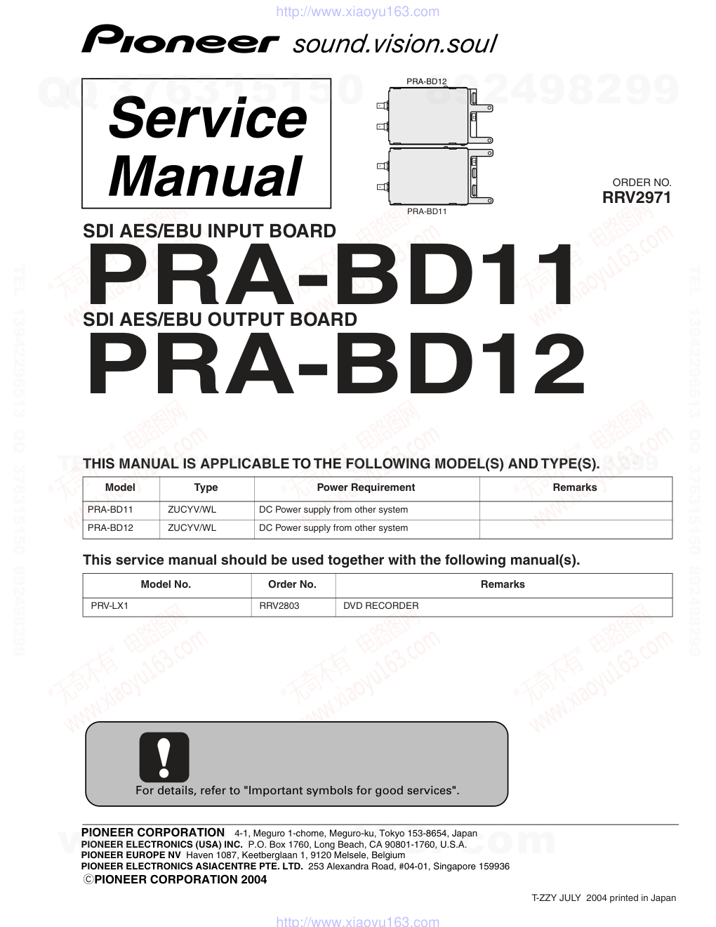
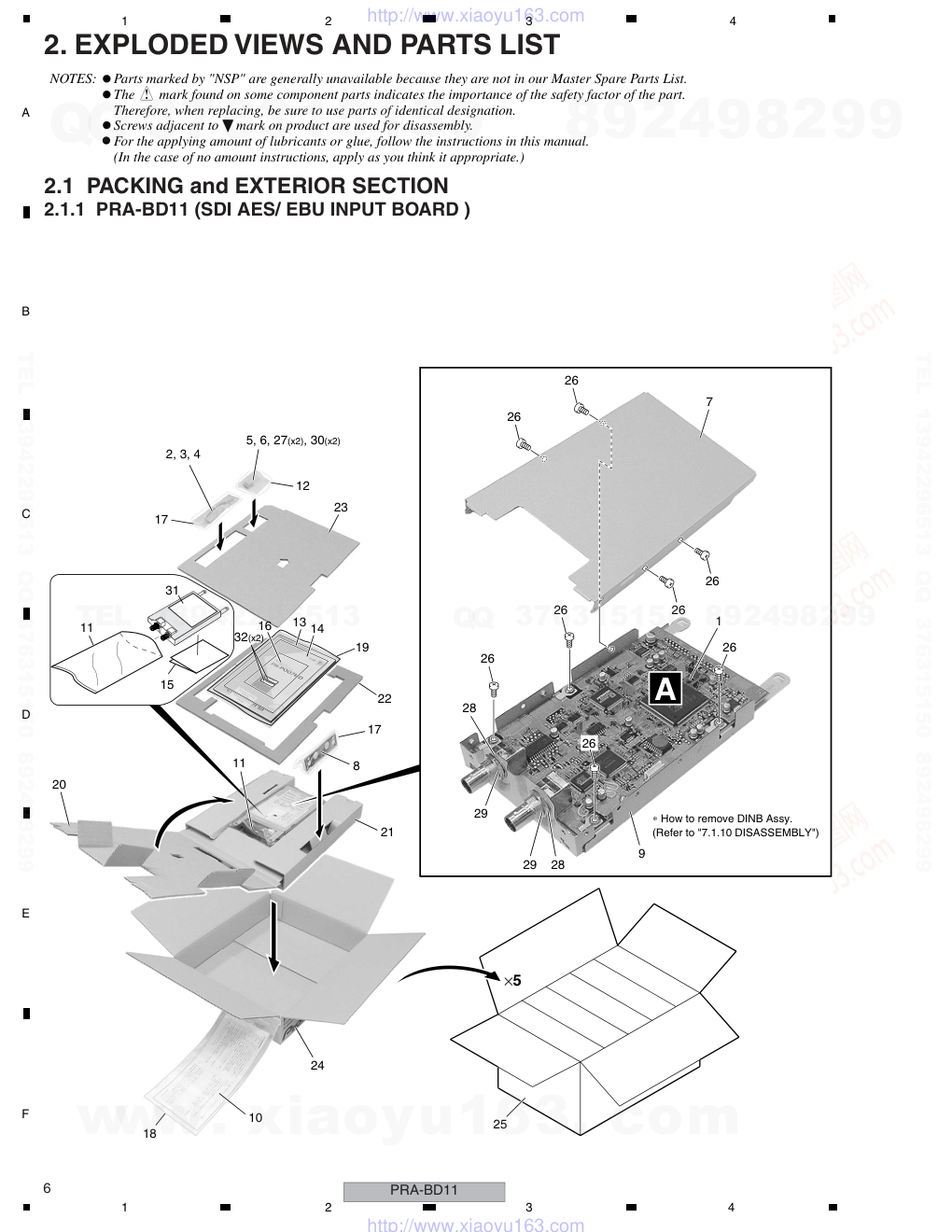
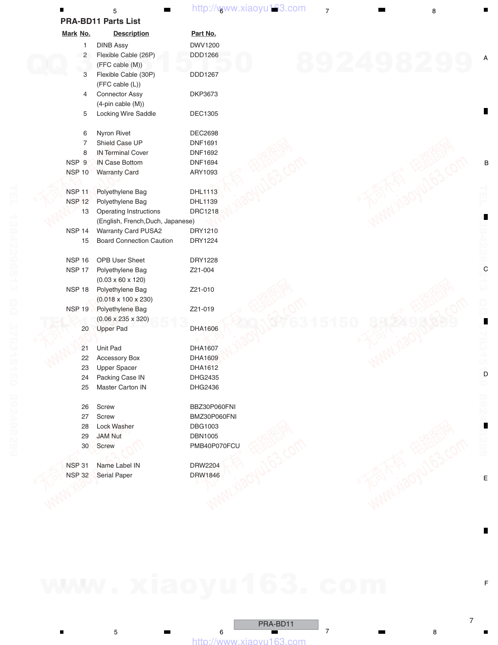
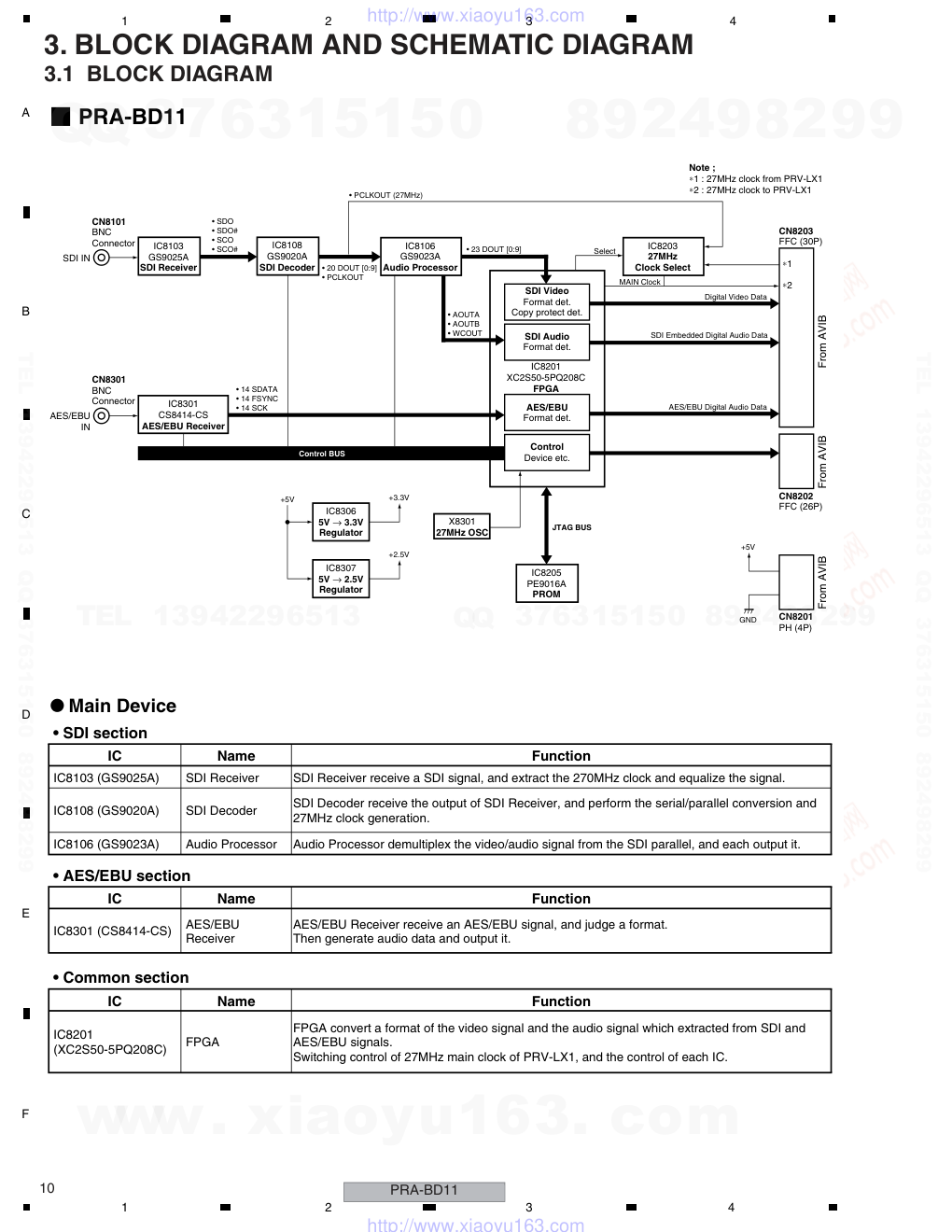
先锋PIONEER PRA-BD11音响电路图
 "先锋PIONEER PRA-BD11音响电路图-0")
 "先锋PIONEER PRA-BD11音响电路图-1")
 "先锋PIONEER PRA-BD11音响电路图-2")
 "先锋PIONEER PRA-BD11音响电路图-3")
 "先锋PIONEER PRA-BD11音响电路图-4")
 "先锋PIONEER PRA-BD11音响电路图-5")
 "先锋PIONEER PRA-BD11音响电路图-6")
 "先锋PIONEER PRA-BD11音响电路图-7")
 "先锋PIONEER PRA-BD11音响电路图-8")
 "先锋PIONEER PRA-BD11音响电路图-9")
ORDER NO. PIONEER CORPORATION 4-1, Meguro 1-chome, Meguro-ku, Tokyo 153-8654, Japan PIONEER ELECTRONICS (USA) INC. P.O. Box 1760, Long Beach, CA 90801-1760, U.S.A. PIONEER EUROPE NV Haven 1087, Keetberglaan 1, 9120 Melsele, Belgium PIONEER ELECTRONICS ASIACENTRE PTE. LTD. 253 Alexandra Road, #04-01, Singapore 159936 PIONEER CORPORATION 2004 PRA-BD12 PRA-BD11 RRV2971 SDI AES/EBU INPUT BOARD PRA-BD11 SDI AES/EBU OUTPUT BOARD PRA-BD12 THIS MANUAL IS APPLICABLE TO THE FOLLOWING MODEL(S) AND TYPE(S). This service manual should be used together with the following manual(s). Model Type Power Requirement Remarks PRA-BD11 ZUCYV/WL DC Power supply from other system PRA-BD12 ZUCYV/WL DC Power supply from other system Model No. Order No. Remarks PRV-LX1 RRV2803 DVD RECORDER For details, refer to "Important symbols for good services". T-ZZY JULY 2004 printed in Japan www. xiaoyu163. com QQ 376315150 9 9 2 8 9 4 2 9 8 TEL 13942296513 9 9 2 8 9 4 2 9 8 0 5 1 5 1 3 6 7 3 Q Q TEL 13942296513 QQ 376315150 892498299 TEL 13942296513 QQ 376315150 892498299 http://www.xiaoyu163.com PRA-BD11 2 1 2 3 4 1 2 3 4 C D F A B E SAFETY INFORMATION This service manual is intended for qualified service technicians ; it is not meant for the casual do-it- yourselfer. Qualified technicians have the necessary test equipment and tools, and have been trained to properly and safely repair complex products such as those covered by this manual. Improperly performed repairs can adversely affect the safety and reliability of the product and may void the warranty. If you are not qualified to perform the repair of this product properly and safely, you should not risk trying to do so and refer the repair to a qualified service technician. WARNING This product contains lead in solder and certain electrical parts contain chemicals which are known to the state of California to cause cancer, birth defects or other reproductive harm. Health & Safety Code Section 25249.6 – Proposition 65 www. xiaoyu163. com QQ 376315150 9 9 2 8 9 4 2 9 8 TEL 13942296513 9 9 2 8 9 4 2 9 8 0 5 1 5 1 3 6 7 3 Q Q TEL 13942296513 QQ 376315150 892498299 TEL 13942296513 QQ 376315150 892498299 http://www.xiaoyu163.com PRA-BD11 3 5 6 7 8 5 6 7 8 C D F A B E CONTENTS 1. SPECIFICATIONS.............................................................................................................................................4 2. EXPLODED VIEWS AND PARTS LIST.............................................................................................................6 2.1 PACKING and EXTERIOR SECTION.........................................................................................................6 2.1.1 PRA-BD11 (SDI AES/ EBU INPUT BOARD ) ......................................................................................6 2.1.2 PRA-BD12 (SDI AES/ EBU OUTPUT BOARD) ...................................................................................8 3. BLOCK DIAGRAM AND SCHEMATIC DIAGRAM ..........................................................................................10 3.1 BLOCK DIAGRAM....................................................................................................................................10 3.2 OVERALL CONNECTION DIAGRAM ......................................................................................................12 3.3 [PRA-BD11]: DINB ASSY (1/4).................................................................................................................14 3.4 [PRA-BD11]: DINB ASSY (2/4).................................................................................................................16 3.5 [PRA-BD11]: DINB ASSY (3/4).................................................................................................................18 3.6 [PRA-BD11]: DINB ASSY (4/4).................................................................................................................20 3.7 [PRA-BD12]: DOOB ASSY (1/2)...............................................................................................................22 3.8 [PRA-BD12]: DOOB ASSY (2/2)...............................................................................................................24 4. PCB CONNECTION DIAGRAM ......................................................................................................................26 5. PCB PARTS LIST............................................................................................................................................30 6. ADJUSTMENT ................................................................................................................................................31 7. GENERAL INFORMATION .............................................................................................................................32 7.1 DIAGNOSIS..............................................................................................................................................32 7.1.1 [PRA-BD11]: HOW TO OPERATION CHECK ....................................................................................32 7.1.2 [PRA-BD11]: LIST OF STATUS LED INDICATION ............................................................................37 7.1.3 [PRA-BD11]: EXTERNAL I/F SPECIFICATIONS ...............................................................................38 7.1.4 [PRA-BD11]: TROUBLESHOOTING ..................................................................................................39 7.1.5 [PRA-BD12]: HOW TO OPERATION CHECK ....................................................................................45 7.1.6 [PRA-BD12]: LIST OF STATUS LED INDICATION ............................................................................48 7.1.7 [PRA-BD12]: TEST MODE .................................................................................................................50 7.1.8 [PRA-BD12]: OPERATION CHECK OF THE ASSY...........................................................................51 7.1.9 [PRA-BD12]: TROUBLESHOOTING ..................................................................................................52 7.1.10 DISASSEMBLY ................................................................................................................................59 7.1.11 INSTALLATION.................................................................................................................................60 7.2 IC INFORMATION ....................................................................................................................................70 8. PANEL FACILITIES .........................................................................................................................................96 [ Important symbols for good services ] In this manual, the symbols shown-below indicate that adjustments, settings or cleaning should be made securely. When you find the procedures bearing any of the symbols, be sure to fulfill them: 2. Adjustments To keep the original performances of the product, optimum adjustments or specification confirmation is indispensable. In accordance with the procedures or instructions described in this manual, adjustments should be performed. 3. Cleaning For optical pickups, tape-deck heads, lenses and mirrors used in projection monitors, and other parts requiring cleaning, proper cleaning should be performed to restore their performances. 5. Lubricants, glues, and replacement parts Appropriately applying grease or glue can maintain the product performances. But improper lubrication or applying glue may lead to failures or troubles in the product. By following the instructions in this manual, be sure to apply the prescribed grease or glue to proper portions by the appropriate amount.For replacement parts or tools, the prescribed ones should be used. 4. Shipping mode and shipping screws To protect the product from damages or failures that may be caused during transit, the shipping mode should be set or the shipping screws should be installed before shipping out in accordance with this manual, if necessary. 1. Product safety You should conform to the regulations governing the product (safety, radio and noise, and other regulations), and should keep the safety during servicing by following the safety instructions described in this manual. www. xiaoyu163. com QQ 376315150 9 9 2 8 9 4 2 9 8 TEL 13942296513 9 9 2 8 9 4 2 9 8 0 5 1 5 1 3 6 7 3 Q Q TEL 13942296513 QQ 376315150 892498299 TEL 13942296513 QQ 376315150 892498299 http://www.xiaoyu163.com PRA-BD11 4 1 2 3 4 1 2 3 4 C D F A B E 1. SPECIFICATIONS [PRA-BD11] SDI input connectors: Connector configuration ................ BNC (1) Input impedance ............................. 75 Ω Supported video standard .............. SMPTE 259 M-C compliant (270 Mb/S, 525i/625i 4:2:2 component input) Supported audio standard .............. SMPTE 272 M compliant (Linear PCM, 48 kHz, 20-bit, channel 1/2) *1, *2, *3 AES/EBU input connectors: Connector configuration ................. BNC (1) Input impedance ............................. 75 Ω Supported audio standard .............. AES-3ID-1995 compliant (Linear PCM, 48 kHz, 16/18/20 bit, industrial format) ∗1,∗3, ∗4 General: Power supply ................................. +5 V DC (supplied internally by PRV-LX1) Weight ........................................... 0.3 kg Dimensions .................................... 195.5 (W) x 101 (D) x 28.4 (H) mm (including projections) Ambient operating temperature ..... +5 to +35 °C (PRV-LX1 it mounts) Ambient operating humidity ........... 5 to 85 % RH (no condensation) ∗1 Quantization bits input to the PRV-LX1 are converted to 16 bits. ∗2 Audio channel 3/4 input is not supported. SDI audio can only be selected during SDI video input (audio only cannot be selected). ∗3 Compressed audio cannot be input. ∗4 Digital audio input of the CP-1201 consumer format is not supported. [PRA-BD12] SDI output connectors: ∗1 Connector configuration ................. BNC (1) Output impedance .......................... 75 Ω Supported video standard .............. SMPTE 259 M-C compliant (270 Mb/S, 525i/625i 4:2:2 component output) Supported audio standard ............. SMPTE 272 M compliant (Linear PCM, 48 kHz, 20-bit, channel 1/2) ∗2, ∗3 AES/EBU output connectors : ∗1 Connector configuration .................. BNC (1) Output impedance ........................... 75 Ω Supported audio standard ............... AES-3ID-1995 compliant (Linear PCM, 48 kHz industrial format) ∗2, ∗3 General: Power supply .................................. +5 V DC (supplied internally by PRV-LX1) Weight ............................................ 0.3 kg Dimensions ...................................... 195.5 (W) x 101 (D) x 28.4 (H) mm (including projections) Ambient operating temperature ...... +5 to +35 °C (PRV-LX1 it mounts) Ambient operating humidity ............ 5 to 85% RH (no condensation) ∗1 Video/audio data is not output when playing back content containing signals preventing unauthorized copying to protect copyright holders, etc. The PRA-BD12 does not support through output of SDI and AES/EBU signals via the PRA-BD11 (SDI AES/EBU input board). ∗2 Compressed audio cannot be output. ∗3 Output of the CP-1201 consumer format is not supported. • Specifications and design are subject to possible modification without notice. www. xiaoyu163. com QQ 376315150 9 9 2 8 9 4 2 9 8 TEL 13942296513 9 9 2 8 9 4 2 9 8 0 5 1 5 1 3 6 7 3 Q Q TEL 13942296513 QQ 376315150 892498299 TEL 13942296513 QQ 376315150 892498299 http://www.xiaoyu163.com PRA-BD11 5 5 6 7 8 5 6 7 8 C D F A B E (DDD1267) (DDD1266) (DKP3673) (DKP3674) (26pin) (30pin) • 4-pin cable (M) • 4-pin cable (L) Short cable (1pin color : White) (approx. 90 mm) Long cable (1pin color : Blue) (approx. 130mm) • FFC cable (M) (DDD1267) • FFC cable (L) • FFC cable (L) Narrow Wide (30pin) Wide Accessories PRA-BD11 PRA-BD12 • IN Terminal Cover..1 (DNF1692) • OUT Terminal Cover..1 (DNF1693) Cushion (DEC2716) Cable Support (DNG1090) Binder (ZCA-SKB90BK) Ferrite Core (DTH1188) Cable Sheet (DEC2710) • Operating Instructions (DRC1218) • Warranty Card (For Japan) • Warranty Card PUSA2 • Board Connection Caution (DRY1224) • OPB User Sheet (For U.S.) (DRY1228) • Screw..x2 (PMB40P070FCU) • Screw..x2 (BMZ30P060FNI) • Screw..x2 (PMB40P070FCU) • Screw..x2 (BMZ30P060FNI) • Nyron Rivet...x1 (DEC2698) • Nyron Rivet...x1 (DEC2698) • Operating Instructions (DRC1218) • Warranty Card (For Japan) • Warranty Card PUSA2 • Board Connection Caution (DRY1224) • OPB User Sheet (For U.S.) (DRY1228) • Locking Wire Saddle..x1 (DEC1305) • Locking Wire Saddle..x1 (DEC1305) Double-sided tape side www. xiaoyu163. com QQ 376315150 9 9 2 8 9 4 2 9 8 TEL 13942296513 9 9 2 8 9 4 2 9 8 0 5 1 5 1 3 6 7 3 Q Q TEL 13942296513 QQ 376315150 892498299 TEL 13942296513 QQ 376315150 892498299 http://www.xiaoyu163.com PRA-BD11 6 1 2 3 4 1 2 3 4 C D F A B E 2. EXPLODED VIEWS AND PARTS LIST 2.1 PACKING and EXTERIOR SECTION 2.1.1 PRA-BD11 (SDI AES/ EBU INPUT BOARD ) Parts marked by "NSP" are generally unavailable because they are not in our Master Spare Parts List. The mark found on some component parts indicates the importance of the safety factor of the part. Therefore, when replacing, be sure to use parts of identical designation. Screws adjacent to mark on product are used for disassembly. For the applying amount of lubricants or glue, follow the instructions in this manual. (In the case of no amount instructions, apply as you think it appropriate.) NOTES: ×5 26 2, 3, 4 5, 6, 27(x2), 30(x2) 13 14 16 32(x2) 17 12 7 23 19 15 11 31 17 9 28 29 28 26 26 26 26 26 26 26 29 1 21 10 24 25 18 8 22 20 11 ∗ How to remove DINB Assy. (Refer to "7.1.10 DISASSEMBLY") A www. xiaoyu163. com QQ 376315150 9 9 2 8 9 4 2 9 8 TEL 13942296513 9 9 2 8 9 4 2 9 8 0 5 1 5 1 3 6 7 3 Q Q TEL 13942296513 QQ 376315150 892498299 TEL 13942296513 QQ 376315150 892498299 http://www.xiaoyu163.com PRA-BD11 7 5 6 7 8 5 6 7 8 C D F A B E PRA-BD11 Parts List Mark No. Description Part No. 1 DINB Assy DWV1200 2 Flexible Cable (26P) DDD1266 (FFC cable (M)) 3 Flexible Cable (30P) DDD1267 (FFC cable (L)) 4 Connector Assy DKP3673 (4-pin cable (M)) 5 Locking Wire Saddle DEC1305 6 Nyron Rivet DEC2698 7 Shield Case UP DNF1691 8 IN Terminal Cover DNF1692 NSP 9 IN Case Bottom DNF1694 NSP 10 Warranty Card ARY1093 NSP 11 Polyethylene Bag DHL1113 NSP 12 Polyethylene Bag DHL1139 13 Operating Instructions DRC1218 (English, French,Duch, Japanese) NSP 14 Warranty Card PUSA2 DRY1210 15 Board Connection Caution DRY1224 NSP 16 OPB User Sheet DRY1228 NSP 17 Polyethylene Bag Z21-004 (0.03 x 60 x 120) NSP 18 Polyethylene Bag Z21-010 (0.018 x 100 x 230) NSP 19 Polyethylene Bag Z21-019 (0.06 x 235 x 320) 20 Upper Pad DHA1606 21 Unit Pad DHA1607 22 Accessory Box DHA1609 23 Upper Spacer DHA1612 24 Packing Case IN DHG2435 25 Master Carton IN DHG2436 26 Screw BBZ30P060FNI 27 Screw BMZ30P060FNI 28 Lock Washer DBG1003 29 JAM Nut DBN1005 30 Screw PMB40P070FCU NSP 31 Name Label IN DRW2204 NSP 32 Serial Paper DRW1846 www. xiaoyu163. com QQ 376315150 9 9 2 8 9 4 2 9 8 TEL 13942296513 9 9 2 8 9 4 2 9 8 0 5 1 5 1 3 6 7 3 Q Q TEL 13942296513 QQ 376315150 892498299 TEL 13942296513 QQ 376315150 892498299 http://www.xiaoyu163.com PRA-BD11 8 1 2 3 4 1 2 3 4 C D F A B E 2.1.2 PRA-BD12 (SDI AES/ EBU OUTPUT BOARD) ×5 30 2, 3 4, 5, 31(x2), 34(x2) 6, 7, 11, 12, 35 20 15 8 26 22 16 17 20 20 27 10 32 33 32 30 30 30 30 30 30 30 33 1 24 13 28 29 21 9 25 23 14 19 37(x2) 18 11 36 ∗ How to remove DOOB Assy. (Refer to "7.1.10 DISASSEMBLY") B www. xiaoyu163. com QQ 376315150 9 9 2 8 9 4 2 9 8 TEL 13942296513 9 9 2 8 9 4 2 9 8 0 5 1 5 1 3 6 7 3 Q Q TEL 13942296513 QQ 376315150 892498299 TEL 13942296513 QQ 376315150 892498299 http://www.xiaoyu163.com PRA-BD11 9 5 6 7 8 5 6 7 8 C D F A B E PRA-BD12 Parts List Mark No. Description Part No. 1 DOOB Assy DWV1201 2 Flexible Cable (30P) DDD1267 (FFC cable (L)) 3 Connector Assy DKP3674 (4-pin cable (M)) 4 Locking Wire Saddle DEC1305 5 Nyron Rivet DEC2698 6 Cable Sheet DEC2710 7 Cushion DEC2716 8 Shield Case UP DNF1691 9 OUT Terminal Cover DNF1693 NSP 10 OUT Case Bottom DNF1695 11 Cable Support DNG1090 12 Ferrite Core DTH1188 NSP 13 Warranty Card ARY1093 NSP 14 Polyethylene Bag DHL1113 NSP 15 Polyethylene Bag DHL1139 16 Operating Instructions DRC1218 (English, French,Duch, Japanese) NSP 17 Warranty Card PUSA2 DRY1210 18 Board Connection Caution DRY1224 NSP 19 OPB User Sheet DRY1228 NSP 20 Polyethylene Bag Z21-004 (0.03 x 60 x 120) NSP 21 Polyethylene Bag Z21-010 (0.018 x 100 x 230) NSP 22 Polyethylene Bag Z21-019 (0.06 x 235 x 320) 23 Upper Pad DHA1606 24 Unit Pad DHA1607 25 Accessory Box DHA1609 26 Upper Spacer DHA1612 27 Bracket Spacer DHA1617 28 Packing Case OUT DHG2437 29 Master Carton OUT DHG2438 30 Screw BBZ30P060FNI 31 Screw BMZ30P060FNI 32 Lock Washer DBG1003 33 JAM Nut DBN1005 34 Screw PMB40P070FCU 35 Binder (SKB-90BK) ZCA-SKB90BK NSP 36 Name Label OUT DRW2205 NSP 37 Serial Paper DRW1846 www. xiaoyu163. com QQ 376315150 9 9 2 8 9 4 2 9 8 TEL 13942296513 9 9 2 8 9 4 2 9 8 0 5 1 5 1 3 6 7 3 Q Q TEL 13942296513 QQ 376315150 892498299 TEL 13942296513 QQ 376315150 892498299 http://www.xiaoyu163.com PRA-BD11 10 1 2 3 4 1 2 3 4 C D F A B E 3. BLOCK DIAGRAM AND SCHEMATIC DIAGRAM 3.1 BLOCK DIAGRAM Main Device • SDI section • AES/EBU section • Common section ∗1 Note ; ∗1 : 27MHz clock from PRV-LX1 ∗2 : 27MHz clock to PRV-LX1 ∗2 IC Name Function IC8103 (GS9025A) SDI Receiver SDI Receiver receive a SDI signal, and extract the 270MHz clock and equalize the signal. IC8108 (GS9020A) SDI Decoder SDI Decoder receive the output of SDI Receiver, and perform the serial/parallel conversion and 27MHz clock generation. IC8106 (GS9023A) Audio Processor Audio Processor demultiplex the video/audio signal from the SDI parallel, and each output it. IC Name Function IC8301 (CS8414-CS) AES/EBU Receiver AES/EBU Receiver receive an AES/EBU signal, and judge a format. Then generate audio data and output it. IC Name Function IC8201 (XC2S50-5PQ208C) FPGA FPGA convert a format of the video signal and the audio signal which extracted from SDI and AES/EBU signals. Switching control of 27MHz main clock of PRV-LX1, and the control of each IC. CN8101 BNC Connector CN8203 FFC (30P) IC8103 GS9025A SDI Receiver • SDO • SDO# • SCO • SCO# • 20 DOUT [0:9] • PCLKOUT • AOUTA • AOUTB • WCOUT • 23 DOUT [0:9] Digital Video Data MAIN Clock Select • PCLKOUT (27MHz) SDI IN IC8108 GS9020A SDI Decoder IC8205 PE9016A PROM X8301 27MHz OSC IC8106 GS9023A Audio Processor IC8306 5V → 3.3V Regulator IC8203 27MHz Clock Select IC8201 XC2S50-5PQ208C FPGA CN8301 BNC Connector IC8301 CS8414-CS AES/EBU Receiver • 14 SDATA • 14 FSYNC • 14 SCK AES/EBU IN SDI Embedded Digital Audio Data AES/EBU Digital Audio Data +5V +5V +3.3V IC8307 5V → 2.5V Regulator +2.5V GND SDI Video Format det. Copy protect det. SDI Audio Format det. AES/EBU Format det. Control Device etc. Control BUS JTAG BUS CN8202 FFC (26P) CN8201 PH (4P) From AVIB From AVIB From AVIB PRA-BD11 www. xiaoyu163. com QQ 376315150 9 9 2 8 9 4 2 9 8 TEL 13942296513 9 9 2 8 9 4 2 9 8 0 5 1 5 1 3 6 7 3 Q Q TEL 13942296513 QQ 376315150 892498299 TEL 13942296513 QQ 376315150 892498299 http://www.xiaoyu163.com PRA-BD11 11 5 6 7 8 5 6 7 8 C D F A B E Main Device Block, IC Function Regulator block Generate +3.3V and +2.5V power from +5V power supplied by AVIB Clock control block Generate 27MHz and 36.864MHz clocks for video and audio from 27MHz clock supplied by AVIB, and supply to each IC Clock generation block Generate 18.432MHz that are a basic clock for RS-232C I/F of FPGA Work with asynchronization for a audio 36.864MHz clock of the clock control block Generate 27MHz to use for the simple signal generator function for board check FPGA (IC8611) FPGA Communication with RS-232C for inside status display Communication control with AVIB Operation setting of each IC in the board and the LED control for status display CCIR656 video data control 3-wires audio data control Sampling frequency 96kHz of audio data convert to 48kHz Generate 6.144MHz and 12.288MHz clocks for audio (dividing by 36.864MHz clock) Simple signal generator function for board check (switching by a DIP switch) Digital audio transmitter (IC8614) Convert 3-wires audio data from the FPGA into AES/EBU data Embedded audio processor (IC8613) Superimposing the 3-wires audio data from the FPGA on the CCIR656 video data from the FPGA, and convert 8-bit to 10-bit. Digital video serializer (IC8617) Convert 10-bit CCIR656 video data from the embedded audio processor to SDI serial data Regulator Block Clock Control Block Clock Generate Block IC8611 XC2S50-5PQ208C FPGA IC8613 GS9023A Embedded Audio Processor IC8617 GS7032 Digital Video Serializer IC8614 AK4103A Digital Audio Transmitter Control Control CCIR656 Video CCIR656 Video CCIR656 Video (Audio Superimposing) SDI Data 3-wires Audio 3-wires Audio 6.144MHz Clock 3-wires Audio +5V +3.3V +3.3V +5V +5V +2.5V +3.3V +2.5V CN8601 PH (4P) From AVIB From AVIB CN8610 FFC (7P) CN8602 FFC (30P) CN8608 BNC Connector SDI OUT AES/EBU Data RS-232C Control CN8609 BNC Connector AES/EBU OUT RS-232C PRA-BD12 27MHz Clock 27MHz Clock 12.288MHz Clock 27MHz Clock 18.432MHz Clock 36.864MHz Clock www. xiaoyu163. com QQ 376315150 9 9 2 8 9 4 2 9 8 TEL 13942296513 9 9 2 8 9 4 2 9 8 0 5 1 5 1 3 6 7 3 Q Q TEL 13942296513 QQ 376315150 892498299 TEL 13942296513 QQ 376315150 892498299 http://www.xiaoyu163.com PRA-BD11 12 1 2 3 4 1 2 3 4 C D F A B E 3.2 OVERALL CONNECTION DIAGRAM ÷ When ordering service parts, be sure to refer to "EXPLODED VIEWS and PARTS LIST" or "PCB PARTS LIST". ÷ The > mark found on some component parts indicates the importance of the safety factor of the part. Therefore, when replacing, be sure to use parts of identical designation. ÷ : The power supply is shown with the marked box. A 1/4 - A 4/4 PRV-LX1 AVIB ASSY (DWV1198) A B 1/2 - B 2/2 B 1 2 3 4 OFF FSK DINB ASSY (DWV1200) PRA-BD11 PRA-BD12 DOOB ASSY (DWV1201) To. PCIB ASSY (CN2104, CN2103) To. JKIB ASSY (CN7613) To. JKIB ASSY (CN7611) To. JKIB ASSY (CN7402) To. PWRB ASSY (CN2) To. DECB ASSY (CN1651, CN1811) To. PCIB ASSY (CN2101) S8602 (DIP- SW) AKN7032 DKN1192 DKN1192 www. xiaoyu163. com QQ 376315150 9 9 2 8 9 4 2 9 8 TEL 13942296513 9 9 2 8 9 4 2 9 8 0 5 1 5 1 3 6 7 3 Q Q TEL 13942296513 QQ 376315150 892498299 TEL 13942296513 QQ 376315150 892498299 http://www.xiaoyu163.com PRA-BD11 13 5 6 7 8 5 6 7 8 C D F A B E Connection and Pin Function DINB ASSY (DWV1200) CN8201 ↔ AVIB ASSY (CN3203) CN8202 ↔ AVIB ASSY (CN5502) CN8203 ↔ AVIB ASSY (CN5501) CN8101 ↔ External Unit CN8301 ↔ External Unit No. Name I/O Function 1, 4 GND − Ground 2, 3 +5V − +5V power supply input No. Name I/O Function 2 AES_LRCK O LR clock output for AES/EBU 3 AES_DAI O Data output for AES/EBU 4 AES_BCK O Audio clock output for AES/EBU 6 SDI_LRCK O LR clock output for SDI embedded audio 7 SDI_DAI O Data output for SDI embedded audio 8 SDI_BCK O Audio clock output for SDI embedded audio 11-25 SDI [0 : 7] O SDI digital video signal output 27 CLK_27MSDI_SEL O 27MHz clock output 29 CLK_27MAVIB I 27MHz clock input CN8610 ↔ RS-232C jig GGF1348 (DVD interface jig for service) CN8602 ↔ AVIB ASSY (CN5503) No. Name I/O Function 1 DINB_EXIST O A signal to judge installation of DINB H : DINB is installed. 2 SDI_VALID O Lock to the SDI signal, and a signal to show whether the signal is a component SD signal or not. H : Lock to a SDI signal, and signal format is valid. L : SDI signal is invalid or there is no input. 3 SDI_NP O Inputted video signal to SDI to show whether the signal is NTSC or PAL. H : NTSC , L : PAL 4 SDI_LOCK O Signal to show whether the audio signal that is included in SDI signal is locked or not. H : Locks to the embedded audio L : Unlocks to the embedded audio 5 SDI_RST I DINB system reset signal input 6 AES_ERROR O A signal to show whether the error of AES/EBU signal exists. H : There is no error with AES/EBU signal. L : There is an error with AES/EBU signal. 7 MODE_SEL I Set the operating mode of the AES/EBU receiver. H : Clock output (master) mode L : Clock input (slave) mode 8-25 TP [1 : 16] O FPGA test signal output No. Name I/O Function 1 GND I GND input for SDI 2 SDI I SDI input Signal level is PECL (800mVp-p) at input No. Name I/O Function 1 GND I GND input for AES/EBU 2 AES/EBU I AES/EBU input Signal level is 1Vp-p at input CN8608 ↔ External Unit (SDI input) DOOB ASSY (DWV1201) CN8601 ↔ AVIB ASSY (CN3204) No. Name I/O Function 1, 4 GND − Digital ground 2, 3 +5V − +5V power supply input CN8609 ↔ External Unit (AES/EBU input) Switch 1 Switch 2 Switch 3 Switch 4 OFF side ON side 1 2 3 4 1 2 3 4 5 6 7 8 OFF FSK S8602 (DIP switch) No. Name I/O Function 1 GND − Digital ground 2 N.C. − Reserve 3 SDO_ENA I/O DOOB system control signal (LVTTL level) 4 XRESET I System reset input (LVTTL level) 5 GND − Digital ground 6 SDO_LRCK I 3-line audio LR clock input (LVTTL level) 7 SDO_DAI I 3-line audio data input (LVTTL level) 8 SDO_BCK I 3-line audio bit clock input (LVTTL level) 9 N.C. − Reserve 10 GND − Digital ground 11 SDO_D0 I CCIR Rec656 data input (LVTTL level) 12 GND − Digital ground 13 SDO_D1 I CCIR Rec656 data input (LVTTL level) 14 GND − Digital ground 15 SDO_D2 I CCIR Rec656 data input (LVTTL level) 16 GND − Digital ground 17 SDO_D3 I CCIR Rec656 data input (LVTTL level) 18 GND − Digital ground 19 SDO_D4 I CCIR Rec656 data input (LVTTL level) 20 GND − Digital ground 21 SDO_D5 I CCIR Rec656 data input (LVTTL level) 22 GND − Digital ground 23 SDO_D6 I CCIR Rec656 data input (LVTTL level) 24 GND − Digital ground 25 SDO_D7 I CCIR Rec656 data input (LVTTL level) 26 GND − Digital ground 27 N.C. − Reserve 28 GND − Digital ground 29 27MSDO I 27MHz clock input (LVTTL level) 30 GND − Digital ground No. Name I/O Function 1 GND − Analog ground 2 DATA O Output (800mVp-p ± 10%, output impedance 75Ω, 270Mbps) No. Name I/O Function 1 GND − Analog ground 2 DATA O AES/EBU output (1.0Vp-p ± 20%, output impedance 75Ω, 3.072Mbps) No. Name I/O Function 1 N.C. − Reserve 2 GND − Digital ground 3 +5V − +5V power supply input 4 CTS I Reserve (RS-232C CTS inut at LVTTL level) 5 RTS O Reserve (RS-232C RTS inut at LVTTL level) 6 RxD I Reserve (RS-232C RxD inut at LVTTL level) 7 TxD O RS-232C TxD input (LVTTL level) No. Name Function Land Setting for Land 1 Test mode setting OFF : Normal operation ON : Test mode TP8660 OFF : Open ON : L (GND) 2 NTSC/PAL setting at test mode OFF : Video is NTSC at test mode ON : Video is PAL at test mode TP8661 OFF : Open ON : L (GND) 3, 4 Reserve − − − www. xiaoyu163. com QQ 376315150 9 9 2 8 9 4 2 9 8 TEL 13942296513 9 9 2 8 9 4 2 9 8 0 5 1 5 1 3 6 7 3 Q Q TEL 13942296513 QQ 376315150 892498299 TEL 13942296513 QQ 376315150 892498299 http://www.xiaoyu163.com PRA-BD11 14 1 2 3 4 1 2 3 4 C D F A B E 3.3 [PRA-BD11]: DINB ASSY (1/4) A 1/4 A 1/4 DINB ASSY (DWV1200) 2/4 A 2/4 A 2/4 A 2/4, 4/4 A 2/4, 4/4 A 2/4, 3/4 A www. xiaoyu163. com QQ 376315150 9 9 2 8 9 4 2 9 8 TEL 13942296513 9 9 2 8 9 4 2 9 8 0 5 1 5 1 3 6 7 3 Q Q TEL 13942296513 QQ 376315150 892498299 TEL 13942296513 QQ 376315150 892498299 http://www.xiaoyu163.com PRA-BD11 15 5 6 7 8 5 6 7 8 C D F A B E A 1/4 2/4 A 2/4, 4/4 A 2/4, 4/4 A 2/4, 4/4 A 2/4, 4/4 A 2/4 A 4/4 A 2/4, 3/4 A www. xiaoyu163. com QQ 376315150 9 9 2 8 9 4 2 9 8 TEL 13942296513 9 9 2 8 9 4 2 9 8 0 5 1 5 1 3 6 7 3 Q Q TEL 13942296513 QQ 376315150 892498299 TEL 13942296513 QQ 376315150 892498299 http://www.xiaoyu163.com PRA-BD11 16 1 2 3 4 1 2 3 4 C D F A B E 3.4 [PRA-BD11]: DINB ASSY (2/4) A 2/4 A 2/4 DINB ASSY (DWV1200) 3/4 A 3/4, 4/4 A 1/4, 4/4 A 1/4, 4/4 A 1/4 A 1/4 A 1/4, 3/4 A 1/4, 4/4 A 1/4, 4/4 A 3/4 A 1/4 A 1/4 A www. xiaoyu163. com QQ 376315150 9 9 2 8 9 4 2 9 8 TEL 13942296513 9 9 2 8 9 4 2 9 8 0 5 1 5 1 3 6 7 3 Q Q TEL 13942296513 QQ 376315150 892498299 TEL 13942296513 QQ 376315150 892498299 http://www.xiaoyu163.com PRA-BD11 17 5 6 7 8 5 6 7 8 C D F A B E A 2/4 AVIB ASSY CN3203 AVIB ASSY CN5502 AVIB ASSY CN5501 1/4, 3/4 A 3/4 A www. xiaoyu163. com QQ 376315150 9 9 2 8 9 4 2 9 8 TEL 13942296513 9 9 2 8 9 4 2 9 8 0 5 1 5 1 3 6 7 3 Q Q TEL 13942296513 QQ 376315150 892498299 TEL 13942296513 QQ 376315150 892498299 http://www.xiaoyu163.com PRA-BD11 18 1 2 3 4 1 2 3 4 C D F A B E 3.5 [PRA-BD11]: DINB ASSY (3/4) A 3/4 A 3/4 DINB ASSY (DWV1200) 2/4 A 2/4 A 2/4 A 2/4, 4/4 A 2/4, 4/4 A 1/4, 2/4 A www. xiaoyu163. com QQ 376315150 9 9 2 8 9 4 2 9 8 TEL 13942296513 9 9 2 8 9 4 2 9 8 0 5 1 5 1 3 6 7 3 Q Q TEL 13942296513 QQ 376315150 892498299 TEL 13942296513 QQ 376315150 892498299 http://www.xiaoyu163.com PRA-BD11 19 5 6 7 8 5 6 7 8 C D F A B E A 3/4 www. xiaoyu163. com QQ 376315150 9 9 2 8 9 4 2 9 8 TEL 13942296513 9 9 2 8 9 4 2 9 8 0 5 1 5 1 3 6 7 3 Q Q TEL 13942296513 QQ 376315150 892498299 TEL 13942296513 QQ 376315150 892498299 http://www.xiaoyu163.com PRA-BD11 20 1 2 3 4 1 2 3 4 C D F A B E 3.6 [PRA-BD11]: DINB ASSY (4/4) A 4/4 A 4/4 DINB ASSY (DWV1200) 1/4, 2/4 A 1/4, 2/4 A 1/4, 2/4 A 1/4, 2/4 A 2/4, 3/4 A 1/4 A www. xiaoyu163. com QQ 376315150 9 9 2 8 9 4 2 9 8 TEL 13942296513 9 9 2 8 9 4 2 9 8 0 5 1 5 1 3 6 7 3 Q Q TEL 13942296513 QQ 376315150 892498299 TEL 13942296513 QQ 376315150 892498299 http://www.xiaoyu163.com PRA-BD11 21 5 6 7 8 5 6 7 8 C D F A B E www. xiaoyu163. com QQ 376315150 9 9 2 8 9 4 2 9 8 TEL 13942296513 9 9 2 8 9 4 2 9 8 0 5 1 5 1 3 6 7 3 Q Q TEL 13942296513 QQ 376315150 892498299 TEL 13942296513 QQ 376315150 892498299 http://www.xiaoyu163.com PRA-BD11 22 1 2 3 4 1 2 3 4 C D F A B E 3.7 [PRA-BD12]: DOOB ASSY (1/2) B 1/2 B 1/2 DOOB ASSY (DWV1201) AVIB ASSY CN3204 AVIB ASSY CN5503 2/2 B www. xiaoyu163. com QQ 376315150 9 9 2 8 9 4 2 9 8 TEL 13942296513 9 9 2 8 9 4 2 9 8 0 5 1 5 1 3 6 7 3 Q Q TEL 13942296513 QQ 376315150 892498299 TEL 13942296513 QQ 376315150 892498299 http://www.xiaoyu163.com PRA-BD11 23 5 6 7 8 5 6 7 8 C D F A B E B 1/2 2/2 B 2/2 B 2/2 B 2/2 B 2/2 B 2/2 B 2/2 B 2/2 B www. xiaoyu163. com QQ 376315150 9 9 2 8 9 4 2 9 8 TEL 13942296513 9 9 2 8 9 4 2 9 8 0 5 1 5 1 3 6 7 3 Q Q TEL 13942296513 QQ 376315150 892498299 TEL 13942296513 QQ 376315150 892498299 http://www.xiaoyu163.com PRA-BD11 24 1 2 3 4 1 2 3 4 C D F A B E 3.8 [PRA-BD12]: DOOB ASSY (2/2) B 2/2 B 2/2 DOOB ASSY (DWV1201) 1/2 B 1/2 B 1/2 B 1/2 B 1/2 B 1/2 B 1/2 B 1/2 B 1/2 B 1/2 B 1/2 B www. xiaoyu163. com QQ 376315150 9 9 2 8 9 4 2 9 8 TEL 13942296513 9 9 2 8 9 4 2 9 8 0 5 1 5 1 3 6 7 3 Q Q TEL 13942296513 QQ 376315150 892498299 TEL 13942296513 QQ 376315150 892498299 http://www.xiaoyu163.com PRA-BD11 25 5 6 7 8 5 6 7 8 C D F A B E B 2/2 1/2 B 1/2 B 1/2 B 1/2 B www. xiaoyu163. com QQ 376315150 9 9 2 8 9 4 2 9 8 TEL 13942296513 9 9 2 8 9 4 2 9 8 0 5 1 5 1 3 6 7 3 Q Q TEL 13942296513 QQ 376315150 892498299 TEL 13942296513 QQ 376315150 892498299 http://www.xiaoyu163.com PRA-BD11 26 1 2 3 4 1 2 3 4 C D F A B E 4. PCB CONNECTION DIAGRAM 4.1 [PRA-BD11]: DINB ASSY TP8127 TP8126 1 3 5 4 1 0 1 2 3 4 5 6 7 8 9 0 1 2 3 0 0 1 C B A TP8125 TP8128 TP8201 TP8208 TP8207 TP8206 TP8211 TP8209 TP8205 TP8204 TP8202 3 1 5 4 R 14 1 7 8 1 11 12 22 23 33 34 44 3 1 2 1 20 21 40 41 60 61 80 1 3 4 5 1 3 4 5 3 1 2 1 25 26 50 51 75 76 100 1 10 11 20 1 7 8 14 1 10 11 20 1 10 11 20 1 10 11 20 1 6 1 10 11 20 1 3 4 5 1 4 5 8 28 15 14 1 1 7 8 14 1 3 4 5 F8301 TP8306 C8146 R8109 C8319 R8128 R8126 IC8312 IC8103 TP8305 C8312 IC8306 TP8308 F8302 C8308 C8315 IC8108 C8113 C8104 C8118 R8114 C8124 R8122 C8125 R8115 C8110 R8113 R8112 L8109 R8218 C8109 R8110 C8112 TP8307 C8320 R8310 R8124 R8125 C8318 C8306 F8104 R8104 R8103 R8142 TP8132 TP8133 TP8134 TP8136 TP8137 TP8139 TP8138 TP8140 IC8110 R8141 R8140 R8105 R8106 L8104 TP8301 R8304 L8105 R8307 L8110 IC8109 IC8307 R8302 C8321 C8317 KN8301 L8206 R8273 R8277 R8269 R8308 R8306 R8301 TP8479 TP8302 TP8320 TP8319 TP8318 TP8315 TP8309 TP8314 KN8304 TP8117 TP8118 R8102 TP8129 TP8131 TP8124 TP8135 F8102 IC8106 IC8104 TP8109 TP8111 TP8112 TP8114 TP8115 TP8113 TP8110 F8105 F8106 R8116 R8120 C8122 IC8105 R8117 F8108 R8144 R8146 C8114 C8130 C8128 F8101 C8106 F8107 IC8101 F8206 IC8205 F8103 IC8102 KN8303 R8123 TP8486 TP8328 TP8326 TP8325 TP8327 F8201 R8303 TP8304 TP8324 C8307 R8280 R8278 R8279 F8202 D8301 F8203 F8204 TP8310 TP8311 TP8312 TP8313 TP8321 C8314 TP8322 TP8317 TP8323 TP8485 C8313 C8316 R8212 R8213 R8249 R8248 R8256 R8201 R8210 R8207 R8206 C8271 CN8204 R8211 R8205 R8204 R8202 IC8204 R8270 R8271 R8274 R8275 R8276 TP8256 TP8255 TP8254 TP8253 TP8252 TP8251 TP8250 TP8245 R8259 TP8249 TP8244 TP8243 TP8214 R8220 TP8213 R8219 TP8212 R8215 KN8302 IC8311 TP8316 L8205 R8272 IC8203 D8302 C8304 C8303 R8305 IC8301 TP8484 TP8483 IC8309 IC8308 R8323 D8305 C8325 F8303 R8315 TP8481 TP8480 CN8101 CN8301 TH8301 TH8302 R8309 F8305 F8304 C8142 R8121 R8107 R8108 TP8285 D8306 TP8284 TP8119 TP8120 TP8121 TP8122 TP8123 R8145 R8132 R8133 R8127 R8134 TP8482 R8131 R8130 R8129 TP8103 R8147 R8148 R8149 R8139 R8143 R8138 TP8116 R8153 R8267 TP8258 R8268 TP8259 TP8240 TP8239 TP8238 TP8237 TP8235 TP8234 TP8233 TP8231 TP8230 TP8229 TP8226 TP8225 TP8224 TP8223 R8221 R8223 R8224 TP8215 TP8217 TP8218 TP8219 R8225 TP8221 R8203 TP8257 TP8247 TP8248 TP8246 R8214 TP8210 IC8201 R8281 R8282 R8283 R8284 R8285 34 23 33 1 44 11 22 1 H A B 11 TP8284 CLK_27MSDI_SEL GNDD GNDD GNDD GNDD GNDD 4 14 8 14 12 8 100 1 10 11 1 3 80 5 10 1 X X I Z 50 11 Y 208 +5.0V 26 40 21 20 1 61 60 41 4 20 11 10 1 20 4 5 1 3 1 7 1 8 14 1 10 11 20 6 1 2GND 1+3.3V 6TDS 5TDI 4TDO 3TCK 7 +5.0V 51 Z AES IN 20 SDI IN GNDD 5IN 5M2 5M1 TP8285 27M_GEN Y C A C B +3.3V +2.5V H +5.0V +3.3V DWV1200- 1 5 1 25 3 4 75 10 I 7 2 20 2 94V-0 DINB DNP2093-A 1 1 +5.0V FPM V0 GNDD GNDD GNDD +5.0V 1 14 15 28 76 +2.5V 1 8 1 5 157 156 105 104 53 52 1 SIDE A A DINB ASSY A (DNP2093-A) IC8103 IC8108 IC8205 IC8311 IC8312 IC8101 IC8102 IC8301 IC8309 IC8308 IC8201 IC8204 IC8203 IC8105 IC8109 IC8106 IC8306 IC8110 IC8307 IC8104 NOTE FOR PCB DIAGRAMS : 1. Part numbers in PCB diagrams match those in the schematic diagrams. 2. A comparison between the main parts of PCB and schematic diagrams is shown below. 3. The parts mounted on this PCB include all necessary parts for several destinations. For further information for respective destinations, be sure to check with the schematic diagram. 4. View point of PCB diagrams. Symbol In PCB Diagrams Symbol In Schematic Diagrams Part Name B C E D D G G S S B C E B C E D G S B C E B C E B C E Transistor Transistor with resistor Field effect transistor Resistor array 3-terminal regulator Capacitor Connector P.C.Board Chip Part SIDE A SIDE B www. xiaoyu163. com QQ 376315150 9 9 2 8 9 4 2 9 8 TEL 13942296513 9 9 2 8 9 4 2 9 8 0 5 1 5 1 3 6 7 3 Q Q TEL 13942296513 QQ 376315150 892498299 TEL 13942296513 QQ 376315150 892498299 http://www.xiaoyu163.com PRA-BD11 27 5 6 7 8 5 6 7 8 C D F A B E 1 4 TP8242 TP8241 TP8236 TP8232 TP8228 TP8227 TP8222 TP8220 TP8216 1 30 FC ICT 1 26 1 5 3 4 1 5 3 4 1 4 2 3 1 4 1 30 1 26 5 4 3 1 5 4 3 1 1 7 8 14 4 3 1 2 C8302 C8218 D8308 D8303 C8219 TP8102 R8118 C8105 R8119 C8117 C8116 C8115 C8119 C8103 C8111 C8108 C8136 C8102 C8141 C8212 C8211 CN8201 C8225 C8226 C8230 C8301 C8134 D8106 C8140 C8139 D8105 C8145 C8137 C8131 TP8105 TP8104 TP8101 C8107 C8143 C8126 C8135 C8129 C8127 C8133 C8138 C8144 C8123 C8120 C8121 C8209 C8101 R8290 C8326 F8205 R8289 C8214 C8224 C8223 C8327 C8213 C8210 C8216 C8228 C8237 C8254 C8255 C8257 C8243 C8203 C8233 C8221 C8204 C8206 C8207 C8205 C8202 C8201 C8208 C8217 C8229 C8244 C8245 C8256 C8252 C8253 C8258 C8215 C8227 C8242 R8250 R8247 R8243 R8238 R8234 R8233 R8229 R8226 R8222 C8268 C8248 C8249 C8250 C8251 C8259 C8260 C8261 C8262 C8263 C8264 C8265 C8266 C8269 C8270 C8247 C8246 R8208 R8209 C8241 C8240 C8239 C8238 C8236 C8235 C8234 C8232 CN8203 D8307 C8231 C8267 C8222 C8220 C8323 C8322 D8304 CN8202 R8111 C8272 C8273 D8205 D8206 D8207 F8207 F8208 IC8206 IC8207 IC8208 R8216 R8217 R8286 R8287 R8288 D8102 X8301 D8103 A AES/EBU INPUT 2 1.GND 2.SDI 2.AES/EBU 1.GND 2 SDI INPUT C 1 14 1 GNDD A 8 1 7 3.+5V 2.+5V 1.GND 4.GND B DOWNSIDE B C GNDD GNDD GNDD LED3 LED2 +3.3V +5.0V CN8201 PC LED1 CONTACT SIDE B A DINB ASSY A (DNP2093-A) AVIB ASSY CN5501 CN8203 AVIB ASSY CN5502 CN8202 AVIB ASSY CN3203 CN8201 IC8208 IC8206 IC8207 www. xiaoyu163. com QQ 376315150 9 9 2 8 9 4 2 9 8 TEL 13942296513 9 9 2 8 9 4 2 9 8 0 5 1 5 1 3 6 7 3 Q Q TEL 13942296513 QQ 376315150 892498299 TEL 13942296513 QQ 376315150 892498299 http://www.xiaoyu163.com PRA-BD11 28 1 2 3 4 1 2 3 4 C D F A B E 4.2 [PRA-BD12]: DOOB ASSY R 1 52 53 104 105 156 157 208 1 10 11 20 1 4 2 3 1 26 1 6 1 10 11 20 1 3 5 4 1 11 12 22 23 33 34 44 1 2 1 26 1 26 1 12 13 24 1 3 5 4 4 8 1 5 1 0 1 2 3 4 5 6 7 8 9 0 1 2 3 0 0 1 C B A 3 1 2 3 1 2 1 10 11 20 4 3 1 2 1 26 6 1 1 10 11 20 1 3 4 5 1 3 4 5 1 11 12 22 23 33 34 44 1 25 26 50 51 75 76 100 5 1 2 6 1 26 1 26 1 12 13 24 1 3 4 5 1 4 5 8 KN8601 TP8610 TP8609 TP8606 TP8608 TP8607 IC8602 IC8601 F8601 IC8611 IC8610 X8601 C8622 R8655 CN8603 C8664 CN8604 C8601 C8603 C8610 C8611 C8606 C8607 C8663 C8605 C8602 C8612 C8609 TH8601 C8633 C8632 R8654 R8662 R8661 R8659 R8656 R8658 R8657 R8652 R8651 R8649 R8660 R8653 R8650 R8647 R8648 R8646 R8642 C8604 R8638 R8637 R8636 R8635 IC8609 VC8601 R8618 R8619 C8620 IC8606 R8623 R8624 C8624 F8603 F8604 C8625 R8625 IC8607 C8623 F8605 C8629 C8621 TP8601 TP8604 R8643 R8644 R8645 TP8605 TP8603 TP8602 D8606 R8729 D8610 D8609 R8725 R8722 CN8609 R8728 R8727 R8726 R8723 R8721 C8675 F8610 CN8608 L8602 R8716 R8713 C8680 C8679 C8683 R8712 R8715 C8682 R8714 F8608 IC8617 C8681 R8710 R8677 R8678 IC8613 C8665 L8603 CN8607 R8672 R8709 R8682 CN8606 C8678 R8668 IC8614 R8707 R8711 R8742 R8741 IC8620 R8740 R8732 D8611 S8602 R8745 KN8604 KN8602 KN8603 R8627 TP8612 TP8659 TP8611 FPM V0 OFF POSITION 3 2 1 5 TP8670 TP8616 TP8663 100 26 76 50 75 1 51 25 NTSC/PAL TP8646 TP8648 TP8647 GND TP8613 TP8615 TP8651 TP8654 +5V GND TP8644 TP8638 TP8645 TP8649 TP8632 TP8634 DOOB TP8636 18.432MHz 3.Reserve TP8666 TP8664 GND 1 TP8662 ON:TEST MODE 4.Reserve TP8660 SIDE OF TEST MODE TP8657 ON:PAL TEST TP8614 TP8641 TP8665 TxD TP8667 TP8643 TP8669 TP8640 5 TP8627 TP8631 TP8633 TP8629 TP8625 TP8621 TP8617 TP8661 TP8620 TP8624 TP8628 TP8635 TP8618 TP8622 TP8626 TP8623 TP8619 TP8630 2.OFF:NTSC TEST 4 +5V +3.3V +3.3V +2.5V CLK +5V GND GND GND 1 2 AES/EBU 2 SDI GND GND 3 1 CLK 27MHz 36.864MHz CLK 1.OFF:NORMAL DWV1201- DNP2094-A SIDE A B DOOB ASSY B (DNP2094-A) IC8617 IC8613 IC8614 IC8611 IC8609 IC8606 IC8620 IC8607 IC8602 IC8610 IC8601 www. xiaoyu163. com QQ 376315150 9 9 2 8 9 4 2 9 8 TEL 13942296513 9 9 2 8 9 4 2 9 8 0 5 1 5 1 3 6 7 3 Q Q TEL 13942296513 QQ 376315150 892498299 TEL 13942296513 QQ 376315150 892498299 http://www.xiaoyu163.com PRA-BD11 29 5 6 7 8 5 6 7 8 C D F A B E 1 30 1 5 3 4 1 4 8 1 5 4 1 10 11 20 1 7 8 14 1 7 8 14 1 7 16 1 8 9 1 30 5 4 3 1 1 4 1 4 5 8 1 7 8 14 1 10 11 20 1 7 8 14 1 7 8 14 1 3 4 5 1 7 R8633 IC8608 CN8602 D8603 IC8603 R8604 C8613 CN8601 D8604 D8602 C8645 C8631 C8608 R8601 R8603 D8601 F8602 R8640 R8639 C8646 C8643 C8644 C8642 C8641 C8640 C8639 C8638 C8636 C8637 C8634 C8635 C8661 C8660 C8659 C8658 C8657 C8656 C8655 C8654 C8652 C8653 C8651 C8650 C8648 C8649 C8647 R8606 R8605 R8610 C8614 F8606 R8634 C8630 R8607 R8608 R8609 IC8604 C8615 R8611 R8612 C8616 R8615 R8614 D8605 R8613 IC8605 C8619 R8620 R8621 R8622 C8617 R8617 R8616 C8618 C8628 C8627 C8626 R8628 R8629 R8631 R8632 R8630 R8626 R8641 IC8612 C8662 R8664 R8663 R8665 C8674 R8681 R8671 R8670 R8669 C8669 C8668 C8670 R8673 R8674 C8667 C8671 R8676 R8675 R8666 C8666 C8672 C8673 R8679 IC8616 IC8615 C8676 R8684 R8683 F8607 R8680 R8667 C8684 R8737 R8733 R8730 D8612 IC8621 X8602 D8614 D8613 D8617 D8615 D8616 R8746 Q8602 Q8603 Q8601 CN8610 R8691 R8743 R8744 R8747 7 1 8 4 5 1 3 14 1 8 9 16 GND ICT FC GND 1 +5V SDI OUT +2.5V +5V LED5 LED4 LED1 +5V PC SIDE LED2 1 2 +3.3V 2 AES/EBU OUT DOWN CONTACT CONTACT TP8639 LED3 LED6 SIDE B B DOOB ASSY B (DNP2094-A) AVIB ASSY CN5503 CN8602 AVIB ASSY CN3204 CN8601 IC8615 IC8616 IC8604 IC8612 IC8603 IC8605 IC8608 IC8621 Q8603 Q8601 Q8602 www. xiaoyu163. com QQ 376315150 9 9 2 8 9 4 2 9 8 TEL 13942296513 9 9 2 8 9 4 2 9 8 0 5 1 5 1 3 6 7 3 Q Q TEL 13942296513 QQ 376315150 892498299 TEL 13942296513 QQ 376315150 892498299 http://www.xiaoyu163.com PRA-BD11 30 1 2 3 4 1 2 3 4 C D F A B E 5. PCB PARTS LIST Parts marked by "NSP" are generally unavailable because they are not in our Master Spare Parts List. The mark found on some component parts indicates the importance of the safety factor of the part. Therefore, when replacing, be sure to use parts of identical designation. When ordering resistors, first convert resistance values into code form as shown in the following examples. Ex.1 When there are 2 effective digits (any digit apart from 0), such as 560 ohm and 47k ohm (tolerance is shown by J=5%, and K=10%). Ex.2 When there are 3 effective digits (such as in high precision metal film resistors). 5 6 1 4 7 3 R 5 0 1 R 0 5 6 2 1 NOTES: 560 Ω 47k Ω 0.5 Ω 1 Ω RD1/4PU J RD1/4PU J RN2H K RS1P K 56 x 10 1 47 x 10 3 R50 1R0 561 473 5.62k Ω RN1/4PC F 562 x 10 1 5621 Mark No. Description Part No. LIST OF ASSEMBLIES [PRA-BD11] 1..DINB ASSY DWV1200 [PRA-BD12] 1..DOOB ASSY DWV1201 • PRA-BD11 Mark No. Description Part No. A DINB ASSY SEMICONDUCTORS >IC8306 BA033FP >IC8307 BA25BC0FP IC8301 CS8414-CS IC8108 GS9020A IC8106 GS9023A IC8103 GS9025A IC8205 PE9016A IC8104 PLL1700E IC8308 PST9124N IC8203 SN74AHC2G53HDCT IC8312 TC74ACT32F IC8101, IC8102, IC8204 TC74LCX541FT IC8105 TC74LCX74FT IC8309 TC74VHC14FT IC8208 TC74VHCU04FT IC8109, IC8110 TC7SET08FU IC8311 TC7SH00F IC8206, IC8207 TC7SLU04F IC8201 XC2S50-5PQ208C D8105, D8106, D8305, D8306 1SS355 D8205-D8207, D8303, D8304 SML-310DT D8301, D8302 UDZS5R1(B) >TH8301, TH8302 MINISMDC075F COILS AND FILTERS F8101-F8108, F8201-F8208 DTF1070 F8304, F8305 DTF1070 L8109 LCTAW15NJ2520 F8301-F8303 VTH1040 L8104, L8105, L8110, L8205, L8206 VTL1079 CAPACITORS C8112 CCSRCH101J50 C8272, C8273 CCSRCH150J50 C8106, C8113, C8128, C8130, C8306 CEVW100M16 C8308, C8313, C8314, C8316, C8317 CEVW100M16 C8319, C8320, C8325 CEVW100M16 C8122 CEVW101M6R3 C8101-C8103, C8105, C8107-C8111 CKSRYB103K50 C8114, C8119-C8121, C8123 CKSRYB103K50 C8126, C8127, C8129, C8131 CKSRYB103K50 C8133-C8146, C8201-C8209 CKSRYB103K50 C8215-C8217, C8221, C8227-C8229 CKSRYB103K50 C8233, C8237, C8242-C8245 CKSRYB103K50 C8252-C8258, C8267, C8268, C8271 CKSRYB103K50 C8303, C8304, C8315, C8321-C8323 CKSRYB103K50 C8326, C8327 CKSRYB103K50 C8115-C8118, C8301, C8302, C8318 CKSRYB104K16 C8124 CKSRYB153K50 C8312 CKSRYB224K10 C8104 CKSRYB472K50 C8307 CKSRYB683K16 C8125 DCG1034 RESISTORS R8138, R8139, R8143, R8147-R8149 RAB4C0R0J R8203, R8214, R8215, R8218-R8221 RAB4C0R0J R8223-R8225, R8301-R8304 RAB4C0R0J R8306, R8307 RAB4C0R0J R8118 RS1/16S3650F R8110, R8112, R8113, R8305 RS1/16S75R0F Other Resistors RS1/16S###J OTHERS CN8202 (26P CONNECTOR) AKN7032 CN8101, CN8301 (BNC CONNECTOR) DKN1163 CN8203 (30P FFC CONNECTOR) DKN1192 CN8201 (PH CONNECTOR) S4B-PH-SM3 KN8301-KN8304 VNF1109 (EARTH METAL FITTING) X8301 (27.000MHz) VSS1146 Mark No. Description Part No. www. xiaoyu163. com QQ 376315150 9 9 2 8 9 4 2 9 8 TEL 13942296513 9 9 2 8 9 4 2 9 8 0 5 1 5 1 3 6 7 3 Q Q TEL 13942296513 QQ 376315150 892498299 TEL 13942296513 QQ 376315150 892498299 http://www.xiaoyu163.com PRA-BD11 31 5 6 7 8 5 6 7 8 C D F A B E • PRA-BD12 6. ADJUSTMENT • There is no information to be shown in this chapter. Mark No. Description Part No. B DOOB ASSY SEMICONDUCTORS IC8614 AK4103AVF >IC8602 BA033FP >IC8601 BA25BC0FP IC8608 BU2288FV IC8617 GS7032 IC8613 GS9023A IC8610 PE9017A IC8603 PST9124N IC8605, IC8616 TC74LCX32FT IC8609 TC74LCX541FT IC8615 TC74VHC125FT IC8612 TC74VHC541FT IC8606 TC7SLU04F IC8607, IC8621 TC7SZ125FU IC8620 TC7SZ126FU IC8604 TC7WU04FU IC8611 XC2S50-5PQ208C Q8601-Q8603 DTA124EUA D8603, D8604 1SS355 D8601, D8602, D8605 SML-310DT D8612-D8617 SML-310PT >TH8601 MINISMDM160 COILS AND FILTERS F8602-F8608, F8610 DTF1070 L8603 DTL1116 L8602 LCTAW27NJ2520 F8601 VTH1040 CAPACITORS C8608, C8615, C8622, C8623 CCSRCH150J50 C8603, C8604, C8606, C8610, C8611 CEVW100M16 C8629, C8632, C8633, C8663, C866511CEVW100M16 C8675, C8678 CEVW100M16 C8602, C8605, C8607, C8609 CKSRYB103K50 C8612-C8614, C8616-C8619, C8621 CKSRYB103K50 C8624-C8628, C8630, C8631 CKSRYB103K50 C8634-C8662, C8664, C8666-C8674 CKSRYB103K50 C8676, C8679-C8682, C8684 CKSRYB103K50 C8620 CKSRYB104K16 C8683 CKSRYB105K6R3 RESISTORS R8607-R8609, R8641-R8645 RAB4C220J R8647-R8656, R8659-R8664 RAB4C220J R8675, R8676 RAB4C220J R8710 RS1/16S3000F R8726, R8727 RS1/16S33R0F R8712, R8713, R8721, R8728 RS1/16S56R0F R8711, R8714-R8716 RS1/16S75R0F Other Resistors RS1/16S###J SWITCH S8602 BSH1015 OTHERS CN8608, CN8609 (BNC CONNECTOR) DKN1163 CN8602 (30P FFC CONNECTOR) DKN1192 CN8601 (PH CONNECTOR) S4B-PH-SM3 CN8610 (7P FFC CONNECTOR ) VKN1411 KN8601-KN8604 VNF1109 (EARTH METAL FITTING) X8601 (27.000MHz) VSS1146 X8602 (18.432MHz) VSS1194 Mark No. Description Part No. www. xiaoyu163. com QQ 376315150 9 9 2 8 9 4 2 9 8 TEL 13942296513 9 9 2 8 9 4 2 9 8 0 5 1 5 1 3 6 7 3 Q Q TEL 13942296513 QQ 376315150 892498299 TEL 13942296513 QQ 376315150 892498299 http://www.xiaoyu163.com PRA-BD11 32 1 2 3 4 1 2 3 4 C D F A B E 7. GENERAL INFORMATION 7.1 DIAGNOSIS 7.1.1 [PRA-BD11]: HOW TO OPERATION CHECK 1. Equipment necessary for operational checking of the main unit • PRV-LX1 (Product -jig 1 for checking): The PRA-BD11 is to be mounted. • PRV-LX1 (Product -jig 2 for checking): The PRA-BD12 (product -jig) is to be mounted. • PRA-BD12 (product -jig) • AV amplifier & Speaker • GGV1035 (Test disc: DVDT-001) • DKP3673 (4 pin cable (M)) • DDD1266 ( FFC cable (M)) • DDD1267 ( FFC cable (L)) • BNC - BNC cable: 2 cables • TV monitor 2. About video and audio signals to be used for operational checking of the main unit Play back the GGV1035 Test Disc with the PRV-LX1 (Product -jig 2). The formats of signals to be used for inspection of the main unit are as follows: • SDI : 270-MHz SDI signal with 525/60i embedded audio • AES/EBU : Professional-format, 48-kHz sampling frequency AES/EBU signal PRA-BD11 PRV-LX1 AVIB: CN5501 AVIB: CN5502 AVIB: CN3203 ~ Ÿ ! Preview composite output waveform from the PRV-LX1 (J model) when a 100% color-bar signal is input to the SDI video input connector Preview RCA output waveform from the PRV-LX1 (J model) when a sine waveform signal at 1 kHz with -20 dB Fs is input to the SDI audio input and AES/EBU input connectors 3. Inspection of the main unit 3-1. Mount the PRA-BD11 on the PRV-LX1 (Product -jig 1) and connect it with the PRV-LX1 (Product -jig 2) using the 4-pin PH cable: DKP3673 (!), 26-pin FFC cable: DDD1266 (~), and 30-pin FFC cable: DDD1267 (Ÿ). www. xiaoyu163. com QQ 376315150 9 9 2 8 9 4 2 9 8 TEL 13942296513 9 9 2 8 9 4 2 9 8 0 5 1 5 1 3 6 7 3 Q Q TEL 13942296513 QQ 376315150 892498299 TEL 13942296513 QQ 376315150 892498299 http://www.xiaoyu163.com PRA-BD11 33 5 6 7 8 5 6 7 8 C D F A B E 3-2. Connect the composite output and RCA output of the PRV-LX1 (Product -jig 2) to an oscilloscope to check their signal waveforms. Also connect the loop-through output signals from the oscilloscope to a TV monitor and audio amplifier to monitor video and audio signals. Then start up the PRV-LX1 (Product -jig 2). An example of connection is shown in the figure below. 3-3. Start up the PRV-LX1 (Product -jig 1) with the PRA-BD11 mounted. After startup, connect the SDI and AES/EBU signals to Product -jig 2. Check LEDs 1-3 after signal connection. Composite input TV monitor RCA input Audio amplifier Speakers Oscilloscope RCA output Composite output Loop through output PRV-LX1 (Product 2) SDI output AES/EBU output www. xiaoyu163. com QQ 376315150 9 9 2 8 9 4 2 9 8 TEL 13942296513 9 9 2 8 9 4 2 9 8 0 5 1 5 1 3 6 7 3 Q Q TEL 13942296513 QQ 376315150 892498299 TEL 13942296513 QQ 376315150 892498299 http://www.xiaoyu163.com PRA-BD11 34 1 2 3 4 1 2 3 4 C D F A B E 3-4. After confirming that all the LEDs are lit, set the video and audio input to SDI on the Function menu. Press the Preview button of the PRV-LX1 (Product -jig 1) to monitor and check that the video and audio signals are output normally. After the confirmation, press the Preview button again to cancel Preview mode. Examples of settings on the Function menu: 3-5. On the Function menu set the video input to SDI and audio input to AES/EBU. Press the Preview button of the PRV-LX1 (Product -jig 1) to monitor and check that the video and audio signals are output normally. After the confirmation, press the Preview button again to cancel Preview mode. 3-6. Set the power to the PRV-LX1 (Product -jig 1) to Standby then set the Power switch on the rear panel to OFF. Remove the PRA-BD11 then close the cable-securing lid for the FFC connectors. Examples of settings on the Function menu: www. xiaoyu163. com QQ 376315150 9 9 2 8 9 4 2 9 8 TEL 13942296513 9 9 2 8 9 4 2 9 8 0 5 1 5 1 3 6 7 3 Q Q TEL 13942296513 QQ 376315150 892498299 TEL 13942296513 QQ 376315150 892498299 http://www.xiaoyu163.com PRA-BD11 35 5 6 7 8 5 6 7 8 C D F A B E SIDE A DINB ASSY A IC8312 IC8103 IC8108 IC8110 IC8109 TP8479 IC8106 IC8104 IC8105 IC8101 IC8205 IC8102 TP8486 TP8328 TP8326 TP8325 TP8327 TP8324 TP8485 IC8204 IC8311 IC8301 TP8484 TP8483 TP8286 TP8287 TP8288 IC8309 IC8308 TP8481 TP8480 TP8285 TP8482 TP8487 IC8201 TP8284 CLK_27MSDI_SEL GNDD GNDD GNDD GNDD GNDD +5.0V +5.0V GNDD TP8285 27M_GEN C +3.3V 1 2 GNDD GNDD GNDD +5.0V +2.5V 1 5M2 5M1 5IN 4. Major points to measure, such as those for the power and ground Major points to measure Pin No. Signal Name Description Pin No. Signal Name Description TP8324 TP8325 TP8326 TP8327 TP8328 GNDD Ground TP8473 +5VA 5.0V power supply for the analog system TP8474 +2VD 2.5V power supply for the digital system TP8282 5M1 Power supply after branching TP8472 +3VD 3.3V power supply for the digital system TP8287 5M2 Power supply after branching TP8487 +5VD 5.0V power supply for the digital system TP8286 5IN Power supply before branching www. xiaoyu163. com QQ 376315150 9 9 2 8 9 4 2 9 8 TEL 13942296513 9 9 2 8 9 4 2 9 8 0 5 1 5 1 3 6 7 3 Q Q TEL 13942296513 QQ 376315150 892498299 TEL 13942296513 QQ 376315150 892498299 http://www.xiaoyu163.com PRA-BD11 36 1 2 3 4 1 2 3 4 C D F A B E SIDE A DINB ASSY A IC8312 IC8103 IC8108 IC8110 IC8109 TP8479 IC8106 IC8104 IC8105 IC8101 IC8205 IC8102 TP8486 TP8328 TP8326 TP8325 TP8327 TP8324 TP8485 IC8204 IC8311 IC8301 TP8484 TP8483 TP8286 TP8287 TP8288 IC8309 IC8308 TP8481 TP8480 TP8285 TP8482 TP8487 IC8201 TP8284 CLK_27MSDI_SEL GNDD GNDD GNDD GNDD GNDD +5.0V +5.0V GNDD TP8285 27M_GEN C +3.3V 1 2 GNDD GNDD GNDD +5.0V +2.5V 1 5M2 5M1 5IN Checker chips are provided for various power supplies, ground, and clock signals for easier measuring with an oscilloscope using a probe. 5. Points to check during servicing Points to check Pin No. Signal Name Description Pin No. Signal Name Description TP8483 TP8484 TP8485 TP8486 GNDD Ground TP8284 CLK_27M SDI_SEL 27MHz signal reproduced from the SDI signal, or when there is no signal input, a return signal of the 27MHz signal from the PRV-LX1 (Measurement must be conducted when the PRV-LX1 is connected with the PRA-BD11) TP8482 +2VD 2.5V power supply for the digital system TP8285 27M_GEN Built-in 27MHz clock generator TP8480 +3VD 3.3V power supply for the digital system TP8479 +5VD 5.0V power supply for the digital system TP8481 +5VA 5.0V power supply for the analog system www. xiaoyu163. com QQ 376315150 9 9 2 8 9 4 2 9 8 TEL 13942296513 9 9 2 8 9 4 2 9 8 0 5 1 5 1 3 6 7 3 Q Q TEL 13942296513 QQ 376315150 892498299 TEL 13942296513 QQ 376315150 892498299 http://www.xiaoyu163.com PRA-BD11 37 5 6 7 8 5 6 7 8 C D F A B E 7.1.2 [PRA-BD11]: LIST OF STATUS LED INDICATION LED 3 LED 2 LED 1 Show the status indication by LEDs in the following tables. LEDs indicate the version of the firmware for about 10 seconds immediately after the power was turne on. Then, shift to each status indication. List of firmware version indications Version Indication LED1 LED2 LED3 1 Lit Unlit Unlit 2 Unlit Lit Unlit 3 Lit Lit Unlit 4 Unlit Unlit Lit 5 Lit Unlit Lit List of status indications +3.3V +3.3V power supply (TH8302, +3.3V regulator BA033 output) OK +5.0V +5V power supply (TH8301) OK LED1 unlit .0Test mode, or GS9023A in failure LED1 lit The SDI audio signals (Ch 1/2) are input. LED1 blink GS9023A operating normally LED2 unlit Either of the following four cases: (1) Test mode, (2) GS9020A in failure, (3) An SDI signal other than 525i/625i component signal (270 Mbps) is being input, or (4) A copy-protected signal is being input. LED2 lit The SDI 525i/625i component signal is being input, and an EDH packet is embedded in the SDI input signal. Both GS9020A and GS9025A are operating normally. LED2 blink No SDI input. GS9020A is operating normally. LED3 unlit When a transmitting machine is not connected: CS8414 in failure When a transmitting machine is connected: A consumer- format signal is input. LED3 lit A 48-kHz Fs AES/EBU signal is being input. LED3 blink Either of two cases: (1) A professional-format signal other than mentioned above is being input, or (2) No AES/EBU input, and CS8414 is operating normally. All the LEDs unlit FPGA in failure www. xiaoyu163. com QQ 376315150 9 9 2 8 9 4 2 9 8 TEL 13942296513 9 9 2 8 9 4 2 9 8 0 5 1 5 1 3 6 7 3 Q Q TEL 13942296513 QQ 376315150 892498299 TEL 13942296513 QQ 376315150 892498299 http://www.xiaoyu163.com PRA-BD11 38 1 2 3 4 1 2 3 4 C D F A B E 7.1.3 [PRA-BD11]: EXTERNAL I/F SPECIFICATIONS The SDI video/audio signals to be inputted to PRA-BD11 and the AES/EBU signals to be inputted to PRA-BD11 are described below. • SDI input connector (CN8101) Type of connector : BNC × 1 Input impedance : 75 ohms Applicable video standard : In compliance with SMPTE 259M-C (270 Mb/S, 525i/625i, 4:2:2, component input) Applicable audio standard : In compliance with SMPTE 272M (Linear PCM 48 kHz, 20 bit, Ch 1/2, convertible into 16-bit mode) • AES/EBU input connector (CN8301) Type of connector : BNC × 1 Input impedance : 75 ohms Applicable audio standard : In compliance with AES-3ID-1995 (Linear PCM 48 kHz, professional format, convertible into 16-bit mode) Notes on the external I/F • SDI input Copy-protection detection function • The following signals can be detected: CGMS-A signals (IEC 61880) contained in VBID in NTSC (J), CGMS-A signals (ETS EN 300294) contained in PAL signals, and CGMS-A signals (IEC 61880) contained in NTSC (U.S.) Line 21. • As to the SDI multiplexed audio signals, only the combined channels 1 and 2 are supported, and input to the channels 3 and 4 is not supported. • Input of signals containing VITC (time code added during the vertical blanking interval) is not supported. • Input of signals containing closed caption is not supported. • When SDI video signals are input, the setting item of "Setup Level" on the Function menu of the PRV-LX1 becomes invalid, and the setting becomes always 0 IRE. • AES/EBU input • Consumer-format (S/P DIF) digital audio input is not supported. • The compressed audio input is not supported. • If analog video signal input is selected, and no corresponding video signal is being input, no sound is recorded even if an audio signal is input. www. xiaoyu163. com QQ 376315150 9 9 2 8 9 4 2 9 8 TEL 13942296513 9 9 2 8 9 4 2 9 8 0 5 1 5 1 3 6 7 3 Q Q TEL 13942296513 QQ 376315150 892498299 TEL 13942296513 QQ 376315150 892498299 http://www.xiaoyu163.com PRA-BD11 39 5 6 7 8 5 6 7 8 C D F A B E 7.1.4 [PRA-BD11]: TROUBLESHOOTING • The following symptoms may be generated, but these are not failures of the unit. Symptom Cause "No SDI video input signal" is displayed. No or incorrect SDI video signals are input. Copy-prohibited SDI video signals are input. "No SDI audio input signal" is displayed. No or incorrect SDI audio signals are input. "No AES/EBU input signal" is displayed. No or incorrect AES/EBU signals are input. An all-black display has been recorded. No or incorrect SDI video signals were being input during recording. A copy-protection signal was detected in the SDI video signals being recorded. No sound has been recorded. No or incorrect SDI audio signals were being input during recording. A copy-protection signal was detected in the SDI video signals being recorded. No or incorrect AES/EBU signals were being input during recording. • Flowchart of LED 1-3 statuses when the PRA-BD11 is operating normally *1: When signals supported by the PRA-BD11 (see "7.1.3 External I/F specifications") are input. *2: See "List of firmware version indications" in "7.1.2 List of Status Indication." Power to the PRV-LX1 ON Firmware version indication by LEDs 1-3 *2 Has approx. 10 seconds elapsed immediately after the power was turned on? LED2 Blink No SDI video input *1 No Yes LED2 lit SDI video input *1 No Yes LED3 Blink AES/EBU input *1 No Yes LED3 lit AES/EBU input *1 No Yes LED1 Blink SDI audio input *1 No Yes LED1 lit SDI audio input *1 No Yes Yes www. xiaoyu163. com QQ 376315150 9 9 2 8 9 4 2 9 8 TEL 13942296513 9 9 2 8 9 4 2 9 8 0 5 1 5 1 3 6 7 3 Q Q TEL 13942296513 QQ 376315150 892498299 TEL 13942296513 QQ 376315150 892498299 http://www.xiaoyu163.com PRA-BD11 40 1 2 3 4 1 2 3 4 C D F A B E • Check the following in Normal Operation mode 10 seconds or more after the power is turned on. • In addition, input a signal according to the setups for each symptom. 1 In a case where LEDs 1-3 are all unlit regardless of the existence of the AES/EBU input signal START • Check the logical state of TP8215. If it is L, check the mounting status of IC8202. • Check the logical state of Pin 4 of IC8308. If it is L, check the mounting status of IC8308. • Check the logical state of Pin 12 of IC8309. If it is L, check the mounting status of IC8309. • Pin 7 of IC8205 is H (reset). • Check the mounting status of IC8205. Check the mounting and operation statuses of IC8307. • Check the mounting and operation statuses of CN8201, R8209, TH8302, F8303, and IC8306, in that order. VCCINT = Pins 13, 28, 38, 66, 76, 91,118, 128, 143, 171, 186 and 196 of IC8201 VCCO = Pins 12, 26, 39, 53, 65, 78, 92, 105, 117, 130, 144, 156, 170, 184, 197 and 208 of IC8201 Check the mounting and operation statuses of F8202. Check the mounting and operation statuses of F8201. Check +2.5 V power supply TP8482= +2.5V +3.3V ? +2.5V ? Check VCCO voltage of IC8201 Check the mounting status of IC8201. Check VCCINT voltage of IC8201 If there is no problem in mounting status, IC8201 may be in failure. IC8201 pin 106 IC8205 pin 10 D8304 L H L H Unlit Lit No Yes No Yes No Yes www. xiaoyu163. com QQ 376315150 9 9 2 8 9 4 2 9 8 TEL 13942296513 9 9 2 8 9 4 2 9 8 0 5 1 5 1 3 6 7 3 Q Q TEL 13942296513 QQ 376315150 892498299 TEL 13942296513 QQ 376315150 892498299 http://www.xiaoyu163.com PRA-BD11 41 5 6 7 8 5 6 7 8 C D F A B E 2 In a case where LED 1 is unlit regardless of the existence of the SDI signal input START Check the logical state of Pin 1 of IC8109. If it is L, check the mounting status of Pin 191 of IC8201. • Check the logical state of TP8215. If it is L, check the mounting status of CN8202. • Check the logical state of Pin 4 of IC8308. If it is L, check the mounting status of IC8308. • Check the logical state of Pin 12 of IC8309. If it is L, check the mounting status of IC8309. Check the mounting and operation statuses of CN8201, R8209, TH8302, F8303, and IC8306, in that order. VDDINT = Pins 1, 17, 26 and 90 of IC8106 VDDIO = Pins 39, 51, 67 and 76 of IC8106 Check the mounting and operation statuses of F8107. +3.3V ? Check the mounting status of IC8106. Check +3.3V power supply If there is no problem in mounting status, IC8106 may be in failure. IC8106 pin 16 IC8109 pin 2 D8304 NG OK Unlit Lit L H L H www. xiaoyu163. com QQ 376315150 9 9 2 8 9 4 2 9 8 TEL 13942296513 9 9 2 8 9 4 2 9 8 0 5 1 5 1 3 6 7 3 Q Q TEL 13942296513 QQ 376315150 892498299 TEL 13942296513 QQ 376315150 892498299 http://www.xiaoyu163.com PRA-BD11 42 1 2 3 4 1 2 3 4 C D F A B E START Check Pins 7, 8, and 9 of IC8101 to see if signals are input. If they are, IC8101 is in failure. Check Pins 12 and 13 of IC8104 to see if signals are output. If they are output, IC8104 is in failure. If no signal is output, check the mounting status of IC8104. If there is no problem with the mounting status, IC8104 is in failure. If a clock signal is not input, check L8104 and R8106. If a clock signal is not output, check the mounting status of IC8105. If a clock signal is not output, check the mounting and operation statuses of L8110 and R8121. Check 12.288MHz clock Check 27MHz clock signal IC8101 pin 12 IC8104 pin 6 Check 6.144MHz clock IC8105 pin 9 IC8106 pin 99 IC8104 pin 6 No Yes No Yes No Yes No Yes No Yes 3 When though a proper SDI signal containing SDI audio signal is input, LED 1 blinks Check "2 In a case where LED 1 is unlit regardless of the existence of the SDI signal input" www. xiaoyu163. com QQ 376315150 9 9 2 8 9 4 2 9 8 TEL 13942296513 9 9 2 8 9 4 2 9 8 0 5 1 5 1 3 6 7 3 Q Q TEL 13942296513 QQ 376315150 892498299 TEL 13942296513 QQ 376315150 892498299 http://www.xiaoyu163.com PRA-BD11 43 5 6 7 8 5 6 7 8 C D F A B E START Check the logical state of Pin 1 of IC8110. If it is L, check the mounting status of Pin 62 of IC8201. Check the mounting and operation statuses of F8102, D8105 and D8106. VDD = Pins 5, 8, 9, 12, 29, 51 and 68 of IC8108 Check the mounting and operation statuses of IC8103 IC8108 pin 31 D8303 Check +5V power supply Check the mounting status of IC8108 +5V ? IC8110 pin 2 Unlit Lit No Yes L H L H 4 When no SDI signal is input, LED 2 is unlit If there is no problem with it, IC8108 may be in failure. • Check the logical state of TP8215. If it is L, check the mounting status of CN8202. • Check the logical state of Pin 4 of IC8308. If it is L, check the mounting statues of IC8308. • Check the logical state of Pin 12 of IC8309. If it is L, check the mounting statuse of IC8309. Input an SDI signal supported by the PRA-BD11 and check the following: • Check that a 270MHz clock signal with voltage swing from about 3.5-4.0 V is output from Pins 28 and 29 of IC8103. • Check that an SDI signal with voltage swing from about 3.2-4.0 V is output from Pins 31 and 32 of IC8103. Check the mounting and operation statuses of CN8201, R8208, TH8301, and F8301, in that order. www. xiaoyu163. com QQ 376315150 9 9 2 8 9 4 2 9 8 TEL 13942296513 9 9 2 8 9 4 2 9 8 0 5 1 5 1 3 6 7 3 Q Q TEL 13942296513 QQ 376315150 892498299 TEL 13942296513 QQ 376315150 892498299 http://www.xiaoyu163.com PRA-BD11 44 1 2 3 4 1 2 3 4 C D F A B E START Check the logical states of Pins 1, 4, 9 and 12 of IC8312. If they are all H, check the mounting statuses of Pins 192, 193, 194, and 195 of IC8201. Check the mounting and operation statuses of F8302. Check the mounting and operation statuses of F8305. Check the mounting and operation statuses of F8304. IC8301 pins 17, 18, 23 and 24 D8303 Check +5V power supply Check the mounting status of IC8301 TP8481= +5V ? Is pin 7 of IC8301 +5V ? Is pin 22 of IC8301 +5V ? IC8311 pin 2 No No No Yes Yes Yes H L H L IC8311 pin 1 H L 5 When no AES/EBU signal is input, LED 3 is unlit If there is no problem in mounting status, IC8301 may be in failure. Check the mounting status of Pin 199 of IC8201. • Check the logical state of TP8215. If it is L, check the mounting status of CN8202. • Check the logical state of Pin 4 of IC8308. If it is L, check the mounting status of IC8308. • Check the logical state of Pin 12 of IC8309. If it is L, check the mounting status of IC8309. Check the mounting and operation statuses of CN8201, R8208, TH8301 and F8301, in that order. Unlit Lit www. xiaoyu163. com QQ 376315150 9 9 2 8 9 4 2 9 8 TEL 13942296513 9 9 2 8 9 4 2 9 8 0 5 1 5 1 3 6 7 3 Q Q TEL 13942296513 QQ 376315150 892498299 TEL 13942296513 QQ 376315150 892498299 http://www.xiaoyu163.com PRA-BD11 45 5 6 7 8 5 6 7 8 C D F A B E 7.1.5 [PRA-BD12]: HOW TO OPERATION CHECK 3-3. Start up the PRV-LX1 (Product -jig 1) with the PRA-BD12 connected. Check the three LEDs for checking the power supply (orange) and six LEDs for checking operations (green). 3-4. Play back the GGV1035 disc on PRV-LX1 (Product -jig 1) and check (preview or recording) the display on the TV monitor connected to PRV-LX1 (Product -jig 2) with PRA-BD11 (product -jig ) to see if video signals are correctly output. Also check the sound to verify that audio signals are correctly output. PRV-LX1 (Product -jig 1) + PRA-BD12 PRV-LX1 (Product -jig 2) + PRA-BD11 (Product) AV Amp. TV monitor Speaker SDI OUT (BNC cable) (BNC cable) AES/EBU OUT Composite Audio 3-2. Connect a TV monitor and AV amplifier to the PRV-LX1 (Product -jig 2), as shown in the figure below, to monitor video and audio signals. PRA-BD12 ~ Ÿ 1. Equipment necessary for operational checking of the main unit • PRV-LX1 (Product -jig 1 for checking): The PRA-BD12 is to be mounted. • PRV-LX1 (Product -jig 2 for checking): The PRA-BD11 (product -jig ) is to be mounted. • PRA-BD11 (product -jig ) • AV amplifier & Speaker • GGV1035 (Test disc: DVDT-001) • DKP3674 (4 pin cable (L)) • DDD1267 ( FFC cable (L)) • BNC - BNC cable: 2 cables • TV monitor 2. About video and audio signals to be used for operational checking of the main unit Play back the GGV1035 Test Disc with the PRV-LX1 (Product -jig 1). 3. Inspection of the main unit 3-1. Mount the PRA-BD12 on the PRV-LX1 (Product -jig 1) and connect it with the PRV-LX1 (Product -jig 2) using the 4-pin PH cable: DKP3674 (~) and 30-pin FFC cable: DDD1267 (Ÿ). www. xiaoyu163. com QQ 376315150 9 9 2 8 9 4 2 9 8 TEL 13942296513 9 9 2 8 9 4 2 9 8 0 5 1 5 1 3 6 7 3 Q Q TEL 13942296513 QQ 376315150 892498299 TEL 13942296513 QQ 376315150 892498299 http://www.xiaoyu163.com PRA-BD11 46 1 2 3 4 1 2 3 4 C D F A B E SIDE A DOOB ASSY B 4. Major points to measure, such as those for the power and ground Major points to measure Pin No. Signal Name Description TP8611 +5V Power supply (input of CN8601) TP8612 GND Ground TP8613 +5V Power supply (after the overcurrent protection circuit passage) TP8614 +3.3V Power supply (convert +5V to +3.3V by regulator) TP8615 +2.5V Power supply (convert +5V to +2.5V by regulator) TP8616 GND Ground TP8635 27MHz CLK 27MHz clock TP8638 36.864MHz CLK 36.864MHz clock (generates from 27MHz clock) TP8640 18.432MHz CLK 18.432MHz clock TP8641 GND TEST MODE NTSC /PAL Ground TP8660 Test mode setting (operate together with S8602 BSH1015 DIP switch 1) TP8661 NTSC/PAL setting in the test mode (operate together with S8602 BSH1015 DIP switch 2) TP8666 +5V Power supply (after the overcurrent protection circuit passage for RS-232C I/F) TP8670 +3.3V Power supply (converts +5V to +3.3V by regulator for RS-232C I/F) TP8662 TxD output for RS-232C I/F (+3.3V CMOS level) TP8667 GND TXD Ground www. xiaoyu163. com QQ 376315150 9 9 2 8 9 4 2 9 8 TEL 13942296513 9 9 2 8 9 4 2 9 8 0 5 1 5 1 3 6 7 3 Q Q TEL 13942296513 QQ 376315150 892498299 TEL 13942296513 QQ 376315150 892498299 http://www.xiaoyu163.com PRA-BD11 47 5 6 7 8 5 6 7 8 C D F A B E SIDE A DOOB ASSY B 5. Points to check during servicing Checker chips are provided for various power supplies, ground, and clock signals for easier measuring with an oscilloscope using a probe. Major points to measure Pin No. Signal Name Description TP8601 +5V Power supply (input of CN8601) TP8602 GND Ground TP8603 +5V Power supply (after the overcurrent protection circuit passage) TP8604 +3.3V Power supply (convert +5V to +3.3V by regulator) TP8605 +2.5V Power supply (convert +5V to +2.5V by regulator) TP8606 GND Ground TP8608 27MHz CLK 27MHz clock TP8607 36.864MHz CLK 36.864MHz clock (generates from 27MHz clock) TP8609 18.432MHz CLK 18.432MHz clock TP8610 GND Ground www. xiaoyu163. com QQ 376315150 9 9 2 8 9 4 2 9 8 TEL 13942296513 9 9 2 8 9 4 2 9 8 0 5 1 5 1 3 6 7 3 Q Q TEL 13942296513 QQ 376315150 892498299 TEL 13942296513 QQ 376315150 892498299 http://www.xiaoyu163.com PRA-BD11 48 1 2 3 4 1 2 3 4 C D F A B E 7.1.6 [PRA-BD12]: LIST OF STATUS LED INDICATION A total of 9 LEDs (3 for checking the power supply and 6 for checking operations) are provided with the PRA-BD12. With these LEDs, the operation status of the PRA-BD12 can be checked after +5 V power is supplied to it. CN8610 LEDs for checking the power supply LEDs for checking operations +3.3V +2.5V LED5 LED3 LED1 LED6 LED4 LED2 +5V CN8601 CN8602 +3.3V +2.5V +5V LED5 LED3 LED1 LED6 LED4 LED2 1. Indications of the LEDs for checking the power supply After +5 V power is supplied to the PRA-BD12, an LED will light if power with the corresponding voltage is being supplied, or it will remain unlit if power with the corresponding voltage not supplied. All three LEDs must be lit for there to be no problem with the PRA-BD12. Each LED corresponds to the following power voltages: +5 V : Power supplied from AVIB Assy through CN8601 (PH connector) then through the overcurrent protection circuit +3.3 V : Power supplied from the +5 V power supply through IC8602 (regulator) +2.5 V : Power supplied from the +5 V power supply through IC8601 (regulator) 2. Firmware version indication by the LEDs for checking operations For about 10 seconds immediately after +5 V power is supplied to the PRA-BD12, six LEDs for checking operations indicate the firmware version with their lighting statuses. LEDs 1-4 represent the place value of ones, and LEDs 5-6 represent the place value of tens. See the table below. Version 1 7 Version LED5 LED3 LED1 LED6 LED4 LED2 Statuses of the LEDs for checking operations Statuses of the LEDs for checking operations LED5 LED3 LED1 LED6 LED4 LED2 2 8 LED5 LED3 LED1 LED6 LED4 LED2 LED5 LED3 LED1 LED6 LED4 LED2 3 9 LED5 LED3 LED1 LED6 LED4 LED2 LED5 LED3 LED1 LED6 LED4 LED2 4 10 LED5 LED3 LED1 LED6 LED4 LED2 LED5 LED3 LED1 LED6 LED4 LED2 5 20 LED5 LED3 LED1 LED6 LED4 LED2 LED5 LED3 LED1 LED6 LED4 LED2 6 30 LED5 LED3 LED1 LED6 LED4 LED2 www. xiaoyu163. com QQ 376315150 9 9 2 8 9 4 2 9 8 TEL 13942296513 9 9 2 8 9 4 2 9 8 0 5 1 5 1 3 6 7 3 Q Q TEL 13942296513 QQ 376315150 892498299 TEL 13942296513 QQ 376315150 892498299 http://www.xiaoyu163.com PRA-BD11 49 5 6 7 8 5 6 7 8 C D F A B E 3. Operational status indication of each block by the LEDs for checking operations After having indicated the firmware version for 10 seconds, the LEDs for checking operations indicate the operational status of each block. If there is no problem, LED1 to LED6 are all lit. During Test mode: LED 1: Blinks (repeatedly on and off for about 1 second) LEDs 2-6: Lit. • The blocks corresponding to each LED are as follows: LED1 For status indication of the FFC cable connecting with AVIB. LED2 For status indication of the configuration of IC8610 and IC8611. LED3 For status indication of IC8611. LED4 For status indication of IC8614. LED5 For status indication of IC8613. LED6 For status indication of IC8617. www. xiaoyu163. com QQ 376315150 9 9 2 8 9 4 2 9 8 TEL 13942296513 9 9 2 8 9 4 2 9 8 0 5 1 5 1 3 6 7 3 Q Q TEL 13942296513 QQ 376315150 892498299 TEL 13942296513 QQ 376315150 892498299 http://www.xiaoyu163.com PRA-BD11 50 1 2 3 4 1 2 3 4 C D F A B E 7.1.7 [PRA-BD12]: TEST MODE SIDE A DOOB ASSY B S8602 • Test mode switch position ON ON 1 2 3 4 1 2 3 4 5 6 7 8 OFF FSK S8602 ON With the S8602 (by setting the DIP switches), the SDI (NTSC/PAL) and AES/EBU signals for checking can be output from the FPGA, using the built-in 27-MHz clock. During Test mode, an FFC-cable connection is not needed, because there is no need to receive data from AVIB. (Check of FFC-cable connection is impossible.) 1. Setting for Test mode Set Switch 1 of the S8602 to ON. During Test mode, LED 1 (green) for checking operations flashes (repeatedly on and off for 1 second). The other LEDs operate in the same way as in Normal operation mode. 2. Available SDI OUT signals Video : NTSC: one color (gray)(Set Switch 2 of the S8602 to OFF.) PAL : one color (gray)(Set Switch 2 of the S8602 to ON.) Audio : Signal with frequency characteristics similar to those of a 1-kHz sine wave 3. Available AES/EBU OUT signals Signal with frequency characteristics similar to those of a 1-kHz sine wave. 4. Waveform of the audio signal The waveform of D/A-converted SDI and AES/EBU audio output signals is as shown below. Although its frequency is 1 kHz, because of noise, it does not sound like a correct 1-kHz sound. www. xiaoyu163. com QQ 376315150 9 9 2 8 9 4 2 9 8 TEL 13942296513 9 9 2 8 9 4 2 9 8 0 5 1 5 1 3 6 7 3 Q Q TEL 13942296513 QQ 376315150 892498299 TEL 13942296513 QQ 376315150 892498299 http://www.xiaoyu163.com PRA-BD11 51 5 6 7 8 5 6 7 8 C D F A B E 7.1.8 [PRA-BD12]: OPERATION CHECK OF THE ASSY CN8609 AES/EBU_OUT CN8301 AES/EBU_IN CN8608 SDI_OUT CN8610 CN8601 TP8611 CN8602 CN8203 CN8202 CN8201 CN8101 SDI_IN SIDE B LED3 LED2 LED1 To perform an operational check during Normal Operation mode, mount the PRA-BD12 on the PRV-LX1 main unit. During Test mode, however, simplified operational checks of the major ICs and of the SDI and AES/EBU output connectors can be performed merely by supplying +5 V power to either CN8601 or TP8611. You do not need to connect a FFC cable. You can also perform simplified operational checks of the SDI and AES/EBU output connectors by using the PRA-BD11. 1. Configuration for operational checks The following is an example of operating the PRA-BD12 in Test mode and performing operational checks by connecting the PRA-BD11. DWV1201 (PRA-BD12) • Test mode DWV1200 (PRA-BD11) • Normal Operation mode BNC cable of 3C-2V or 5C-2V type BNC cable of 3C-2V or 5C-2V type +5V power supply through the soldered part of the DKP3674 or equivalent or of TP8611 on Side B +5V power supply through the soldered part of the DKP3673 or equivalent or of TP8286 The following items can confirm. Power supply voltage to supply Unit Power Supply Soldered Part to be used Connector PRA-BD12 +5.00V ± 5% TP8611 CN8601 PRA-BD11 +5.00V ± 5% TP8286 CN8201 Setting items Items to be confirmed Unit Setting Item Soldered Part to be used Setting Setting to Test mode TP8660 Low PRA-BD12 PAL/NTSC output TP8661 Open Result Test mode NTSC output PRA-BD11 None Items to be Confirmed Soldered Part to be used Visual Inspection of the LEDs What is to be confirmed +5V power TP8613 +5V(D8601) Check the voltage. Check that the corresponding LED is lit. +3.3V power TP8614 +3.3V(D8602) Check the voltage. Check that the corresponding LED is lit. +2.5V power TP8615 +2.5V(D8603) Check the voltage. Check that the corresponding LED is lit. Internal operation − LED1 (D8612), LED2 (D8617), LED3 (D8613), LED4 (D8614), LED5 (D8615), LED6 (D8616) Check that the corresponding LED is lit. RS-232C operation TP8662, TP8670 − Using +3.3 V power from TP8670, a general-purpose logic IC will divide the signal (TxD) output from TP8662 into 256. Check the status of the output signal by flashing of the LEDs. SDI output − LED1(DWV1200, D8205), LED2(DWV1200, D8206) Check that the corresponding LED is lit. AES/EBU output − LED3(DWV1200, D8207) Check that the corresponding LED is lit. www. xiaoyu163. com QQ 376315150 9 9 2 8 9 4 2 9 8 TEL 13942296513 9 9 2 8 9 4 2 9 8 0 5 1 5 1 3 6 7 3 Q Q TEL 13942296513 QQ 376315150 892498299 TEL 13942296513 QQ 376315150 892498299 http://www.xiaoyu163.com PRA-BD11 52 1 2 3 4 1 2 3 4 C D F A B E 7.1.9 [PRA-BD12]: TROUBLESHOOTING The LEDs for checking the power supply do not light. • The LED for +5 V power does not light. The LEDs for checking operations do not light. • In Normal Operation mode, LEDs 1-6 are all unlit. • The LED for +3.3 V power does not light. • The LED for +2.5 V power does not light. • Check if +5 V power is supplied to TP8611. • Check if the voltage at TP8613 (soldered part) or TP8603 (checker chip) is in the range of +4.75 to +5.25 V. • Check if D8601 (LED) is correctly mounted. • Check soldering at Q8601 (DTA124EUA). • Turn the power off then make sure that TP8613 (soldered part) or TP8603 (checker chip) is not grounded. • Check soldering at IC8614 (AK4103AVF). • Check soldering at IC8617 (GS7032). • Check if the voltage at TP8614 (soldered part) or TP8604 (checker chip) is in the range of +3.14 to +3.46 V. • Check if D8602 (LED) is correctly mounted. • Check soldering at Q8602 (DTA124EUA). • Turn the power off then make sure that TP8614 (soldered part) or TP8604 (checker chip) is not grounded. • Check soldering at IC8602 (BA033FP). • Check soldering at IC8611 (XC2S50-5PQ208C). • Check soldering at IC8613 (GS9023A). • Check soldering at IC8610 (PE9017). • Check if the voltage at TP8615 (soldered part) or TP8605 (checker chip) is in the range of +2.38 to +2.62 V. • Check if D8605 (LED) is correctly mounted. • Check the soldering at Q8603 (DTA124EUA). • Turn the power off then make sure that TP8615 (soldered part) or TP8605 (checker chip) is not grounded. • Check soldering at IC8601 (BA25BC0FP). • Check soldering at IC8611 (XC2S50-5PQ208C). +3.3V +5V +2.5V +3.3V +5V +2.5V +3.3V +5V +2.5V Symptom LED Indication Check / Measures • Check soldering at IC8610 (PE9017). • Check soldering at IC8611 (XC2S50-5PQ208C). • Check soldering at IC8612 (TC74VHC541FT, Side B). • Check if D8612 to D8617 (SML-310PT, LEDs 1-6) are correctly mounted. The PRA-BD12 operates in Test mode: • Make sure that Switch 1 of S8602 (BSH1015, DIP switches) is not set to ON. • Check soldering of S8602 (BSH1015, DIP switches). LED6 LED5 LED4 LED3 LED2 LED1 LED6 LED5 LED4 LED3 LED2 LED1 • LED 1 blinks (repeatedly on and off for 1 second), while LEDs 2-6 are lit. 1. Failure diagnosis using the LEDs www. xiaoyu163. com QQ 376315150 9 9 2 8 9 4 2 9 8 TEL 13942296513 9 9 2 8 9 4 2 9 8 0 5 1 5 1 3 6 7 3 Q Q TEL 13942296513 QQ 376315150 892498299 TEL 13942296513 QQ 376315150 892498299 http://www.xiaoyu163.com PRA-BD11 53 5 6 7 8 5 6 7 8 C D F A B E LED6 LED5 LED4 LED3 LED2 LED1 LED6 LED5 LED4 LED3 LED2 LED1 LED6 LED5 LED4 LED3 LED2 LED1 LED6 LED5 LED4 LED3 LED2 LED1 LED6 LED5 LED4 LED3 LED2 LED1 • LED 1 blinks twice in succession, LED 2 is lit, and LEDs 3-6 are unlit. Symptom LED Indication Check / Measures • Check soldering of IC8610 (PE9017). • Check soldering at IC8611 (XC2S50-5PQ208C). • Check if a clock waveform signal from the 18.432-MHz clock can be observed at TP8640 (soldered part) or TP8609 (checker chip). • Check soldering at IC8616 (TC74LCX32FT, Side B). • Check soldering at X8602 (VSS1194, crystal, Side B). LED6 LED5 LED4 LED3 LED2 LED1 • LED 1 and LEDs 3-6 are unlit while LED 2 is lit. No connection with the AVIB using FFC cables, incorrect FFC-cable connection, defective FFC cables, etc. • Check the FFC-cable connection to CN8602. • Check soldering at Pins 3 and 29 of CN8602. • Check soldering at Pins 80, 178, and 182 of IC8611 (XC2S50-5PQ208C). • Check if a clock waveform signal from the 27-MHz clock can be observed at TP8608 (checker chip). • Check soldering at IC8609 (TC74LCX541FT, Side B). • Check soldering at IC8606 (BU2288FV, Side B). • LEDs 1 and 3 blink twice in succession, LED 2 is lit, and LEDs 4-6 are unlit. • Check the FFC-cable connection to CN8602. • Check soldering at Pins 6, 7, 8, 11, 13, 15, 17, 19, 21, 23, and 25 of CN8602. • Check soldering at Pins 160-167 and 192-194 of IC8611 (XC2S50-5PQ208C). • LEDs 1 and 2 are lit, LEDs 3 and 4 blink twice in succession, and LEDs 5 and 6 are unlit. • Check soldering at Pins 20-43 of IC8611 (XC2S50-5PQ208C). • Check soldering at IC8614 (AK4103AVF). • LEDs 1, 2 and 4 are lit, LEDs 3 and 5 blink twice in succession, and LED 6 is unlit. • Check soldering at Pins 44-112 and 123-136 of IC8611 (XC2S50-5PQ208C). • Check soldering at IC8613 (GS9023A). • Check if a clock waveform signal from the 36.864-MHz clock can be observed at TP8607 (checker chip). • Check soldering at IC8605 (TC74LCX32FT, Side B). • Check soldering at IC8609 (TC74LCX541FT, Side B). • Check soldering at IC8606 (BU2288FV, Side B). • LEDs 1-5 are lit, and LED 6 blinks twice in succession. • Check soldering at Pins 113-122 of IC8611 (XC2S50-5PQ208C). • Check soldering at IC8617 (GS7032). • Check soldering at IC8609 (TC74LCX541FT, Side B). www. xiaoyu163. com QQ 376315150 9 9 2 8 9 4 2 9 8 TEL 13942296513 9 9 2 8 9 4 2 9 8 0 5 1 5 1 3 6 7 3 Q Q TEL 13942296513 QQ 376315150 892498299 TEL 13942296513 QQ 376315150 892498299 http://www.xiaoyu163.com PRA-BD11 54 1 2 3 4 1 2 3 4 C D F A B E LED6 LED5 LED4 LED3 LED2 LED1 LED6 LED5 LED4 LED3 LED2 LED1 LED6 LED5 LED4 LED3 LED2 LED1 LED6 LED5 LED4 LED3 LED2 LED1 LED6 LED5 LED4 LED3 LED2 LED1 LED6 LED5 LED4 LED3 LED2 LED1 Symptom LED Indication Check / Measures LED6 LED5 LED4 LED3 LED2 LED1 In Test mode • LEDs 1-6 are all unlit. • Check soldering at IC8610 (PE9017). • Check soldering at IC8611 (XC2S50-5PQ208C). • Check soldering at IC8612 (TC74VHC541FT, Side B). • Check if D8612 to D8617 (SML-310PT, LEDs 1-6) are correctly mounted. • LED 1 blinks twice in succession, LED 2 is lit, and LEDs 3-6 are unlit. The PRA-BD12 operates in Normal mode: • Check soldering at Pin 178 of IC8611 (XC2S50-5PQ208C). • LED 1 and LEDs 3-6 are unlit, and LED 2 is lit. • Check soldering at IC8610 (PE9017). • Check soldering at IC8611 (XC2S50-5PQ208C). • Check if a clock waveform signal from the 18.432-MHz clock can be observed at TP8640 (soldered part) or TP8609 (checker chip). • Check soldering at IC8616 (TC74LCX32FT, Side B). • Check soldering at X8602 (VSS1194, crystal, Side B). • LED 1 blinks (repeatedly on and off for 1 second), LED 2 is lit, and LEDs 3-6 are unlit. • Check soldering at Pins 80, 178, and 182 of IC8611 (XC2S50-5PQ208C). • Check if a clock waveform signal from the 27-MHz clock can be observed at TP 8635 (soldered part) or TP8608 (checker chip). • Check soldering at IC8609 (TC74LCX541FT, Side B). • Check soldering at IC8606 (BU2288FV, Side B). • Check soldering at X8601 (VSS1146, crystal). • LED 1 blinks (repeatedly on and off for 1 second), LED 2 is lit, and LEDs 3-4 blink twice in succession, and LEDs 5-6 are unlit. • Check soldering at Pins 20-43 of IC8611 (XC2S50-5PQ208C). • Check soldering at IC8614 (AK4103AVF). • LED 1 blinks (repeatedly on and off for 1 second), LEDs 2 and 4 are lit, and LEDs 3 and 5 blink twice in succession, and LED 6 is unlit. • Check soldering at Pins 44-112 and 123-136 of IC8611 (XC2S50-5PQ208C). • Check soldering at IC8613 (GS9023A). • Check if a clock waveform signal from the 36.864-MHz clock can be observed at TP8638 (soldered part) or TP8607 (checker chip). • Check soldering at IC8605 (TC74LCX32FT, Side B). • Check soldering at IC8609 (TC74LCX541FT, Side B). • Check soldering at IC8606 (BU2288FV, Side B). • LED 1 blinks (repeatedly on and off for 1second), LEDs 2-5 are lit, and LED 6 blinks twice in succession. • Check soldering at Pins 113-122 of IC8611 (XC2S50-5PQ208C). • Check soldering at IC8617 (GS7032). • Check soldering at IC8609 (TC74LCX541FT, Side B). www. xiaoyu163. com QQ 376315150 9 9 2 8 9 4 2 9 8 TEL 13942296513 9 9 2 8 9 4 2 9 8 0 5 1 5 1 3 6 7 3 Q Q TEL 13942296513 QQ 376315150 892498299 TEL 13942296513 QQ 376315150 892498299 http://www.xiaoyu163.com PRA-BD11 55 5 6 7 8 5 6 7 8 C D F A B E You can check operations of the PRA-BD12 in detail by connecting an RS-232C jig to the PRV-LX1 with the PRA-BD12 mounted. 2-1. Connection between the PRA-BD12 and an RS-232C jig Remove the bonnet of the PRV-LX1 on which the PRA-BD12 has been mounted, and connect an RS-232C jig (GGF1348) and the PRA-BD12 as shown in the figure below. Using the VDA1681 cable, connect between CN8610 (DOOB) and the GGF1348 RS-232C jig (DVD interface jig for servicing). 2-2. RS-232C signals From the PRA-BD12, only TxD RS-232C signals are output continuously: Bits/sec (baud rate) : 57600 Data bit : 8 Parity : None Stop bit : 1 Flow control : None 2-3. Output data indications The data on the version of the firmware, status of the FFC cable to be connected with AVIB, and operational status of each IC are displayed, as shown below, after the power is turned on: From the first to the fourth line, the indications are fixed, except for the firmware (Xilinx) version indication. The data on the fifth line change in real time, according to actual statuses. An asterisk (*) is displayed at the left of each figure on the fifth line if the operation of the corresponding device is not normal. In such a case, the corresponding LED(s) for checking operations flash(es) twice in succession. 2. Diagnosis using an RS-232C jig PRA-BD12 DOOB ST.Mon Xilinx Ver 1.00 Format AVIB I/F AK4103 GS9023 GS7032 NTSC 316 210 * 470 001 CN8610 RS232C PC VDA1681 RS-232C jig (GGF1348) www. xiaoyu163. com QQ 376315150 9 9 2 8 9 4 2 9 8 TEL 13942296513 9 9 2 8 9 4 2 9 8 0 5 1 5 1 3 6 7 3 Q Q TEL 13942296513 QQ 376315150 892498299 TEL 13942296513 QQ 376315150 892498299 http://www.xiaoyu163.com PRA-BD11 56 1 2 3 4 1 2 3 4 C D F A B E 2-4. Meaning of the indications Format : The format of the video output signal is displayed: NTSC : 525i, 4:2:2 component signals output from the SDI connector PAL : 625i, 4:2:2 component signals output from the SDI connector • AVIB I/F: The status of the FFC cable to be connected to AVIB is displayed (only effective in Normal Operation mode). If there is no problem, 316 or 317 is displayed; 316 is displayed when no audio signal is being output from the PRV-LX1 (during Stop mode, etc.), and 317 is displayed when the audio signal is being output. Description of Indications Check / Measures Place value of hundreds: The conditions of the 27-MHz clock signal output from AVIB and communication statuses are displayed. 3: No problem 2: Problem with communication statues 1: Problem with the 27-MHz clock signal 0: Problem with the 27-MHz clock signal and communication statues In a case when an indication other than 3 is displayed, the following causes are possible: • No or incorrect connection using the FFC cable • Defective soldering at Pins 3 and 29 of CN8602 • Defective soldering at Pins 80, 178, and 182 of IC8611 Place value of tens: The conditions of the video signal output from AVIB are displayed. 1: No problem 0: Problem with the video signal output In a case when the indication is 0, the following causes are possible: • No or incorrect connection using the FFC cable • Defective soldering at Pins 11, 13, 15, 17, 19, 21, 23, and 25 of CN8602 • Defective soldering at Pins 160-167 of IC8611 Place value of ones: The conditions of the three-wire audio signal output from AVIB are displayed. 2nd bit: Indication of the LR clock 1: With the LR clock 0: No LR clock 1st bit: Indication of the bit clock 1: With the bit clock 0: No bit clock 0 bit: Indication of conditions of the bit data As the bit data do not change while no audio signal is output, the data are not used for judging abnormality. 1: The bit data are changing. 0: The bit data are not changing. 7: No problem 6: No problem 5: Problem with the bit clock 4: Problem with the bit clock 3: Problem with the LR clock 2: Problem with the LR clock 1: Problem with the LR and bit clocks 0: Problem with the LR and bit clocks In a case when an indication other than 7 or 6 is displayed, the following causes are possible: • No or incorrect connection using the FFC cable • Defective soldering at Pins 6, 7 and 8 of CN8602 • Defective soldering at Pins 192, 193, and 194 of IC8611 www. xiaoyu163. com QQ 376315150 9 9 2 8 9 4 2 9 8 TEL 13942296513 9 9 2 8 9 4 2 9 8 0 5 1 5 1 3 6 7 3 Q Q TEL 13942296513 QQ 376315150 892498299 TEL 13942296513 QQ 376315150 892498299 http://www.xiaoyu163.com PRA-BD11 57 5 6 7 8 5 6 7 8 C D F A B E Description of Indications Check / Measures Place value of hundreds: The indication for the register and the "LOCK" status of the external signal of GS9023 are displayed. Allocation of bits: 2nd bit : Register "revision" This digit is fixed at "1" for GS9023. It is for judging a case when access to the register has not been performed. 1st bit : Register "LOCK" 1: The audio data are overlaid on the video data. 0: The audio data have not been overlaid on the video data. 0 bit : External signal "LOCK" 1: The audio data are overlaid on the video data. 0: The audio data have not been overlaid on the video data. 7: No problem 6: Problem with the external signal "LOCK" 5: Problem with the register "LOCK" 4: Problem with the register "LOCK" and external signal "LOCK" 3: Problem with the register "revision" 2: Problem with the register "revision" and external signal "LOCK" 1: Problem with the register "revision" and register "LOCK" 0: Problem with the register "revision", register "LOCK" and external signal "LOCK" In a case when an indication other than 7 is displayed, the following causes are possible: • Defective soldering at Pins 44-112 and 123-136 of CN8611 • Defective soldering at IC8613 Place value of tens: The indication for the registers for video and audio data of GS9023 Allocation of bits: 2nd bit : Register "with video input" This digit is fixed at "1" for GS9023. It is for judging a case when access to the register has not been performed. 1st bit : Register "with audio channel 1 and 2 inputs" 1: The audio data are overlaid on the video data. 0: The audio data have not been overlaid on the video data. 0 bit : Register "with audio channel 3 and 4 inputs" 1: The audio data are overlaid on the video data. 0: The audio data have not been overlaid on the video data. 7: No problem 6: Problem with audio channel 3 and 4 signals 5: Problem with audio channel 1 and 2 signals 4: Problem with audio channel 1, 2, 3, and 4 signals 3: Problem with the video signal 2: Problem with the video and audio channel 3 and 4 signals 1: Problem with the video and audio channel 1 and 2 signals 0: Problem with video and audio channel 1, 2, 3, and 4 signals In a case when an indication other than 7 is displayed, the following causes are possible: • Defective soldering at Pins 44-48 and 123-136 of IC8611 • Defective soldering at Pins 6-36 and 99 of IC8613 Place value of ones: The indication for the register for the internal buffer of GS9023 Allocation of bits: 2nd bit : Register "buffer error" 0: No error (The audio data are overlaid on the video data.) 1: Error (The audio data have not been overlaid on the video data.) 1st bit : Register "audio control packet error" 0: No error (The audio data are overlaid on the video data.) 1: Error (The audio data have not been overlaid on the video data.) 0 bit : Register "audio data packet error" 0: No error (The audio data are overlaid on the video data.) 1: Error (The audio data have not been overlaid on the video data.) 0: No problem Others: With a problem (Various problems may be suspected. Basically the problem depends on the content of the place value of tens.) In a case when an indication other than 0 is displayed, the following causes are possible: • Defective soldering at Pins 44-48 and 123-136 of IC8611 • Defective soldering at Pins 6-36 and 99 of IC8613 • GS9023: Indications of the status of IC8613 (GS9023A) If there is no problem, 1 is displayed in the place value of tens. www. xiaoyu163. com QQ 376315150 9 9 2 8 9 4 2 9 8 TEL 13942296513 9 9 2 8 9 4 2 9 8 0 5 1 5 1 3 6 7 3 Q Q TEL 13942296513 QQ 376315150 892498299 TEL 13942296513 QQ 376315150 892498299 http://www.xiaoyu163.com PRA-BD11 58 1 2 3 4 1 2 3 4 C D F A B E Description of Indications Check / Measures Place value of hundreds: 3-wire audio format that has been set in the register of AK4103 0: Right-justified, 16 bits 2: Right-justified, 20 bits 3: Right-justified, 24 bits 5: IIS, 24 bits Formats other than the above are not supported, and an error indication will be displayed. • Defective soldering at Pins 20-43 of IC8611 • Defective soldering at IC8614 Place value of tens: Professional mode that has been set in the register of AK4103 1: Professional mode 0: Consumer mode If Consumer mode is set, an error indication will be displayed. Communication between IC8611 (XC2S50-5PQ208C) and IC8614 (AK4103AVF) is interrupted: • Defective soldering at Pins 20-43 of IC8611 • Defective soldering at IC8614 Place value of ones: Not used (Fixed at 0) • AK4103: Status indication of IC8614 (AK4103AVF) If there is no problem, 1 is displayed in the place value of tens. Description of Indications Check / Measures Place value of hundreds: Not used (Fixed at 0) Place value of tens: Not used (Fixed at 0) In a case where the PLL of GS7032 is not locked: • Defective soldering at Pins 113-122 of IC8611 • Defective soldering at IC8617 Place value of ones: Indication of the external signal "LOCK" 1: The internal PLL is locked with the 27-MHz clock input. 0: The internal PLL is not locked with the 27-MHz clock input. • GS7032: Indications of the status of IC8617 (GS7032) If there is no problem, 001 is displayed. www. xiaoyu163. com QQ 376315150 9 9 2 8 9 4 2 9 8 TEL 13942296513 9 9 2 8 9 4 2 9 8 0 5 1 5 1 3 6 7 3 Q Q TEL 13942296513 QQ 376315150 892498299 TEL 13942296513 QQ 376315150 892498299 http://www.xiaoyu163.com PRA-BD11 59 5 6 7 8 5 6 7 8 C D F A B E 7.1.10 DISASSEMBLY Caution on static electricity: When handling this unit, NEVER touch the terminal area of each connector or parts on the boards. 1 ! ⁄ ⁄ ! ! 1 ! 1 Remove the four screws. 2 Remove the shield case UP. ! Remove the four screws. ⁄ Remove the two washers and two nuts. Shield case UP PRA-BD11 • How to disassemble the DINB Assy 1 Remove the four screws. 2 Remove the shield case UP. ! Remove the four screws. ⁄ Remove the two washers and two nuts. PRA-BD12 • How to disassemble the DOOB Assy 1 ! ! ! 1 ! Shield case UP 5 Pull the board in the direction of 5 in the figure below until the four holes (inward projections) of the case and the four cutouts of the DINB Assy (DOOB Assy) meet. 6 Pull out the DINB Assy (DOOB Assy) in the direction of 5 by slightly inclining it in the direction 6. ⁄ ⁄ 5 6 Holes (inward projections) × 2 Holes (inward projections) × 2 2 2 DINB Assy (DOOB Assy) Board (cutout) Case (projection) • Top view Pull. 5 Board (cutout) Case (projection) • Top view Connector side Connector side Slit (Cutouts) Note: [Remove] : step- 1=2=!=⁄=5=6 [Re-assembly] : step- 6=5=⁄=!=2=1 www. xiaoyu163. com QQ 376315150 9 9 2 8 9 4 2 9 8 TEL 13942296513 9 9 2 8 9 4 2 9 8 0 5 1 5 1 3 6 7 3 Q Q TEL 13942296513 QQ 376315150 892498299 TEL 13942296513 QQ 376315150 892498299 http://www.xiaoyu163.com PRA-BD11 60 1 2 3 4 1 2 3 4 C D F A B E 7.1.11 INSTALLATION Precautions Regarding Static Electricity Do not touch any connectors, terminals or board components when handling this unit to prevent damage due to electrostatic discharge. 4-pin cables The PRA-BD11 input board and the PRA- BD12 output board are supplied with 4- pin cables of different length. Make sure that the cables are connected to the designated unit. FFC cables The PRA-BD11 input board is supplied with two FFC cables: a narrow FFC cable (M) and a wide FFC cable (L). The PRA-BD12 output board is supplied with a single FFC cable (L). 4-pin cable (M) for the PRA-BD11 4-pin cable (L) for the PRA-BD12 Short cable (approx. 90 mm) Long cable (approx. 130mm) FFC cable (M) FFC cable (L) Contact surface (the rear side is reinforced) Contact surface (the rear side is reinforced) Narrow Wide (1pin color : Blue) (1pin color : White) www. xiaoyu163. com QQ 376315150 9 9 2 8 9 4 2 9 8 TEL 13942296513 9 9 2 8 9 4 2 9 8 0 5 1 5 1 3 6 7 3 Q Q TEL 13942296513 QQ 376315150 892498299 TEL 13942296513 QQ 376315150 892498299 http://www.xiaoyu163.com PRA-BD11 61 5 6 7 8 5 6 7 8 C D F A B E 3. Remove the rear bridge. Remove the four installation screws and the rear bridge (these screws will be used to reinstall the bridge in Step 9). 2. Remove the rear panel blind plate. To prevent the blind plate from dropping, hold it in place while removing the two black installation screws (these screws will be used to reinstall the terminal cover in Step 12). 1. Remove the PRV-LX1 top panel. Remove the seven screws in the top panel and the top panel (these screws will be used to reinstall the top panel in Step 14). Top panel Remove the blind plate on the left (as seen from the rear) to install the PRA-BD11 input board. Blind plate Remove the blind plate on the right (as seen from the rear) to install the PRA-BD12 output board. Rear bridge Note: Make sure that the removed screws are not mixed up with the screws supplied with this unit. Note: Make sure that the removed screws are not mixed up with the screws supplied with this unit. • • • INSTALLATION www. xiaoyu163. com QQ 376315150 9 9 2 8 9 4 2 9 8 TEL 13942296513 9 9 2 8 9 4 2 9 8 0 5 1 5 1 3 6 7 3 Q Q TEL 13942296513 QQ 376315150 892498299 TEL 13942296513 QQ 376315150 892498299 http://www.xiaoyu163.com PRA-BD11 62 1 2 3 4 1 2 3 4 C D F A B E F E A B D 4. Connect the FFC cable and the 4-pin cable to the PRV-LX1. Connect the FFC and 4-pin cables supplied with the unit to the specified PRV-LX1 connectors. Notes: Make sure not to confuse the connector for connecting cables to the PRA-BD11 input board with that for connecting cables to the PRA-BD12 output board (see figure below). The cables supplied with the PRA-BD11 input board resembles that supplied with the PRA-BD12 so be sure to use the correct cable. Use of the wrong cable will not only cause the equipment to malfunction but could damage it. Do not touch the FFC cable contact surfaces (see “ FFC cables”). Should you touch them,wipe them with a dry.clean cloth. Connect the FFC cable with the blue reinforced side facing the front panel (shown facing the reader in the figure below). PRA-BD11 input board connections Connect the 4-pin cable (M) to connector A . Unlock connector B and D by raising the stopper. Insert the FFC cable (M) in connector B and lock by lowering the stopper . See figure and note below (*). Insert the FFC cable (L) in connector D and lock by lowering the stopper . See figure and note below (*). PRA-BD12 output board connections Connect the 4-pin cable (L) to connector E . Unlock connector F by raising the stopper. Insert the FFC cable (L) in connector F and lock by lowering the stopper . See figure and note below (*). Blue reinforced side (two lines) Unlocked Locked FFC cable (L) FFC cable (L) FFC cable (M) 4-pin cable (M) 4-pin cable (L) * Make sure that one of the two lines in the reinforcement is not visible when the connector is locked. If both lines are still visible, disconnect and connect the FFC cable again. Blue reinforced side (two lines) Unlocked Locked * Make sure that one of the two lines in the reinforcement is not visible when the connector is locked. If both lines are still visible, disconnect and connect the FFC cable again. • • • • • • • • • • • www. xiaoyu163. com QQ 376315150 9 9 2 8 9 4 2 9 8 TEL 13942296513 9 9 2 8 9 4 2 9 8 0 5 1 5 1 3 6 7 3 Q Q TEL 13942296513 QQ 376315150 892498299 TEL 13942296513 QQ 376315150 892498299 http://www.xiaoyu163.com PRA-BD11 63 5 6 7 8 5 6 7 8 C D F A B E 5. Attach the cable clamp. Insert the cable clamp (Locking Wire Saddle) supplied with the unit into the specified aperture in the PRV-LX1 and secure it. Note: The mounting location of the PRA-BD11 input board differs from that of the PRA-BD12 output board. Make sure that they are installed in the correct location. PRA-BD12 output board mounting location PRA-BD11 input board mounting location 6. Bend the two PRV-LX1 FFC cables. When installing the PRA-BD12 output board, bend both PRV-LX1 FFC cables beyond the reinforced end section away from the output board at a 90 ° angle relative to the reinforcement to ensure that they do not bulge and come into contact with the output board. See figure below . Note: Make sure that the FFC cable is not disconnected from the PRV-LX1 and that the cable is not exposed to excessive pressure when bent. FFC cables Blue reinforced area • • www. xiaoyu163. com QQ 376315150 9 9 2 8 9 4 2 9 8 TEL 13942296513 9 9 2 8 9 4 2 9 8 0 5 1 5 1 3 6 7 3 Q Q TEL 13942296513 QQ 376315150 892498299 TEL 13942296513 QQ 376315150 892498299 http://www.xiaoyu163.com PRA-BD11 64 1 2 3 4 1 2 3 4 C D F A B E B D A a b d Install the PRA-BD11 input board in the left expansion slot (as seen from the rear) The PRA-BD12 output board is installed in the right expansion slot (as seen from the rear). 8. Connect the PRA-BD11 input board and the PRA-BD12 output board to the PRV-LX1 with the FFC and 4-pin cables. Notes: The cables for connecting the PRA-BD11 input board and the PRA-BD12 output board differ. Refer to the figures below to make sure that each cable is properly oriented and connected to the correct connector. Watch out for sharp corners (on arms, for example, see Step 9) when connecting and routing cables. PRA-BD11 input board connections Connect the 4-pin cable (M) already connected to connector A to connector a . cable (M) with a cable clamp before routing it. Unlock connectors b and d by raising their stoppers. Insert the FFC cable (M) already connected to connector B in connector b and lock by lowering the stopper. See figure and note below (*). Insert the FFC cable (L) already connected to connector D in connector d and lock by lowering the stopper. See figure and note below (*). Note: Connect the FFC cable to the unit with the blue reinforced side facing up. PRA-BD11 input board or PRA-BD12 output board Place the label side facing up Expansion slot on the rear of the PRV-LX1 7. Install this unit in the rear panel of the PRV-LX1. Fit the two projections in this unit into the two hooks in the PRV-LX1and secure the unit with the two supplied screws (silver no washers). , First tighten screw and then screw . PRA-BD11 input board 4-pin cable (M) FFC cable (M) FFC cable (L) Cable clamp Notes: Do not use screws removed in Step 2 or Step 3. Make sure that no cables routed in Step 4 are located beneath the unit. Blue reinforced side (two lines) Unlocked Locked * Make sure that the two lines in the reinforcement are not visible when the connector is locked. If they are still visible, disconnect and connect the FFC cable again. • • • • • • • • • • Secure the 4-pin www. xiaoyu163. com QQ 376315150 9 9 2 8 9 4 2 9 8 TEL 13942296513 9 9 2 8 9 4 2 9 8 0 5 1 5 1 3 6 7 3 Q Q TEL 13942296513 QQ 376315150 892498299 TEL 13942296513 QQ 376315150 892498299 http://www.xiaoyu163.com PRA-BD11 65 5 6 7 8 5 6 7 8 C D F A B E E e f F A E PRA-BD12 output board connections Connect the 4-pin cable (L) already connected to connector E to connector e . Secure the 4-pin cable (L) with a cable clamp before routing it. Note: The FFC cable (L) will be connected to the output board (connector f ) in Step 10 . Do not make the connection in this step. PRA-BD12 output board 4-pin cable (L) FFC cable (L) Do not make the connection now. Cable clamp 9. Mount the rear bridge removed in Step 3 on the PRV-LX1. Insert the rear bridge below the arms in the PRA-BD11 input board and the PRA-BD12 output board. Locate the rear bridge so that tabs in the PRV-LX1 enter the square holes (one each on the right and left side) in the bridge. Use the four screws to secure the bridge. Install the four screws in the following order: Notes: Route the 4-pin cable connected to connector A and E underneath the rear bridge. Place the arms of the PRA-BD11 input board and the PRA-BD12 output board on top of the rear bridge. PRA-BD12 output board PRA-BD11 input board FFC cable (L) Rear bridge • • • • removed in Step 3 www. xiaoyu163. com QQ 376315150 9 9 2 8 9 4 2 9 8 TEL 13942296513 9 9 2 8 9 4 2 9 8 0 5 1 5 1 3 6 7 3 Q Q TEL 13942296513 QQ 376315150 892498299 TEL 13942296513 QQ 376315150 892498299 http://www.xiaoyu163.com PRA-BD11 66 1 2 3 4 1 2 3 4 C D F A B E f 10. Install the core unit in the PRV-LX1. The core unit is a component only for the PRA-BD12 output board. To install the PRA-BD11 input board, go to Step 11. Thread the FFC cable (L) through the opening in the core. Install the core unit to the rear bridge using supplied nylon rivet as shown in the figure on the right. Then secure the core using the screw (with washer). Notes: Press in the nylon rivet until the rivet head is flush with the surface. Watch out for sharp edges (on arms and the rear bridge, for example) when installing the core unit. Note: To prevent load being exerted on the FFC cable (L) when installing the core unit, place the core beside the arm recess, then hold the core unit at an angle ( angle, as shown in the figure) to route the FFC cable as close to the f connector as possible. Screw, with washer Nylon rivet Core opening Core unit Rear bridge Contact surface (See Step 4) FFC cable (L) PRA-BD12 output board Unlock connector f . Route the FFC cable (L) through the opening in the core, insert the cable in connector f and lock by lowering the stopper. See figure and note below (*). Arm recess Core FFC cable (L) PRA-BD12 output board Core unit FFC cable (L) Press in the nylon rivet until the rivet head is flush with the surface. Note: Watch out for sharp edges (for example, the arms and the rear bridge) when connecting and routing the FFC cable (L). Blue reinforced side (two lines) Unlocked Locked * Make sure that the two lines in the reinforcement are not visible when the connector is locked. If they are still visible, disconnect and connect the FFC cable again. • • • www. xiaoyu163. com QQ 376315150 9 9 2 8 9 4 2 9 8 TEL 13942296513 9 9 2 8 9 4 2 9 8 0 5 1 5 1 3 6 7 3 Q Q TEL 13942296513 QQ 376315150 892498299 TEL 13942296513 QQ 376315150 892498299 http://www.xiaoyu163.com PRA-BD11 67 5 6 7 8 5 6 7 8 C D F A B E 12. Install the input terminal cover (or output terminal cover) on the rear panel. Secure the input terminal cover (or output terminal cover) supplied with the unit to the PRV-LX1 rear panel using the black screws removed in Step 2. First tighten screw and then screw . Note: Install the input terminal cover on the left expansion slot (as seen from the rear). The output terminal cover is installed in the right expansion slot (as seen from the rear). Expansion slots on the rear of the PRV-LX1 Input terminal cover (or output terminal cover) 11. Use the two screws (with washers) supplied with the PRA-BD11 input board and the screw (with washer) supplied with the PRA-BD12 output board to secure both boards to the rear bridge. Rear bridge PRA-BD12 output board PRA-BD11 input board • www. xiaoyu163. com QQ 376315150 9 9 2 8 9 4 2 9 8 TEL 13942296513 9 9 2 8 9 4 2 9 8 0 5 1 5 1 3 6 7 3 Q Q TEL 13942296513 QQ 376315150 892498299 TEL 13942296513 QQ 376315150 892498299 http://www.xiaoyu163.com PRA-BD11 68 1 2 3 4 1 2 3 4 C D F A B E 15. Operation check to verify connections Connect a video monitor to the video out and audio out connectors on the PRV-LX1. Connect the PRV-LX1 power plug to an AC outlet and turn on the power switch onthe rear panel. Then press the STANDBY/ON button on the front panel to turn on the power. [PRA-BD11 input board operation check] Use a BNC cable to connect the SDI input and AES/ EBU input connectors on the EBU input connectors on the input board installed in the PRV-LX1 to equipment with SDI and AES/EBU output connectors. Output SDI and AES/EBU signals from equipment connected in Step . Set the input on the PRV-LX1 to SDI and AES/EBU . Press the FUNCTION button on the PRV-LX1 to open the Function Menu on the video monitor. Use the CURSOR and ENTER button to select “ SDI ” as [V Input] and “AES/EBU” as[A Input ]. Select “SDI” as [V Input] on the Function Menu. 14. Install the top panel in the PRV-LX1. Use the seven screws removed in Step 1. Note: Check that the FFC cables and the 4-pin cables are connected to the PRA-BD11 input board and the PRA-BD12 output board before installing the top panel. Top panel PRV-LX1 front panel Attach model number label here 13. Attach the supplied model number label to the front panel of the PRV-LX1 and the user registration card. Attach one of the two supplied model number labels to the top left of the PRV-LX1 front panel (see figure below). Attach the other model number label in the model number label field on the US user registration card (USA only). Note: Clean the area on the top of the front panel before attaching the model number label. Each board is provided with its own model number label. Attach the correct model number label to the top of the PRV-LX1 front panel above the installed board. • • • • www. xiaoyu163. com QQ 376315150 9 9 2 8 9 4 2 9 8 TEL 13942296513 9 9 2 8 9 4 2 9 8 0 5 1 5 1 3 6 7 3 Q Q TEL 13942296513 QQ 376315150 892498299 TEL 13942296513 QQ 376315150 892498299 http://www.xiaoyu163.com PRA-BD11 69 5 6 7 8 5 6 7 8 C D F A B E [PRA-BD12 output board operation check] Use a BNC cable to connect the SDI output and AES/EBU output connectors on the output board installed in the PRV-LX1 to equipment with SDI and AES/EBU input connectors. Start playback on the PRV-LX1 (see the section “Playing Discs” in the PRV-LX1 Operating Instructions). The operation check is completed when the SDI and AES/EBU video and audio signals are correctly output to the equipment connected in Step . Note: If the video monitor does not display a picture and there is no sound, the output board has probably not been properly connected to the PRV-LX1. Set the PRV-LX1 to standby, turn off the power and disconnect the power cord (see Step 16). Then check cable connections as described in Step 4, Step 8 and Step 10 . Copyrighted material that includes a signal to prevent unauthorized copying will not display a picture and produce any sound (the screen remains black and there is no sound). 16. This completes the installation procedure. Press the STANDBY/ON button on the PRV-LX1 front panel to set it to standby mode. When the PRV-LX1 enters the standby mode, turn of f the power switch on the rear panel and disconnect the power cable from the AC outlet. Select “AES/EBU” as [A Input] on the Function Menu. Press the FUNCTION button to close the Function Menu. Press the PREVIEW button on the PRV-LX1 to display the video and audio signals input in Step monitor. on a video The operation check is completed when the video monitor displays a normal picture and the sound is normal. Note: If the video monitor does not display a picture and there is no sound, the input board has probably not been properly connected to the PRV-LX1. Set the PRV-LX1 to standby, turn off the power and disconnect the power cord (see Step 16). Then check cable connections as described in Step 4 and Step 8. www. xiaoyu163. com QQ 376315150 9 9 2 8 9 4 2 9 8 TEL 13942296513 9 9 2 8 9 4 2 9 8 0 5 1 5 1 3 6 7 3 Q Q TEL 13942296513 QQ 376315150 892498299 TEL 13942296513 QQ 376315150 892498299 http://www.xiaoyu163.com PRA-BD11 70 1 2 3 4 1 2 3 4 C D F A B E 7.2 IC INFORMATION 7 AK4103AVF (IC8614: DOOB ASSY) • 192kHz 24-Bit DIT Host Serial Interface Audio Serial Interface BICK LRCK SDTI TXP MUX CRCC Generator Prescaler RS422 Line Driver Biphase Encoder DIF2 DIF1 DIF0 CKS1 CKS0 MCLK BLS TRANS VSS VDD TXN C1 U1 V1 FS0 FS1 FS2 FS3 Register CSN CCLK CDTI CDTO ANS PDN 6 5 4 3 2 1 V1 TRANS MCLK PDN SDTI BICK LRCK 7 FS0/CSN 8 U1 DIF2 DIF1 DIF0 TXP TXN VSS VDD Top View 10 9 FS1/CDTI FS2/CCLK FS3/CDTO 11 C1 12 CKS1 CKS0 BLS ANS 19 20 21 22 23 24 18 17 15 16 14 13 Block Diagram Pin Arrangement • The information shown in the list is basic information and may not correspond exactly to that shown in the schematic diagrams. List of IC AK4103AVF, GS7032, GS9020A, GS9023A, GS9025A, XC2S50-5PQ208C www. xiaoyu163. com QQ 376315150 9 9 2 8 9 4 2 9 8 TEL 13942296513 9 9 2 8 9 4 2 9 8 0 5 1 5 1 3 6 7 3 Q Q TEL 13942296513 QQ 376315150 892498299 TEL 13942296513 QQ 376315150 892498299 http://www.xiaoyu163.com PRA-BD11 71 5 6 7 8 5 6 7 8 C D F A B E Pin Function No. Pin Name I/O Function 1 V1 I Validity bit input 2 TRANS I Audio routing mode (in synchronous mode) 0: Normal mode 1: Audio routing (transparent) mode 3 PDN I Power down and reset This unit becomes powered down state when turns this pin into "L", and TXP/N pin becomes "L" and a register is initialized. 4 MCLK I Master clock input 5 SDTI I Audio serial data input 6 BICK I/O Audio serial data clock I/O Serial clock for SDTI pin This pin can change to output pin by setting of DIF2-0. 7 LRCK I/O I/O channel clock Shows the L/R channel This pin can change to output pin by setting of DIF2-0. 8 FS0 I Sampling frequency selection 0 (in synchronous mode) CSN I Host interface chip select (in asynchronous mode) AKMODE I AK4112B mode (in audio routing mode) 0: Non-AKM receiver mode, 1: AK4112B mode 9 FS1 I Sampling frequency selection 1 (in synchronous mode) CDTI I Host interface data input (in asynchronous mode) 10 FS2 I Sampling frequency selection 2 (in synchronous mode) CCLK I Host interface bit clock input (in asynchronous mode) 11 FS3 I Sampling frequency selection 3 (in synchronous mode) CDTO I Host interface data output (in asynchronous mode) 12 C1 I Channel status bit input 13 ANS I Asynchronous/Synchronous mode selection 0: Asynchronous mode, 1: Synchronous mode 14 BLS I/O Block start I/O In the normal mode, outputs "H" with first 4 bytes. It becomes input pin in the audio routing mode. When PDN pin is "L" in the normal mode, BLS pin outputs "H". 15 CKS0 I Clock mode selection 0 16 CKS1 I Clock mode selection 1 17 VDD − Power supply, 4.75V-5.25V 18 VSS − Ground, 0V 19 TXN O Differential inverting output 20 TXP O Differential non-inverting output 21 DIF0 I Audio serial interface selection 0 22 DIF1 I Audio serial interface selection 1 23 DIF2 I Audio serial interface selection 2 24 U1 I User data bit input www. xiaoyu163. com QQ 376315150 9 9 2 8 9 4 2 9 8 TEL 13942296513 9 9 2 8 9 4 2 9 8 0 5 1 5 1 3 6 7 3 Q Q TEL 13942296513 QQ 376315150 892498299 TEL 13942296513 QQ 376315150 892498299 http://www.xiaoyu163.com PRA-BD11 72 1 2 3 4 1 2 3 4 C D F A B E 7 GS7032 (IC8617: DOOB ASSY) • Digital Video Serializer LOCK DETECT (LOCK DET) SERIAL DIGITAL OUTPUTS PARALLEL CLOCK INPUT (PCLKIN) PLOAD SCLK SCLK/10 LOOP BANDWIDTH CONTROL (LBWC) RVCO+ RVCO- MUTE RESET RESET SYNC DETECT DISABLE (SYNC DIS) BYPASS BYPASS PARALLEL to SERIAL CONVERTER & NRZ to NRZI DATA IN (PD0-PD9) 10 10 8 INPUT LATCH 2 10 SYNC DETECT SMPTE SCRAMBLER PLL SDO SDO GS7032 TOP VIEW 44 43 42 41 40 39 38 37 36 35 34 RVCO+ LF+ VEE RVCO- LF- VCC1 LBWC NC SYNC DIS VEE VEE1 33 32 31 30 29 28 27 26 25 24 23 NC BYPASS NC VEE NC NC VEE SDO SDO VEE PD9 PD8 PD7 PD6 PD5 PD4 PD3 PD2 PD1 PD0 PCLKIN 1 2 3 4 5 6 7 8 9 10 11 12 13 14 15 16 17 18 19 20 21 22 VCC2 VEE2 RSV2 RSET RSV1 NC NC LOCK VEE3 NC VCC3 RESET Block Diagram Pin Arrangement www. xiaoyu163. com QQ 376315150 9 9 2 8 9 4 2 9 8 TEL 13942296513 9 9 2 8 9 4 2 9 8 0 5 1 5 1 3 6 7 3 Q Q TEL 13942296513 QQ 376315150 892498299 TEL 13942296513 QQ 376315150 892498299 http://www.xiaoyu163.com PRA-BD11 73 5 6 7 8 5 6 7 8 C D F A B E NUMBER SYMBOL TYPE DESCRIPTION 1-10 PD9 - PD0 I CMOS or TTL compatible parallel data inputs. PD0 is the LSB and PD9 is the MSB. 11 PCLKIN I CMOS or TTL compatible parallel clock input. 12 VEE3 - Most negative power supply connection for parallel data and clock inputs. 13 VCC3 - Most positive power supply connection for parallel data and clock inputs. 14 RSV2 I Reserved pin. Do not connect. 15, 19, 21, 27, 28, 30, 32, 37 NC I No connect. 16 RSV1 I Reserved pin. Always connect to VCC. 17 VCC2 - Most positive power supply connection for internal logic and digital circuits. 18 VEE2 - Most negative power supply connection for internal logic and digital circuits. 20 LOCK O TTL level which is high when the internal PLL is locked. 22 RSET I External resistor used to set the data output amplitude for SDO and SDO. 23, 26, 29 VEE - Most negative power supply connection for shielding (not connected). 24, 25 SDO, SDO O Primary, current mode, 75 cable driving output (inverse and true) 31 BYPASS I When high, the SMPTE Scrambler and NRZ encoder are bypassed. Pin Descriptions Ω 33 RESET I Resets the scrambler when asserted. 34 VCC1 - Most positive power supply connection for analog circuits. 35 VEE1 - Most negative power supply connection for analog circuits. 36, 38 RVCO+, RVCO- I Differential VCO current setting resistor that sets the VCO frequency. 39, 43 VEE - Most negative power supply connection (substrate). 40 LBWC I TTL level loop bandwidth control that adjusts the PLL bandwidth to optimize for lowest jitter. If the pin is set to ground the loop bandwidth is BWMIN. If the pin is left floating, the loop bandwidth is approximately 3 BWMIN, if the pin is tied to VCC the loop bandwidths approximately10 BWMIN 41, 42 LF+, LF- I Differential loop filter pins to optimize loop transfer performance at low loop bandwidths (NC if not used). 44 SYNC DIS I Sync detect disable. Logic high disables sync detection. Logic low allows 8 bit operation by mapping 000-003 to 000 and 3FC-3FF to 3FF. www. xiaoyu163. com QQ 376315150 9 9 2 8 9 4 2 9 8 TEL 13942296513 9 9 2 8 9 4 2 9 8 0 5 1 5 1 3 6 7 3 Q Q TEL 13942296513 QQ 376315150 892498299 TEL 13942296513 QQ 376315150 892498299 http://www.xiaoyu163.com PRA-BD11 74 1 2 3 4 1 2 3 4 C D F A B E 7 GS9020A (IC8108: DINB ASSY) • Serial Digital Video Input Processor DOUT[9:0] FIFO_RESET HVF CLIP_TRS HOSTIF STANDARDS INDICATOR PCLK OUT FRAMED DATA [9:0] SDOMODE PCLKOUT SDO SDO SDI SDI SCI SCI RESET EDH AND DATA PROCESSING CORE ALIGNING CONTROL UNIT 10 10 7 TRS_ERR SCRAMBLER DEDICATED FLAG PORT ANC_CHKSM BUF 0 1 BUF BUF SERIAL TO PARALLEL CONVERTER PARALLEL TO SERIAL CONVERTER WITH SCRAMBLER DESCRAMBLER SYNC DETECTOR PRESCALER 5 4 VDD GND GND VDD VDDSDI SDI SDI VDDSDI VDDSCI SCI SCI VDDSCI VDD GND HOSTIF_MODE FIFOE/S CRC_MODE P7 P6 P5 DOUT9 DOUT8 DOUT7 DOUT6 DOUT5 DOUT4 DOUT3 DOUT2 DOUT1 VDD GND DOUT0 PCLKOUT FIFO_RESET NO_EDH FLYWDIS INTERRUPT F_R/W S0 S1 ANC_DATA TRS_ERR CLIP_TRS ANC_CHKSM BLANK_EN SDOMODE BYPASS_EDH VBLANKS/L SGND SDO SDO SVDD VDD GND FLAG_MAP F2 F1 F0 H V SCL/P4 SDA/P3 A2/P2 A1/P1 A0/P0 R/W A/D CS VDD GND RESET STD3 STD2 STD1 STD0 FL4 FL3 FL2 FL1 FL0 1 2 3 4 5 6 7 8 9 10 11 12 13 14 15 16 17 18 19 20 80 79 78 77 76 75 74 73 72 71 70 69 68 67 66 65 64 63 62 61 21 22 23 24 25 26 27 28 29 30 31 32 33 34 35 36 37 38 39 40 60 59 58 57 56 55 54 53 52 51 50 49 48 47 46 45 44 43 42 41 GS9020A TOP VIEW Block Diagram Pin Arrangement www. xiaoyu163. com QQ 376315150 9 9 2 8 9 4 2 9 8 TEL 13942296513 9 9 2 8 9 4 2 9 8 0 5 1 5 1 3 6 7 3 Q Q TEL 13942296513 QQ 376315150 892498299 TEL 13942296513 QQ 376315150 892498299 http://www.xiaoyu163.com PRA-BD11 75 5 6 7 8 5 6 7 8 C D F A B E NUMBER SYMBOL TYPE DESCRIPTION 6, 7 SDI, SDI I Differential serial data inputs. 10, 11 SCI, SCI I Differential serial clock inputs. 15 HOSTIF_MODE I Host interface mode select. When HIGH, the host interface is configured for I≤C mode. When LOW, the host interface is configured for parallel port mode. 16 FIFOE/S I FIFO_RESET pulse control. When HIGH, the output FIFO_RESET pulse occurs on the EAV word. When LOW, the output FIFO_RESET pulse occurs on the SAV word. 17 CRC_MODE I CRC_MODE enable. When HIGH, CRC_MODE is enabled. When LOW, CRC_MODE is disabled. 18 - 20 P[7:5] I/O In parallel port mode, these are bits 7:5 of the host interface address/data bus. In I≤C mode, these pins must be set LOW. 21 SCL/P4 I/O In parallel port mode, this is bit 4 of the host interface address/data bus. In I≤C mode, this is the serial clock input for the I≤C port. 22 SDA/P3 I/O In parallel port mode, this is bit 3 of the host interface address/data bus. In I≤C mode, this is the serial data pin for the I≤C port. 23 - 25 A[2:0]/P[2:0] I/O In parallel port mode, these are bits 2:0 of the host interface address/data bus. In I≤C mode, these are input bits which define the I≤C slave address for the device. 26 R/W I Parallel port read/write control. When HIGH, the parallel port is configured as an output (read mode). When LOW, the parallel port is configured as an input (write mode). In I≤C mode, this pin must be set HIGH. Pin Descriptions Block Diagram - EDH and Data Core Processing DOUT[9:0] CRC_MODE HOSTIF_MODE 8-BIT PARALLEL INTERFACE BYPASS_EDH FRAMED DATA [9:0] VBLANKS/L FLYWDIS H, V, F EDH FLAG EXTRACTION CRC COMPARISON/ CALCULATION ANCILLARY CHECKSUM CALCULATION/ COMPARISON ANCILLARY CHECKSUM CORRECTION 10 HVF FLYWHEEL ERRORED FIELD COUNTER TRS DETECTION DEDICATED FLAG PORT I≤C INTERFACE FLAGS MUX FLAG_MAP NEW CRC CALCULATION TRS COMPARE TRS_ ERROR BLANK_EN CLIP_TRS 5 10 10 10 10 ERROR FLAGS & FORMAT PACKET HOST INTERFACE/ FLAG PORT ITU-R-601 CLIPPING TRS BLANKING TRS INSERTION/ CORRECTION I≤C is a registered Trademark of Philips www. xiaoyu163. com QQ 376315150 9 9 2 8 9 4 2 9 8 TEL 13942296513 9 9 2 8 9 4 2 9 8 0 5 1 5 1 3 6 7 3 Q Q TEL 13942296513 QQ 376315150 892498299 TEL 13942296513 QQ 376315150 892498299 http://www.xiaoyu163.com PRA-BD11 76 1 2 3 4 1 2 3 4 C D F A B E 27 A/D I Parallel port address/data bus control. When HIGH, the parallel port is used for address input. When LOW, the parallel port is used for data input or output. In I≤C mode, this pin must be set LOW. 28 CS I Parallel port chip select. When CS is LOW and R/W is HIGH, the GS9020A drives the address/ data bus. When CS is LOW and R/W is LOW, the user should drive the address/data bus. When CS is HIGH, the address/data bus is in a high impedance state (Hi - Z). In I≤C mode, this pin must be set HIGH. 31 RESET I Reset. When LOW, the internal control circuitry is reset. 32 - 35 STD[3:0] O Video standards indication as described in section 1.4 36 - 40 FL[4:0] I/O EDH flag data port to allow access to the EDH flags. 41, 42 S[1:0] I/O Control bits which select whether FF, AP, or ANC EDH flags are active on the EDH flag data port (FL[4:0]). In FLAG_MAP mode, the S[1:0] pins become outputs (see device description). 43 F_R/W I Flag port read/write control. When HIGH, FL[4:0] are configured as outputs allowing EDH flags to be read from the device. When LOW, FL[4:0] are configured as inputs allowing EDH flags to be overwritten in the outgoing EDH packet. In FLAG_MAP mode this pin must be set HIGH. 44 INTERRUPT O Interrupt output. This output goes low when EDH errors occur. This pin is an open drain output and requires an external pullup resistor. If this output is not used, a pullup resistor is not required. 45 FLYWDIS I Flywheel disable. When HIGH, the internal flywheel is disabled. When LOW, the internal flywheel is enabled. 46 NO_EDH O No EDH present indication. When HIGH, indicates EDH packets are not present in the incoming data stream. 47 FIFO_RESET O FIFO Reset output. Asserted LOW during the TRSID word for composite standards and the EAV or SAV word for component standards. 48 PCLKOUT O Parallel clock output. 52-60,49 DOUT[9:0] O Parallel digital video data outputs. 61 V O Vertical sync indication. 62 H O Horizontal sync indication. 63 - 65 F[2:0] O Field indication. F2 is the MSB. 66 FLAG_MAP I FLAG_MAP mode enable. When HIGH, FLAG_MAP mode is enabled. When LOW, FLAG_MAP mode is disabled. 70, 71 SDO/SDO O Differential serial data outputs. 73 VBLANKS/L I Vertical blanking interval control. For NTSC signals, when VBLANKS/L is set LOW the 19 line blanking interval is selected and when set HIGH the 9 line blanking interval is selected. For PAL D2 signals, when VBLANKS/L is set LOW the 17 line blanking interval is selected and when set HIGH the 7 line blanking interval is selected. For PAL component signals VBLANKS/L should be set LOW. 74 BYPASS_EDH I Bypass EDH control. When HIGH, the device allows the EDH packet to pass through unaltered. 75 SDOMODE I Serial data output control. When LOW, the serial data output is re-serialized processed data. When HIGH, the serial data output is the looped through serial input. After changing SDOMODE, the GS9020A must be reset for proper operation. 76 BLANK_EN I Blanking enable. When LOW, incoming data words are set to appropriate blanking levels. 77 ANC_CHKSM I Ancillary checksum updating enable. When HIGH, ancillary checksum updating is enabled. NUMBER SYMBOL TYPE DESCRIPTION Pin Descriptions www. xiaoyu163. com QQ 376315150 9 9 2 8 9 4 2 9 8 TEL 13942296513 9 9 2 8 9 4 2 9 8 0 5 1 5 1 3 6 7 3 Q Q TEL 13942296513 QQ 376315150 892498299 TEL 13942296513 QQ 376315150 892498299 http://www.xiaoyu163.com PRA-BD11 77 5 6 7 8 5 6 7 8 C D F A B E 78 CLIP_TRS I Clip and TRS correction control. When HIGH, the TRS Blanking, ITU-R-601 clipping and TRS insertion features are enabled. 79 TRS_ERR O TRS error indication. When HIGH, indicates a TRS error in the data stream such as a missing TRS, an improperly placed TRS, or an incorrect TRS ID word. 80 ANC_DATA O Ancillary data indication. When HIGH, indicates that an ANC packet is coming out of the device. The output is high from the beginning of the first header word to the end of the checksum word of the ANC packet. 1, 4, 13 VDD Power supply connection for the serial processing circuitry (nominally +5V). 2, 3, 14 GND Ground connection for the serial processing circuitry. 69 SVDD Power supply connection for the serial data outputs. To save power when not using the SDO/ SDO outputs, set this pin to ground. 72 SGND Ground connection for the serial data outputs. 5, 8 VDD_SDI, SDI Power supply connection for the internal 75 ohm pullup resistor (nominally +5V) on the serial data input lines. 9, 12 VDD_SCI, SCI Power supply connection for the internal 75 ohm pullup resistor (nominally +5V) on the serial clock input lines. 29,51,68 VDD Power supply connection for the parallel processing circuitry (nominally +5V). 30,50,67 GND Ground for the parallel processing circuitry. NUMBER SYMBOL TYPE DESCRIPTION Pin Descriptions 78 CLIP_TRS I Clip and TRS correction control. When HIGH, the TRS Blanking, ITU-R-601 clipping and TRS insertion features are enabled. 79 TRS_ERR O TRS error indication. When HIGH, indicates a TRS error in the data stream such as a missing TRS, an improperly placed TRS, or an incorrect TRS ID word. 80 ANC_DATA O Ancillary data indication. When HIGH, indicates that an ANC packet is coming out of the device. The output is high from the beginning of the first header word to the end of the checksum word of the ANC packet. 1, 4, 13 VDD Power supply connection for the serial processing circuitry (nominally +5V). 2, 3, 14 GND Ground connection for the serial processing circuitry. 69 SVDD Power supply connection for the serial data outputs. To save power when not using the SDO/ SDO outputs, set this pin to ground. 72 SGND Ground connection for the serial data outputs. 5, 8 VDD_SDI, SDI Power supply connection for the internal 75 ohm pullup resistor (nominally +5V) on the serial data input lines. 9, 12 VDD_SCI, SCI Power supply connection for the internal 75 ohm pullup resistor (nominally +5V) on the serial clock input lines. 29,51,68 VDD Power supply connection for the parallel processing circuitry (nominally +5V). 30,50,67 GND Ground for the parallel processing circuitry. www. xiaoyu163. com QQ 376315150 9 9 2 8 9 4 2 9 8 TEL 13942296513 9 9 2 8 9 4 2 9 8 0 5 1 5 1 3 6 7 3 Q Q TEL 13942296513 QQ 376315150 892498299 TEL 13942296513 QQ 376315150 892498299 http://www.xiaoyu163.com PRA-BD11 78 1 2 3 4 1 2 3 4 C D F A B E 7 GS9023A (IC8106: DINB ASSY, IC8613: DOOB ASSY) • Embedded Audio CODEC Convert Input Data Format Convert AES/EBU Format WCINA/B AINA/B AUXEN AM[2:0] MPX Convert Control Code Add CRC SAFA/B CSA/B UDA/B VFLA/B S/P MPX Control Registers Generate Audio Packets ADDR[3:0] CS, WE, RE DATA[7:0] Audio Buffer MPX DIN[9:0] 10 10 10 10 3 3 8 10 7 8 Generate ANCI area 8 Video Detection & Synchronization VM[2:0] LOCK Arbitrary Packet Buffer PKT[8:0] MPX 9 b9=b8 9 MPX 10 10 Add EDH 10 10 DOUT[9:0] EDH_INS MUTE 3 2 Block Diagram MULTIPLEX MODE (DOOB Assy) PCLK DIN9 DIN8 DIN7 DIN6 DIN5 DIN4 DIN3 DIN1 DOUT9 DIN2 DIN0 DOUT0 DOUT1 DOUT2 DOUT3 DOUT4 DOUT5 DOUT6 DOUT7 DOUT8 WCINA WCINB VFLB VFLA AOUTB AOUTA AINB AINA WCOUT AUXEN SAFB CSA CSB UDA UDB SAFA MUTE PKT2 PKT3 PKT8 PKT7 PKT6 PKT5 PKT4 PKT1 PKT0 NC VM2 VM1 VM0 AM2 AM1 EDH_INS TRS ANCI LOCK NC BUFERR ADDR3 ADDR2 ADDR1 ADDR0 DATA7 DATA6 DATA5 DATA4 DATA3 DATA2 DATA0 DATA1 1 9 8 7 6 5 4 3 2 10 27 26 24 25 28 23 22 21 20 19 18 17 16 15 14 13 12 11 37 36 35 34 33 32 31 30 29 50 49 48 47 46 45 44 43 42 41 40 39 38 75 67 68 69 70 71 72 73 74 66 52 51 53 54 55 56 57 58 59 60 61 62 63 64 65 99 100 98 89 90 91 92 93 94 95 96 97 76 77 78 79 80 81 82 83 84 85 86 87 88 GS9023A (TOP VIEW) GND ACLK GND VDDINT GND VDDIO GND VDDIO GND PKTEN VDDIO GND VDDINT GND VDDINT GND VDDINT GND TEST TEST VDDIO AM0 TEST GND RESET DEMUX/MUX RE WE CS Pin Arrangement www. xiaoyu163. com QQ 376315150 9 9 2 8 9 4 2 9 8 TEL 13942296513 9 9 2 8 9 4 2 9 8 0 5 1 5 1 3 6 7 3 Q Q TEL 13942296513 QQ 376315150 892498299 TEL 13942296513 QQ 376315150 892498299 http://www.xiaoyu163.com PRA-BD11 79 5 6 7 8 5 6 7 8 C D F A B E Convert Output Data Format Convert AES/EBU Format ANCI Output Control Code Add CRC Control Registers DIN[9:0] 10 Video Detection & Synchronization 10 DOUT[9:0] Delete ANCI Delete TRS 10 TRS Detect ANCI 3 LOCK BUFERR AUXEN AM[2:0] AOUTA/B 8 SAFA/B CSA/B UDA/B VFLA/B P/S Audio Buffer 10 Output Arbitrary Packet PKT[8:0] 9 10 WCOUT ADDR[3:0], CS, WE, RE 7 8 DATA[7:0] MUTE 2 3 Block Diagram DEMULTIPLEX MODE (DINB Assy) NUMBER SYMBOL TYPE DESCRIPTION 1, 17, 26, 90 VDDINT +3.3V power supply pins for core logic. 2-4 VM[2:0] I Video standard format. Used in conjunction with the TRS pin. VM[2] is the MSB and VM[0] is the LSB. See Table 1. 5 DEMUX/MUX I Mode of operation. When set HIGH, the GS9023A operates in Demultiplex Mode. When set LOW, the GS9023A operates in Multiplex Mode. NOTE: A device reset must be performed when switching between Multiplex and Demultiplex Modes while the device is pow ered up. 6-10,12-16 DIN[9:0] I Parallel digital video signal input. DIN[9 ] is the MSB and DIN[0] is the LSB. The digital video input must contain TRS information. 11, 23, 25, 29, 50, 58, 71, 82, 98, 100 GND Device ground. 18 RESET I Device reset. Active low. NOTE: The video input to output data path will be interrupted during device res t. Pin Descriptions (DINB ASSY: IC8106) www. xiaoyu163. com QQ 376315150 9 9 2 8 9 4 2 9 8 TEL 13942296513 9 9 2 8 9 4 2 9 8 0 5 1 5 1 3 6 7 3 Q Q TEL 13942296513 QQ 376315150 892498299 TEL 13942296513 QQ 376315150 892498299 http://www.xiaoyu163.com PRA-BD11 80 1 2 3 4 1 2 3 4 C D F A B E 19 WCINA I 48kHz word clock for channe ls 1 and 2. Used only when operating in Multiplex Mode and when the audio source is not an AES/EBU data stream. This pin should be grounded when inputting AES/EBU digital audio data or when operating in Demultiplex Mode. 20 WCINB I 48kHz word clock for channe ls 3 and 4. Used only when operating in Multiplex Mode and when the audio source is not an AES/EBU data stream. This pin should be grounded when inputting AES/EBU digital audio data or when operating in Demultiplex Mode. 21 AINA I Audio signal input for channels 1 and 2. AES/EBU digital audio data is bi-phase mark encoded . For all non-AES/EBU input modes, bi-phase mark encoding is not required. 22 AINB I Audio signal input for channels 3 and 4. AES/EBU digital audio data is bi-phase mark encoded . For all non-AES/EBU input modes, bi-phase mark encoding is not required. 24 PCLK I Video clock signal input. 27, 28, 75 TEST - Connect to ground. 30 SAFA I/O Start of audio frame indicator for channels 1 an d 2. Valid only for non-AES/EBU audio formats. This pin should be grounded when inputting AES/EBU audio data. SAFA is HIGH for audio frame 0 and LOW for all other audio frames. In Multiplex Mode, this pin is an input and is supplied by the user. In Demultiplex Mode, this pin is an output and is generated by the GS9023A. 31 SAFB I/O Start of audio frame indicator for channels 3 an d 4. Valid only for non-AES/EBU audio formats. This pin should be grounded when inputting AES/EBU audio data. SAFB is set to HIGH for audio frame 0 and LOW for all other audio frames. In Multiplex Mode, this pin is an input and is supplied by the user. In Demultiplex Mode, this pin is an output and is generated by the GS9023A. 32 VFLA I/O Validity flag for channels 1 and 2. Valid only for non-AES/EBU audio formats. This pin should be grounded when inputting AES/EBU audio data. VFLA is HIGH when audio is invalid and LOW when audio is valid. In Multiplex Mode, this pin is an input and is supplied by the user. In Demultiplex Mode, this pin is an output and is generated b y the GS9023A. 33 VFLB I/O Validity flag for channels 3 and 4. Valid only for non-AES/EBU audio formats. This pin should be grounded when inputting AES/EBU audio data. VFLB is HIGH when audio is invalid and LOW when audio is valid. In Multiplex Mode, this pin is an input and is supplied by the user. In Demultiplex Mode, this p in is an output and is generated b y the GS9023A. 34 UDA I/O User data for channels 1 and 2. Valid only for non-AES/EBU audio formats. This pin should be grounded when inputting AES/EBU audio data. In Multiplex Mode, this pin is an input and is supplied by the user. In Demultiplex Mode, this pin is an output and is generated by the GS9023A. 35 UDB I/O User data for channels 3 and 4. Valid only for non-AES/EBU audio formats. This pin should be grounded when inputting AES/EBU audio data. In Multiplex Mode, this pin is an input and is supp lied by the user. In Demultiplex Mode, this pin is an output and is generated by the GS9023A. 36 CSA I/O Channel status for channels 1 and 2. Valid only for non-AES/EBU audio formats. This pin should be grounded when inputting AES/EBU audio data. In Multiplex Mode, this pin is an input and is supplied by the user. In Demultiplex Mode, this pin is an output and is generated by the GS9023A. 37 CSB I/O Channel status for channels 3 and 4. Valid only for non-AES/EBU audio formats. This pin should be grounded when inputting AES/EBU audio data. In Multiplex Mode, this pin is an input and is supplied by the user. In Demultiplex Mode, this pin is an output and is generated by the GS9023A. NUMBER SYMBOL TYPE DESCRIPTION Pin Descriptions www. xiaoyu163. com QQ 376315150 9 9 2 8 9 4 2 9 8 TEL 13942296513 9 9 2 8 9 4 2 9 8 0 5 1 5 1 3 6 7 3 Q Q TEL 13942296513 QQ 376315150 892498299 TEL 13942296513 QQ 376315150 892498299 http://www.xiaoyu163.com PRA-BD11 81 5 6 7 8 5 6 7 8 C D F A B E 38 AUXEN I/O Extended audio enable. When HIGH, the GS9023A processes 24-bit audio samples. When LOW, the GS9023A processes 20-bit samples. In Multiplex Mode, this pin is an input and is supplied by the user. The setting is logical OR with the related A4ON setting in host interface register address 1h. In Demultiplex Mode, this pin is an output and is generated b y the GS9023A. 39, 51, 67, 76 VDDIO +3.3V or +5V power supply pins for device I/Os. In o rder for device I/O to be +5V tolerant VDDIO must be +5V. Device I/O are not +5V tolerant if VDDIO is +3.3V. 40-48 PKT[8:0] I/O Arbitrary data I/O bus. In Multiplex Mode, the user must input the arbitrary data packet words starting from the secondary data identification (SDID) to the last user data word (UDW) according to SMPTE 291M. The GS9023A internally converts the data to 10 bits by generating the inversion bit (bit 9). The checksum (CS) word is also generated internally. In Demultiplex Mode, the GS9023A outputs the arbitrary data packet words starting from the SDID to the last UDW. PKT[8] is the MSB and PKT[0] is the LSB. See Figure 11 and Figure 16. 49 PKTEN I/O Arbitrary data packet enab le. In Multiplex Mode, PKTEN must be set HIGH one PCLK cycle before Arbitrary packet data is input to the device. In Demultiplex Mode, the output is set HIGH when outputting Arbitrary packet data . See Figure 11 and Figure 16. 52, 69 NC N/A No Connect. Do not connect these pins. 53 WCOUT O 48kHz word clock for channe ls 1, 2, 3 and 4. Valid only when operating in Demultiplex Mode. 54 AOUTB O Audio signal output for channels 3 and 4. The AES/EBU digital audio outp ut is bi- phase mark encoded. In all non-AES/EBU modes, the output is not bi-phase mark encoded. 55 AOUTA O Audio signal output for channels 1 and 2. The AES/EBU digital audio output is bi- phase mark encoded. In all non-AES/EBU modes, the output is not bi-phase mark encoded. 56, 57, 59-66 DOUT[9:0] O Parallel digital video signal output. DOUT[9] is the MSB and DOUT[0] is the LSB. 68 LOCK O Lock indicator. In Multiplex Mode, when HIGH, the video standard has been identified, the start of a new video frame has been detected and the device is multiplexing audio. NOTE: LOCK will not be set HIGH unless at least one of the audio channel enable bits is HIGH. See "CHACT" description in Table 14. In Demultiplex Mode, when HIGH, the video standard has been identified, the ëlockí process selected by "ACTSEL" "ACTSEL" has been validated and the device is demultiplexing audio. See description in Table 15. NOTE: LOCK remains active regardless of the number of audio samples in the video stream after "lock" is achieved. 70 BUFERR O Buffer error. Indicates when an internal buffer overflow/underflow error has occurred. Valid only when the device is configured to operate in Demultiplex Mode. NOTE: If an internal buffer overflow/underflow condition occurs, the GS9023A does not mute the audio output. NUMBER SYMBOL TYPE DESCRIPTION Pin Descriptions www. xiaoyu163. com QQ 376315150 9 9 2 8 9 4 2 9 8 TEL 13942296513 9 9 2 8 9 4 2 9 8 0 5 1 5 1 3 6 7 3 Q Q TEL 13942296513 QQ 376315150 892498299 TEL 13942296513 QQ 376315150 892498299 http://www.xiaoyu163.com PRA-BD11 82 1 2 3 4 1 2 3 4 C D F A B E 72-74, 77-81 DATA[0:7] I/O Host Interface data bus. DATA[7] is the MSB and DATA[0] is the LSB. 83 RE I Read enable for Host Interface. Active LOW. 84 WE I Write enable for Host Interface. Active LOW. 85 CS I Chip select for Host Interface. Active LOW. 86-89 ADDR[3:0] I Host Interface address bus. ADDR[3] is the MSB and ADDR[0] is the LSB. 91 ANCI I ANCI Selection. Valid in Demultiplex Mode only. When set HIGH, each ancillary data packet with a DID corresponding to either the audio pac ket DID, the extended audio pac ket DID or the arbitrary packet DID is removed from the video signal. The data contained in the packets are output at the corresponding pins. The various DIDs are user programmable in the internal registers and are accessib le via the Host Interface. NOTE: When ancillary data packets are deleted, the GS9023A does not recalculate the EDH checkwords. When set LOW, all ancillary data packets remain in the video signal. 92 TRS I TRS Selection. Used in conjunction with the VM[2:0] pins to select video standard format. In Multiplex Mode, when the TRS pin is HIGH, TRS is added to a composite video signal. In Demultiplex Mode, when HIGH, TRS is removed from a composite video signal. See Table 1. 93 EDH_INS I EDH Insert Selection. Valid in Multiplex Mode only. When set HIGH, the GS9023A performs EDH functions according to SMPTE RP165. When set LOW, EDH is not inserted. This setting is logical OR with the related EDHON setting in host interface register address 1h. NOTE: Active picture and full field data words are updated from recalculated values but error flag information is replaced with the values programmed in the internal registers via the Host Interface. 94 MUTE I Audio mute. In Multiplex Mode, when set HIGH, the embedded audio packets are forced to ë0í. In Demultiplex Mode, when set HIGH, the output data is forced to "0". This setting is logical OR with the related MUTE setting in host interface address 4h. 95-97 AM[2:0] I Audio mode format. In Multiplex Mode, AM[2:0] indicates the input audio data format. In Demultiplex Mode, AM[2:0] indicates the output audio data format. AM[2] is the MSB and AM[0] is the LSB. See Table 2. 99 ACLK I Input audio signal clock (128 fs). Synchronous to PCLK. In non-AES/EBU audio modes, the serial audio data is sampled on both edges of ACLK. NOTE: All unused inputs of the GS9023A should be connec ted to ground. NUMBER SYMBOL TYPE DESCRIPTION Pin Descriptions www. xiaoyu163. com QQ 376315150 9 9 2 8 9 4 2 9 8 TEL 13942296513 9 9 2 8 9 4 2 9 8 0 5 1 5 1 3 6 7 3 Q Q TEL 13942296513 QQ 376315150 892498299 TEL 13942296513 QQ 376315150 892498299 http://www.xiaoyu163.com PRA-BD11 83 5 6 7 8 5 6 7 8 C D F A B E No. I/O 1 Vddint - +3.3V power supply pins for core logic. 2 V M 2 I 3 V M 1 I Video standard format. 4 V M 0 I Mode of operation. 5 D E M U X /M U X # I L : Multiplex Mode (default) H : Demultiplex Mode. 6 D I N 9 I 7 D I N 8 I 8 D I N 7 I CCIR656 Data input. 9 D I N 6 I 10 DIN5 I 11 GND - Device ground. 12 DIN4 I 13 DIN3 I 14 DIN2 I CCIR656 Data input. 15 DIN1 I 16 DIN0 I 17 Vddint - +3.3V power supply pins for core logic. Device reset (Active Low) 18 RESET# I L: Reset 19 WCINA I 48kHz word clock input 20 WCINB I 21 AINA I Audio signal input 22 AINB I 23 GND - Device ground. 24 PCLK I 27MHz parallel clock input. 25 GND - Device ground. 26 Vddint - +3.3V power supply pins for core logic. 27 TEST - Connect to ground. 28 TEST - Connect to ground. 29 GND - Device ground. 30 SAFA I Audio frame start input (Active High) 31 SAFB I 32 VFLA I Validity flag input 33 VFLB I 34 UDA I User data input 35 UDB I 36 CSA I Channel status input. 37 CSB I 24bit audio enable input. 38 AUXEN I L : desavle (default) H : enable 39 Vddio - +3.3V power supply pins for device I/O. 40 PKT8 I 41 PKT7 I 42 PKT6 I 43 PKT5 I 44 KT4 I Arbitrary data I/O bus. 45 PKT3 I 46 PKT2 I 47 PKT1 I 48 PKT0 I Arbitrary data packet enable. 49 PKTEN I L: desavle (default) H: enable 50 GND - Device ground. ¶ Pin Descriptions (DOOB ASSY: IC8613) SYMBOL DESCRIPTION www. xiaoyu163. com QQ 376315150 9 9 2 8 9 4 2 9 8 TEL 13942296513 9 9 2 8 9 4 2 9 8 0 5 1 5 1 3 6 7 3 Q Q TEL 13942296513 QQ 376315150 892498299 TEL 13942296513 QQ 376315150 892498299 http://www.xiaoyu163.com PRA-BD11 84 1 2 3 4 1 2 3 4 C D F A B E 51 Vddio - +3.3V power supply pins for device I/O. 52 N.C. - Reserve 53 WCOUT O 48kHz word clock output 54 AOUTB O Audio data output 55 AOUTA O 56 DOUT9 O CCIR656 data output 57 DOUT8 O 58 GND - Device ground. 59 DOUT7 O 60 DOUT6 O 61 DOUT5 O 62 DOUT4 O CCIR656 data output 63 DOUT3 O 64 DOUT2 O 65 DOUT1 O 66 DOUT0 O 67 Vddio - +3.3V power supply pins for device I/O. Video and Audio clock signal 68 LOCK O L: un lock H: lock 69 N.C. - Reserve 70 BUFERR O Reserve 71 GND - Device ground. 72 DATA7 I/O 73 DATA6 I/O Host Interface data bus. 74 DATA5 I/O 75 TEST - Connect to ground. 76 Vddio - +3.3V power supply pins for device I/O. 77 DATA4 I/O 78 DATA3 I/O 79 DATA2 I/O Host interface data input and output bus. 80 DATA1 I/O 81 DATA0 I/O 82 GND - Device ground. 83 RE# I Read enable for Host Interface (Active Low) 84 WE# I Read enable for Host Interface (Active Low) 85 CS# I Chip select for Host Interface. (Active Low) 86 ADDR3 I 87 ADDR2 I Host interface address bus. 88 ADDR1 I 89 ADDR0 I 90 Vddint - +3.3V power supply pins for core logic. 91 ANCI I Reserve TRS Selection. 92 TRS I L: nvalid (default) H: Effective EDH Insert Selection. 93 EDH_INS I L: Invalid (default) H: Effective Audio mute. 94 MUTE I H: mute 95 AM2 I Audio mode format. 96 AM1 I (default) AM [2:0] =000 97 AM0 I 98 GND - Device ground. 99 ACLK I 6.144MHz Audio clock input. 100 GND - Device ground. No. I/O SYMBOL DESCRIPTION www. xiaoyu163. com QQ 376315150 9 9 2 8 9 4 2 9 8 TEL 13942296513 9 9 2 8 9 4 2 9 8 0 5 1 5 1 3 6 7 3 Q Q TEL 13942296513 QQ 376315150 892498299 TEL 13942296513 QQ 376315150 892498299 http://www.xiaoyu163.com PRA-BD11 85 5 6 7 8 5 6 7 8 C D F A B E 34 44 GS9025A 12 22 23 33 1 11 GS9025A (IC8103: DINB ASSY) • SDI Serial Digital Receiver Pin Arrangement (Top view) Block Diagram www. xiaoyu163. com QQ 376315150 9 9 2 8 9 4 2 9 8 TEL 13942296513 9 9 2 8 9 4 2 9 8 0 5 1 5 1 3 6 7 3 Q Q TEL 13942296513 QQ 376315150 892498299 TEL 13942296513 QQ 376315150 892498299 http://www.xiaoyu163.com PRA-BD11 86 1 2 3 4 1 2 3 4 C D F A B E Pin Function No. Pin Name I/O Function 1 DDI I Digital data input (differential ECL/PECL) 2 DDI# I Digital data input (differential ECL/PECL) 3,44 VCC 75 I Power supply of internal 75W pull-up resistor for digital data input and output 4,8,13,22,35 VCC − +5V analog power supply 5,9,14,18,27, 30,33,34,37 VEE − Analog ground 6 SDI I Differential analog data input 7 SDI# I Differential analog data input 10 CD ADJ I For threshold level adjustment of carrier detection 11 AGC- I External AGC capacitor connection pin 12 AGC+ I External AGC capacitor connection pin 15 LF+ I External loop filter connection pin 16 LFS I External loop filter connection pin 17 LF- I External loop filter connection pin 19 RVCO RTN I Return pin for frequency setting resistor 20 RVCO I For frequency setting resistor 21 CBG I Internal bandgap filter capacitor 23-25 SS[2:0] I/O Auto mode: Data rate indication, Manual mode: Data rate setting 26 AUTO/MAN# I Select the Auto mode and Manual mode 28 SCO# O Serial clock output 29 SCO O Serial clock output 31 SDO# O Equalized and reclocked serial digital data output 32 SDO O Equalized and reclocked serial digital data output 36 CLK EN I When this pin is "H", serial clock output becomes valid. 38 COSC I Capacitor connection pin for timing control of internal system clock 39 LOCK O Lock indicator pin When this pin is "H", Lock to the input signal. 40 SSI/CD O Signal strength indicator/Carrier detection 41 A/D# I Switch the Analog data input/Digital data input 42 SMPTE I SMPTE/Other data rate select. TTL/CMOS compatible input. 43 OEM_TEST O Output Eye Monitor Only for using debugging purpose. www. xiaoyu163. com QQ 376315150 9 9 2 8 9 4 2 9 8 TEL 13942296513 9 9 2 8 9 4 2 9 8 0 5 1 5 1 3 6 7 3 Q Q TEL 13942296513 QQ 376315150 892498299 TEL 13942296513 QQ 376315150 892498299 http://www.xiaoyu163.com PRA-BD11 87 5 6 7 8 5 6 7 8 C D F A B E Pin Function (DINB ASSY: IC8201) XC2S50-5PQ208C (DINB ASSY: IC8201, DOOB ASSY: IC8611) • FPGA These parts program the pin function by configuration ROM (IC8205: DINB ASSY, IC8610: DOOB ASSY). 1 52 53 104 105 156 157 208 XC2S50-5PQ208C Pin Arrangement (Top view) No. Pin Name I/O Pin Function 1 2 (TMS) 3 SDI_D0 O SDI digital video signal output 4 SDI_D1 O SDI digital video signal output 5 SDI_D2 O SDI digital video signal output 6 SDI_D3 O SDI digital video signal output 7 SDI_D4 O SDI digital video signal output 8 SDI_D5 O SDI digital video signal output 9 SDI_D6 O SDI digital video signal output 10 SDI_D7 O SDI digital video signal output 11 12 13 14 SDI_DAI O Data output for SDI Embedded Audio 15 SDI_BCK O Audio clock output for SDI Embedded Audio 16 SDI_LRCK O LR clock output for SDI Embedded Audio 17 SDI_LOCK O The signal which shows whether the SDI-embeded signal locks H: locks, L: unlock 18 19 AES_ERROR O The signal which shows existence of an error of AES/EBU signal H: Error nothing, L: There is an error 20 MODE_SEL I For operating mode setting of the AES/EBU receiver H: Master mode, L: Slave mode 21 TP01 O FPGA test signal output (Not connected at AVIB side) 22 TP02 O FPGA test signal output (Not connected at AVIB side) 23 TP03 O FPGA test signal output (Not connected at AVIB side) 24 TP04 O FPGA test signal output (Not connected at AVIB side) 25 26 27 TP05 O FPGA test signal output (Not connected at AVIB side) 28 29 TP06 O FPGA test signal output (Not connected at AVIB side) 30 TP07 O FPGA test signal output (Not connected at AVIB side) GND − Digital GND I JTAG TMS GND − Digital GND Vcco − I/O power supply (3.3V) Vccint − Core power supply (2.5V) GND − Digital GND GND − Digital GND Vcco − − I/O power supply (3.3V) Vccint Core power supply (2.5V) www. xiaoyu163. com QQ 376315150 9 9 2 8 9 4 2 9 8 TEL 13942296513 9 9 2 8 9 4 2 9 8 0 5 1 5 1 3 6 7 3 Q Q TEL 13942296513 QQ 376315150 892498299 TEL 13942296513 QQ 376315150 892498299 http://www.xiaoyu163.com PRA-BD11 88 1 2 3 4 1 2 3 4 C D F A B E No. Pin Name I/O Pin Function 31 TP08 O FPGA test signal output (Not connected at AVIB side) 32 33 TP09 O FPGA test signal output (Not connected at AVIB side) 34 TP10 O FPGA test signal output (Not connected at AVIB side) 35 TP11 O FPGA test signal output (Not connected at AVIB side) 36 TP12 O FPGA test signal output (Not connected at AVIB side) 37 TP13 O FPGA test signal output (Not connected at AVIB side) 38 39 40 41 TP14 O FPGA test signal output (Not connected at AVIB side) 42 TP15 O FPGA test signal output (Not connected at AVIB side) 43 TP16 O FPGA test signal output (Not connected at AVIB side) 44 DINB_EXIST O A signal to judge that DINB is mounted H: DINB is mounted, L: DINB is not mounted 45 SDI_VALID O The signal which shows whether a SDI signal is valid H: A valid SDI signal is input, L: There is not input signal, or a invalid SDI signal is input 46 SDI_NP O The signal which shows whether a SDI signal is NTSC or PAL H:NTSC, L:PAL 47 AES_LRCK O LR clock output for AES/EBU 48 AES_DAI O Data output for AES/EBU 49 AES_BCK O Audio clock output for AES/EBU 50 51 52 53 54 55 56 57 20_V I Vsync input 58 20_H I Hsync input 59 20_STD0 I Video standard input 60 20_STD1 I Video standard input 61 20_STD2 I Video standard input 62 20_RESET# O Reset output 63 14_CE I Channel Status or Fs Indicator input 64 65 66 67 14_CD I Channel Status or Fs Indicator input 68 14_CC I Channel Status or Fs Indicator input 69 14_CB I Channel Status or Error Status input 70 14_CA I Channel Status or Error Status input 71 14_C0 I Channel Status or Error Status input 72 73 14_C I Channel status input (serial) 74 14_CS12 O Selection setting output of sub frame 1 or sub frame 2 75 14_SEL O Selection setting of pin function of C0 to CE 76 77 CLK_128FS I Same as the SDI_BCK 78 79 CLK_27MFPGA I The 27MHz clock which generated from SDI 80 GND − Digital GND Vcco − I/O power supply (3.3V) Vccint − Core power supply (2.5V) GND − Digital GND Vccint − Core power supply (2.5V) Vcco − I/O power supply (3.3V) GND − Digital GND Vccint − Core power supply (2.5V) Vcco − I/O power supply (3.3V) GND − Digital GND GND − Digital GND Vcco − I/O power supply (3.3V) N.C. − N.C. N.C. − N.C. M1 I Configuration setting (default "L", master serial mode) M0 I Configuration setting (default "L", master serial mode) M2 I Configuration setting (default "L", master serial mode) GND − Digital GND www. xiaoyu163. com QQ 376315150 9 9 2 8 9 4 2 9 8 TEL 13942296513 9 9 2 8 9 4 2 9 8 0 5 1 5 1 3 6 7 3 Q Q TEL 13942296513 QQ 376315150 892498299 TEL 13942296513 QQ 376315150 892498299 http://www.xiaoyu163.com PRA-BD11 89 5 6 7 8 5 6 7 8 C D F A B E No. Pin Name I/O Pin Function 81 23_DEMUX/MUX# O GS9023A mode setting 82 23_VM0 O Video standard setting 83 23_VM1 O Video standard setting 84 23_VM2 O Video standard setting 85 86 23_AM0 O Audio output form setting 87 23_AM1 O Audio output form setting 88 23_AM2 O Audio output form setting 89 23_MUTE O Audio mute setting 90 23_EDH_INS O EDH insertion setting 91 92 93 94 23_TRS O TRS selection setting 95 23_ANCI O ANCI selection setting 96 23_ADDR0 O Host address bus of GS9023A 97 23_ADDR1 O Host address bus of GS9023A 98 23_ADDR2 O Host address bus of GS9023A 99 23_ADDR3 O Host address bus of GS9023A 100 23_CS# O Host CS of GS9024A 101 23_WE# O Host WE of GS9025A 102 23_RE# O Host RE of GS9026A 103 104 105 106 107 108 − − − 109 CLK_SEL O 27MHz clock selection H: Output the clock which generated from a SDI signal to AVIB L: Output the clock which input from AVIB to AVIB 110 23_DATA7 I/O Host data bus of GS9023A 111 23_DATA6 I/O Host data bus of GS9023A 112 23_DATA5 I/O Host data bus of GS9023A 113 23_DATA4 I/O Host data bus of GS9023A 114 23_DATA3 I/O Host data bus of GS9023A 115 − − − 116 117 118 119 − − − 120 23_DATA2 I/O Host data bus of GS9023A 121 23_DATA1 I/O Host data bus of GS9023A 122 23_DATA0 I/O Host data bus of GS9023A 123 23_BUFERR I Buffer Error Indicator 124 125 23_LOCK I Lock Indicator 126 − − − 127 23_DOUT0 I SDI digital video signal input 128 129 − − − 130 GND − Digital GND Vccint − Core power supply (2.5V) Vcco − I/O power supply (3.3V) GND − Digital GND GND DON PROGRAM# I/O (INT) − Digital GND Vcco − I/O power supply (3.3V) GND − Digital GND Vcco − I/O power supply (3.3V) Vccint − Core power supply (2.5V) GND − Digital GND Vccint − Core power supply (2.5V) Vcco − I/O power supply (3.3V) www. xiaoyu163. com QQ 376315150 9 9 2 8 9 4 2 9 8 TEL 13942296513 9 9 2 8 9 4 2 9 8 0 5 1 5 1 3 6 7 3 Q Q TEL 13942296513 QQ 376315150 892498299 TEL 13942296513 QQ 376315150 892498299 http://www.xiaoyu163.com PRA-BD11 90 1 2 3 4 1 2 3 4 C D F A B E No. Pin Name I/O Pin Function 131 132 − − − 133 23_DOUT1 I SDI digital video signal input 134 23_DOUT2 I SDI digital video signal input 135 − − − 136 23_DOUT3 I SDI digital video signal input 137 138 23_DOUT4 I SDI digital video signal input 139 23_DOUT5 I SDI digital video signal input 140 23_DOUT6 I SDI digital video signal input 141 23_DOUT7 I SDI digital video signal input 142 − − − 143 144 145 146 − − − 147 23_DOUT8 I SDI digital video signal input 148 23_DOUT9 I SDI digital video signal input 149 23_AOUTA I Data input (ch1/2) for SDI Embedded Audio 150 23_AOUTB I Data input (ch3/4) for SDI Embedded Audio 151 23_WCOUT I/O I/O CCLK I LR clock input for SDI Embedded Audio 152 153 154 − − − 155 156 157 (TDO) 158 159 (TDI) 160 TEST1 I I Input for test mode Input for test mode 161 TEST2 162 LED1 O LED output for DINB status indication 163 LED2 O LED output for DINB status indication 164 LED3 O LED output for DINB status indication 165 TEST3 I Input for test mode 166 TEST4 I Input for test mode 167 TEST5 I Input for test mode 168 TEST6 I Input for test mode 169 170 171 172 TEST7 O Output for test mode 173 TEST8 O Output for test mode 174 20_NO_EDH I NO_EDH input to use for the status check of IC 175 23_AUXEN I Extended audio enable setting 176 23_CSB I Channel status input for CH3/4 177 178 23_CSA I Channel status input for CH1/2 179 23_UDB I User data input for CH3/4 180 23_UDA I User data input for CH1/2 GND − Digital GND GND − Digital GND Vccint − Core power supply (2.5V) Vcco − I/O power supply (3.3V) GND − Digital GND Vcco − I/O power supply (3.3V) CLOCK GND − Digital GND GND − Digital GND Vcco − I/O power supply (3.3V) Vccint − Core power supply (2.5V) GND − Digital GND www. xiaoyu163. com QQ 376315150 9 9 2 8 9 4 2 9 8 TEL 13942296513 9 9 2 8 9 4 2 9 8 0 5 1 5 1 3 6 7 3 Q Q TEL 13942296513 QQ 376315150 892498299 TEL 13942296513 QQ 376315150 892498299 http://www.xiaoyu163.com PRA-BD11 91 5 6 7 8 5 6 7 8 C D F A B E No. Pin Name I/O Pin Function 181 23_VFLB I Validity Flag input for CH3/4 182 27M_GEN I 27MHz system clock input 183 184 185 14_SCK I Audio clock input for AES/EBU 186 187 23_VFLA I Validity Flag input for CH1/2 188 23_SAFB I Start of audio frame input for CH3/4 189 23_SAFA I Start of audio frame input for CH1/2 190 191 23_RESET# O Reset output 192 14_M3 O Audio output form setting 193 14_M2 O Audio output form setting 194 14_M1 O Audio output form setting 195 14_M0 O Audio output form setting 196 197 198 199 14_RESET O Reset output 200 14_ERF I Error flag Indicator 201 14_CBL I Channel Status Block Indicator 202 14_U I - 203 14_VERF I Validity + Error flag Indicator(Logical OR) 204 14_SDATA I Data input for AES/EBU 205 14_FSYNC I LR clock input for AES/EBU 206 14_SCK I Serial clock input for AES/EBU 207 (TCK) 208 GND − Digital GND Vcco − I/O power supply (3.3V) Vccint − Core power supply (2.5V) GND − Digital GND Vccint − Core power supply (2.5V) Vcco − I/O power supply (3.3V) GND − Digital GND Vcco − I/O power supply (3.3V) I JTAG TCK www. xiaoyu163. com QQ 376315150 9 9 2 8 9 4 2 9 8 TEL 13942296513 9 9 2 8 9 4 2 9 8 0 5 1 5 1 3 6 7 3 Q Q TEL 13942296513 QQ 376315150 892498299 TEL 13942296513 QQ 376315150 892498299 http://www.xiaoyu163.com PRA-BD11 92 1 2 3 4 1 2 3 4 C D F A B E No. Pin Name I/O Pin Function 1 GND − Digital GND 2 TMS I JATG TMS 3 TXD O RS-232C TxD 4 RXD − Reserve RS-232C RxD 5 RTS − Reserve RS-232C RTS 6 CTS − Reserve RS-232C CTS 7 N.C. − Reserve 8 N.C. − Reserve 9 N.C. − Reserve 10 N.C. − Reserve 11 GND − Digital GND 12 Vcco − I/O power supply (3.3V) 13 Vccint − Core power supply (2.5V) 14 N.C. − Reserve 15 N.C. − Reserve 16 N.C. − Reserve 17 N.C. − Reserve 18 N.C. − Reserve 19 GND − Digital GND 20 ASCKS1 O Clock mode setting of AK4103 21 ASCKS0 O Clock mode setting of AK4103 22 ASBLS − Reserve 23 ASANS O Asynchronous / synchronous mode setting of AK4103 L: Asynchronous mode (default) H: Synchronous mode 24 ASCDOU I Host interface data output of AK4103 25 GND − Digital GND 26 Vcco − I/O power supply (3.3V) 27 ASC1 − Reserve 28 Vccint − Core power supply (2.5V) 29 ASCCLK O Host interface clock input of AK4103 30 ASCDTI O Host interface data input of AK4103 31 ASCS O Host interface chip select input of AK4103 (Active Low) 32 GND − Digital GND 33 CLK12B O 12.288MHz master clock of AK4103 34 ASRST O Reset input of AK4103 (Active Low) L: Reset H: Normal operation 35 ASTRAN O Audio routing mode setting of AK4103 L: Normal mode (default) H: Audio routing mode 36 ASV1 − Reserve 37 ASU1 − Reserve 38 Vccint − Core power supply (2.5V) 39 Vcco − I/O power supply (3.3V) 40 GND − Digital GND 41 ASDIF2 O Serial I/F mode setting of AK4103 42 ASDIF1 O Serial I/F mode setting of AK4103 43 ASDIF0 O Serial I/F mode setting of AK4103 44 CLK6B O 6.144MHz audio clock of GS9023 45 EASAF O Audio frame start of GS9023 (Active High) 46 EACNS O Channel status of GS9023 47 EABDA O Audio data of GS9023 48 EALRCK O 48kHz word clock of GS9023 49 N.C. − Reserve 50 M1 I Configuration setting (default "L", master serial mode) 51 GND − Digital GND 52 M0 I Configuration setting (default "L", master serial mode) Pin Function (DOOB ASSY: IC8611) www. xiaoyu163. com QQ 376315150 9 9 2 8 9 4 2 9 8 TEL 13942296513 9 9 2 8 9 4 2 9 8 0 5 1 5 1 3 6 7 3 Q Q TEL 13942296513 QQ 376315150 892498299 TEL 13942296513 QQ 376315150 892498299 http://www.xiaoyu163.com PRA-BD11 93 5 6 7 8 5 6 7 8 C D F A B E No. Pin Name I/O Pin Function 53 Vcco − I/O power supply (3.3V) 54 M2 I Configuration setting (default "L", master serial mode) 55 N.C. − N.C. 56 N.C. − N.C. 57 N.C. − Reserve 58 EAPKT8 − Arbitrary (addition) data input of GS9023 59 EAPKT7 − Arbitrary (addition) data input of GS9023 60 EAPKT6 − Arbitrary (addition) data input of GS9023 61 EAPKT5 − Arbitrary (addition) data input of GS9023 62 EAPKT4 − Arbitrary (addition) data input of GS9023 63 EAPKT3 − Arbitrary (addition) data input of GS9023 64 GND − Digital GND 65 Vcco − I/O power supply (3.3V) 66 Vccint − Core power supply (2.5V) 67 EAPKT2 − Arbitrary (addition) data input of GS9023 68 EAPKT1 − Arbitrary (addition) data input of GS9023 69 EAPKT0 − Arbitrary (addition) data input of GS9023 70 EAPKTE O Arbitrary (addition) data enable input of GS9023 L: Disable (default), H: Enable 71 EARST O Reset input of GS9023 (Active Low) L: Reset , H: Normal operation 72 GND − Digital GND 73 EAVM0 O Video format setting of GS9023 74 EAVM1 O Video format setting of GS9023 75 EAVM2 O Video format setting of GS9023 76 Vccint − Core power supply (2.5V) 77 CLK18R I 18.432MHz clock input for RS-232C 78 Vcco − I/O power supply (3.3V) 79 GND − Digital GND 80 CLK27F I 27MHz clock input for AVIB communication 81 EAAM0 O Audio format setting of GS9023 (default, EAAM [2:0] = 000, 24bit, left-justified) 82 EAAM1 O Audio format setting of GS9023 (default, EAAM [2:0] = 000, 24bit, left-justified) 83 EAAM2 O Audio format setting of GS9023 (default, EAAM [2:0] = 000, 24bit, left-justified) 84 EAMUTE O Audio mute of GS9023 L: Normal operation (default), H: Mute 85 GND − Digital GND 86 EAEDH O EDH insert setting of GS9023 L: Invalid (default), H: Valid 87 EATRS O Timing reference code setting of GS9023 L: Invalid (default), H: Valid 88 EAA0 O Host I/F address of GS9023 89 EAA1 O Host I/F address of GS9023 90 EAA2 O Host I/F address of GS9023 Host I/F address of GS9023 91 Vccint − Core power supply (2.5V) 92 Vcco − I/O power supply (3.3V) 93 GND − Digital GND 94 EAA3 O 95 EACS O Host I/F chip select of GS9023 (Active Low) 96 EAWE O Host I/F write enable of GS9023 (Active Low) 97 EARE O Host I/F read enable of GS9023 (Active Low) 98 EAD7 I/O Host I/F data input/output of GS9023 99 EAD6 I/O Host I/F data input/output of GS9023 100 EAD5 I/O Host I/F data input/output of GS9023 101 EAD4 I/O Host I/F data input/output of GS9023 102 EAD3 I/O Host I/F data input/output of GS9023 103 GND − Digital GND 104 CFDONE O DONE signal for configuration L: During configuration, H: Configuration completion www. xiaoyu163. com QQ 376315150 9 9 2 8 9 4 2 9 8 TEL 13942296513 9 9 2 8 9 4 2 9 8 0 5 1 5 1 3 6 7 3 Q Q TEL 13942296513 QQ 376315150 892498299 TEL 13942296513 QQ 376315150 892498299 http://www.xiaoyu163.com PRA-BD11 94 1 2 3 4 1 2 3 4 C D F A B E No. Pin Name I/O Pin Function 105 Vcco − I/O power supply (3.3V) 106 SYSRST I System reset (Active Low) L: Reset, H: Normal operation 107 CFINIT I/O Initial signal for configuration (Active Low) 108 EAD2 I/O Host I/F data input/output of GS9023 109 EAD1 I/O Host I/F data input/output of GS9023 110 EAD0 I/O Host I/F data input/output of GS9023 111 EABUF − Reserve 112 EALOCK I Video and audio lock signal of GS9023 L: Unlock, H: Lock 113 SDSS0 − Reserve 114 SDLOCK I PLL lock signal of GS7032 L: Unlock, H: Lock 115 SDSS1 − Reserve 116 GND − Digital GND 117 Vcco − I/O power supply (3.3V) 118 Vccint − Core power supply (2.5V) 119 SDSS2 − Reserve 120 SDLBWC O PLL loop bandwidth setting of GS7032 L: Narrow, Z: Middle (default), H: Wide 121 SDRST O Reset input of GS7032 (Active High) L: Normal operation, L: Reset 122 SDAUMA − Reserve 123 EAVD0 O CCIR656 data input of GS9023 124 GND − Digital GND 125 EAVD1 O CCIR656 data input of GS9023 126 EAVD2 O CCIR656 data input of GS9023 127 EAVD3 O CCIR656 data input of GS9023 128 Vccint − Core power supply (2.5V) 129 EAVD4 O CCIR656 data input of GS9023 130 Vcco − I/O power supply (3.3V) 131 GND − Digital GND 132 EAVD5 O CCIR656 data input of GS9023 133 EAVD6 O CCIR656 data input of GS9023 134 EAVD7 O CCIR656 data input of GS9023 135 EAVD8 O CCIR656 data input of GS9023 136 EAVD9 O CCIR656 data input of GS9023 137 GND − Digital GND 138 ASBDA O Audio data input of AK4103 139 ASBCK O Bit clock input of AK4103 140 ASLRCK O LR clock input of AK4103 141 N.C. − Reserve 142 N.C. − Reserve 143 Vccint − Core power supply (2.5V) 144 Vcco − I/O power supply (3.3V) 145 GND − Digital GND 146 LED6 O Status LED6 L: Lights out, H: Lighting 147 LED5 O Status LED5 L: Lights out, H: Lighting 148 LED4 O Status LED4 L: Lights out, H: Lighting 149 LED3 O Status LED3 L: Lights out, H:Lighting 150 N.C. − Reserve 151 N.C. − Reserve 152 LED1 O Status LED1 L: Lights out, H:Lighting 153 CFDATA I Data for configuration 154 LED2 O Status LED2 L: Lights out, H:Lighting 155 CFCCLK I Lock for configuration 156 Vcco − I/O power supply (3.3V) www. xiaoyu163. com QQ 376315150 9 9 2 8 9 4 2 9 8 TEL 13942296513 9 9 2 8 9 4 2 9 8 0 5 1 5 1 3 6 7 3 Q Q TEL 13942296513 QQ 376315150 892498299 TEL 13942296513 QQ 376315150 892498299 http://www.xiaoyu163.com PRA-BD11 95 5 6 7 8 5 6 7 8 C D F A B E No. Pin Name I/O Pin Function 157 TDOX O JATG TDO 158 GND − Digital GND 159 TDOC I JATG TDI 160 XID7 I CCIR656 data output of AVIB 161 XID6 I CCIR656 data output of AVIB 162 XID5 I CCIR656 data output of AVIB 163 XID4 I CCIR656 data output of AVIB 164 XID3 I CCIR656 data output of AVIB 165 XID2 I CCIR656 data output of AVIB 166 XID1 I CCIR656 data output of AVIB 167 XID0 I CCIR656 data output of AVIB 168 N.C. − Reserve 169 GND − Digital GND 170 Vcco − I/O power supply (3.3V) 171 Vccint − Core power supply (2.5V) 172 N.C. − Reserve 173 N.C. − Reserve 174 N.C. − Reserve 175 N.C. − Reserve 176 SDOENA I/O Signal for communication of AVIB 177 GND − Digital GND 178 TEST I Test mode setting L: Test mode, H: Normal operation (default) 179 N_P I Video output format setting of test mode L: PAL H: NTSC (default) 180 N.C. − Reserve 181 N.C. − Reserve 182 CLK27F I 27MHz clock input for video 183 GND − Digital GND 184 Vcco − I/O power supply (3.3V) 185 CLK36 I 36.864MHz clock input for audio 186 Vccint − Core power supply (2.5V) 187 N.C. − Reserve 188 RSTINT I Inside reset signal (Active Low) L: Reset, H: Normal operation 189 RSTINT O Inside reset signal (Active Low) L: Reset, H: Normal operation 190 GND − Digital GND 191 N.C. − Reserve 192 XIBCK I Bit clock output of AVIB 193 XIBDA I Audio data output of AVIB 194 XILRCK I LR clock output of AVIB 195 N.C. − Reserve 196 Vccint − Core power supply (2.5V) 197 Vcco − I/O power supply (3.3V) 198 GND − Digital GND 199 N.C. − Reserve 200 N.C. − Reserve 201 N.C. − Reserve 202 N.C. − Reserve 203 N.C. − Reserve 204 N.C. − Reserve 205 N.C. − Reserve 206 N.C. − Reserve 207 TCK I JATG TCK 208 Vcco − I/O power supply (3.3V) www. xiaoyu163. com QQ 376315150 9 9 2 8 9 4 2 9 8 TEL 13942296513 9 9 2 8 9 4 2 9 8 0 5 1 5 1 3 6 7 3 Q Q TEL 13942296513 QQ 376315150 892498299 TEL 13942296513 QQ 376315150 892498299 http://www.xiaoyu163.com PRA-BD11 96 1 2 3 4 1 2 3 4 C D F A B E 8. PANEL FACILITIES [PRA-BD11] SDI input connector Input connector for SDI signals. Connect to an SDI output connector on an industrial VTR or other equipment. Note that embedded audio does not support input of compressed audio. AES/EBU input connector Input connector for AES/EBU signals. Connect to an AES/EBU output connector on an industrial VTR or other equipment. This interface does not support the CP- 1201 consumer format and compressed audio input. Input only AES/EBU signals synchronized with the selected video signal to the PRV- LX1. DC IN connector PRA-BD11 power connector. Use the supplied 4-pin cable (M) to connect the PRA-BD11 to the designated connector on the PRV-LX1. 26-pin connector Connector that transfers signals between the PRA-BD11 and PRV-LX1. Use the supplied FFC (M) cable to connect the PRA-BD11 to the designated connector on the PRV-LX1. 30-pin connector Connector that transfers signals between the PRA-BD11 and PRV-LX1. Use the supplied FFC (L) cable to connect the PRA-BD11 to the designated connector on the PRV-LX1. [PRA-BD11] SDI input connector Input connector for SDI signals. Connect to an SDI output connector on an industrial VTR or other equipment. Note that embedded audio does not support input of compressed audio. AES/EBU input connector Input connector for AES/EBU signals. Connect to an AES/EBU output connector on an industrial VTR or other equipment. This interface does not support the CP- 1201 consumer format and compressed audio input. Input only AES/EBU signals synchronized with the selected video signal to the PRV- LX1. DC IN connector PRA-BD11 power connector. Use the supplied 4-pin cable (M) to connect the PRA-BD11 to the designated connector on the PRV-LX1. 26-pin connector Connector that transfers signals between the PRA-BD11 and PRV-LX1. Use the supplied FFC (M) cable to connect the PRA-BD11 to the designated connector on the PRV-LX1. 30-pin connector Connector that transfers signals between the PRA-BD11 and PRV-LX1. Use the supplied FFC (L) cable to connect the PRA-BD11 to the designated connector on the PRV-LX1. www. xiaoyu163. com QQ 376315150 9 9 2 8 9 4 2 9 8 TEL 13942296513 9 9 2 8 9 4 2 9 8 0 5 1 5 1 3 6 7 3 Q Q TEL 13942296513 QQ 376315150 892498299 TEL 13942296513 QQ 376315150 892498299 http://www.xiaoyu163.com PRA-BD11 97 5 6 7 8 5 6 7 8 C D F A B E [PRA-BD12] SDI output connector Output connector for SDI signals. Connect to an SDI input connector on an industrial VTR or other equipment. Note that embedded audio does not support output of compressed audio. AES/EBU output connector Output connector for AES/EBU signals. Connect to an AES/EBU input connector on an industrial VTR or other equipment. This interface does not support the CP- 1201 consumer format and compressed audio output. DC IN connector PRA-BD12 power connector. Use the supplied 4-pin cable (L) to connect the PRA-BD12 to the designated connector on the PRV-LX1. 30-pin connector Connector that transfers signals between the PRA-BD12 and PRV-LX1. Use the supplied FFC (L) cable to connect the PRA-BD12 to the designated connector on the PRV-LX1. www. xiaoyu163. com QQ 376315150 9 9 2 8 9 4 2 9 8 TEL 13942296513 9 9 2 8 9 4 2 9 8 0 5 1 5 1 3 6 7 3 Q Q TEL 13942296513 QQ 376315150 892498299 TEL 13942296513 QQ 376315150 892498299 http://www.xiaoyu163.com PRA-BD11 98 1 2 3 4 1 2 3 4 C D F A B E Jigs list • PRV-LX1 (Product -jig 1 for checking): The PRA-BD11 is to be mounted. • PRV-LX1 (Product -jig 2 for checking): The PRA-BD12 (product -jig) is to be mounted. • PRA-BD11 (product) • PRA-BD12 (product) • GGV1035 (Test disc: DVDT-001) • DKP3673 (4 pin cable (M)) • DKP3674 (4 pin cable (L)) • DDD1266 (FFC cable (M)) • DDD1267 (FFC cable (L)) : 2 cables • GGF1348 (RS-232C -jig (DVD interface jig for servicing)) • VDA1681 (Cable) • BNC - BNC cable (3C-2V or 5C2V) : 2 cables • GGF1505 (Driver for 6 angle Nute) • AV amplifier & Speaker • TV monitor www. xiaoyu163. com QQ 376315150 9 9 2 8 9 4 2 9 8 TEL 13942296513 9 9 2 8 9 4 2 9 8 0 5 1 5 1 3 6 7 3 Q Q TEL 13942296513 QQ 376315150 892498299 TEL 13942296513 QQ 376315150 892498299 http://www.xiaoyu163.com
版权声明
1. 本站所有素材,仅限学习交流,仅展示部分内容,如需查看完整内容,请下载原文件。
2. 会员在本站下载的所有素材,只拥有使用权,著作权归原作者所有。
3. 所有素材,未经合法授权,请勿用于商业用途,会员不得以任何形式发布、传播、复制、转售该素材,否则一律封号处理。
4. 如果素材损害你的权益请联系客服QQ:77594475 处理。