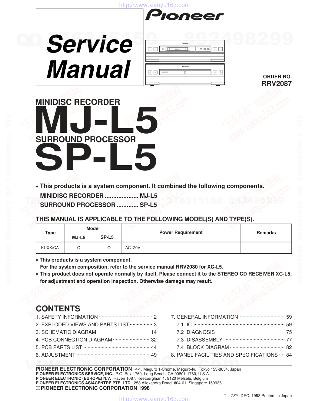
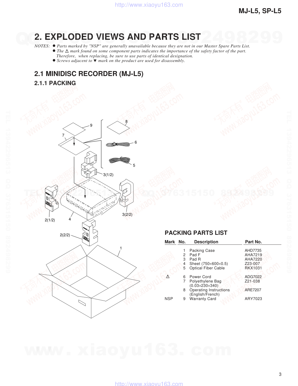
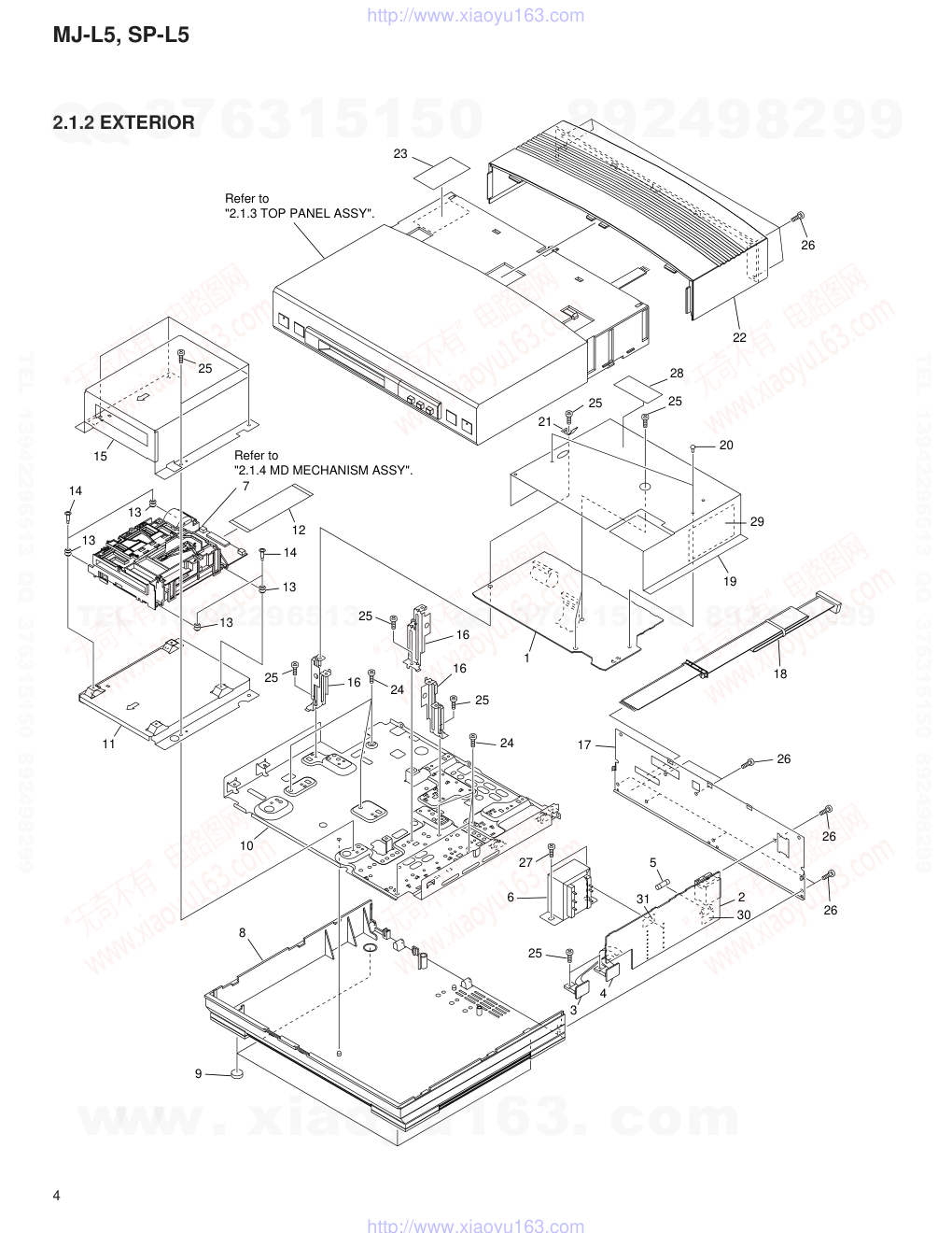
先锋PIONEER MJ-L5音响电路图
 "先锋PIONEER MJ-L5音响电路图-0")
 "先锋PIONEER MJ-L5音响电路图-1")
 "先锋PIONEER MJ-L5音响电路图-2")
 "先锋PIONEER MJ-L5音响电路图-3")
 "先锋PIONEER MJ-L5音响电路图-4")
 "先锋PIONEER MJ-L5音响电路图-5")
 "先锋PIONEER MJ-L5音响电路图-6")
 "先锋PIONEER MJ-L5音响电路图-7")
 "先锋PIONEER MJ-L5音响电路图-8")
 "先锋PIONEER MJ-L5音响电路图-9")
ORDER NO. PIONEER ELECTRONIC CORPORATION 4-1, Meguro 1-Chome, Meguro-ku, Tokyo 153-8654, Japan PIONEER ELECTRONICS SERVICE, INC. P.O. Box 1760, Long Beach, CA 90801-1760, U.S.A. PIONEER ELECTRONIC (EUROPE) N.V. Haven 1087, Keetberglaan 1, 9120 Melsele, Belgium PIONEER ELECTRONICS ASIACENTRE PTE. LTD. 253 Allexandra Road, #04-01, Singapore 159936 � � � � � � � � � �PIONEER ELECTRONIC CORPORATION 1998 c RRV2087 MJ-L5 1. SAFETY INFORMATION ...................................... 2 2. EXPLODED VIEWS AND PARTS LIST ................ 3 3. SCHEMATIC DIAGRAM ..................................... 14 4. PCB CONNECTION DIAGRAM .......................... 32 5. PCB PARTS LIST ............................................... 44 6. ADJUSTMENT .................................................... 49 CONTENTS 7. GENERAL INFORMATION ................................ 59 7.1 IC ................................................................. 59 7.2 DIAGNOSIS ................................................. 75 7.3 DISASSEMBLY ........................................... 77 7.4 BLOCK DIAGRAM ....................................... 82 8. PANEL FACILITIES AND SPECIFICATIONS .... 84 T – ZZY DEC. 1998 Printed in Japan SP-L5 THIS MANUAL IS APPLICABLE TO THE FOLLOWING MODEL(S) AND TYPE(S). SURROUND PROCESSOR • This products is a system component. It combined the following components. MINIDISC RECORDER .................... MJ-L5 SURROUND PROCESSOR ............. SP-L5 • This products is a system component. For the system composition, refer to the service manual RRV2080 for XC-L5. • This product does not operate normally by itself. Please connect it to the STEREO CD RECEIVER XC-L5, for adjustment and operation inspection. Otherwise damage may result. DELAY TIME SFC MODE MODE SFC ON/OFF Ÿ� Ÿ� DOLBY SURROUND P R O • L O G I C MINIDISC ASES 7 0 ¶� 6 ¢� 4 ¡• + – • 1 MINIDISC RECORDER Model MJ-L5 SP-L5 Type Power Requirement Remarks KUXK/CA O O AC120V www. xiaoyu163. com QQ 376315150 9 9 2 8 9 4 2 9 8 TEL 13942296513 9 9 2 8 9 4 2 9 8 0 5 1 5 1 3 6 7 3 Q Q TEL 13942296513 QQ 376315150 892498299 TEL 13942296513 QQ 376315150 892498299 http://www.xiaoyu163.com MJ-L5, SP-L5 2 1. SAFETY INFORMATION This service manual is intended for qualified service technicians; it is not meant for the casual do-it-yourselfer. Qualified technicians have the necessary test equipment and tools, and have been trained to properly and safely repair complex products such as those covered by this manual. Improperly performed repairs can adversely affect the safety and reliability of the product and may void the warranty. If you are not qualified to perform the repair of this product properly and safely, you should not risk trying to do so and refer the repair to a qualified service technician. WARNING This product contains lead in solder and certain electrical parts contain chemicals which are known to the state of California to cause cancer, birth defects or other reproductive harm. Health & Safety Code Section 25249.6 – Proposition 65 1. SAFETY PRECAUTIONS The following check should be performed for the continued protection of the customer and service technician. ANY MEASUREMENTS NOT WITHIN THE LIMITS OUTLINED ABOVE ARE INDICATIVE OF A PO- TENTIAL SHOCK HAZARD AND MUST BE COR- RECTED BEFORE RETURNING THE APPLIANCE TO THE CUSTOMER. 2. PRODUCT SAFETY NOTICE Many electrical and mechanical parts in the appli- ance have special safety related characteristics. These are often not evident from visual inspection nor the protection afforded by them necessarily can be ob- tained by using replacement components rated for voltage, wattage , etc. Replacement parts which have these special safety characteristics are identified in this Service Manual. Electrical components having such features are identified by marking with a on the schematics and on the parts list in this Service Manual. The use of a substitute replacement component which does not have the same safety characteristics as the PIONEER recommended replacement one, shown in the parts list in this Service Manual, may create shock, fire, or other hazards. Product Safety is continuously under review and new instructions are issued from time to time. For the latest information, always consult the current PIONEER Service Manual. A subscription to, or ad- ditional copies of, PIONEER Service Manual may be obtained at a nominal charge from PIONEER. LEAKAGE CURRENT CHECK Measure leakage current to a known earth ground (water pipe, conduit, etc.) by connecting a leakage current tester such as Simpson Model 229-2 or equivalent between the earth ground and all exposed metal parts of the appliance (input/output terminals, screwheads, metal overlays, control shaft, etc.). Plug the AC line cord of the appliance directly into a 120V AC 60 Hz outlet and turn the AC power switch on. Any current measured must not exceed 3.5 mA. (FOR USA MODEL ONLY) Also test with plug reversed (Using AC adapter plug as required) Device under test Test all exposed metal surfaces Earth ground Leakage current tester Reading should not be above 3.5 mA AC Leakage Test REMARQUE (POUR MODÈLE CANADIEN SEULEMENT) Les symboles de fusible (fusible de type rapide) et/ou (fusible de type lent) sur CCI indiquent que les pièces de remplacement doivent avoir la même désignation. NOTICE (FOR CANADIAN MODEL ONLY) Fuse symbols (fast operating fuse) and/or (slow operating fuse) on PCB indicate that replacement parts must be of identical designation. IMPORTANT THIS PIONEER APPARATUS CONTAINS LASER OF CLASS 1. SERVICING OPERATION OF THE APPARATUS SHOULD BE DONE BY A SPECIALLY INSTRUTED PERSON. LASER DIODE CHARACTERISTICS MAXIMUM OUTPUT POWER: 32 mw WAVELENGTH: 785 nm www. xiaoyu163. com QQ 376315150 9 9 2 8 9 4 2 9 8 TEL 13942296513 9 9 2 8 9 4 2 9 8 0 5 1 5 1 3 6 7 3 Q Q TEL 13942296513 QQ 376315150 892498299 TEL 13942296513 QQ 376315150 892498299 http://www.xiaoyu163.com 3 MJ-L5, SP-L5 1 2(1/2) 3(1/2) 3(2/2) 4 7 9 8 6 5 2(2/2) 2.1 MINIDISC RECORDER (MJ-L5) 2.1.1 PACKING PACKING PARTS LIST Mark No. Description Part No. 2. EXPLODED VIEWS AND PARTS LIST NOTES: • Parts marked by "NSP" are generally unavailable because they are not in our Master Spare Parts List. • The mark found on some component parts indicates the importance of the safety factor of the part. Therefore, when replacing, be sure to use parts of identical designation. • Screws adjacent to mark on the product are used for disassembly. 1 Packing Case AHD7735 2 Pad F AHA7219 3 Pad R AHA7220 4 Sheet (750×600×0.5) Z23-007 5 Optical Fiber Cable RKX1031 6 Power Cord ADG7022 7 Polyethylene Bag Z21-038 (0.03×230×340) 8 Operating Instructions ARE7207 (English/French) NSP 9 Warranty Card ARY7023 www. xiaoyu163. com QQ 376315150 9 9 2 8 9 4 2 9 8 TEL 13942296513 9 9 2 8 9 4 2 9 8 0 5 1 5 1 3 6 7 3 Q Q TEL 13942296513 QQ 376315150 892498299 TEL 13942296513 QQ 376315150 892498299 http://www.xiaoyu163.com 4 MJ-L5, SP-L5 Refer to "2.1.3 TOP PANEL ASSY". 25 15 14 14 13 13 13 11 10 8 9 25 16 13 12 25 21 25 24 24 27 6 25 5 2 26 26 26 17 18 3 4 1 25 16 19 25 20 16 7 Refer to "2.1.4 MD MECHANISM ASSY". 23 22 26 31 30 28 29 2.1.2 EXTERIOR www. xiaoyu163. com QQ 376315150 9 9 2 8 9 4 2 9 8 TEL 13942296513 9 9 2 8 9 4 2 9 8 0 5 1 5 1 3 6 7 3 Q Q TEL 13942296513 QQ 376315150 892498299 TEL 13942296513 QQ 376315150 892498299 http://www.xiaoyu163.com 5 MJ-L5, SP-L5 EXTERIOR PARTS LIST Mark No. Description Part No. 1 MD MAIN Unit AWU7125 2 MD TRANS Unit AWU7126 3 MD REG1 Unit AWU7154 4 MD REG2 Unit AWU7155 5 Fuse (FU1 : 400mA/125V) VEK1008 6 Power Transformer (T1) ATT7036 NSP 7 MD MECHANISM Assy AXA7069 8 Bottom Base AMA7006 9 Leg AEB7090 NSP 10 Bottom Plate ANF7010 11 MD Base ANG7191 12 30P F•F•C/30V ADD7097 13 Float Rubber REB1328 14 Float Screw RBA1133 15 MD Shield ANG7192 Mark No. Description Part No. 16 Angle ANG7189 17 Rear Panel ANC7802 18 Cord With Plug (J1) ADE7026 19 Shield Barrier AEC7164 20 Rivet VEC1178 21 Earth Plate ANG7168 22 Bonnet AMA7007 23 •••••••• 24 Screw BPZ30P060FZK 25 Screw BBZ30P060FMC 26 Screw VPZ30P080FZK 27 Screw BBZ40P060FMC 28 65 Label ARW7050 29 Barrier MD AEC7184 NSP 30 Fuse Card AAX7691 NSP 31 Fuse Caution B AAX7699 www. xiaoyu163. com QQ 376315150 9 9 2 8 9 4 2 9 8 TEL 13942296513 9 9 2 8 9 4 2 9 8 0 5 1 5 1 3 6 7 3 Q Q TEL 13942296513 QQ 376315150 892498299 TEL 13942296513 QQ 376315150 892498299 http://www.xiaoyu163.com 6 MJ-L5, SP-L5 9 12 8(1/2) 8(2/2) 2 7 5 6 4 3 10 1 11 12 12 2.1.3 TOP PANEL ASSY • TOP PANEL ASSY PARTS LIST Mark No. Description Part No. 1 MD KEYR Unit AWU7108 2 MD KEYL Unit AWU7109 3 Top Panel AMB7515 4 Sub Panel MD AAP7049 5 MD Flap AAN7186 6 MD Spring ABH7154 7 Flap Plate AAT7003 8 Button X Assy AWL7034 9 Sub Panel AAP7058 NSP 10 Top Plate ANK7042 11 Rivet VEC1178 12 Screw VPZ30P080FZK www. xiaoyu163. com QQ 376315150 9 9 2 8 9 4 2 9 8 TEL 13942296513 9 9 2 8 9 4 2 9 8 0 5 1 5 1 3 6 7 3 Q Q TEL 13942296513 QQ 376315150 892498299 TEL 13942296513 QQ 376315150 892498299 http://www.xiaoyu163.com 7 MJ-L5, SP-L5 2.1.4 MD MECHANISM ASSY 49 48 40 22 42 38 43 40 33 44 31 28 32 34 40 11 5 10 17 7 6 4 9 37 19 21 20 18 37 16 26 15 13 14 37 12 53 52 51 A E E F F G G H A B B C C D D 37 8 40 24 25 39 27 41 35 36 29 39 46 23 30 45 2 3 50 47 37 CN103 CN101 CN102 CN105 1 H www. xiaoyu163. com QQ 376315150 9 9 2 8 9 4 2 9 8 TEL 13942296513 9 9 2 8 9 4 2 9 8 0 5 1 5 1 3 6 7 3 Q Q TEL 13942296513 QQ 376315150 892498299 TEL 13942296513 QQ 376315150 892498299 http://www.xiaoyu163.com 8 MJ-L5, SP-L5 • MD MECHANISM ASSY PARTS LIST Mark No. Description Part No. 1 MD CORE MAIN Unit RWZ4326 2 MD CORE SW Unit RWZ4272 3 Lead Card 7P RDD1399 4 Lead Wire RKP1814 5 Lever Spring RBH1463 6 Clamp Spring 1 RBK1074 7 Clamp Spring 2 RBK1075 8 Loading Belt REB1329 9 Lock Plate RNE1949 10 Loading Base RNK2312 11 Under Slider RNK2314 12 Gear Pulley RNK2316 13 Drive Gear RNK2317 14 Clutch Gear RNK2318 15 Flip Disk RNK2319 16 SW Lever RNK2320 17 Shutter Assy RXA1774 NSP 18 Upper Slider Assy RXA1775 19 Eject Spring RBH1461 20 Upper Slider RNK2313 21 Carrier RNK2315 22 Screw RBA1129 23 Spindle Spring RBH1460 24 Lifter SP RBH1462 25 Screw Guide RBK1072 26 S. H. Spring RBK1073 27 Guide Shaft RLA1312 28 Lead Screw RLA1311 29 Shield Case RNE1950 30 Reference Plate RNK2306 31 S. Holder RNK2307 32 Worm Wheel RNK2309 33 Hook RNK2310 34 Head Lifter RNK2311 35 MD Head RPB1062 36 MD Pickup RWY1018 37 Screw IPZ20P080FMC 38 Screw JFZ17P020FZK 39 Screw JGZ14P020FMC 40 Screw JGZ17P030FMC 41 Screw JGZ17P040FZK 42 Screw PMB20P040FMC 43 Servo Base Assy REA1283 NSP 44 Clamp Magnet RMF1002 NSP 45 Servo Base RNE1946 NSP 46 Disc Table RNK2305 NSP 47 Spindle Motor RXM1091 48 Carriage Motor Assy REA1284 49 Worm RNK2308 NSP 50 Carriage Motor RXM1090 51 Loading Motor Assy REA1285 52 DC Motor /0.75W PXM1010 53 CA Pulley (1) VNL1197 Mark No. Description Part No. www. xiaoyu163. com QQ 376315150 9 9 2 8 9 4 2 9 8 TEL 13942296513 9 9 2 8 9 4 2 9 8 0 5 1 5 1 3 6 7 3 Q Q TEL 13942296513 QQ 376315150 892498299 TEL 13942296513 QQ 376315150 892498299 http://www.xiaoyu163.com 9 MJ-L5, SP-L5 8 6 1 2(1/2) 3(1/2) 3(2/2) 4 7 10 9 11 5 2(2/2) 2.2 SURROUND PROCESSOR (SP-L5) 2.2.1 PACKING PACKING PARTS LIST Mark No. Description Part No. 1 Packing Case AHD7736 2 Pad F AHA7219 3 Pad R AHA7220 4 Sheet (750×600×0.5) Z23-007 5 Remote Control Unit AXD7171 (CU-SP005) 6 Power Cord ADG7022 7 Polyethylene Bag Z21-038 (0.03×230×340) 8 Operating Instructions ARE7206 (English/French) 9 Battery Cover AZA7050 NSP 10 Warranty Card ARY7023 NSP 11 Dry Cell Battery (R03,AAA) VEM1018 www. xiaoyu163. com QQ 376315150 9 9 2 8 9 4 2 9 8 TEL 13942296513 9 9 2 8 9 4 2 9 8 0 5 1 5 1 3 6 7 3 Q Q TEL 13942296513 QQ 376315150 892498299 TEL 13942296513 QQ 376315150 892498299 http://www.xiaoyu163.com 10 MJ-L5, SP-L5 Refer to "2.2.3 TOP PANEL ASSY". 17 16 21 21 20 10 8 27 19 22 20 20 23 7 15 24 13 24 24 4 5 3 2 21 12 6 21 21 21 11 1 25 9 18 24 30 30 26 28 24 14 29 2.2.2 EXTERIOR www. xiaoyu163. com QQ 376315150 9 9 2 8 9 4 2 9 8 TEL 13942296513 9 9 2 8 9 4 2 9 8 0 5 1 5 1 3 6 7 3 Q Q TEL 13942296513 QQ 376315150 892498299 TEL 13942296513 QQ 376315150 892498299 http://www.xiaoyu163.com 11 MJ-L5, SP-L5 (1) EXTERIOR PARTS LIST Mark No. Description Part No. Mark No. Description Part No. 1 PRO MAIN Unit AWU7122 2 PRO AMP Unit AWU7102 3 PRO TRANS Unit AWU7124 4 PRO AUX Unit AWU7146 5 Fuse (FU1 : 1.6A/125V) REK1077 6 Power Transformer (T) ATS7239 NSP 7 Heat Sink ANH7107 8 Bottom Base AMA7009 9 Leg AEB7090 NSP 10 Bottom Plate ANF7010 11 Angle ANG7189 12 Cord Clamper RNH-184 13 Rear Panel ANC7803 14 Rear Case AMR7207 15 Cord With Plug ADE7026 16 Top Barrier AEC7151 17 Rivet VEC1178 18 Bonnet AMA7007 19 Name Label ARW7047 20 Screw BPZ30P060FZK 21 Screw BBZ30P060FMC 22 Screw BBZ40P060FMC 23 Screw BBZ30P140FMC 24 Screw VPZ30P080FZK 25 65 Label ARW7050 26 DC Fan Motor AXM7003 27 Front Leg AEB7102 28 F Cushion AEB7127 29 Cussion Rubber AEB7068 30 Screw BPZ30P300FMC www. xiaoyu163. com QQ 376315150 9 9 2 8 9 4 2 9 8 TEL 13942296513 9 9 2 8 9 4 2 9 8 0 5 1 5 1 3 6 7 3 Q Q TEL 13942296513 QQ 376315150 892498299 TEL 13942296513 QQ 376315150 892498299 http://www.xiaoyu163.com 12 MJ-L5, SP-L5 5 6 7 8 3 11 10 4 1 2 9(3/3) 9(2/3) 9(1/3) 11 11 12 2.2.3 TOP PANEL ASSY • TOP PANEL ASSY PARTS LIST Mark No. Description Part No. 1 PRO KEYR Unit AWU7104 2 PRO KEYL Unit AWU7105 3 PRO IND Unit AWU7145 4 Top Panel AMB7516 5 Sub Panel PR AAP7050 6 Lens D AAX7640 7 Illumination Filter VEC1950 8 Illumination Holder VNK4098 9 Button X Assy AWL7035 NSP 10 Top Plate ANK7048 11 Screw VPZ30P080FZK 12 Rivet VEC1178 www. xiaoyu163. com QQ 376315150 9 9 2 8 9 4 2 9 8 TEL 13942296513 9 9 2 8 9 4 2 9 8 0 5 1 5 1 3 6 7 3 Q Q TEL 13942296513 QQ 376315150 892498299 TEL 13942296513 QQ 376315150 892498299 http://www.xiaoyu163.com 13 MJ-L5, SP-L5 www. xiaoyu163. com QQ 376315150 9 9 2 8 9 4 2 9 8 TEL 13942296513 9 9 2 8 9 4 2 9 8 0 5 1 5 1 3 6 7 3 Q Q TEL 13942296513 QQ 376315150 892498299 TEL 13942296513 QQ 376315150 892498299 http://www.xiaoyu163.com MJ-L5, SP-L5 14 A B C D 1 2 3 4 1 2 3 4 3. SCHEMATIC DIAGRAM 3.1 MINIDISC RECORDER (MJ-L5) 3.1.1 OVERALL CONNECTION DIAGRAM MD MAIN UNIT (AWU7125) MD TRANS UNIT (AWU7126) D MD REG2 UNIT (AWU7155) MD REG1 UNIT (AWU7154) E F MD KEYR UNIT (AWU7108) G MD KEYL UNIT (AWU7109) H C C 1/2 - C 2/2 ( ) AC POWER CORD ADG7022 AC120V VEK1008 (400mA/125V) Power Transformer ATT7036 (1A /125V) AKP7032 (2.5A/250V 7A/125V) www. xiaoyu163. com QQ 376315150 9 9 2 8 9 4 2 9 8 TEL 13942296513 9 9 2 8 9 4 2 9 8 0 5 1 5 1 3 6 7 3 Q Q TEL 13942296513 QQ 376315150 892498299 TEL 13942296513 QQ 376315150 892498299 http://www.xiaoyu163.com MJ-L5, SP-L5 15 A B C D 5 6 7 8 5 6 7 8 MD MECHANISM ASSY (AXA7069) MD CORE MAIN UNIT (RWZ4326) A MD CORE SW UNIT (RWZ4272) B CN104 RKN1039 NON-CONNECTION STEREO CD RECEIVER (XC-L5) or SURROUND PROCESSOR (SP-L5) INTERFACE IC4240 (BU4066BCF) JA4601 GP1F32R IC4171 (TC74HCT08AF) REC AMP IC4202 (NJM4558MD) BUFFER ALC IC4201 (NJM4558MD) BUFFER IC4250 (NJM4558MD) AD/DA CONVERTER OUTPUT SEL. IC4301 (AK4520A) Q4203 (630mA/125V) (500mA/125V) Note : When ordering service parts, be sure to refer to "EXPLODED VIEWS and PARTS LIST" or "PCB PARTS LIST". www. xiaoyu163. com QQ 376315150 9 9 2 8 9 4 2 9 8 TEL 13942296513 9 9 2 8 9 4 2 9 8 0 5 1 5 1 3 6 7 3 Q Q TEL 13942296513 QQ 376315150 892498299 TEL 13942296513 QQ 376315150 892498299 http://www.xiaoyu163.com MJ-L5, SP-L5 16 A B C D 1 2 3 4 1 2 3 4 MD CORE MAIN UNIT (RWZ4326) A MD CORE SW UNIT (RWZ4272) B LOADING MOTOR SLED MOTOR SPINDLE MOTOR YELLOW BLACK ORANGE BLUE BLACK RED INSIDE SW A : DISC PROTECT B : DISC MEDIA DETECT PICKUP 1 2 3 10 11 8 9 A B 3.1.2 MD CORE MAIN and MD CORE SW UNITS www. xiaoyu163. com QQ 376315150 9 9 2 8 9 4 2 9 8 TEL 13942296513 9 9 2 8 9 4 2 9 8 0 5 1 5 1 3 6 7 3 Q Q TEL 13942296513 QQ 376315150 892498299 TEL 13942296513 QQ 376315150 892498299 http://www.xiaoyu163.com MJ-L5, SP-L5 17 A B C D 5 6 7 8 5 6 7 8 (INSIDE) C CN4101 1/2 YB 0.01 R291–R293 : 47k : PLAYBACK SIGNAL : REC SIGNAL : OUTPUT DIGITAL AUDIO SIGNAL : INPUT DIGITAL AUDIO SIGNAL : RF SIGNAL SIGNAL ROUTE 6 5 7 4 A A ¶ 1 – - are waveform numbers on pages 24 and 25. www. xiaoyu163. com QQ 376315150 9 9 2 8 9 4 2 9 8 TEL 13942296513 9 9 2 8 9 4 2 9 8 0 5 1 5 1 3 6 7 3 Q Q TEL 13942296513 QQ 376315150 892498299 TEL 13942296513 QQ 376315150 892498299 http://www.xiaoyu163.com MJ-L5, SP-L5 18 A B C D 1 2 3 4 1 2 3 4 C 1/2 3.1.3 MD MAIN (1/2), MD TRANS, MD REG1 and MD REG2 UNITS : C 1/2 MD MAIN UNIT(1/2) (AWU7125) C 2/2 A CN104 4.9 4.9 4.9 4.9 3.2 5 (D) (D) (D) (D) (D) (D) (D) (D) (D) 5 –4.4 4.1 3 www. xiaoyu163. com QQ 376315150 9 9 2 8 9 4 2 9 8 TEL 13942296513 9 9 2 8 9 4 2 9 8 0 5 1 5 1 3 6 7 3 Q Q TEL 13942296513 QQ 376315150 892498299 TEL 13942296513 QQ 376315150 892498299 http://www.xiaoyu163.com MJ-L5, SP-L5 19 A B C D 5 6 7 8 5 6 7 8 C 1/2 D E F POWER TRANSFORMER FU1: VEK1008 MD REG1 UNIT (AWU7154) MD REG2 UNIT (AWU7155) E MD TRANS UNIT (AWU7126) D F CAUTION : FOR CONTINUED PROTECTION AGAINST RISK OF FIRE. REPLACE WITH SAME TYPE NO. 491.630 MFD. BY LITTELFUSE INC. FOR IC4013(AEK7006). CAUTION : FOR CONTINUED PROTECTION AGAINST RISK OF FIRE. REPLACE WITH SAME TYPE NO. 491.500 MFD. BY LITTELFUSE INC. FOR IC4014(AEK7005). CAUTION : FOR CONTINUED PROTECTION AGAINST RISK OF FIRE. REPLACE WITH SAME TYPE NO. 491001 MFD. BY LITTELFUSE INC. FOR IC4052(AEK7009). NON-CONNECTION STEREO CD RECEIVER (XC-L5) or SURROUND PROCESSOR (SP-L5) 4.9 –4.4 4.9 4.9 5 5 13.3 : PLAYBACK SIGNAL ROUTE : RECORDING SIGNAL ROUTE : DIGITAL AUDIO SIGNAL ROUTE (D) AKP7032 (400mA/125V) ATT7036 www. xiaoyu163. com QQ 376315150 9 9 2 8 9 4 2 9 8 TEL 13942296513 9 9 2 8 9 4 2 9 8 0 5 1 5 1 3 6 7 3 Q Q TEL 13942296513 QQ 376315150 892498299 TEL 13942296513 QQ 376315150 892498299 http://www.xiaoyu163.com MJ-L5, SP-L5 20 A B C D 1 2 3 4 1 2 3 4 C 2/2 G H 3.1.4 MD MAIN (2/2) , MD KEYR and MD KEYL UNITS C 2/2 MD MAIN UNIT (2/2) (AWU7125) MD KEYL UNIT (AWU7109) H MD KEYR UNIT (AWU7108) G www. xiaoyu163. com QQ 376315150 9 9 2 8 9 4 2 9 8 TEL 13942296513 9 9 2 8 9 4 2 9 8 0 5 1 5 1 3 6 7 3 Q Q TEL 13942296513 QQ 376315150 892498299 TEL 13942296513 QQ 376315150 892498299 http://www.xiaoyu163.com MJ-L5, SP-L5 21 A B C D 5 6 7 8 5 6 7 8 C 2/2 C 1/2 C 1/2 www. xiaoyu163. com QQ 376315150 9 9 2 8 9 4 2 9 8 TEL 13942296513 9 9 2 8 9 4 2 9 8 0 5 1 5 1 3 6 7 3 Q Q TEL 13942296513 QQ 376315150 892498299 TEL 13942296513 QQ 376315150 892498299 http://www.xiaoyu163.com MJ-L5, SP-L5 22 1.53V 3.18V 1.65V 0V 1.42V 0V 1.59V 1.41V 1.97V 1.39V 1.64V 3.18V 0V 0V 0V 0V 1.69V 1.52V 1.70V 1.47V 1.47V 1.65V 1.54V 1.69V 1.51V 0.82V 2.0V 2.0V 1.81V 1.4V 0.82V 1.67V 1.67V 1.67V 2.86V 1.32V 2.23V 0V 2.4V 1.2V 1.5V 0V 2.0V 3.0V 1.2V 1.2V 0.02V 3.04V 1.57V 0.05V 9 8 7 6 5 4 3 2 1 30 29 28 27 26 25 24 23 22 21 20 19 18 17 16 15 14 13 12 11 10 49 48 47 46 45 44 43 42 41 40 39 38 37 36 35 34 33 32 31 PIN NO. VOLTAGE 50 IC102 1.59V 0V 0V 1.59V 1.8V 0V 0V 0V 0V 0V 0.56V 3.18V 0V 1.5V 1.5V 3.2V 1.6V 3.2V 0V 1.6V 1.6V 1.48V 0V 0V 1.68V 1.82V 1.59V 0.35V 0.02V 3.2V 3.2V 0.02V 0.03V 1.9V 1.56V 3.1V 3.2V 0V 3.19V 0.5V 0.5V 0.5V 0.5V 0.9V 0.5V 0.5V 0.5V 0.8V 3.18V 0.06V 59 58 57 56 55 54 53 52 51 79 78 77 76 75 74 73 72 71 70 69 68 67 66 65 64 63 62 61 60 98 97 96 95 94 93 92 91 90 89 88 87 86 85 84 83 82 81 80 PIN NO. VOLTAGE 99 100 0V 0V 0.22V 0.03V 1.29V 2.21V 3.13V 0V 0V 0V 0V 3.03V 1.43V 0V 1.57V 3.2V 3.19V 3.1V 0.03V 0V 0V 3.18V 3.2V 0V 2.67V 3.19V 0V 0V 2.4V 0.24V 0V 0.3V 3.2V 1.56V 1.0V 0V 2.77V 0V 3.18V 0.02V 3.19V 3.2V 0V 0.05V 3.18V 3.19V 0.51V 0.4V 0.3V 0.55V 9 8 7 6 5 4 3 2 1 30 29 28 27 26 25 24 23 22 21 20 19 18 17 16 15 14 13 12 11 10 49 48 47 46 45 44 43 42 41 40 39 38 37 36 35 34 33 32 31 PIN NO. VOLTAGE 50 IC104 0.54V 0.6V 0.6V 0.6V 0V 0V 0V 0V 3.2V 0V 0V 3.2V 0V 0V 3.2V 0V 0V 0V 0V 0V 0V 3.1V 3.2V 0V 0V 3.2V 0V 0V 0V 3.2V 0V 3.19V 0V 3.19V 0V 3.18V 3.2V 0V 1.03V 1.6V 0.56V 1.49V 1.49V 0.68V 0.61V 0V 0.53V 3.2V 3.2V 0V 59 58 57 56 55 54 53 52 51 79 78 77 76 75 74 73 72 71 70 69 68 67 66 65 64 63 62 61 60 98 97 96 95 94 93 92 91 90 89 88 87 86 85 84 83 82 81 80 PIN NO. VOLTAGE 99 100 0.78V 0.73V 0.77V 0.75V 1.61V 1.61V 0.75V 1.61V 1.61V 1.61V 1.61V 1.61V 3.19V 3.19V 0V 0V 3.19V 0V 0V 1.5V 3.2V 0V 0V 3.19V 2.0V 0V 1.40V 1.42V 1.40V 1.63V 1.61V 1.61V 0V 0V 0V 1.62V 0.59V 1.61V 1.61V 1.61V 1.61V 3.19V 0V 1.08V 1.61V 1.61V 0V 0.74V 9 8 7 6 5 4 3 2 1 30 29 28 27 26 25 24 23 22 21 20 19 18 17 16 15 14 13 12 11 10 42 43 44 45 46 47 48 41 40 39 38 37 36 35 34 33 32 31 VOLTAGE IC101 PIN NO. 1.2V 1.2V 3.0V 2.0V 0V 2.23V 1.32V 2.86V 1.67V 3.18V 1.67V 1.67V 1.67V 2.86V 1.32V 2.23V 2.4V 1.2V 1.5V 0V 9 5 4 3 2 1 26 25 24 23 22 18 17 16 15 14 13 12 11 10 PIN NO. VOLTAGE IC103 Voltages MD CORE MAIN UNIT A www. xiaoyu163. com QQ 376315150 9 9 2 8 9 4 2 9 8 TEL 13942296513 9 9 2 8 9 4 2 9 8 0 5 1 5 1 3 6 7 3 Q Q TEL 13942296513 QQ 376315150 892498299 TEL 13942296513 QQ 376315150 892498299 http://www.xiaoyu163.com MJ-L5, SP-L5 23 9 8 7 6 5 4 3 2 1 16 15 14 13 12 11 10 PIN NO. VOLTAGE IC108 2.47V 2.63V 4.87V 2.63V 1.59V 0V 0V 4.87V 0V 2.25V 4.94V 4.94V 4.94V 4.94V 3.12V 4.94V 9 8 7 6 5 4 3 2 1 14 13 12 11 10 PIN NO. VOLTAGE IC109 2.77V 2.77V 3.2V 1.58V 1.58V 1.56V 0V 0V 0V 0V 0V 0V 0V 3.2V 9 8 7 6 5 4 3 2 1 20 19 18 17 16 15 14 13 12 11 10 PIN NO. VOLTAGE IC116 4.98V 0V 0V 4.99V 3.2V 0V 0.03V 3.18V 0V 0V 0V 0.22V 0V 0.25V 0.25V 2.82V 0.16V 4.94V 2.82V 1.33V 1.6V 0.49V 1.61V 4.99V 4.99V 1.61V 1.62V 2.46V 2.51V 0V 0V 2.54V 2.45V 1.62V 1.62V 1.61V 3.17V 0V 1.61V 1.61V 1.61V 1.61V 1.36V 1.36V 1.61V 1.61V 1.63V 2.41V 2.55V 2.47V 2.48V 0V 0V 2.79V 2.18V 0V 1.69V 5.0V 4.99V 1.67V 1.69V 1.69V 9 8 7 6 5 4 3 2 1 30 29 28 27 26 25 24 23 22 21 20 19 18 17 16 15 14 13 12 11 10 42 41 40 39 38 37 36 35 34 33 32 31 VOLTAGE IC106 PIN NO. 1.66V 1.62V 1.62V 0V 1.67V 1.67V 1.67V 3.19V 8 7 6 5 4 3 2 1 PIN NO. VOLTAGE IC112 0V 3.2V 0V 3.2V 0V 0.11V 0V 0V 8 7 6 5 4 3 2 1 PIN NO. VOLTAGE IC110 9 8 7 6 5 4 3 2 1 14 13 12 11 10 PIN NO. VOLTAGE IC113 4.95V 3.96V 0V 0V 0V 0V 0V 0V 4.94V 4.12V 3.19V 0V 0V 4.94V 0V 4.19V 3.21V 2.81V 0V 5 4 3 2 1 PIN NO. VOLTAGE IC114 www. xiaoyu163. com QQ 376315150 9 9 2 8 9 4 2 9 8 TEL 13942296513 9 9 2 8 9 4 2 9 8 0 5 1 5 1 3 6 7 3 Q Q TEL 13942296513 QQ 376315150 892498299 TEL 13942296513 QQ 376315150 892498299 http://www.xiaoyu163.com MJ-L5, SP-L5 24 1 –– GND DC500mV/div., 10 µSec/div. IC101-pin35 (ADIPO) MODE: PLAY DISC: GGF1328 (MMD–212) 2 IC101-pin30 (WBO) MODE: PLAY DISC: GGF1328 (MMD–212) –– GND DC1V/div., 10 µSec/div. 3 IC102-pin1 (EFM MON) MODE: PLAY DISC: TGTS1 or MMD–110 –– GND DC500mV/div., 0.5mSec/div. 6 –– GND DC500mV/div., 2mSec/div. IC102-pin77 (TE MON) MODE: PLAY DISC: TGTS1 or MMD–110 7 IC102-pin54 (TES01) MODE: STOP –– GND DC2V/div., 10 µSec/div. 4 –– GND DC1V/div., 0.2 µSec/div. IC102-pin50 (EFMO) MODE: REC DISC: GGF1328 (MMD–212) 5 IC102-pin75 (FE MON) MODE: PLAY DISC: TGTS1 or MMD–110 –– GND DC100mV/div., 2mSec/div. 39 kΩ 820pF FE MON Note: The encircled numbers denote measuring point in the schematic diagram and the PCB connection diagram. Measurement Method Measurement Method REFO (MD Mechanism Assy TP) To Oscilloscope 39 kΩ 820pF TE MON REFO (MD Mechanism Assy TP) To Oscilloscope Waveforms MD CORE MAIN UNIT A www. xiaoyu163. com QQ 376315150 9 9 2 8 9 4 2 9 8 TEL 13942296513 9 9 2 8 9 4 2 9 8 0 5 1 5 1 3 6 7 3 Q Q TEL 13942296513 QQ 376315150 892498299 TEL 13942296513 QQ 376315150 892498299 http://www.xiaoyu163.com MJ-L5, SP-L5 25 11 –– GND DC1V/div., 1mSec/div. CN105-pin1 (LOAD –) MODE: EJECT 8 –– GND DC500mV/div., 2mSec/div. CN103-pin1 (SLD +) MODE: PLAY 9 CN103-pin4 (SP +) MODE: PLAY –– GND DC500mV/div., 5mSec/div. 10 CN105-pin1 (LOAD –) MODE: STOP –– GND DC1V/div., 1mSec/div. www. xiaoyu163. com QQ 376315150 9 9 2 8 9 4 2 9 8 TEL 13942296513 9 9 2 8 9 4 2 9 8 0 5 1 5 1 3 6 7 3 Q Q TEL 13942296513 QQ 376315150 892498299 TEL 13942296513 QQ 376315150 892498299 http://www.xiaoyu163.com MJ-L5, SP-L5 26 A B C D 1 2 3 4 1 2 3 4 3.2 SURROUND PROCESSOR (SP-L5) 3.2.1 OVERALL CONNECTION DIAGRAM PRO KEYL UNIT (AWU7105) N PRO AMP UNIT (AWU7102) K PRO TRANS UNIT (AWU7124) J PRO KEYR UNIT (AWU7104) L PRO IND UNIT (AWU7145) M IC3401 POWER AMP +10dB AMP FUNC1 DOLBY BUFFER1 REAR & CENTER VOL. IC3201 IC3551 IC3571 IC3701 IC3001 C S C L,R S AC POWER CORD ADG7022 AC120V ATS7239 ATT7027 AKP7032 DC FANMOTOR AXM7003 CN3651 KM200SA2L GND UNREG- REK1077 (1.6A/125V) www. xiaoyu163. com QQ 376315150 9 9 2 8 9 4 2 9 8 TEL 13942296513 9 9 2 8 9 4 2 9 8 0 5 1 5 1 3 6 7 3 Q Q TEL 13942296513 QQ 376315150 892498299 TEL 13942296513 QQ 376315150 892498299 http://www.xiaoyu163.com MJ-L5, SP-L5 27 A B C D 5 6 7 8 5 6 7 8 1/2, 2/2 PRO MAIN UNIT (AWU7122) I PRO AUX UNIT (AWU7146) O I I FUNC2 IC3501 BUFFER2 IC3531 STEREO CD RECEIVER (XC-L5) MINIDISC RECORDER (MJ-L5) SPEAKER www. xiaoyu163. com QQ 376315150 9 9 2 8 9 4 2 9 8 TEL 13942296513 9 9 2 8 9 4 2 9 8 0 5 1 5 1 3 6 7 3 Q Q TEL 13942296513 QQ 376315150 892498299 TEL 13942296513 QQ 376315150 892498299 http://www.xiaoyu163.com MJ-L5, SP-L5 28 A B C D 1 2 3 4 1 2 3 4 1/2 I J 3.2.2 PRO MAIN (1/2), PRO TRANS and PRO AMP UNITS • NOTE FOR FUSE REPLACEMENT FOR CONTINUED PROTECTION AGAINST RISK OF FIRE, REPLACE WITH SAME TYPE AND RATINGS OF FUSE. CAUTION - 1/2 PRO MAIN UNIT (AWU7122) PRO TRANS UNIT (AWU7124) J 2/2 I I CAUTION : FOR CONTINUED PROTECTION AGAINST RISK OF FIRE, REPLACE ONLY WITH SAME TYPE NO. 491001 FOR IC11 AND IC12 NO. 491007 FOR IC21 AND IC22 MFD. BY LITTELFUSE INK. CAUTION : FOR CONTINUED PROTECTION AGAINST RISK OF FIRE. REPLACE ONLY WITH SAME TYPE NO. 49103.5 MFD. BY LITTELFUSE INC. FOR IC3 AND IC4. CAUTION : FOR CONTINUED PROTECTION AGAINST RISK OF FIRE. REPLACE ONLY WITH SAME TYPE NO. 491.315 MFD. BY LITTELFUSE INC. FOR IC1. AKP7032 REK1077 (1.6A/125V) C2 0.01 /250 0.01 /250 H1,H2 : AKR1003 IC11 AEK7009 491001(1A/125V) IC12 AEK7009 491001 (1A/125V) AEK7021 491007(7A/125V) AEK7021 491007(7A/125V) AEK7017 49103.5(3.5A/125V) AEK7017 49103.5(3.5A/125V) ATS7239 Power Transformer POWER TRANSFORMER (STANDBY) AEK7003 491.315(315mA/125V) AC POWER CORD 9.4 –9.4 13.8 12 5 –13.8 27.7 –27.7 –6.8 5.7 W115, W116 www. xiaoyu163. com QQ 376315150 9 9 2 8 9 4 2 9 8 TEL 13942296513 9 9 2 8 9 4 2 9 8 0 5 1 5 1 3 6 7 3 Q Q TEL 13942296513 QQ 376315150 892498299 TEL 13942296513 QQ 376315150 892498299 http://www.xiaoyu163.com MJ-L5, SP-L5 29 A B C D 5 6 7 8 5 6 7 8 1/2 I K PRO AMP UNIT (AWU7102) 2/2 : C CH AUDIO SIGNAL ROUTE : S CH AUDIO SIGNAL ROUTE K I AKE7042 L3461,L3462 : ATH-059 R3461 100 R3462 100 R3617,R3618 : ACN7032 IC3201(1/2) IC3201(2/2) SPEAKER –26.5 26.5 –25.3 POWER AMP DC FANMOTOR www. xiaoyu163. com QQ 376315150 9 9 2 8 9 4 2 9 8 TEL 13942296513 9 9 2 8 9 4 2 9 8 0 5 1 5 1 3 6 7 3 Q Q TEL 13942296513 QQ 376315150 892498299 TEL 13942296513 QQ 376315150 892498299 http://www.xiaoyu163.com MJ-L5, SP-L5 30 A B C D 1 2 3 4 1 2 3 4 2/2 I L M N 3.2.3 PRO MAIN (2/2), PRO KEYR, PRO IND, PRO KEYL and PRO AUX UNITS PRO KEYR UNIT (AWU7104) L PRO KEYL UNIT (AWU7105) N PRO IND UNIT (AWU7145) M 1/2 I 1/2 I S5901,S5902 : RSG1031 S5921,S5922 : RSG1030 IC5501 PDC046A AC PULSE 5 9.3 PRO KEYR UNIT S5901 : SFC ON/OFF S5902 : SFC MODE PRO KEYL UNIT S5921 : DELAY TIME S5922 : DOLBY MODE www. xiaoyu163. com QQ 376315150 9 9 2 8 9 4 2 9 8 TEL 13942296513 9 9 2 8 9 4 2 9 8 0 5 1 5 1 3 6 7 3 Q Q TEL 13942296513 QQ 376315150 892498299 TEL 13942296513 QQ 376315150 892498299 http://www.xiaoyu163.com MJ-L5, SP-L5 31 A B C D 5 6 7 8 5 6 7 8 2/2 I O 2/2 PRO MAIN UNIT (AWU7122) PRO AUX UNIT (AWU7146) : L CH AUDIO SIGNAL ROUTE : C CH AUDIO SIGNAL ROUTE : S CH AUDIO SIGNAL ROUTE O 1/2 I I (REC) (REC) (REC) (VCR) (REC) (REC) (VCR) (DVD) (DVD) (DVD) (DVD) (VCR) (DVD) (VCR) (DVD) (VCR) (VCR) (REC) (PB) (PB) (PB) (PB) (REC) (REC) (PB) (REC) (REC) IC3571(1/2) NJM4558MD IC3531(1/2) NJM4558MD IC3531(2/2) NJM4558MD IC3571(2/2) NJM4558MD D5201–D5204 : UDZ15B STEREO CD RECEIVER (XC-L5) MINIDISC RECORDER (MJ-L5) www. xiaoyu163. com QQ 376315150 9 9 2 8 9 4 2 9 8 TEL 13942296513 9 9 2 8 9 4 2 9 8 0 5 1 5 1 3 6 7 3 Q Q TEL 13942296513 QQ 376315150 892498299 TEL 13942296513 QQ 376315150 892498299 http://www.xiaoyu163.com MJ-L5, SP-L5 32 A B C D 1 2 3 4 1 2 3 4 NOTE FOR PCB DIAGRAMS : 1. Part numbers in PCB diagrams match those in the schematic diagrams. 2. A comparison between the main parts of PCB and schematic diagrams is shown below. 3. The parts mounted on this PCB include all necessary parts for several destinations. For further information for respective destinations, be sure to check with the schematic diagram. 4. View point of PCB diagrams. Symbol In PCB Diagrams Symbol In Schematic Diagrams Part Name B C E D D G G S S B C E B C E D G S B C E B C E B C E Transistor Transistor with resistor Field effect transistor Resistor array 3-terminal regulator Capacitor Connector P.C.Board Chip Part SIDE A SIDE B B SIDE A SIDE B 4. PCB CONNECTION DIAGRAM 4.1 MINIDISC RECORDER (MJ-L5) 4.1.1 MD CORE SW UNIT SPINDLE MOTOR SLED MOTOR (RNP1721-B) CN103 A MD CORE SW UNIT B www. xiaoyu163. com QQ 376315150 9 9 2 8 9 4 2 9 8 TEL 13942296513 9 9 2 8 9 4 2 9 8 0 5 1 5 1 3 6 7 3 Q Q TEL 13942296513 QQ 376315150 892498299 TEL 13942296513 QQ 376315150 892498299 http://www.xiaoyu163.com MJ-L5, SP-L5 33 A B C D 1 2 3 4 1 2 3 4 LOADING MOTOR REC HEAD PICKUP ASSY IC101 IC112 IC108 IC113 IC109 IC110 IC116 Q103 Q104 IC106 IC102 IC103 IC104 IC114 Q101 Q102 (RNP1721-B) (RNP1721-B) CN701 B CN4101 C MD CORE MAIN UNIT A 1 2 6 7 5 9 8 4 10 11 3 4.1.2 MD CORE MAIN UNIT ¶ 1 – - are waveform numbers on pages 24 and 25. A SIDE A SIDE B www. xiaoyu163. com QQ 376315150 9 9 2 8 9 4 2 9 8 TEL 13942296513 9 9 2 8 9 4 2 9 8 0 5 1 5 1 3 6 7 3 Q Q TEL 13942296513 QQ 376315150 892498299 TEL 13942296513 QQ 376315150 892498299 http://www.xiaoyu163.com MJ-L5, SP-L5 34 A B C D 1 2 3 4 1 2 3 4 CN4011 D J4901 G CN104 A MD MAIN UNIT C (ANP7249-B) IC4183 IC4022 IC4080 IC4025 IC4024 IC4051 IC4013 IC4014 Q4018 Q4020 Q4012 Q4014 STEREO CD RECEIVER (XC-L5) or SURROUND PROCESSOR (SP-L5) C 4.1.3 MD MAIN UNIT SIDE A www. xiaoyu163. com QQ 376315150 9 9 2 8 9 4 2 9 8 TEL 13942296513 9 9 2 8 9 4 2 9 8 0 5 1 5 1 3 6 7 3 Q Q TEL 13942296513 QQ 376315150 892498299 TEL 13942296513 QQ 376315150 892498299 http://www.xiaoyu163.com MJ-L5, SP-L5 35 A B C D 1 2 3 4 1 2 3 4 MD MAIN UNIT C (ANP7249-B) Q4015 | Q4017 Q4101 Q4104 Q4102 Q4243 Q4260 | Q4262 Q4242 Q4241 Q4108 Q4103 Q4022 Q4151 IC4250 IC4101 IC4171 IC4240 IC4301 Q4019 Q4021 Q4040 Q4013 Q4015 Q4201 IC4201 IC4202 Q4016 Q4017 Q4202 | Q4204 Q4230 | Q4232 C SIDE B www. xiaoyu163. com QQ 376315150 9 9 2 8 9 4 2 9 8 TEL 13942296513 9 9 2 8 9 4 2 9 8 0 5 1 5 1 3 6 7 3 Q Q TEL 13942296513 QQ 376315150 892498299 TEL 13942296513 QQ 376315150 892498299 http://www.xiaoyu163.com MJ-L5, SP-L5 36 A B C D 1 2 3 4 1 2 3 4 CN4012 C MD TRANS UNIT D MD KEYL UNIT H MD REG2 UNIT F MD REG1 UNIT E MD KEYR UNIT G AC POWER CORD IC4012 IC4052 IC4011 IC4016 IC4015 CN4102 C (ANP7249-B) 4.1.4 MD TRANS, MD REG1, MD REG2, MD KEYR and MD KEYL UNITS D E F G H SIDE A www. xiaoyu163. com QQ 376315150 9 9 2 8 9 4 2 9 8 TEL 13942296513 9 9 2 8 9 4 2 9 8 0 5 1 5 1 3 6 7 3 Q Q TEL 13942296513 QQ 376315150 892498299 TEL 13942296513 QQ 376315150 892498299 http://www.xiaoyu163.com MJ-L5, SP-L5 37 A B C D 1 2 3 4 1 2 3 4 MD TRANS UNIT D MD KEYL UNIT H MD REG2 UNIT F MD REG1 UNIT E MD KEYR UNIT G (ANP7249-B) D E F G H SIDE B www. xiaoyu163. com QQ 376315150 9 9 2 8 9 4 2 9 8 TEL 13942296513 9 9 2 8 9 4 2 9 8 0 5 1 5 1 3 6 7 3 Q Q TEL 13942296513 QQ 376315150 892498299 TEL 13942296513 QQ 376315150 892498299 http://www.xiaoyu163.com MJ-L5, SP-L5 38 A B C D 1 2 3 4 1 2 3 4 PRO MAIN UNIT I PRO AUX UNIT O MINIDISC RECORDER (MJ-L5) STEREO CD RECEIVER (XC-L5) J5901 L IC21 IC22 IC12 IC11 Q91 I SIDE A 4.2 SURROUND PROCESSOR (SP-L5) 4.2.1 PRO MAIN, PRO AMP and PRO AUX UNITS O www. xiaoyu163. com QQ 376315150 9 9 2 8 9 4 2 9 8 TEL 13942296513 9 9 2 8 9 4 2 9 8 0 5 1 5 1 3 6 7 3 Q Q TEL 13942296513 QQ 376315150 892498299 TEL 13942296513 QQ 376315150 892498299 http://www.xiaoyu163.com MJ-L5, SP-L5 39 A B C D 5 6 7 8 5 6 7 8 PRO AMP UNIT K (ANP7248-C) IC22 IC12 11 Q91 Q52 Q71 Q81 DC FANMOTOR (AXM7003) SIDE A I K www. xiaoyu163. com QQ 376315150 9 9 2 8 9 4 2 9 8 TEL 13942296513 9 9 2 8 9 4 2 9 8 0 5 1 5 1 3 6 7 3 Q Q TEL 13942296513 QQ 376315150 892498299 TEL 13942296513 QQ 376315150 892498299 http://www.xiaoyu163.com MJ-L5, SP-L5 40 A B C D 1 2 3 4 1 2 3 4 SIDE B PRO M I (ANP7248-C) Q3491–Q3494 Q3611–Q3613 Q3601–Q3603 Q3621 Q3651–Q3653 Q53–Q56 IC3201 IC3001 Q3522 Q3521 PRO AMP UNIT K I K www. xiaoyu163. com QQ 376315150 9 9 2 8 9 4 2 9 8 TEL 13942296513 9 9 2 8 9 4 2 9 8 0 5 1 5 1 3 6 7 3 Q Q TEL 13942296513 QQ 376315150 892498299 TEL 13942296513 QQ 376315150 892498299 http://www.xiaoyu163.com MJ-L5, SP-L5 41 A B C D 5 6 7 8 5 6 7 8 PRO MAIN UNIT Q3522 Q3501 Q3502 Q3561 Q3523 IC5501 Q5561 Q5565 Q5571 Q5566–Q5568 Q5562–Q5564 Q3562 IC3531 IC3501 Q3521 IC3571 IC3551 IC3701 PRO AUX UNIT O Q3051–Q3053 SIDE B I O www. xiaoyu163. com QQ 376315150 9 9 2 8 9 4 2 9 8 TEL 13942296513 9 9 2 8 9 4 2 9 8 0 5 1 5 1 3 6 7 3 Q Q TEL 13942296513 QQ 376315150 892498299 TEL 13942296513 QQ 376315150 892498299 http://www.xiaoyu163.com MJ-L5, SP-L5 42 A B C D 1 2 3 4 1 2 3 4 (ANP7248-C) PRO TRANS UNIT J PRO KEYL UNIT N PRO IND UNIT M PRO KEYR UNIT L AC POWER CORD CN11 I CN13 I IC1 IC2 Q1 IC3 IC4 SIDE A 4.2.2 PRO TRANS, PRO KEYR, PRO IND and PRO KEYL UNITS J L M N www. xiaoyu163. com QQ 376315150 9 9 2 8 9 4 2 9 8 TEL 13942296513 9 9 2 8 9 4 2 9 8 0 5 1 5 1 3 6 7 3 Q Q TEL 13942296513 QQ 376315150 892498299 TEL 13942296513 QQ 376315150 892498299 http://www.xiaoyu163.com MJ-L5, SP-L5 43 A B C D 1 2 3 4 1 2 3 4 (ANP7248-C) PRO TRANS UNIT J PRO KEYL UNIT N PRO KEYR UNIT L PRO IND UNIT M SIDE B J L M N www. xiaoyu163. com QQ 376315150 9 9 2 8 9 4 2 9 8 TEL 13942296513 9 9 2 8 9 4 2 9 8 0 5 1 5 1 3 6 7 3 Q Q TEL 13942296513 QQ 376315150 892498299 TEL 13942296513 QQ 376315150 892498299 http://www.xiaoyu163.com 44 MJ-L5, SP-L5 Mark No. Description Part No. Mark No. Description Part No. Mark No. Description Part No. Mark No. Description Part No. 5. PCB PARTS LIST NOTES: •Parts marked by "NSP" are generally unavailable because they are not in our Master Spare Parts List. •The mark found on some component parts indicates the importance of the safety factor of the part. Therefore, when replacing, be sure to use parts of identical designation. •When ordering resistors, first convert resistance values into code form as shown in the following examples. Ex.1 When there are 2 effective digits (any digit apart from 0), such as 560 ohm and 47k ohm (tolerance is shown by J=5%, and K=10%). 560 Ω → 56 × 10 1 → 561 ........................................................ RD1/4PU 5 6 1 J 47k Ω → 47 × 10 3 → 473 ........................................................ RD1/4PU 4 7 3 J 0.5 Ω → R50 ..................................................................................... RN2H R 5 0 K 1 Ω → 1R0 ..................................................................................... RS1P 1 R 0 K Ex.2 When there are 3 effective digits (such as in high precision metal film resistors). 5.62k Ω → 562 × 10 1 → 5621 ...................................................... RN1/4PC 5 6 2 1 F 5.1 MINIDISC RECORDER (MJ-L5) LIST OF ASSEMBLIES MD CORE UNIT RWM2055 MD CORE MAIN UNIT RWZ4326 MD CORE SW UNIT RWZ4272 NSP MDCOMP ASSY AWM7384 MD MAIN UNIT AWU7125 MD TRANS UNIT AWU7126 MD KEYR UNIT AWU7108 MD KEYL UNIT AWU7109 MD REG1 UNIT AWU7154 MD REG2 UNIT AWU7155 MD CORE MAIN UNIT SEMICONDUCTORS IC112 BA4510F IC116 BD7910FV IC110 BR93LC56F IC101 IR3R55M IC102 LR376481 IC106 M56758FP IC103 M5M4V4400CTP-7 IC104 PD5450B IC114 RN5RG32AA IC113 TC74ACT08FT IC109 TC74VHC08FT IC108 TC9246F Q102 2SA1036K Q101 2SB1188 Q103,Q104 DTC124EU D101,D102 SB02-09CP COILS L101,L103,L104,L107 (4.7µH) DTL1024 L110 QTL1015 L108 (47µH) RTL1003 L102 (0.47µH) RTL1007 SWITCHES S101,S102 RSF1012 CAPACITORS C115 CCSQCH101J50 C119,C120 CCSQCH120J50 C146 CCSQCH121J50 C125 CCSQCH150J50 C141-C144,C155 CCSQCH220J50 C174-C178 CCSQCH271J50 C194 CCSQCH331J50 C139 CEV101M4 C131,C166 CEV101M6R3 C147,C148,C201 CEV470M6R3 C112 CEV4R7M35 C193 CKSQYB102K50 C126,C1000 CKSQYB103K50 C153,C154 CKSQYB153K50 C158 CKSQYB222K50 C196-C198 CKSQYB223K50 C103,C145 CKSQYB273K50 C171 CKSQYB332K50 C149,C170 CKSQYB333K50 C106,C159 CKSQYB472K50 C127 CKSQYB474K16 C156,C157 CKSQYB562K50 C151,C152,C160,C162 CKSQYB821K50 C130,C132,C134,C137,C138 CKSQYF104Z25 C161,C163,C164,C173,C195 CKSQYF104Z25 C202-C205 CKSQYF104Z25 C101,C102,C104,C108 CKSQYF105Z16 C113,C114,C116-C118 CKSQYF105Z16 C121,C122,C124,C128 CKSQYF105Z16 C135,C136,C140,C165,C169 CKSQYF105Z16 C207,C208 CKSQYF105Z16 C123 CKSQYF473Z25 C105,C107 CKSQYF474Z16 RESISTORS R105 RS1/8S270J Other Resistors RS1/10S J OTHERS CN104 30P CONNECTOR RKN1039 X101 (33.8688MHz) RSS1055 CN105 ZR CONNECTOR S2B-ZR-SM3A CN102 2P CONNECTOR S2B-ZR-SM3A-R CN101 CONNECTOR SFV28R-1ST CN103 CONNECTOR SFW7R-2ST A www. xiaoyu163. com QQ 376315150 9 9 2 8 9 4 2 9 8 TEL 13942296513 9 9 2 8 9 4 2 9 8 0 5 1 5 1 3 6 7 3 Q Q TEL 13942296513 QQ 376315150 892498299 TEL 13942296513 QQ 376315150 892498299 http://www.xiaoyu163.com 45 MJ-L5, SP-L5 Mark No. Description Part No. Mark No. Description Part No. MD CORE SW UNIT SWITCHES S701 RSF1009 S702 RSF1010 RESISTORS All Resistors RS1/10S J OTHERS CN701 CONNECTOR SFW7R-1ST MD MAIN UNIT SEMICONDUCTORS IC4014 AEK7005 IC4013 AEK7006 IC4301 AK4520A IC4051 BA17805T IC4240 BU4066BCF IC4201,IC4202,IC4250 NJM4558MD IC4101 PDG225A IC4171 TC74HCT08AF Q4017 2PB709A Q4013,Q4015,Q4016,Q4019,Q4021 2PD601A Q4040,Q4151,Q4201-Q4204 2PD601A Q4012,Q4014,Q4020 2SB1237X Q4018 2SD1858X Q4231,Q4232,Q4261,Q4262 2SD2114K Q4022,Q4230,Q4242,Q4260 DTA124EK Q4103 DTC114EK Q4101,Q4102,Q4104-Q4107 DTC114TK Q4241,Q4243 DTC124EK Q4108 DTC143EK D4014 1SR139-400 D4040,D4101,D4151,D4220,D4221 1SS254 D4011 D2SBA20(B) D4703-D4711,D4713,D4714 MTZJ8.2B COILS L4301,L4302,L4601 LAU100J L4101,L4171 LAU220J CAPACITORS C4023 (0.047F/5.5V) ACH1246 C4013 (0.018F/25V) ACH7099 C4157,C4201,C4202,C4211,C4212 CCSQCH101J50 C4314,C4709,C4710 CCSQCH101J50 C4203,C4204 CCSQCH220J50 C4112,C4117,C4118,C4120-C4123 CCSQCH221J50 C4207,C4208 CCSQCH470J50 C4054 CEAL1R0M50 C4022,C4027-C4029,C4034,C4035 CEAT100M50 C4052,C4102,C4205,C4206 CEAT100M50 C4209,C4210,C4213,C4214 CEAT100M50 C4220,C4221,C4241,C4242 CEAT100M50 C4251-C4254 CEAT100M50 C4106,C4215,C4217,C4261,C4263 CEAT101M10 C4302,C4306,C4308,C4603 CEAT101M10 C4014 CEAT221M25 C4222 CEAT330M25 C4026,C4030,C4031,C4036,C4061 CEAT470M16 C4171 CEAT470M16 C4323,C4324 CEAT4R7M50 C4110,C4114,C4255,C4256 CKSQYB102K50 C4701,C4702 CKSQYB102K50 C4325,C4326 CKSQYB104K25 C4115,C4321,C4322 CKSQYB222K50 C4604 CKSQYB332K50 C4053,C4103,C4107,C4109,C4111 CKSQYF103Z50 C4116,C4158,C4161,C4168,C4169 CKSQYF103Z50 C4172,C4173,C4185,C4193 CKSQYF103Z50 C4266-C4268,C4301,C4303,C4304 CKSQYF103Z50 C4307,C4309,C4313,C4341,C4343 CKSQYF103Z50 C4349,C4601,C4602 CKSQYF103Z50 C4153,C4310,C4311 CKSQYF104Z25 C4605 CKSQYF104Z50 C4104,C4105,C4216,C4218,C4262 CKSQYF473Z50 C4264,C4703,C4713,C4714,C9008 CKSQYF473Z50 C4154,C4155 CKSQYF474Z16 RESISTORS R4226 RD1/4PU102J R4015,R4019,R4034 RD1/4PU151J R4701,R4702 RD1/4PU221J R4042 RD1/4PU470J R4157 RD1/4PU473J Other Resistors RS1/10S J OTHERS X4101 CERAMIC RESONATOR ASS7016 CN4701 19P SOCKET AKP7001 CN4702 19P CONNECTOR AKP7002 JA4601 OPTICAL RECEIVER GP1F32R CN4012 8P PLUG KM200TA8 CN4101 30P FFC CONNECTOR VKN1206 KN4011,KN4101,KN4301 VNF1084 EARTH METAL FITTING MD TRANS UNIT SEMICONDUCTORS IC4052 (1A) AEK7009 D4012,D4013 MTZJ8.2B COIL L4001 LINE FILTER VTL-262 CAPACITORS C4001,C4002 (10000pF/AC250V) ACG7020 C4015,C4018 CEAT100M50 C4017,C4020 CEAT331M10 C4011,C4012,C4016,C4019 CKSQYF103Z50 C4047,C4048 CQMBA473J50 OTHERS 3P CABLE HOLDER 51048-0300 H4001,H4002 FUSE CLIP AKR1003 AN4001 1P AC INLET AKP7032 J4011,J4012 JUMPER WIRE 3P D20PDD0305G CN4011 8P SOCKET KP200TA8L D B C www. xiaoyu163. com QQ 376315150 9 9 2 8 9 4 2 9 8 TEL 13942296513 9 9 2 8 9 4 2 9 8 0 5 1 5 1 3 6 7 3 Q Q TEL 13942296513 QQ 376315150 892498299 TEL 13942296513 QQ 376315150 892498299 http://www.xiaoyu163.com 46 MJ-L5, SP-L5 Mark No. Description Part No. Mark No. Description Part No. MD REG1 UNIT SEMICONDUCTOR IC4015 BA17805T OTHERS 3P CABLE HOLDER 51048-0300 MD REG2 UNIT SEMICONDUCTOR IC4016 BA17805T OTHERS 3P CABLE HOLDER 51048-0300 MD KEYR UNIT SEMICONDUCTOR D4901 SLP3118C51H SWITCHES S4901-S4905 RSG1031 RESISTORS All Resistors RS1/10S J OTHERS J4103 JUMPER WIRE 4P D20PWW0420E J4901 JUMPER WIRE 5P D20PWY0520E MD KEYL UNIT SEMICONDUCTOR D4902 SLP9118C51H SWITCHES S4906,S4907 RSG1030 RESISTORS All Resistors RS1/10S J 5.2 SURROUND PROCESSOR (SP-L5) LIST OF ASSEMBLIES NSP PROCOMP ASSY AWM7383 PRO MAIN UNIT AWU7122 PRO AMP UNIT AWU7102 PRO TRANS UNIT AWU7124 PRO KEYR UNIT AWU7104 PRO KEYL UNIT AWU7105 PRO IND UNIT AWU7145 PRO AUX UNIT AWU7146 PRO MAIN UNIT SEMICONDUCTORS IC11,IC12 AEK7009 IC21,IC22 AEK7021 IC3551 BU4052BCF IC3501 BU4066BCF IC3701 LV1035M IC3001 M62429FP IC3201,IC3531,IC3571 NJM4558MD IC5501 PDC046A Q3611,Q3612,Q54,Q55 2PB709A Q3601,Q3602,Q3613,Q53,Q5571 2PD601A Q56 2PD601A Q81 2SB1237X Q52 2SB1566 Q91 2SD1858X Q3521,Q3522,Q3603,Q3653 2SD2114K Q71 2SD2395 Q3501,Q3502,Q3523,Q5566-Q5568 DTA124EK Q3651 DTA124TK Q5563-Q5565 DTC114TK Q3652, Q5562 DTC124EK Q5561 DTC143EK D3601,D3611,D3612,D-3651-D3653 1SS254 D51,D5561 1SS254 D5571 1SS355 D11 D2SBA20(B) D21 D3SBA20(B) D73,D74 MTZJ12B D91 MTZJ6.2B D81 MTZJ7.5B D5231-D5233 MTZJ8.2B D75 S5688G D5201-D5204 UDZ15B COILS L3461,L3462 AF CHOKE COIL ATH-059 L3702,L5501 LAU100J RELAY RY3601 ASR7017 CAPACITORS C3203,C3204 CCSQCH100D50 C5572 CCSQCH101J50 C3761-C3763,C5501,C5513-C5515 CCSQCH221J50 C3531,C3532 CCSQCH330J50 C3205,C3206 CCSQCH471J50 E F G H I www. xiaoyu163. com QQ 376315150 9 9 2 8 9 4 2 9 8 TEL 13942296513 9 9 2 8 9 4 2 9 8 0 5 1 5 1 3 6 7 3 Q Q TEL 13942296513 QQ 376315150 892498299 TEL 13942296513 QQ 376315150 892498299 http://www.xiaoyu163.com 47 MJ-L5, SP-L5 Mark No. Description Part No. Mark No. Description Part No. C3727 CCSQSL681J50 C3652 CEAL101M6R3 C3741,C3744 CEANL3R3M50 C3737,C3739,C3746,C3748 CEANL4R7M25 C3523,C3524,C3563,C3564,C3611 CEAT100M50 C3703-C3706,C3709,C3715 CEAT100M50 C3718-C3720,C3732,C3733,C52 CEAT100M50 C5562 CEAT100M50 C3013,C5504 CEAT101M10 C5571 CEAT1R0M50 C3201,C3202 CEAT220M50 C3708,C3716 CEAT221M16 C3601,C3707,C3713,C3726 CEAT221M6R3 C11,C12 CEAT222M25 C21,C22 CEAT222M35 C3717 CEAT2R2M50 C3211,C3212,C3511,C3512 CEAT470M16 C3581,C3582,C3731,C73,C74 CEAT470M16 C82,C83,C91 CEAT470M16 C3651 CEJA100M16 C3740,C3742,C3743,C3745 CFTLA154J50 C3730 CFTLA474J50 C3475-C3478,C3481,C3483 CKSQYB102K50 C3575,C3576,C5201,C5202 CKSQYB102K50 C5221,C5222 CKSQYB102K50 C51,C71,C81 CKSQYB103K50 C3714 CKSQYB182K50 C3721 CKSQYB334K16 C3722,C3736,C3738,C3747,C3749 CKSQYB474K16 C3015,C3213,C3214,C3479,C3480 CKSQYF103Z50 C3482,C3513,C3514,C3583,C3584 CKSQYF103Z50 C3750,C3752-C3754,C5234,C5235 CKSQYF103Z50 C5502,C5503,C5505,C5506,C5561 CKSQYF103Z50 C5581 CKSQYF103Z50 C3471-C3474,C3755 CKSQYF473Z50 C3701,C3702,C3734,C3735 CQMBA104J50 C3729 CQMBA223J50 C3724 CQMBA332J50 C3728 CQMBA473J50 C3723,C3725 CQMBA823J50 RESISTORS R3617,R3618 (0.1Ω/1W) ACN7032 R3461,R3462 RD1/4LMF101J R3551,R3552,R5562 RD1/4PU102J R51 RD1/4PU221J R72 RD1/4PU471J R3553,R3554 RD1/4PU473J R3471,R3472 RD1/4PU6R8J R3651 RFA1/4PS680J R3704 RN1/10SE3902D Other Resistors RS1/10S J OTHERS X3701 CERAMIC RESONATOR DSS1053 (8MHz) X5501 CERAMIC RESONATOR VSS1045 (6MHz) CABLE HOLDER (10P) 51063-1005 CN3001 12P JUMPER CONNECTOR 52147-1210 CN11 3P JUMPER CONNECTOR 52151-0310 CN5501 7P JUMPER CONNECTOR 52151-0710 CN3461 SPEAKER TERMINAL 6-P AKE7042 5221 SOCKET (19P) AKP7001 CN3652 CONNECTOR (19P) AKP7002 CN13 L-CONNECTOR (5P) KPD5L CN3651 2P PLUG KM200SA2L KN11 EARTH METAL FITTING VNF1084 J3651 BOARD IN WIRE DB007NT0 PRO TRANS UNIT SEMICONDUCTORS IC1 AEK7003 IC3,IC4 AEK7017 IC2 BA17805T Q1 2SC2458 Q2 DTA124EK D5,D8,D9 1SS254 D1-D4 S5688G COIL L1 LINE FILTER ATF-151 TRANSFORMER T2 ATT7027 RELAY RY1 ASR7019 CAPACITORS C1,C2 (0.01µF/AC250V) ACG7010 C9 CEAT100M50 C8 CEAT102M16 C6 CKCYF473Z50 RESISTORS R1 RD1/4PU224J Other Resistors RS1/10S J OTHERS CABLE HOLDER (3P) 51048-0300 J3 CABLE HOLDER (5P) 51052-0500 H1,H2 FUSE CLIP AKR1003 AN1 AC INLET 1P AKP7032 J1 JUMPER WIRE D20PDY0315G PRO AMP UNIT SEMICONDUCTORS IC3401 STK407-040B Q3491,Q3492 2SD2114K Q3493,Q3494 DTA124EK CAPACITORS C3409,C3410,C3447,C3448 CCSQCH100D50 C3407,C3408 CCSQCH330J50 C3401,C3402,C3405,C3406 CEAT100M50 C3435,C3436 CEAT100M50 C3411,C3412 CEAT101M10 J K www. xiaoyu163. com QQ 376315150 9 9 2 8 9 4 2 9 8 TEL 13942296513 9 9 2 8 9 4 2 9 8 0 5 1 5 1 3 6 7 3 Q Q TEL 13942296513 QQ 376315150 892498299 TEL 13942296513 QQ 376315150 892498299 http://www.xiaoyu163.com 48 MJ-L5, SP-L5 Mark No. Description Part No. Mark No. Description Part No. C3433,C3434 CEAT101M35 C3444 CKSQYB102K50 C3441-C3443 CKSQYB473K50 C3437,C3438 CKSQYF103Z50 RESISTORS R3441,R3442 RD1/4PU100J R3409,R3410 RD1/4PU563J R3431,R3432 RFA1/4PS101J Other Resistors RS1/10S J OTHERS 3401 12P CABLE HOLDER 51048-1200 J3401 JUMPER WIRE 12P D20PDY1230G PRO KEYR UNIT SEMICONDUCTORS Q5901,Q5902 2SD1858X D5904,D5905 1SS254 D5901 SLP3118C51H SWITCHES S5901,S5902 RSG1031 RESISTORS R5902,R5909 RD1/2PM121J R5903,R5908 RD1/2PM151J Other Resistors RS1/10S J OTHERS J5902 JUMPER WIRE 5P D20PWY0515E J5901 JUMPER WIRE 7P D20PWY0740E PRO IND UNIT SEMICONDUCTOR D5911 1SS254 OTHERS 5912 3P CABLE HOLDER 51048-0300 5911 5P CABLE HOLDER 51048-0500 J5921 JUMPER WIRE 3P D20PWY0315E PL5911 LAMP VEL1022 PRO KEYL UNIT SEMICONDUCTOR D5921 SLP3118C51H SWITCHES S5921,S5922 RSG1030 RESISTORS All Resistors RS1/10S J L M N PRO AUX UNIT SEMICONDUCTORS Q3051,Q3052 2SD2114K Q3053 DTA124EK CAPACITORS C3051,C3052,C3061-C3064 CCSQCH101J50 C3071-C3074 CCSQCH101J50 C3081 CKSQYF103Z50 RESISTORS All Resistors RS1/10S J OTHERS 3051 10P CABLE HOLDER 51063-1005 3052 6P PIN JACK AKB7012 J3051 JUMPER WIRE D15A10-200-2468 O www. xiaoyu163. com QQ 376315150 9 9 2 8 9 4 2 9 8 TEL 13942296513 9 9 2 8 9 4 2 9 8 0 5 1 5 1 3 6 7 3 Q Q TEL 13942296513 QQ 376315150 892498299 TEL 13942296513 QQ 376315150 892498299 http://www.xiaoyu163.com MJ-L5, SP-L5 49 6. ADJUSTMENT Thermometer Oscilloscope Optical Power Meter Jitter Meter Test Disc For servo system adjustment ............................................. GGF1328 (MMD-212) For recording/playback inspection ................... GGF1328 (MMD-212), GGF1277, TGYS1 (or MMD-110), Commercial discs JIGS AND MEASURING INSTRUMENTS Adjustment points When Exchange Exchange Exchange Exchange Exchange Exchange Exchange PICKUP Servo Base Assy (SPINDLE MOTOR) MD CORE MAIN UNIT MD HEAD Loading Mechanism Assy Servo Mechanism Assy MD Mechanism Assy (Loading Mechanism Assy + Servo Mechanism Assy) 3 , 4 → Pages 53 and 54 3 , 4 → Pages 53 and 54 3 , 4 → Pages 53 and 54 3 , 4 → Pages 53 and 54 4 → Pages 53 and 54 6.1.1 NECESSARY ADJUSTMENT POINTS 6.1 MINIDISC RECORDER (MJ-L5) www. xiaoyu163. com QQ 376315150 9 9 2 8 9 4 2 9 8 TEL 13942296513 9 9 2 8 9 4 2 9 8 0 5 1 5 1 3 6 7 3 Q Q TEL 13942296513 QQ 376315150 892498299 TEL 13942296513 QQ 376315150 892498299 http://www.xiaoyu163.com MJ-L5, SP-L5 50 6.1.2 TEST MODE (1) Test Mode Condition The MJ-L5 can use the adjustment modes in the following three combinations. 1 XC-L7 (CD receiver + Display unit) + MJ-L5 (MD) 2 XC-L5 (CD receiver) + MJ-L5 (MD) + System remote control unit (CU-XC004, CU-XC005, or CU-SP005) 3 XC-L5 (CD receiver) + MJ-L5 (MD) + Service remote control unit (GGF1067) SET and CANCEL keys (for remote control unit) used in the item of "6.1.3 MD Mechanism Assy Adjustment and Check" are performed in the combination 2. In case of 1 : Both SET and CANCEL key operate with the remote control unit or the DISPLAY unit. In case of 3 : SET and CANCEL keys on the remote control unit are replaced with SEARCH and CLEAR keys of the service remote control unit. Note: Although the MJ-L5 and XC-L7 can be directly connected, unrelated characters may be displayed in the rightmost two digits as they differ in the number of digits for display. And they also differ in the power source, no playback sound is obtained from the receiver. However, you can check the waveform at the pin 17 (PBR) and pin19 (PBL) of the system cable. The service remote control cannot be used for the XC-L7. MD MAIN UNIT STOP All Operations Short circuit TEST MODE : ON TEST MODE : STOP → CANCEL (2) How to Start / Cancel Test Mode (Mechanism Assy Adjustment Mode) MD MAIN UNIT Release MD MAIN UNIT FRONT SIDE Fig.1 SIDE B STANDBY OFF Reciver (XC-L7/XC-L5) www. xiaoyu163. com QQ 376315150 9 9 2 8 9 4 2 9 8 TEL 13942296513 9 9 2 8 9 4 2 9 8 0 5 1 5 1 3 6 7 3 Q Q TEL 13942296513 QQ 376315150 892498299 TEL 13942296513 QQ 376315150 892498299 http://www.xiaoyu163.com MJ-L5, SP-L5 51 (3) Independent operation mode (Aging mode) 1 Short-circuit the jumper wires W205 and W4106 on the MD MAIN UNIT. 2 Independent operation mode (Aging mode) can be initiated by short-circuiting the S. REQ connector (pin 4) of the system bus (MD MAIN UNIT : CN4702) with the GND connector (pin 14) for 3 seconds after AC power is applied. In this mode, set the playback mode to All Repeat for aging. By setting the unit in All Repeat mode, the playback state can be maintained for a long period of time. 1 19 CN4702 Short -circuit for 3 sec. IC4101 W205 Short-circuit W4106 4(REQ) 14(GND) 18 2 1 2 MD MAIN UNIT SIDE A FRONT SIDE Fig.2 • Key operations in Independent operation mode (Keys on the main unit are used.) [ASES] Switches recording inputs (Digital/Analog) [REC] Executes recording. [PLAY] Executes playback. [STOP] Stops recording/playback. [EJECT] Ejects the disc. [¢] Advances the track or CUE. [4] Reverses the track or REV. Note: For aging, set the playback mode to All Repeat in Independent operation mode. • Recording input switching By pressing the ASES key in Recording pause mode, you can switch the recording inputs. Each time you press the key, digital and analog are selected in turn. The REC LED steadily lights when digital is selected, and it flashes when analog is selected. The flashing cycle is slower than that of the PLAY LED in Pause mode. Note: If digital data cannot be locked when digital is selected, the REC LED flashes in the same cycle as that of the PLAY LED. Note: The adjustment mode for the mechanism unit cannot be initiated from the Independent operation mode. www. xiaoyu163. com QQ 376315150 9 9 2 8 9 4 2 9 8 TEL 13942296513 9 9 2 8 9 4 2 9 8 0 5 1 5 1 3 6 7 3 Q Q TEL 13942296513 QQ 376315150 892498299 TEL 13942296513 QQ 376315150 892498299 http://www.xiaoyu163.com MJ-L5, SP-L5 52 Step No. Operation Keys and Operation Method FL Display Status Remarks 1 Short circuit MECH TEST MODE during the power EJECT Test mode Laser Wavelength: ON, or press the ESC key. 780 nm (Service remote control unit)(Fig.1) 2 Press the SET key (Remote control unit) ppw PLAY power output status 3 Measure the laser power with an optical power meter. ppw 4 At this time, check that the measuring value (PLAY ppw May be omitted. power) meets the standard value of the table on the right. Note: When the standard value on the right is applied, the numerical value immediately after entry into test mode 2 shall be taken as the standard. 5 Press the SET or SEARCH key. rpw REC power output status 6 At this time, check that the measuring value (REC rpw power) meets the standard value of the table on the right. 7 Press the EJECT key. The LD goes out. Step No. Operation Keys and Operation Method FL Display Status Remarks 1 Short circuit MECH TEST MODE during the power EJECT Test mode ON, or press the ESC key. (Service remote control unit)(Fig.1) 2 Press the REC key. TEMP The microcomputer starts measuring. : Measuring value 3 When is 80 or more at this time, the adjustment End is OK (step 4 and following can be omitted). : Set value When is 80 (not passed) TEMP 8 0 80 is the default value (unadjusted). 4 Measure the ambient temperature T (°C) andcheck hat the measuring value ( ) is within the standard in regard to the microcomputer set value ( ). Note: When the indication of the measuring value ( ) is not stable, and the ambient temperature T (°C) is 25 °C or less, set to the lower value. When the ambient temperature is over 25 °C, set to the higher value. 5 Change with the F. SKIP key (UP) and the TEMP 7B 7B R.SKIP key (DOWN). 6 Power OFF EEPROMW Writing to EEPROM is made and return is made automatically from test mode to normal mode. 6.1.3 MD Mechanism Assy Adjustment and Check 1 Temperature Check (Please perform this check soon after the power has been switched on.) 2 Laser Power Check Note: When IC101 (RF-AMP) or IC104 (mechanical controller) has been exchanged or when a correction changing VD+3 has been made, be sure to correctly perform all steps up to step 7. hex = Standard Value ( – ) (mW) +02 to +04 0.69±0.12 –01 to +01 0.67±0.1 –02 to –04 0.63±0.1 TEMP µ-com Measuring value µ-com Set value hex = Standard Value ( – ) (mW) +02 to +04 6.18±0.93 –01 to +01 5.79±0.87 –02 to –04 5.47±0.82 TEMP µ-com Measuring value 11.6 to 16.9 +1 to +3 17.0 to 22.3 0 to +2 22.4 to 27.6 –1 to +1 27.7 to 33.0 0 to –2 33.1 to 38.4 –1 to –3 79 7A 7B 7C 7D hex= ( – ) Room Temperature [ T (°C) ] µ-com Set value When the microcomputer value is + – www. xiaoyu163. com QQ 376315150 9 9 2 8 9 4 2 9 8 TEL 13942296513 9 9 2 8 9 4 2 9 8 0 5 1 5 1 3 6 7 3 Q Q TEL 13942296513 QQ 376315150 892498299 TEL 13942296513 QQ 376315150 892498299 http://www.xiaoyu163.com MJ-L5, SP-L5 53 Step No. Operation Keys and Operation Method FL Display Status Remarks 1 Short circuit MECH TEST MODE during the power EJECT Test mode ON, or press the ESC key. (Service remote control unit)(Fig.1) 2 Insert the test disc GGF1328 (MMD-212). LOADING GRT AJST 3 Press the ASES key (until RST YOBI is displayed). RST YOBI 4 Press the PLAY key. Preliminary adjustment result display mode 5 Press the ASES key several times and display GTG : the GTG (GROOV TRACKING GAIN) value. 6 Use the F.SKIP key (UP) and the R.SKIP key (DOWN) GTG : 4 to adjust the value of to 4 or more. Step No. Operation Keys and Operation Method FL Display Status Remarks 1 Short circuit MECH TEST MODE during the power EJECT Test mode ON, or press the ESC key. (Service remote control unit)(Fig.1) 2 Insert the test disc GGF1328 (MMD-212). LOADING GRT AJST Grating adjustment status 3 Press the PLAY key. LON : Playback is started in tracking open LAg : status. (The servo is closed only for GEG : focus and spindle.) 4 Connect an oscilloscope according to the following GRT AJST Lissajous waveform a:b = Within 3:1 connection diagram and loosen the screw A at the side of the adjustment hole. Turn the hole with a screwdriver until the Lissajous waveform becomes as shown in the figure, and then tighten the screw A. 5 Press the STOP key. Adjustment end Screw A Adjustment Hole Ocsilloscope b a 470p 470p 100kΩ 100kΩ MD CORE MAIN UNIT SIDE A REFO EOUT FOUT Lissajous waveform a:b = Within 3:1 3 Grating Adjustment Connection Diagram Adjustment Point 4 Preliminary Adjustment www. xiaoyu163. com QQ 376315150 9 9 2 8 9 4 2 9 8 TEL 13942296513 9 9 2 8 9 4 2 9 8 0 5 1 5 1 3 6 7 3 Q Q TEL 13942296513 QQ 376315150 892498299 TEL 13942296513 QQ 376315150 892498299 http://www.xiaoyu163.com MJ-L5, SP-L5 54 Step No. Operation Keys and Operation Method FL Display Status Remarks 1 Short circuit MECH TEST MODE during the power EJECT Test mode ON, or press the ESC key. (Service remote control unit)(Fig.1) 2 Insert the test disc GGF1328 (MMD-212). LOADING GRT AJST 3 Press the ASES key deFO AJST (until deFO AJST is displayed). 4 Press the PLAY key. PEG : Defocus mode is entered, and after automatic FESpp : execution of normal adjustment, the C1 error at of000c0015 the time of focus offset 0 is displayed. 5 Check the jitter value and end the adjustment when the intermediate jitter value is 29 nsec or less. 6 Press the REC key. of+04 c0032 The C1 error with application of a focus offset of about 0.4 µm on the + side is displayed. The jitter value (J+) at this time is recorded. Step No. Operation Keys and Operation Method FL Display Status Remarks 1 Short circuit MECH TEST MODE during the power EJECT Test mode ON, or press the ESC key. (Service remote control unit)(Fig.1) 2 Insert the test disc GGF1328 (MMD-212). LOADING GRT AJST 3 Press the ASES key (until AUTO AJST is displayed). AUTO AJST Normal adjustment mode 4 Normal adjustment starts when the PLAY key is pressed. PEG : HAG: | Can't ADJ. Defective adjustment (problem with the servo system) COMPLETE Adjustment end 5 Press the STOP key. AUTO AJST Return to menu display 5 Normal adjustment 6 Defocus adjustment Step No. Operation Keys and Operation Method FL Display Status Remarks 7 Press the STOP key. RST YOBI Return to menu display 8 Press the ASES key (until AUT YOBI is displayed). AUT YOBI Preliminary adjustment mode 9 Preliminary adjustment starts when the PLAY key is HAo : pressed. LAg : PTG : | Can't ADJ. Defective adjustment (problem with the servo system) COMPLETE Adjustment end 10 Press the STOP key. AUT YOBI Return to menu display 11 Power OFF EEPROM W Writing to the EEPROM GGF1328 (MMD-212) 4 Preliminary Adjustment Note: When this adjustment is performed after defocus adjustment has been performed, defocus is returned to the initial status, and defocus adjustment must be performed. of c Deforcus Value C1 Error Value www. xiaoyu163. com QQ 376315150 9 9 2 8 9 4 2 9 8 TEL 13942296513 9 9 2 8 9 4 2 9 8 0 5 1 5 1 3 6 7 3 Q Q TEL 13942296513 QQ 376315150 892498299 TEL 13942296513 QQ 376315150 892498299 http://www.xiaoyu163.com MJ-L5, SP-L5 55 Step No. Operation Keys and Operation Method FL Display Status Remarks 1 Short circuit MECH TEST MODE during the EJECT Test mode power ON, or press the ESC key. (Service remote control unit)(Fig.1) 2 Insert the test disc GGF1328 (MMD-212). LOADING GRT AJST 3 Perform “ Normal Adjustment ” (step 3, step 4). AUTO AJST 4 Press the REC key. TEST PLAY TEST PLAY mode 5 Press the SET (for Remote control unit) key and ADRES 0050 display the inner circumference address. 6 Press the PLAY key and display the C1 error for a0050 c0015 Check that the jitter value meets the standard the inner circumference. value of the following table. GGF1328 (MMD-212) jitter value 7 Press the CANCEL (for Remote control unit) key. A0062 c0013 Seven data are acquired, the largest and the AVE. c0012 smallest value are discarded, and fixed display is made for the mean value of the remaining five data. Check that this value is 200 or less. Step No. Operation Keys and Operation Method FL Display Status Remarks 7 Press the REC key. of-04 c0020 The C1 error with application of a focus offset of about 0.4 µm on the – side is displayed. The jitter value (J–) at this time is recorded. 8 When J+ is larger than J-, press the REC key and of+04 c0032 display the C1 error when the focus offset is applied up to +0.4 µm. (Do nothing when J- is larger than J+.) 9 Change the value with F.SKIP/R.SKIP until of+04 c0032 When the smaller offset of the jitter value has the value becomes the same. of+03 c0025 been corrected mistakenly, press the SET key of+02 c0020 (Remote control unit) and return to step 4. 10 Press the PLAY key. COMPLETE The mean value of the changed set value and the offset of the other setting limit is written into the EEPROM as the compensation offset. 11 Power OFF Test mode is ended. 6 Defocus adjustment Connection diagram Jitter Meter LEVEL JITTER GND MD CORE MAIN UNIT SIDE A REFO EFM MON Inner circumference 31 nsec or less Intermediate circumference 29 nsec or less Outer circumference 29 nsec or less 7 Jitter/C1 Error Check at the time of Playback www. xiaoyu163. com QQ 376315150 9 9 2 8 9 4 2 9 8 TEL 13942296513 9 9 2 8 9 4 2 9 8 0 5 1 5 1 3 6 7 3 Q Q TEL 13942296513 QQ 376315150 892498299 TEL 13942296513 QQ 376315150 892498299 http://www.xiaoyu163.com MJ-L5, SP-L5 56 Step No. Operation Keys and Operation Method FL Display Status Remarks 8 Press the CANCEL (for Remote control unit) key. a006F c0017 The fixed display of the C1 error is ended. 9 Press the STOP key. TEST PLAY 10 Press the SET (for Remote control unit) key and ADRES 0050 display the inner circumference address. 11 Press the REC key and display the ADRES 03C0 intermediate circumference address. a03C0 c0009 Perform steps 6 to 9 in this condition. TEST PLAY 12 Press the SET (for Remote control unit) key and ADRES 0050 display the inner circumference address. 13 Press the REC key twice to display the ADRES 0700 outer circumference address. a0700 c0008 Perform steps 6 to 9 in this condition. TEST PLAY 14 Press the EJECT key, eject the test disc EJECT GGF1328 (MMD-212), and insert TGYS1 (or LOADING MMD-110.) GRT AJST 15 Perform steps 3 to 13 and check the jitter/C1 a0062 c0009 Check that the jitter value meets the standard error with the test disc TGYS1 ( or MMD-110). a03d2 c0007 value of the following table. a0712 c0006 16 Press the EJECT key. EJECT The test disc TGYS1 ( or MMD-110) is ejected. 17 Power OFF Test mode is ended. 7 Jitter/C1 Error Check at the time of Playback Jitter Meter LEVEL JITTER GND MD CORE MAIN UNIT SIDE A REFO EFM MON Connection diagram Inner circumference 29 nsec or less Intermediate circumference 27 nsec or less Outer circumference 27 nsec or less TGYS1 ( or MMD-110) jitter value Intermediate and outer circumference may be omitted. www. xiaoyu163. com QQ 376315150 9 9 2 8 9 4 2 9 8 TEL 13942296513 9 9 2 8 9 4 2 9 8 0 5 1 5 1 3 6 7 3 Q Q TEL 13942296513 QQ 376315150 892498299 TEL 13942296513 QQ 376315150 892498299 http://www.xiaoyu163.com MJ-L5, SP-L5 57 Step No. Operation Keys and Operation Method FL Display Status Remarks 1 Short circuit MECH TEST MODE during the power EJECT Test mode ON, or press the ESC key. (Service remote control unit)(Fig.1) 2 Insert the test disc (GGF1277). LOADING GRT AJST 3 Perform “ Normal Adjustment ” (step 3, step 4). AUTO AJST 4 Press the REC key twice. TEST REC TEST REC mode 5 Press the SET (for Remote control unit) key and a0050 pw0D display the inner circumference address. 6 When the PLAY key is pressed, TEST REC starts, a0069 pw0D and when 25 addresses or more have been sent, TEST REC stop by pressing the STOP key. 7 Press the SET (for Remote control unit) key and a0050 pw0D display the inner circumference address. 8 Press the REC key and display the a03C0 pw0D intermediate circumference. 9 Perform step 6. a03D9 pw0D TEST REC 10 Press the SET (for Remote control unit) key and a0050 pw0D display the inner circumference address. 11 Press the REC key twice and display the a0700 pw0D outer circumference address. 12 Perform step 6. a0719 pw0D TEST REC 13 Press the REC key. TEST PLAY TEST PLAY mode 14 Perform steps 5 to 13 of “ Jitter/C1 Error Check a0069 c0009 Check the jitter/C2 error at the inner/ at the time of Playback ”. a03D9 c0007 intermediate/outer circumference of GGF1277, At the time of self-recording, wait for seven a0719 c0006 and check that the jitter value satisfies the addresses after TEST PLAY start, and then press standard value of the following table. the CANCEL key (Remote control unit) and enter into mean value mode. (Good recording may not be possible for several addresses at the beginning.) 15 Press the EJECT key. EJECT The test disc (GGF1277) is ejected. 16 Power OFF Test mode is ended. Jitter/C1 Error Check at the time of Recording/Playback Jitter Meter LEVEL JITTER GND MD CORE MAIN UNIT SIDE A REFO EFM MON Inner circumference 33 nsec or less Intermediate circumference 31 nsec or less Outer circumference 31 nsec or less Connection diagram Note:When the initial address (0050) part of the inner circumference (or intermediate/ outer circumference) has been used 1000 times or more, press the F.SKIP key and shift the address by 10hex. (The address is shifted (up to 10 times) according to the use frequency of the disc.) Intermediate and outer circumference may be omitted. GGF1277 jitter value www. xiaoyu163. com QQ 376315150 9 9 2 8 9 4 2 9 8 TEL 13942296513 9 9 2 8 9 4 2 9 8 0 5 1 5 1 3 6 7 3 Q Q TEL 13942296513 QQ 376315150 892498299 TEL 13942296513 QQ 376315150 892498299 http://www.xiaoyu163.com MJ-L5, SP-L5 58 6.2 SURROUND PROCESSOR (SP-L5) SIDE A SIDE B PRO MAIN UNIT Note : This step is independent operation mode only. PRO MAIN UNIT PRO MAIN UNIT Short circuit Short circuit W171 W249 TEST MODE : ON FUNCTION OF TEST MODE TEST MODE CANCEL ENTER THE TEST MODE VOLUME : 20 FUNCTION : DVD 6.2.1 HOW TO ENTER / CANCEL TEST MODE PRO MAIN UNIT MODE SFC ON/OFF ON/OFF SFC Ÿ� MODE NORMAL 3 ch LOGIC OFF Ÿ� Ÿ� DOLBY SURROUND P R O • L O G I C DELAY TIME DELAY TIME SFC MODE SFC MODE SFC ON/OFF mode switch SFC mode switch DELAY TIME switch DOLBY PROLOGIC mode switch 20ms 25ms 30ms 15ms LIVE HALL SFC ON SFC OFF www. xiaoyu163. com QQ 376315150 9 9 2 8 9 4 2 9 8 TEL 13942296513 9 9 2 8 9 4 2 9 8 0 5 1 5 1 3 6 7 3 Q Q TEL 13942296513 QQ 376315150 892498299 TEL 13942296513 QQ 376315150 892498299 http://www.xiaoyu163.com 59 MJ-L5, SP-L5 7. GENERAL INFORMATION • The information shown in the list is basic information and may not correspond exactly to that shown in the schematic diagrams. M5M4V4400CTP-7 (MD CORE MAIN UNIT : IC103) • DRAM •Pin Assignment (Top View) 7.1 IC •List of IC M5M4V4400CTP-7, M56758FP, PD5450A, LR376481, BD7910FV, BR93LC56F, IR3R55M, AK4520A, PDG225A, LV1035M, PDC046 •Pin Function 13 12 11 10 9 5 4 3 2 1 DQ1 DQ2 W RAS A9 A0 A1 A2 A3 VCC VSS DQ4 DQ3 CAS OE A8 A7 A6 A5 A4 14 15 16 17 18 22 23 24 25 26 No. Name Description 1 DQ1 Data Input/Output 2 DQ2 3 W Write control input 4 RAS Line address strobe input 5 A9 Address input 6 | 8 9 A0 | | Address input 12 A3 13 Vcc Power supply voltage (+3.3 V) No. Name Description 14 A4 | | Address input 18 A8 19 | 21 22 OE Output-enable input 23 CAS Column address strobe input 24 DQ3 Data Input/Output 25 DQ4 26 Vss Ground (0 V) •Block Diagram 4 3 10 23 14 15 12 11 16 17 18 Clock Generation Circuit Memory Cell (4194304bits) Sense Reflesh Amp. Input/Output Control Circuit Address Buffer Line Decoder Column Decoder Output Buffer Input Buffer A0 A1 A2 A3 A4 A5 A6 A7 A8 9 24 DQ2 DQ3 25 DQ4 13 Vcc (3.3V) 26 Vss (0V) 22 2 DQ1 1 A9 5 CAS RAS W OE www. xiaoyu163. com QQ 376315150 9 9 2 8 9 4 2 9 8 TEL 13942296513 9 9 2 8 9 4 2 9 8 0 5 1 5 1 3 6 7 3 Q Q TEL 13942296513 QQ 376315150 892498299 TEL 13942296513 QQ 376315150 892498299 http://www.xiaoyu163.com 60 MJ-L5, SP-L5 •Pin Assignment (Top View) •Block Diagram M56758FP (MD CORE MAIN UNIT : IC106) • 5-channel Actuator Driver + – + – CH1 ×5 VBS1 VBS1 + – + – + – + – CH2 ×5 VBS1 VBS1 E2 VREF VREG VBS1 VBS1 VBS1 1.25V + – Vm1 + – + – + – + – CH3 ×8 VBS2 VBS2 VBS2 E4 E5 VBS2 VBS2 VREFO Vrefm1 Vrefm2 VBS2 E3 + – + – + – CH4 ×8 Vm2 R R R R + – + – + – + – CH5 ×8 + – 3 6 5 4 39 38 7 9 8 12 13 16 21 15 14 2 1 19 17 20 40 37 41 42 34 35 31 30 29 28 24 23 22 25 26 27 CH 1 to 4 CH5 SLEEP TSD BIAS L: Open MUTE ON H: Sleep 18 10 11 32 33 IN1+ IN1– OUT1 VM1+ VM1– VM2+ VM2– OUT2 IN2– IN2+ VREFO VREF REGB REG+ IN5+ IN5– OUT5 VM5– VM5+ VM4– VM4+ VM3– VM3+ Vm2 VBS2 VBS1 Vm1 CH3IN OUT3 IN3+ IN3– IN4+ IN4– OUT4 SS. GND MUTE1 MUTE2 GND 21 20 19 18 17 16 15 14 13 12 11 10 9 8 7 6 5 4 3 2 1 REG+ REGB IN1+ VBS1 Vm1 IN1– OUT1 VM1– VM1+ GND GND VM2+ VM2– OUT2 IN2– IN2+ MUTE1 MUTE2 SS. GND VREF VREFO CH3IN OUT3 IN3– VBS2 Vm2 IN3+ N.C. VM3– VM3+ GND GND VM4+ VM4– VM5+ VM5– OUT5 IN5– IN5+ IN4+ IN4– OUT4 22 23 24 25 26 27 28 29 30 31 32 33 34 35 36 37 38 39 40 41 42 M56758FP No. Name Description 1 REG+ Regulator voltage setting resistor connection terminal 2 REGB Regulator PNP base connection terminal 3 IN1+ E1 amplifier nonreversed input terminal 4 VBS1 Bootstrap power supply terminal 5 Vm1 Motor power supply terminal 6 IN1– E1 amplifier reversed input terminal 7 OUT1 E1 amplifier output terminal 8 VM1 (–) CH1 reversed output terminal 9 VM1 (+) CH1 nonreversed output terminal 10 GND Motor GND 11 12 VM2 (+) CH2 nonreversed output terminal 13 VM2 (–) CH2 reversed output terminal 14 OUT2 E2 amplifier output terminal 15 IN2– E2 amplifier reversed input terminal 16 IN2+ E2 amplifier nonreversed input terminal 17 MUTE1 Mute terminal (CH1 to CH4) 18 MUTE2 Mute terminal (CH5) 19 SS. GND Small-signal ground 20 VREF Reference voltage input terminal 21 VREFO Reference voltage output terminal No. Name Description 22 OUT4 E4 amplifier output terminal 23 IN4– E4 amplifier reversed input terminal 24 IN4+ E4 amplifier nonreversed input terminal 25 IN5+ E5 amplifier nonreversed input terminal 26 IN5– E5 amplifier reversed input terminal 27 OUT5 E5 amplifier output terminal 28 VM5 (–) CH5 reversed output terminal 29 VM5 (+) CH5 nonreversed output terminal 30 VM4 (–) CH4 reversed output terminal 31 VM4 (+) CH4 nonreversed output terminal 32 GND Motor GND 33 34 VM3 (+) CH3 nonreversed output terminal 35 VM3 (–) CH3 reversed output terminal 36 N.C. Not connected 37 IN3+ E3 amplifier nonreversed input terminal 38 Vm2 Motor power supply terminal 39 VBS2 Bootstrap power supply terminal 40 IN3– E3 amplifier reversed input terminal 41 OUT3 E3 amplifier output terminal 42 CH3IN E3 amplifier nonreversed input terminal •Pin Function www. xiaoyu163. com QQ 376315150 9 9 2 8 9 4 2 9 8 TEL 13942296513 9 9 2 8 9 4 2 9 8 0 5 1 5 1 3 6 7 3 Q Q TEL 13942296513 QQ 376315150 892498299 TEL 13942296513 QQ 376315150 892498299 http://www.xiaoyu163.com 61 MJ-L5, SP-L5 •Pin Assignment (Top View) PD5450B (MD CORE MAIN UNIT : IC104) • Mechanism Control microcomputer •Block Diagram TIMER Timer TA0 (16bits) Timer TA1 (16bits) Timer TA2 (16bits) Timer TA3 (16bits) Timer TA4 (16bits) Timer TB0 (16bits) Timer TB1 (16bits) Timer TB2 (16bits) DMAC (2 channels) D/A Converter (8bits× 2 channels) A/D Converter (10bits × 8 channels) (expansion to 10 channels possible) System clock generation XIN – XOUT XCIN – XCOUT UART/clock-synchronized SI/O (8bits × 2 channels) SB R0H R0L R1H R1L R2 R3 A0 A1 FB INTB ISP USP ROM MEMORY 16 bits CPU CORE I/O PORT RAM 10k bite Port P0 8 Port P1 8 Port P2 8 Port P3 8 Port P4 8 Port P5 8 Port P6 8 Port P7 8 Port P8 7 Port P85 Port P9 8 Port P10 8 Internal Peripheral Functions Monitoring timer (16 bits) Register Stack Pointer Vector Table Analog Multiplier CHC operation circuit (CCITT method) (formation polynomial: X16 + X12 + X5 + 1) www. xiaoyu163. com QQ 376315150 9 9 2 8 9 4 2 9 8 TEL 13942296513 9 9 2 8 9 4 2 9 8 0 5 1 5 1 3 6 7 3 Q Q TEL 13942296513 QQ 376315150 892498299 TEL 13942296513 QQ 376315150 892498299 http://www.xiaoyu163.com 62 MJ-L5, SP-L5 No. Name I/O 1 to 7, 100 P96 to P90, P97 I/O 8 BYTE I 9 CNVss I 10 P87 I/O 11 P86 I/O 17 P85 I 18 to 22 P84 toP80 I/O 12 RESET I 13 XOUT I 15 XIN O 14 Vss –– 16 Vcc –– 23 to 30 P77 to P70 I/O 31 to 38 P67 to P60 I/O 39 to 46 P57 to P50 I/O WRL/WR, O WRH/BHE, O RD, O BCLK, O HLDA, O HOLD, I ALE, O RDY I 47 to 54 P47 to P40 I/O CS3 to CS0, O A19 to A16 O Description These are 8 bit I/O ports with the same functions as P0. By software selection, it functions as the input terminals for the timers B0 to B2, the output terminals for the D/A converter, the expansion input terminals of the A/D converter, or the A/D trigger input terminals. This is the terminal for switching the external data bus width. When the level of this terminal is "L", the width is 16 bits, and when it is "H", the width is 8 bits. Please fix it to one of these levels. At the time of single-chip mode, connect it to the Vss terminal. This is the terminal for processor mode switching. At the time of single-chip mode or at the time of memory expansion mode, connect it to the Vss terminal. At the time of microprocessor mode, connect it to the Vcc terminal. P80 to P84, P86, and P87 are I/O ports with the same functions as P0. By software selection, they function as the I/O terminals for the timer A4 or the input terminals for external interrupt. P86 and P87 function by software selection as the I/O terminals for the subclock oscillation circuit. In this case, connect a crystal oscillator between P86 (XCOUT terminal) and P87 (XCIN terminal). P85 is an input-only port serving also as NMI. When the input of this terminal changes from "H" to "L", and NMI interrupt is generated. The NMI function can not be cancelled by software. A pullup resistance can not be set for this terminal. When the input to this terminal is "L", the microcomputer is reset. This are the I/O terminals of the main clock oscillation circuit. Connect a ceramic oscillator or a crystal oscillator between the terminals XIN and XOUT. In case of an externally generated clock, enter the clock from the XIN terminal and leave the XOUT terminal open. Impress 0 V. Impress 2.7 V to 5.5 V. These are 8 bit I/O ports with the same functions as P0. By software selection, they function as the I/O terminals for the timers A0 to A3. These are 8 bit I/O ports with the same functions as P0. By software selection, they function as the I/O terminals for the UART0 and UART1. These are 8 bit I/O ports with the same functions as P0. By software selection, they put out a clock with 1/8 or 1/32 of XIN or with the same cycle as XCIN from P57. WRL, WRH, (WR, BHE), RD, BCLK, HLDA, and ALE signals are put out. Switching between WRL and WRH and between BHE and WR is possible by software. At the time of WRL, WRH, RD selection When the external data bus width is 16 bits and the WRL signal is at "L" level, writing is done to an even address, and the WRH signal is at "L" level, writing is done to an odd address. Reading is performed when the RD signal is at "L" level. At the time of WR, BHE, RD selection Writing is done when the WR signal is at "L" level. Reading is done when the RD signal is at "L" level. An odd address is accessed when the BHE signal is at "L" level. Please use this mode when the external data bus width is 8 bits. The microcomputer is in hold status while the input level to the HOLD terminal is "L". During hold status, the output from HLDA is at "L" level. ALE is the signal for address latching. The microcomputer is in ready status while the input to RDY is at "L" level. A clock with the same frequency as the internal clock ø is put out from the BCLK terminal. These are 8 bit I/O ports with the same functions as P0. The A16 to A19 and CS0 to CS3 signals are put out. A16 to A19 are the upper 4 bits of the address. CS0 to CS3 are the chip select signals, and they are used for specification of the access space. •Pin Function www. xiaoyu163. com QQ 376315150 9 9 2 8 9 4 2 9 8 TEL 13942296513 9 9 2 8 9 4 2 9 8 0 5 1 5 1 3 6 7 3 Q Q TEL 13942296513 QQ 376315150 892498299 TEL 13942296513 QQ 376315150 892498299 http://www.xiaoyu163.com 63 MJ-L5, SP-L5 Description These are 8 bit I/O ports with the same functions as P0. The middle 8 bits (A8 to A15) of the address are put out. With an external data bus width of 16 bits and multiplex bus setting, time sharing is performed for data (D7) I/O and address (A8) output. Address (A9 to A15) output also is performed. Impress 2.7 V to 5.5 V. Impress 0 V. These are 8 bit I/O ports with the same functions as P0. Output of the lower 8 bits (A0 to A7) of the address is performed. With an external data bus width of 16 bits and multiplex bus setting, time sharing is performed for data (D0 to D7) I/O and address lower 8 bits (A0 to A7) output. With an external data bus width of 16 bits and multiplex bus setting, time sharing is performed for data (D0 to D6) I/O and address (A1 to A7) output. Address (A0) output also is performed. These are 8 bit I/O ports with the same functions as P0. Data (D8 to D15) I/O is performed at the time of separate bus setting. These are CMOS 8 bit I/O ports. They have direction registers for I/O selection, and input or output port setting is possible individually for each terminal. For an input port, the existence or absence of a pull-up resistance can be set by software in 4 bit units. Data (D0 to D7) I/O is performed at the time of separate bus setting. This are 8 bit I/O ports with the same functions as P0. By software selection, they function as input terminals of the A/D converter. P104 to P107 also function as input terminals for the key input interrupt function. This is the A/D converter power supply input terminal. Please connect it to the Vss terminal. This is the A/D converter reference voltage input terminal. This is the A/D converter power supply input terminal. Please connect it to the Vcc terminal. No. Name I/O 55 to 61, 63 P37 to P31, P30 I/O A15 to A9, A8 O A15 toA9 I/O A8/D7 O 62 Vcc –– 64 Vss –– 65 to 72 P27 to P20 I/O A7 to A0 O A7/D7 to A0/D0 I/O A0 O A7/D6 to A1/D0 I/O 73 to 80 P17 to P10 I/O D15 to D8 I/O 81 to 88 P07 to P00 I/O D7 to D0 I/O 89 to 95, P107 to P101, I/O 97 P100 96 AVss –– 98 VREF I 99 AVcc –– www. xiaoyu163. com QQ 376315150 9 9 2 8 9 4 2 9 8 TEL 13942296513 9 9 2 8 9 4 2 9 8 0 5 1 5 1 3 6 7 3 Q Q TEL 13942296513 QQ 376315150 892498299 TEL 13942296513 QQ 376315150 892498299 http://www.xiaoyu163.com 64 MJ-L5, SP-L5 •Pin Assignment (Top View) LR376481 (MD CORE MAIN UNIT : IC102) • Encode/Decode/Atrac 76 77 78 79 80 81 82 83 84 85 86 87 88 89 90 91 92 93 94 95 96 97 98 99 100 1 2 3 4 5 6 7 8 9 10111213141516171819202122232425 75747372717069686766656463626160595857565554535251 50 49 48 47 46 45 44 43 42 41 40 39 38 37 36 35 34 33 32 31 30 29 28 27 26 TOTMON TEMON SBCK SBO SBSY SFSY FOK SENSE COUT MCCK DINTX VDD1 DGND RSTX SYD0 SYD1 SYD2 SYD3 SYD4 SYD5 SYD6 SYD7 SYWRX SYRDX SYRS EFMO PLCK ACRCER TCRS RAD0 RAD1 RAWEX RARASX RAA9 RAD3 RAD2 RACASX DGND RAOEX RAA8 RAA7 RAA6 RAA5 RAA4 VDD2 RAA10 RAA0 RAA1 RAA2 RAA3 FEMON DADATA ADDATA DFCK BCLK LRCK DGND VDD3 DOUT DIN XO XI DGND VDD1 VPO VXI CDBCLK CDLRCK CDDATA TEST4 TEST3 TESO1 EXPORT1 EXPORT0 X700KO EFMMON AVCC EFMI AGND AIN EIN TCG BIN FIN VBAT WBI VDD1 DGND TEST0 TEST1 TEST2 X176KO FODRF FODRR TRDRF TRDRR SLDRF SLDRR SPDRF SPDRR LR376481 •Pin Function No. Name I/O Description 1∗ EFMMON O EFM monitor output 2 AVCC – Analog power supply 3 EFMI I EFM signal input from RF amp 4 AGND – Analog GND 5 AIN I Focus error signal A 6 EIN I Tracking error signal E 7 TCG I Track cross signal 8 BIN I Focus error signal B 9 FIN I Tracking error signal F 10∗ VBAT I Power-supply voltage detection signal for constant-voltage servo 11 WBI I ADIP wobble signal 12 VDD1 – Digital power supply 13 DGND – Digital GND 14 TEST0 I Test-use input; normally connected to GND when used. 15 TEST1 I 16 TEST2 I Test-use input; Encoder/Servo Mode and ATRAC Mode changeover No. Name I/O Description 17 X176KO O Clock output; f = 176.4kHz (4fs) 18 FODRF O Focus servo forward output; PWM 19 FODRR O Focus servo reverse output; PWM 20 TRDRF O Tracking servo forward output; PWM 21 TRDRR O Tracking servo reverse output; PWM 22 SLDRF O Slide servo forward output; PWM 23 SLDRR O Slide servo reverse output; PWM 24 SPDRF O Spindle servo forward output or spindle servo output; PWM 25 SPDRR O Spindle servo reverse output or spindle rotation forward/reverse changeover 26 RAA3 O Address output to external D-RAM; ADR3 27 RAA2 O Address output to external D-RAM; ADR2 28 RAA1 O Address output to external D-RAM; ADR1 29 RAA0 O Address output to external D-RAM; ADR0 (LSB) 30∗ RAA10 O Address output to external D-RAM; ADR10 (MSB) 31 VDD2 – Power supply for DRAM interface www. xiaoyu163. com QQ 376315150 9 9 2 8 9 4 2 9 8 TEL 13942296513 9 9 2 8 9 4 2 9 8 0 5 1 5 1 3 6 7 3 Q Q TEL 13942296513 QQ 376315150 892498299 TEL 13942296513 QQ 376315150 892498299 http://www.xiaoyu163.com 65 MJ-L5, SP-L5 No. Name I/O Description 32 RAA4 Address output to external D-RAM; ADR4 | | O | 36 RAA8 Address output to external D-RAM; ADR8 37 RAOEX O Data output enable signal output to external D- RAM 38 DGND – Digital GND 39 RACASX O Column address strobe signal output to external D-RAM 40 RAD2 I/O External D–RAM and data input/output; D2 41 RAD3 I/O External D-RAM and data input/output; D3 (MSB) 42 RAA9 O Address output to external D-RAM; ADR9 43 RARASX O Low address strobe signal output to external D- RAM 44 RAWEX O Data write enable signal output to external D- RAM 45 RAD1 I/O External D-RAM and data input/output; D1 46 RAD0 I/O External D-RAM and data input/output; D0 (LSB) 47∗ TCRS O Track cross signal 48∗ ACRCER O ADIP CRC error flag monitor output 49∗ PLCK O EFM PLL clock output during Play 50 EFM0 O EFM signal output during Record; C1F (C1 error flag) monitor output during Play. 51∗ X700KO O Clock output; f = 705.6kHz; clock is not output when RSTX = 0. 52∗ EXPORT0 O Microcomputer extension output port 0 53∗ EXPORT1 O Microcomputer extension output port 1 54 TESO1 O Microcomputer extension output port 2 during PLLLR changeover 55 TEST3 I/O Microcomputer extension output port 3 during PLLOSC changeover 56 TEST4 I/O Microcomputer extension output port 4 during EXTCLK changeover 57 CDDATA I/O CD data input for high-speed dubbing; micro- computer extension port 5 during changeover 58 CDLRCK I/O CD LR clock input for high-speed dubbing; microcomputer extension port 6 during changeover 59 CDBCLK I/O CD bit clock input for high-speed dubbing; microcomputer extension port 7 during changeover 60 VXI I PLL clock input for varying pitch 61∗ VPO O PLL phase error input for varying pitch 62 VDD1 – Digital power supply 63 DGND – Digital GND 64 XI I Oscillation circuit input; 33.8688MHz 65 XO O No. Name I/O Description 66 DIN I Digital input signal 67 DOUT O Digital output signal 68 VDD3 – Power supply for internal PLL 69 DGND – Digital GND 70 LRCK O Music data Lch/Rch changeover output 71 BCLK O Music data shift lock 72 DFCK O Clock for AD/DA converter digital filter; 256fs 73 ADDATA I Audio data input 74 DADATA O Audio data output 75∗ FEMON O Focus error signal monitor output 76∗ TOTMON O Total signal monitor output 77∗ TEMON O Tracking error signal monitor output 78∗ SBCK I DIN sub code readout clock; EIAJ CP-309 format 79∗ SBO O DIN sub code serial data; EIAJ CP-309 format 80∗ SBSY O DIN sub code block synchronization signal; EIAJ CP-309 format 81∗ SFSY O DIN sub code frame synchronization signal; EIAJ CP-309 format 82 FOK O Focus OK detection signal; "0": Focus OK 83 SENSE O Servo status detection signal; "1": Auto Move/ Auto Jump/Auto Focus lead-in in progress 84 COUT O Track cross signal output 85 MCCK O Clock output for microcomputer; clock is output even when RSTX = 0. 86 DINTX O Interrupt Request output signal for system computer interface 87 VDD1 – Digital power supply 88 DGND – Digital GND 89 RSTX I Tip reset input; reset with L (NOTE) 90 SYD0 I/O System computer interface data bus terminal; (LSB) 91 SYD1 | | I/O System computer interface data bus terminal 96 SYD6 97 SYD7 I/O System computer interface data bus terminal; (MSB) 98 SYWRX I System computer interface register write pulse input 99 SYRDX I System computer interface register read pulse input 100 SYRS I System computer interface register select input Terminals denoted with an asterisk (*) are (Open) terminals that are not externally connected. NOTE) Set RSTX to "L" when the power is being turned ON or after it has been turned ON. www. xiaoyu163. com QQ 376315150 9 9 2 8 9 4 2 9 8 TEL 13942296513 9 9 2 8 9 4 2 9 8 0 5 1 5 1 3 6 7 3 Q Q TEL 13942296513 QQ 376315150 892498299 TEL 13942296513 QQ 376315150 892498299 http://www.xiaoyu163.com 66 MJ-L5, SP-L5 •Block Diagram BD7910FV (MD CORE MAIN UNIT : IC116) • Head Driver Pre Driver 20 19 18 17 16 15 14 13 12 11 1 2 3 4 5 6 7 8 9 10 – + Vreg IN Reg NF Reg OUT Reg DRV VOS2 VDD VOS1 VOD1 VOD2 N.C. VSS Reg GND Reg SEL VG SVCC PD GND EFM MUTE N.C. N.C. + – No. Name Description 1 NC Not connected 2 Vcc Power supply 3 CS Chip selection input 4 SK Serial clock input 5 DI Start bit, operation code, address, and serial data input 6 DO Serial data output, READY/BUSY internal status indication output 7 GND Ground 8 NC Not connected No. Name Description 6 PDGND Predrive GND 7 EFM EFM signal input 8 MUTE Mute control 9 N.C. 10 N.C. Not used 11 N.C. 12 VOD2 Sink output (lower side power MOS drain) 13 VSS H-bridge GND (lower side power MOS source) 14 VOD1 Sink output (lower side power MOS drain) 15 VOS1 Source output (upper side power MOS source) 16 VDD H-bridge power supply (upper side power MOS drain) 17 VOS2 Source output (upper side power MOS source) 18 RegDRV External PNP drive output for the regulator 19 RegOUT Regulator output (emitter follower output) 20 RegNF Regulator feedback terminal No. Name Description 1 VregIN Regulator input and regulator power supply 2 RegGND Regulator GND 3 RegSEL Regulator selection terminal 4 VG Power MOS drive voltage input 5 SVCC EFM high-level output voltage •Pin Function BR93LC56F (MD CORE MAIN UNIT : IC110) • EEPROM •Pin Function 4 3 2 1 NC Vcc CS SK NC GND DO DI 5 6 7 8 •Pin Assignment (Top View) •Block Diagram Dummy Bit Order Register Order Decode Control Clock Generation Data Register Address Buffer Power Voltage Detection Write Inhibit High Voltage Generation Address Decoder R/W Amp. 2048bits EEPROM Array 16bits 16bits 7bits 7bits 3 4 SK CS Vcc NC DI DO GND NC 6 5 1 2 8 7 www. xiaoyu163. com QQ 376315150 9 9 2 8 9 4 2 9 8 TEL 13942296513 9 9 2 8 9 4 2 9 8 0 5 1 5 1 3 6 7 3 Q Q TEL 13942296513 QQ 376315150 892498299 TEL 13942296513 QQ 376315150 892498299 http://www.xiaoyu163.com 67 MJ-L5, SP-L5 •Block Diagram IR3R55M (MD CORE MAIN UNIT : IC101) • RF Signal Processor 1 2 3 4 5 6 7 8 9 10 11 12 27 26 25 RF1 RF2 RF3 RF4 REFI REFO RFADD TCGI AIN BIN EIN FIN 36 35 34 33 32 31 30 29 28 ADIPI ADIPO NC ADLPFO 22KO 22KI WBO TCGO AOUT BOUT EOUT FOUT POUT GOUT ATTR EFMAGI EFMAGC AGND AVCC EFMI EFMO RF2-1 ADAGI ADAGC BAIS AVCC XSTBY XDISC AGND XSGAIN DGND DTEMP LATCH CLOCK DATA DVCC LOGIC HPF LPF BIAS ADIP AGC DIFF DIFF EFM AGC RESISTOR & SW 13 14 15 16 17 18 19 20 21 22 23 24 48 47 46 45 44 43 42 41 40 39 38 37 •Pin Function No. Name Description 1 RF1 Inputs RF signal input terminal 1 pickup RF signal output. 2 RF2 Inputs RF signal input terminal 2 pickup RF signal output. 3 RF3 Inputs RF signal input terminal 3 pickup RF signal output. 4 RF4 Inputs RF signal input terminal 4 pickup RF signal output. 5 REFI Standard voltage amp input terminal 6 REFO Standard voltage amp output terminal 7 RFADD RF1 – 4 resistance addition output terminal 8 TCGI Track cross detection signal amp input terminal during groove input 9 AIN Servo-use signal amp (Focus servo system) inversion input terminal 10 BIN Servo-use signal amp (Focus servo system) inversion input terminal 11 EIN Servo-use signal amp (Tracking servo system) inversion input terminal 12 FIN Servo-use signal amp (Tracking servo system) inversion input terminal 13 BIAS Bias input terminal 14 AVCC Analog power terminal 15∗ VSTBY Logic signal output terminal (outputs STBY signal inversion signal) No. Name Description 16∗ XDISC Logic signal output terminal (outputs DISC signal inversion signal) 17∗ XSGAIN Logic signal output terminal (outputs SGAIN signal inversion signal) 18 AGND Analog part GND terminal 19 DGND Digital part GND terminal 20 DTEMP Tip temperature detection terminal 21 LATCH Latch signal input terminal 22 CLOCK Clock signal input terminal 23 DATA Serial data input terminal 24 DVCC Digital part power terminal 25 FOUT Servo-use signal amp (Tracking servo system) output terminal 26 EOUT Servo-use signal amp (Tracking servo system) output terminal 27 BOUT Servo-use signal amp (Focus servo system) output terminal 28 AOUT Servo-use signal amp (Focus servo system) output terminal 29 TCGO Track cross detection signal amp output terminal during groove output 30 WBO Comparator output terminal for ADIP signal 2-value conversion 31 22KI Comparator input terminal for ADIP signal 2-value conversion 32 22KO ADIP signal HPF amp output terminal 33 ADLPFO ADIP signal LPF amp output terminal 34∗ NC NC 35 ADIPO ADIP signal preamp output terminal 36 ADIPI ADIP signal AGC amp output terminal 37 ADAGC Smoothing capacitor connection terminal for ADIP signal AGC 38 ADAGI ADIP signal AGC amp input terminal 39 RF2–1 RF1, RF2 differential signal 40 EFMO RF signal preamp output terminal 41∗ EFMI RF signal AGC amp output terminal 42 AVCC Analog part power terminal 43 AGND Analog part GND terminal 44 EFMAGC Smoothing capacitor connection terminal for EFM signal AGC 45 EFMAGI EFM signal AGC amp input terminal 46∗ ATTR Terminal for attenuating 47, 48 pin output signal 47 GOUT Outputs RF1 + RF2 + RF3 – RF3 – RF4 signal during groove output 48 POUT RF1 – 4 resistance addition output during pit output Terminals denoted with an asterisk (∗) are (Open) terminals that are not externally connected. www. xiaoyu163. com QQ 376315150 9 9 2 8 9 4 2 9 8 TEL 13942296513 9 9 2 8 9 4 2 9 8 0 5 1 5 1 3 6 7 3 Q Q TEL 13942296513 QQ 376315150 892498299 TEL 13942296513 QQ 376315150 892498299 http://www.xiaoyu163.com 68 MJ-L5, SP-L5 •Block Diagram AK4520A (MD MAIN UNIT : IC4301) • AD/DA Converter 7 5 VA 24 PWAD 8 AGND 2 VD 22 DGND ∆Σ Modulator ∆Σ Modulator ∆Σ Modulator ∆Σ Modulator LPF Common Voltage Decimation Filter Decimation Filter Clock Divider Serial I/O Interface 8x Interpolator 8x Interpolator LPF AINL+ 6 AINL- 12 SCLK 9 DIF0 10 DIF1 20 TST1 19 TST2 18 TST3 11 LRCK 15 MCLK 3 AINR+ 4 AINR- 1 VREFH 2 VREFL 28 VCOM 26 AOUTL 25 CMODE 13 SDTI 14 SDTO 27 AOUTR 23 PWDA 16 DEM0 17 DEM1 •Pin Function . o N e m a N n i P O /I n o it c n u F . o N e m a N n i P O /I n o it c n u F 1 H F E R V I A V , nip t u p ni e c n e r e f e r e g a tlo v e vitis o P 5 1 K L C M I nip t u p ni k c olc r e ts a M 2 L F E R V I D N G A , nip t u p ni e c n e r e f e r e g a tlo v e vit a g e N 6 1 0 M E D I nip tc ele s y c n e u q e rf sis a h p m e - e D 3 + R N I A I nip t u p ni e vitis o p g ola n a h c R 7 1 1 M E D I nip tc ele s y c n e u q e rf sis a h p m e - e D 4 – R N I A I nip t u p ni e vit a g e n g ola n a h c R 8 1 3 T S T O /I ) s nip n w o d llu P ( s nip ts e T . D N G D o t tc e n n o c r o n e p O 5 + L N I A I nip t u p ni e vitis o p g ola n a h c L 9 1 2 T S T O /I 6 – L N I A I nip t u p ni e vit a g e n g ola n a h c L 0 2 1 T S T I 7 A V − nip ylp p u s r e w o p g ola n A 1 2 D V − nip ylp p u s r e w o p la tigi D 8 D N G A − nip d n u o r g g ola n A 2 2 D N G D − nip d n u o r g la tigi D 9 0 F I D I nip t a m r o f e c a fr e t ni a t a d oid u A 3 2 A D W P I nip e d o m n w o d -r e w o p C A D 0 1 1 F I D I nip t a m r o f e c a fr e t ni a t a d oid u A 4 2 D A W P I nip e d o m n w o d -r e w o p C D A 1 1 K C R L I nip k c olc le n n a h c t u p t u O /t u p n I 5 2 E D O M C I nip tc ele s k c olc r e ts a M sf 6 5 2 : " L " ,sf 4 8 3 : " H " 2 1 K L C S I nip k c olc a t a d lair e s oid u A 6 2 L T U O A O nip t u p t u o g ola n a h c L 3 1 I T D S I nip t u p ni a t a d lair e s oid u A 7 2 R T U O A O nip t u p t u o g ola n a h c R 4 1 O T D S O nip t u p t u o a t a d lair e s oid u A 8 2 M O C V O 2 / A V , nip t u p t u o e g a tlo v n o m m o C www. xiaoyu163. com QQ 376315150 9 9 2 8 9 4 2 9 8 TEL 13942296513 9 9 2 8 9 4 2 9 8 0 5 1 5 1 3 6 7 3 Q Q TEL 13942296513 QQ 376315150 892498299 TEL 13942296513 QQ 376315150 892498299 http://www.xiaoyu163.com 69 MJ-L5, SP-L5 •Pin Function PDG225A (MD MAIN UNIT : IC4101) • System Control IC . o N k r a M e m a N n i P O /I n o it c n u F . o N k r a M e m a N n i P O /I n o it c n u F 1 0 A D S / 3 F P C N O ) nia r d - n e p o h c N ( ) n e p o ( d e s u t o N 1 4 3 N A / 3 A P T E D O R P I f o t u p ni n oitin g o c e r n oitc e n n o C r o s s e c o r p cig olo r p 2 0 M W P / 4 F P C N O ) n e p o ( d e s u t o N 2 4 4 N A / 4 A P A T A D O S O t u p t u o a t a d s u b m e ts y S 3 1 M W P / 5 F P C N 3 4 5 N A / 5 A P A T A D I S I t u p ni a t a d s u b m e ts y S 4 D x T / 6 F P C N 4 4 6 N A / 6 A P Q E R . S O /I t u p t u o d n a t u p ni ts e u q e r s u b m e ts y S 5 D x R / 7 F P C N I D N G o t tc e n n o C 5 4 7 N A / 7 A P C N O ) n e p o ( d e s u t o N 6 0 D P C N O d e s u t o N 6 4 T N I C / 0 B P C N 7 1 D P C N 7 4 O S C / 1 B P C N 8 2 D P X E /J I t u p ni n oitin g o c e r n oit a nits e D ) X E : L ,J : H ( 8 4 0 K C S / 2 B P K C S D M O D M f o t u p t u o k c olc n oit a cin u m m o C r ello rt n o c . h c e m 9 3 D P C N O ) n e p o ( d e s u t o N 9 4 0 I S / 3 B P A T A D D M I D M f o t u p ni a t a d n oit a cin u m m o C r ello rt n o c . h c e m 0 1 4 D P C N 0 5 0 O S / 4 B P A T A D S Y S O D M f o t u p t u o a t a d n oit a cin u m m o C r ello rt n o c . h c e m 1 1 5 D P C N 1 5 1 K C S / 5 B P K C S . D O /I D M f o t u p t u o k c olc n oit a cin u m m o C y alp sid 2 1 6 D P C N 2 5 1 I S / 6 B P C N O ) n e p o ( d e s u t o N 3 1 7 D P C N 3 5 1 O S / 7 B P A T A D . D O D M f o t u p t u o a t a d n oit a cin u m m o C y alp sid 4 1 0 C P C N 4 5 1 C E / 0 E P C N I ) D N G o t tc e n n o C ( d e s u t o N 5 1 1 C P T S E T I ) N O : L ( . h c e m D M f o t u p ni e d o m ts e T 5 5 1 C E / 1 E P C N 6 1 2 C P U _ T S E T I ) N O : L ( t u p ni e d o m k c e h c tin U 6 5 C M R / 2 E P C N 7 1 3 C P X E / U K I t u p ni n oit a ni m ir c sid n oit a nits e D ) X E : L , U K : H ( 7 5 1 M N / 3 E P C N 8 1 4 C P E D O M C O t u p t u o tc ele s k c olc r e ts a M ) sf 4 8 3 : H ,sf 6 5 2 : L ( 8 5 4 E P C N O ) n e p o ( d e s u t o N 9 1 5 C P W O P D A O ) N O : H ( t u p t u o e d o m n w o d -r e w o p C D A 9 5 J D A / 0 T / 5 E P C N 0 2 6 C P W O P A D O ) N O : H ( t u p t u o e d o m n w o d -r e w o p C A D 0 6 0 T N I/ 0 I P K L C . S I t u p ni k c olc s u b m e ts y S 1 2 7 C P T S R D M O r ello rt n o c . h c e m D M f o t u p t u o t e s e R 1 6 1 T N I/ 1 I P Q E R . D I D M f o t u p ni ts e u q e r n oit a cin u m m o C y alp sid 2 2 0 H P E T U M D M I e t u m r ello rt n o c . h c e m f o t u p ni ts e u q e R 2 6 2 T N I 2 I P T E D C A I f o t u p ni n oitc e t e d n w o d r e w o P r ello rt n o c m e ts y s 3 2 1 H P B T S D M I n oitc e t e d ts e u q e r n oit a cin u m m o C r ello rt n o c . h c e m D M f o t u p ni 3 6 3 T N I/ 3 I P C N O ) n e p o ( d e s u t o N 4 2 2 H P N W O D P O D M f o t u p t u o n oitc e t e d n w o d r e w o P r ello rt n o c . h c e m 4 6 4 T N I/ 4 I P C N 5 2 3 H P 0 F I D O t u p t u o 0 t a m r o f e c a fr e t ni a t a d oid u A 5 6 2 K C S / 5 I P C N 6 2 4 H P 1 F I D O t u p t u o 1 t a m r o f e c a fr e t ni a t a d oid u A 6 6 2 I S / 6 I P C N 7 2 5 H P E T U M B P O ) N O E T U M : L ( t u p t u o e t u m B P D M 7 6 2 O S / 7 I P C N 8 2 6 H P E T U M C E R O ) N O E T U M : L ( t u p t u o e t u m C E R D M 8 6 0 G P C N 9 2 7 H P L E S T U O O ) h g u o r h t: H , D M : L ( t u p t u o T C E L E S B P 9 6 1 G P C N 0 3 T S R T E S E R X I t u p ni t e s e R 0 7 2 G P C N 1 3 L A T X E L A T X E I r o t a n o s e r ci m a r e c o t tc e n n o C 1 7 3 G P C N 2 3 L A T X L A T X − 2 7 D D V D D V − V 5 + o t tc e n n o C 3 3 s s V s s V − D N G o t tc e n n o C 3 7 C N − 4 3 X T − O ) n e p o ( d e s u t o N 4 7 4 G P C N O ) n e p o ( d e s u t o N 5 3 X E T − I D N G o t tc e n n o C 5 7 5 G P 5 + M V . S . P O ) N O : H ( m sin a h c e m r o f V 5 + 6 3 s s V A s s V − D N G o t tc e n n o C 6 7 6 G P 5 + D M V . S . P O ) N O : L ( m sin a h c e m r o f V 5 + la tigi D 7 3 f e r V A f e r V A − t u p ni e g a tlo v e c n e r e f e r D / A .) V 5 + o t tc e n n o C ( 7 7 7 G P 5 + . S . P O ) N O : H ( m e ts y s r o f V 5 + 8 3 0 N A / 0 A P 1 N I Y E K I )t u p ni D / A ( 1 t u p ni n oitc e t e d y e K 8 7 0 L C S / 0 F P C E R D E L O t u p t u o D E L C E R ) nia r d - n e p o h c N ( ) N O : L ( 9 3 1 N A / 1 A P C N O ) n e p o ( d e s u t o N 9 7 1 L C S / 1 F P Y A L P D E L O t u p t u o D E L Y A L P ) nia r d - n e p o h c N ( ) N O : L ( 0 4 2 N A / 2 A P C N 0 8 0 A D S / 2 F P C N O ) nia r d - n e p o h c N ( ) n e p o ( d e s u t o N www. xiaoyu163. com QQ 376315150 9 9 2 8 9 4 2 9 8 TEL 13942296513 9 9 2 8 9 4 2 9 8 0 5 1 5 1 3 6 7 3 Q Q TEL 13942296513 QQ 376315150 892498299 TEL 13942296513 QQ 376315150 892498299 http://www.xiaoyu163.com 70 MJ-L5, SP-L5 Power on check Power can not on by MD key operation if DEMO mode information from the CD receiver is not received. Did the power turn on by the CD receiver, and receive power on of the system bus communication. Was EJECT key pressed ? Check the trigger that is turned the power on, and issue the system power on request of system bus command. Was PLAY key pressed ? Was a disc inserted ? Transfer the system power on request command to the CD receiver. Power on for mechanism (pin 75) Digital power on for mechanism (pin 76) Power on for system (pin 77) Mechanism reset on (pin 21) Release power down detection of mechanism (pin 24) Power on process is not done until system power on from the CD receiver is received. (It keeps waiting for system power on information.) System power on request Power on process MDRST → 1 Turn on the power of the periphery circuit. P.S.VM+5 → 1 P.S.VMD+5 → 0 P.S.+5 → 1 MDRST → 0 PDOWN → 1 Yes Yes Yes Yes Yes Yes Yes Yes Yes No No Is DEMO mode ? System power on ? No EJECT KEY ? No No No No PLAY KEY ? System power on ? Wait for 500msec.? Disc insertion ? Power on end No Wait for 300msec.? No Wait for mech. mode stop? • Power on sequence of MD microcomputer Wait until the power supply of mechanism system becomes stable. Wait for the completion of the initialize process of mechanism controller. Start the communication with mechanism controller. Waiting time of information reception from mechanism controller. Release the mechanism reset signal (pin 21). www. xiaoyu163. com QQ 376315150 9 9 2 8 9 4 2 9 8 TEL 13942296513 9 9 2 8 9 4 2 9 8 0 5 1 5 1 3 6 7 3 Q Q TEL 13942296513 QQ 376315150 892498299 TEL 13942296513 QQ 376315150 892498299 http://www.xiaoyu163.com 71 MJ-L5, SP-L5 Reset Release the hardware reset. Set the port status. System bus communication : Transfer the system power off request. The waiting time until power supply rise-up and becomes stable. ∗ The power supply of MD mechanism is not being supplied to MD in the system power off condition. Therefore, nothing goes specially under the power off condition after the AC supplied. Did you receive the system power on or DEMO mode on information from the CD receiver with the system bus communication. TEST (pin 15), TEST_U (pin 16) J/EX (pin 8), KU/EX (pin 17) Bus data transmission Go to power on process Yes Yes No No 10 msec. ? System power on ? Initialize the internal data Reset process end Test mode / destination port check Yes • Rise-up sequence after AC power is applied of MD microcomputer www. xiaoyu163. com QQ 376315150 9 9 2 8 9 4 2 9 8 TEL 13942296513 9 9 2 8 9 4 2 9 8 0 5 1 5 1 3 6 7 3 Q Q TEL 13942296513 QQ 376315150 892498299 TEL 13942296513 QQ 376315150 892498299 http://www.xiaoyu163.com 72 MJ-L5, SP-L5 1 R-BPF2 R-BPF1 S-DC-OUT C-DC-OUT R-DC-OUT L-DC-OUT VREF VCC C-OUT S-OUT R-OUT L-OUT AC-GND L-IN R-IN S-IN DELRY-OUT VCC DET IREF GND S-OUT R-OUT L-OUT DC-OUT DC-OUT D/A NS A/D VDD OSC OSC VSS CLK DATA ENABLE DATA CLK OSC NS-BPF2 NS-BPF1 GND C-MODE DC-OUT LT-IN RT-IN L-BPF1 L-BPF2 L-BPF3 DCCUT3 R-RECT DCCUT4 L-RECT VLR-TH VLR-1 VLR-2 VCS-2 VCS-1 VCS-TH L + R-RECT DCCUT2 L - R-RECT DCCUT1 R-BPF3 2 3 4 5 6 7 8 9 10 11 12 13 14 15 16 17 18 19 20 21 22 23 24 25 26 27 28 29 30 31 32 33 34 35 36 37 38 39 40 41 42 43 44 45 46 47 48 49 50 51 52 53 54 55 56 57 58 59 60 61 62 63 64 BPF VCR BPF RECT RECT VCS R R RECT R L L RECT VREF LOCDIFF LOCDIFF S-MODE PB PB VCR VCR VCR VCR VCR C-MODE VCR VCR VOL VOL CHCONT BPL-CONT NDISE-FIL NDISE-FIL DATA-DEC VOL/MUTE STRIM DC-OUT B-NR OUT-FILTER IN-FILTER SRAM VDD ADM-CONT ADM DEV OSC S R R L L C CTRIM R L S S S L R S •Block Diagram LV1035M (PRO MAIN UNIT : IC3701) • Dolby Prologic IC www. xiaoyu163. com QQ 376315150 9 9 2 8 9 4 2 9 8 TEL 13942296513 9 9 2 8 9 4 2 9 8 0 5 1 5 1 3 6 7 3 Q Q TEL 13942296513 QQ 376315150 892498299 TEL 13942296513 QQ 376315150 892498299 http://www.xiaoyu163.com 73 MJ-L5, SP-L5 •Pin Function PDC046 (PRO MAIN UNIT : IC5501) • System Control IC . o N k r a M e m a N n i P O /I n o it c n u F . o N k r a M e m a N n i P O /I n o it c n u F 1 5 0 P E T U M X O N O : L , F F O : H e t u m m e ts y S 5 2 3 T N I/ 3 7 P N I O T / C N O L 2 6 0 P B C N U F O ) T C E L E S h c N ( ∗ 6 2 0 3 P C F S D E L X O h c N ( F F O / N O C F S D E L N O : L , F F O : H ) T C E L E S 3 7 0 P A C N U F O ) T C E L E S h c N ( ∗ 7 2 1 3 P D E L X Y B L O D O h c N ( F F O / N O Y B L O D D E L N O : L , F F O : H ) T C E L E S 4 0 T N I/ 0 7 P K L C . S I s u b m e ts y s f o t u p ni k c olc lair e S n oit a cin u m m o c 8 2 2 3 P P M A L X R E M M I D O h c N ( F F O / N O R E M M I D P M A L ) N O : L , F F O : H ) T C E L E S 5 S E R T E S E R X I t u p ni T E S E R U P C 9 2 C N C N − 6 4 7 P / 1 T X C N I D D V o t tc e n n o C 0 3 3 3 P E S L U P C A I t u p ni e slu p C A 7 C N C N − 1 3 4 3 P Q E R . S O /I f o t u p t u o d n a t u p ni ts e u q e R n oit a cin u m m o c s u b m e ts y s 8 5 7 P / 2 T X C N I D D V o t tc e n n o C 2 3 5 3 P O A T A D . S O s u b m e ts y s f o t u p t u o a t a d lair e S n oit a cin u m m o c 9 S S V D N G . D − d n u o r G 3 3 6 3 P I A T A D . S I s u b m e ts y s f o t u p ni a t a d lair e S n oit a cin u m m o c 0 1 1 F C C S O O ci m a r e c z H M 6 a tc e n n o C r o t a n o s e r 4 3 0 O S / 0 1 P T S O R P O C I C I G O L O R P f o t u p t u o e b o rt S 5 3 0 1 V L 1 1 2 F C C S O I 5 3 0 I S / 1 1 P 0 B S / A T A D O R P O O R P f o t u p t u o a t a d lair e S 5 3 0 1 V L C I C I G O L 2 1 D D V V 5 + − e g a tlo v ylp p u s r e w o P 6 3 0 K C S / 2 1 P K L C O R P O O R P f o t u p t u o k c olc lair e S 5 3 0 1 V L C I C I G O L 3 1 0 N A / 0 8 P N I Y E K I ) D A ( t u p ni y e K 7 3 1 O S / 3 1 P T N O C P S O F F O : L , N O : H lo rt n o c r e k a e p S 4 1 1 N A / 1 8 P K C E H C T I N U I r e k c e h c r o f t u p ni e d o m ts e T N O : L , F F O : H 8 3 1 I S / 4 1 P 1 B S / E T U M C E R O F F O : L , N O : H E T U M C E R 5 1 2 N A / 2 8 P T S E T I t u p ni n o r e w o p t n e d n e p e d n I N O : L , F F O : H 9 3 1 K C S / 5 1 P R E W O P X N O O F F O / N O R E W O P N O : L , F F O : H 6 1 3 N A / 3 8 P C N I n w o d -llu P 0 4 Z U B / 6 1 P K L C R V O C I E M U L O V f o t u p t u o k c ol C 9 2 4 2 6 M 7 1 4 N A / 4 8 P C N O L 1 4 - W P / 7 1 P 0 M A T A D R V O C I E M U L O V f o t u p t u o a t a D 9 2 4 2 6 M 8 1 C N C N − 2 4 C N C N O 9 1 5 N A / 5 8 P C N O L 3 4 0 O P E T U M S X O ) T C E L E S h c N ( e t u m r a e R N O : L , F F O : H 0 2 6 N A / 6 8 P C N O L 4 4 1 O P E T U M C X O ) T C E L E S h c N ( e t u m r e t n e C N O : L , F F O : H 1 2 7 N A / 7 8 P C N O L 5 4 2 O P C N O 2 2 1 T N I/ 1 7 P C N O L 6 4 3 O P L E S T U O O R P O ) T C E L E S h c N ( ∗ 3 2 2 T N I/ 2 7 P N I O T / C N O L 7 4 4 O P B P L E S T U O O ) T C E L E S h c N ( ∗ 4 2 C N C N − 8 4 C N C N − ∗ ) T C E L E S h c N ( e m a N tr o P e d o M X T / D C h g u o r h t X T / D C F S / O R P C T / D M h g u o r h t C T / D M F S / O R P D V D h g u o r h t D V D F S / O R P R C V h g u o r h t R C V F S / O R P A C N U F L L L L H H H H B C N U F L L H H H H L L B P L E S T U O H H L H H H H H O R P L E S T U O H L H L L L L L www. xiaoyu163. com QQ 376315150 9 9 2 8 9 4 2 9 8 TEL 13942296513 9 9 2 8 9 4 2 9 8 0 5 1 5 1 3 6 7 3 Q Q TEL 13942296513 QQ 376315150 892498299 TEL 13942296513 QQ 376315150 892498299 http://www.xiaoyu163.com 74 MJ-L5, SP-L5 Reset Release the hardware reset. Set the port status. System bus communication process. Perform the process every 30 msec. Check that system power on information from the CD receiver is received with system bus communication. POWER STEP : These steps are the step to turn on the power to manage inside. Bus data transmission Go to power on process Power on process Turn on the power of periphery circuit Port setting of each device Perform the initial setting of port of DOLBY and VOL IC, etc. Perform the last data transmission to DOLBY and VOL IC, etc. XMUTE(pin1) → H SPCONT(pin37) → H XSMUTE(pin43) → H XCMUTE(pin44) → H XPOWER ON (pin39)→ L Yes Yes Yes Yes Yes No No No No 30 msec. passed ? System power on ? POWER STEP 0 ? POWER STEP 1 ? 300 msec. passed ? Initialize the internal data POWER STEP UP POWER STEP UP Last data transmission Yes Yes No No POWER STEP 2 ? 400 msec. passed ? POWER STEP UP RETURN LED lights up Yes Yes No No POWER STEP 3 ? 2 sec. passed ? POWER STEP UP Release the mute and relay Yes Yes No No No POWER STEP 4 ? 4 sec. passed ? POWER STEP UP • Rise-up sequence after AC power applied of processor microcomputer • Power on sequence of processor microcomputer www. xiaoyu163. com QQ 376315150 9 9 2 8 9 4 2 9 8 TEL 13942296513 9 9 2 8 9 4 2 9 8 0 5 1 5 1 3 6 7 3 Q Q TEL 13942296513 QQ 376315150 892498299 TEL 13942296513 QQ 376315150 892498299 http://www.xiaoyu163.com 75 MJ-L5, SP-L5 Details of Error ÷ DEFECT occurred 10 times continuously during REC-PLAY. ÷ Recordable cluster became 0 since DEFECT occurred during REC-PLAY. ÷ Address is unreadable. REC state can not be set for 20 seconds even after try again. ÷ Determined as follows according to the channel status of the signals input from D-IN during REC-PAUSE or REC-PLAY. 1. Other than audio 2. Other than consumer use 3. Copy NG due to inversion of COPY bit of CD ÷ The following occurred for digital signal input from D-IN during REC-PAUSE, REC-PLAY, or CD FUNC playback 1. Digital IN PLL unlocked. 2. Locked at other than FS = 32, 44.1 and 48 kHz. ÷ No area for registering music number and character information during REC-PLAY (music name, disc number, etc.) ÷ FTNO > LTNO. ÷ FTNO ≠ 0 or 1. ÷ UTOC recorded on DISC could not be read. ÷ Start address > End address. ÷ Any one data of UTOC 0 to 4 has looped. ÷ Data not for audio is recorded for TNO track mode currently selected. ÷ Data called MINI of system ID written in ASCII codes in TOC is incorrect. ÷ Disc type written in TOC is not pre-mastered MD, recording MD, or hybrid MD. ÷ No recordable space when attempted to set REC-PAUSE. ÷ Disc only for playback was loaded when attempted to set REC- PAUSE or edit. ÷ Attempted to record or edit even through REC-proof knob of disc for recording was in the REC-proof state. ÷ Attempted to edit track with write-protect according to information on UTOC. ÷ Editing conditions were not satisfied for each editing function. ÷ Data read was incorrect or could not be read properly. ÷ Error occurred during music data recording and recording could not be performed correctly. ÷ Music data READ search time exceeded ÷ REC PAUSE shift abnormality (search time exceeded) ÷ SD WRITE (search time exceeded) [ ] Error Display Can't REC Can't COPY DIN UNLOCK TOC FULL UTOCER T S R UTOCER A UTOCER L 0 1 2 4 NOT AUDIO ? DISC DISC FULL Playback MD PROTECTED Can' t EDIT DISC ER DISC ER R DISC ER S DISC ER W DETAILS OF ERROR DISPLAY Measure ÷ Check if there are scratches, dusts, fingerprints, or black spots on disc. Check if disc fluctuates eccentrically or moves up and down largely. ÷ Check if CD is copy-proof. (Example: CD-R, etc.) ÷ Check if D-IN signal line is normal. ÷ Replace with recording/playback disc with space for registering UTOC. ÷ Replace with other discs to check if UTOC data is normal. ÷ Replace with other discs to check if UTOC data is normal. ÷ Replace with other discs to check if UTOC data is normal. ÷ Select other TNO or replace with other discs. ÷ Disc is outside specifications. Replace with different disc and check. ÷ Replace with different disc with recording space. ÷ Disc is for playback only. Replace with disc for recording. ÷ Track attempted to be edited is write-protected. Try again with different track. ÷ Restore the REC-proof knob and try again. ÷ Operating method is wrong. Try again using correct method. ÷ Faulty TOC or UTOC data or scratch on disc. Replaced with other discs. 7.2 DIAGNOSIS www. xiaoyu163. com QQ 376315150 9 9 2 8 9 4 2 9 8 TEL 13942296513 9 9 2 8 9 4 2 9 8 0 5 1 5 1 3 6 7 3 Q Q TEL 13942296513 QQ 376315150 892498299 TEL 13942296513 QQ 376315150 892498299 http://www.xiaoyu163.com 76 MJ-L5, SP-L5 Error Display ? DISC UTOCER W ? DISC MEM. FULL BLANK DISC DEFECT UTOCER W EEPROM ER MECH ER 3E 3M 3L 3D 2E 2M 2L 2D 1E 1M 1L 1D SIO ERROR Details of Error ÷ TOC read was incorrect or could not be read properly. ÷ Fault occurred during rewriting of UTOC rewriting, and rewriting could not be performed correctly. ÷ Inserted a disc but could not bring in FOCUS. ÷ The DRAM has become filled with music data, but they can not be written (to the disc). ÷ After reading UTOC, total number of TNO and NAME characters was 0. ÷ Focus execution error, etc. occurred due to shock during REC- PLAY. ÷ UTOC read was correct but could not be rewrite it. ÷ The EEPROM data are incorrect. ÷ Never completes EJECT. ÷ Never moves HEAD UP. ÷ Never moves HEAD DOWN. ÷ The set microcomputer and MD mechanism microcomputer are not communicating properly. ÷ It can't communicate with system control IC and MD mechanism control IC. Measure ÷ The TOC data recorded on the disc do not comply with MD Standards, so try using another disc. ÷ The disc may be scratched or damaged, so try using another disc. ÷ Scratch on disc. Replaced with other discs. ÷ Check if there are scratches, dusts, fingerprints, or black spots on disc. Check if disc fluctuates eccentrically or moves up and down largely. ÷ Check if there are scratches, dusts, fingerprints, or black spots on disc. Check if disc fluctuates eccentrically or moves up and down largely. ÷ Record and check if disc is recordable. ÷ Check if there are scratches, dusts, fingerprints, or black spots on disc. Check if disc fluctuates eccentrically or moves up and down largely. ÷ Check to see if the recording head contact is correct or if there are any disconnections between the board and the recording head. ÷ Try doing a Preliminary Adjustment and a normal Adjustment. If the problem still persists, replace the EEPROM. ÷ Check if communication line with the MD mechanism assy and connector is normal. www. xiaoyu163. com QQ 376315150 9 9 2 8 9 4 2 9 8 TEL 13942296513 9 9 2 8 9 4 2 9 8 0 5 1 5 1 3 6 7 3 Q Q TEL 13942296513 QQ 376315150 892498299 TEL 13942296513 QQ 376315150 892498299 http://www.xiaoyu163.com 77 MJ-L5, SP-L5 7.3.1 MINIDISC RECORDER (MJ-L5) 7.3 DISASSEMBLY (1) Bonnet and Top Panel (2) MD MAIN UNIT and MD MECHANISM ASSY 3 6 3 9 5 4 4 Top Panel Shield Barrier Bonnet Unhook MD MAIN UNIT MD Shield 30P FFC MD MECHANISM Assy 5 Unhook (×2) 1 ×2 9 ×2 3 6 2 6 1 1 1 2 × 2 7 10 8 www. xiaoyu163. com QQ 376315150 9 9 2 8 9 4 2 9 8 TEL 13942296513 9 9 2 8 9 4 2 9 8 0 5 1 5 1 3 6 7 3 Q Q TEL 13942296513 QQ 376315150 892498299 TEL 13942296513 QQ 376315150 892498299 http://www.xiaoyu163.com 78 MJ-L5, SP-L5 Screw B 6 5 Upper Slider Lock Plate Under Slider Part B CN101 Part A MD CORE MAIN UNIT CN103 CN105 Screw A CN102 1 3 2 2 2 4 Upper Slider Rear Side Under Slider Move Carrier 7 Servo Mechanism Assy Removal of the Servo Mechanism Assy 1 Remove the screw A. 2 Disconnect the connectors (CN102, CN103, CN105), open the hook of part A, and tilt the upper side of the MD CORE MAIN UNIT to the front. 3 Disconnect the connector (CN101) at the rear of the MD CORE MAIN UNIT and remove the MD CORE MAIN UNIT. 4 After the Carrier has been pushed in, move the Upper Slider to the rear and stop it at the position where the Under Slider starts to move. 5 Shift part B to the position shown in the figure while raising the Under Slider. (At the same time, the Upper Slider moves to the front.) 6 Remove the Lock Plate. (One screw B) 7 Remove the Servo Mechanism Assy. Caution for the time of installation of the servo mechanism assy Move the MD Pick-up to the innermost circumference. After installation of the servo mechanism assembly, shift the Upper Slider to the rear. (The Under Slider moves at the same time, and the servo mechanism assy is fixed. When the Under Slider is slide, this becomes the reason for switching ring catching.) (3) MD MECHANISM ASSY www. xiaoyu163. com QQ 376315150 9 9 2 8 9 4 2 9 8 TEL 13942296513 9 9 2 8 9 4 2 9 8 0 5 1 5 1 3 6 7 3 Q Q TEL 13942296513 QQ 376315150 892498299 TEL 13942296513 QQ 376315150 892498299 http://www.xiaoyu163.com 79 MJ-L5, SP-L5 Safety Screw Screw B� (M1.4 × 2) MD Head S. H. Spring Screw A (M1.7 × 4) Screw C� (M1.7 × 3) 1 2 3 5 4 Screw Guide Servo Mechanism Assy Remove the hook after the screw has been removed. 6 7 Reference Plate Hook Guide Shaft MD Pickup 1 3 2 S. H. Spring Insert Push in while changing the point. Press in with a screwdriver or similar until the hook becomes engaged. Confirm from the rear that the tip of the hook is engaged sufficiently. 1 Remove the MD Head. (One screw A) 2 Remove the Screw Guide at the lower side of the MD Pick-up. (One screw B) 3 Remove the S. H. Spring. (One screw C) 4 Remove the hook of the S. H. Spring as shown in the figure on the right. 5 Remove the Safety Screw. 6 Raise the left side of the Guide Shaft and pull it out to the left. 7 Remove the MD Pick-up. (With the front facing down, remove it to the front. At this time, the MD Pick-up can be removed more easily when the Reference Plate is removed.) Removal of the MD Pick-up MD Pick-up Installation Perform installation in reverse order of the removal. (Please use care as the MD Head mounting screw can be crushed easily. MD Head mounting screw tightening torque: 0.8 kg • cm S. H. Spring Installation When the Reference Plate has been removed, confirm that the hook is engaged with the shaft of the spindle motor. (Take care that the mounting reference boss does not ride up.) www. xiaoyu163. com QQ 376315150 9 9 2 8 9 4 2 9 8 TEL 13942296513 9 9 2 8 9 4 2 9 8 0 5 1 5 1 3 6 7 3 Q Q TEL 13942296513 QQ 376315150 892498299 TEL 13942296513 QQ 376315150 892498299 http://www.xiaoyu163.com 80 MJ-L5, SP-L5 1 2 Head Lifter Lifter SP Push Part A 1 3 2 Head Lifter Head Lifter Servo Base Part A Push Part B Part B Matching Position Removal of the Head Lifter Head Lifter Installation 1 Remove the Lifter SP. 2 Tilt the Head Lifter to the rear and push part A to disengage it. 1 Install part A in the Servo Base with the Head Lifter tilted to the back. 2 Match the Head Lifter and the Servo Base as shown in the figure, and then engage part B. 3 While holding part B with your hand, tilt the Head Lifter to the front and install the Lifter SP. www. xiaoyu163. com QQ 376315150 9 9 2 8 9 4 2 9 8 TEL 13942296513 9 9 2 8 9 4 2 9 8 0 5 1 5 1 3 6 7 3 Q Q TEL 13942296513 QQ 376315150 892498299 TEL 13942296513 QQ 376315150 892498299 http://www.xiaoyu163.com 81 MJ-L5, SP-L5 (1) Bonnet and Top Panel (2) PRO MAIN UNIT 3 3 6 3 4 5 4 Top Panel Top Barrier Bonnet Unhook PRO MAIN UNIT 5 Unhook 6 ×3 1 ×3 1 1 2 × 2 7.3.2 SURROUND PROCESSOR (SP-L5) 2 www. xiaoyu163. com QQ 376315150 9 9 2 8 9 4 2 9 8 TEL 13942296513 9 9 2 8 9 4 2 9 8 0 5 1 5 1 3 6 7 3 Q Q TEL 13942296513 QQ 376315150 892498299 TEL 13942296513 QQ 376315150 892498299 http://www.xiaoyu163.com 82 MJ-L5, SP-L5 MAGNETIC FIELD MODULATION HEAD HEAD DRIVER (IC116) BD7910FV PICKUP ASSY • Focus • Tracking 33.8688MHz INSIDE SW (S701) LOAD SW (S101, S102) FUNCTION KEY FUNCTION KEY 4M–DRAM (IC103) EEP–ROM (IC110) X'tal (X101) DISC SW (S702) SPINDLE MOTOR SLED MOTOR LOADING MOTOR M M M RF–AMP (IC101) IR3R55M ENC / DEC (IC102) LR376481 A / D, D / A (IC4301) AK4520A SYSTEM C.P.U. (IC4101) PDG225 BUFFER (IC4250) BUFFER (IC4201) NJM4558MD OUTPUT SELECTOR (IC4240) BU4066BCF MECHA C.P.U. (IC104) PD5450A DRIVER (IC106) M56758FP NJM4558MD A MD CORE MAIN UNIT C MD MAIN UNIT B MD CORE SW UNIT G H MD KEYR UNIT D MD TRANS UNIT E MD REG1 UNIT H MD KEYL UNIT STEREO CD RECEIVER (XC-L5) or SURROUND PROCESSOR (SP-L5) +5V REG F MD REG2 UNIT +5V REG VE+5V VM+5V 7.4 BLOCK DIAGRAM 7.4.1 MINIDISC RECORDER (MJ-L5) www. xiaoyu163. com QQ 376315150 9 9 2 8 9 4 2 9 8 TEL 13942296513 9 9 2 8 9 4 2 9 8 0 5 1 5 1 3 6 7 3 Q Q TEL 13942296513 QQ 376315150 892498299 TEL 13942296513 QQ 376315150 892498299 http://www.xiaoyu163.com 83 MJ-L5, SP-L5 7.4.2 SURROUND PROCESSOR (SP-L5) POWER SUPPLY BLOCK SIGNAL ROUTE BLOCK 6 11 12 13 14 15 3 2 AN1 FU1 L1 T1 D11 D21 Q81 Q71 Q52 V – 7 V – 9 V + 9 V + 5 + B – B Q91 T2 IC1 IC2 E + 5 D1 – D4 MAIN TRANSFORMER SUB TRANSFORMER VCR OUT IC3551 FUNC1 IC3571 IC3701 IC3001 IC3201 IC3401 IC3501 C S C C ch S ch S ch S L, R IC3531 VCR IN DVD IN TO MD/TC PB REC PB REC TO CDR FUNC2 BUFFER1 DOLBY +10dB AMP POWER AMP REAR & CENTER VOL. BUFFER2 UNREG- www. xiaoyu163. com QQ 376315150 9 9 2 8 9 4 2 9 8 TEL 13942296513 9 9 2 8 9 4 2 9 8 0 5 1 5 1 3 6 7 3 Q Q TEL 13942296513 QQ 376315150 892498299 TEL 13942296513 QQ 376315150 892498299 http://www.xiaoyu163.com 84 MJ-L5, SP-L5 8. PANEL FACILITIES AND SPECIFICATIONS 8.1 PANEL FACILITIES 8.1.1 MINIDISC RECORDER (MJ-L5) TIMER REC WAKE UP SLEEP RDM PGM RPT PRO LOGIC AUTO MARK MONO LP NR DIGITAL ASES TUNED STEREO MONO MINIDISC ASES 1 Recording button (¶) 2 Recording Indicator (lights when MD is Recording) 3 ASES button 4 MINIDISC slot 5 Manual/track search buttons (1/4, ¡/¢) 6 Stop button (7) 7 Disc Eject button (0) 8 Play indicator 9 Play/Pause button (6) This unit is not provided with its own display section; the following descriptions refer to the display shown on the optional CD stereo receiver XC-L5 when it is combined with the MiniDisc Recorder MJ- L5. 1 Function display: CD ( ), Mini Disc ( ), Tuner ( ), Tape ( ). (The us and Canadian models are not provided with tape functions.) The selected function will appear emphasized in one of the following ways: In DISP MODE 1: Slightly larger display typeface In DISP MODE 2: Surrounded by frame ∗ Consult the CD receiver’s Operating Instructions for details regarding switching the display mode. 2 Lights during recording. 3 Lights during Fast Forward (¡) or Reverse (1) 4 Displays characters and numerals 5 Lights during repeat play 6 Lights during program setting and program play 7 Lights during random play 8 Lights during A.S.E.S setting and operation. 9 Lights to indicate monaural long-play mode. p Lights to indicate digital input to MiniDisc. q Lights to indicate Auto Mark function ON. www. xiaoyu163. com QQ 376315150 9 9 2 8 9 4 2 9 8 TEL 13942296513 9 9 2 8 9 4 2 9 8 0 5 1 5 1 3 6 7 3 Q Q TEL 13942296513 QQ 376315150 892498299 TEL 13942296513 QQ 376315150 892498299 http://www.xiaoyu163.com 85 MJ-L5, SP-L5 8.1.2 SURROUND PROCESSOR (SP-L5) DELAY TIME SFC MODE SFC ON/OFF DOLBY SURROUND P R O • L O G I C MODE TIMER MODE MODE CENTER LEVEL REAR LEVEL VOLUME STATION SURROUND SYSTEM DOWN SOUND DISPLAY/ CHARACTER MENU UP CENTER DELAY TIME SFC CANCEL SET AUX TEST TONE DISPLAY 1 Ÿ� (Dolby) Mode button 2 Ÿ� (Dolby) MODE indicator 3 Delay Time button 4 SURROUND indicator Lights when Ÿ� (Dolby) mode is selected and when SFC is set to ON. 5 SFC MODE button 6 SFC ON/OFF button 7 SFC ON/OFF indicator 1 SYSTEM/SURROUND selector This selector is used to switch between system components (XC- L5 and MJ-L5) and main unit operations. When set to SYSTEM, the remote control unit can be used to operate the CD receiver and MiniDisc recorder. Consult the Operating Instructions for the CD receiver and MiniDisc recorder regarding operations for the respective component. When set to SURROUND, the remote control unit can be used to operate the main unit. 2 DISPLAY (UP/DOWN) buttons 3 SFC button ∗MENU button 4 DELAY TIME button ∗DISPLAY/CHARACTER button 5 REAR LEVEL (+/–) buttons ∗+/– buttons 6 AUX button 7 (CD) operation buttons (Play/pause 6, Stop 7. Track search 4, ¢) 8 (MD) operation buttons (Play/pause 6, Stop 7. Track search 4, ¢) 9 (FM/AM) button 0 STATION (+/–) buttons - STANDBY/ON button = VOLUME (+/–) buttons ~ TEST TONE button ∗SET button ! CANCEL button @ CENTER LEVEL (+/–) buttons ∗1/¡ buttons # CENTER MODE button ∗SOUND button $ Ÿ� (Dolby) MODE button ∗TIMER button ∗ Confirm that the SYSTEM/SURROUND selector is set to the SYSTEM side before pressing these buttons. www. xiaoyu163. com QQ 376315150 9 9 2 8 9 4 2 9 8 TEL 13942296513 9 9 2 8 9 4 2 9 8 0 5 1 5 1 3 6 7 3 Q Q TEL 13942296513 QQ 376315150 892498299 TEL 13942296513 QQ 376315150 892498299 http://www.xiaoyu163.com 86 MJ-L5, SP-L5 Recording Method Magnetic field modulation overwriting type Playback Method ...................................... Non-contact optical type Sampling Frequency ............................... 44.1 kHz, 32 kHz, 48 kHz Frequency Response .............................................. 20 Hz - 20 kHz Signal-to-Noise Ratio ............................................................. 98 dB Wow and Flutter............................................ Limit of measurement (±0.001% W.PEAK) or less (EIAJ) Power Requirements .............................................. AC 120V, 60Hz Power Consumption ................................................................ 17 W Dimensions .................................... 290 (W) x 86 (H) x 277 (D) mm 11-7/16 (W x 3-7/16 (H) x 10-15/16 (D) in. Weight ............................................................... 2.6 kg (51 lb 12 oz) Accessories Operating Instructions ................................................................... 1 Optical fiber cable .......................................................................... 1 Power cord ..................................................................................... 1 Warranty card ................................................................................ 1 NOTE: Specifications and design subject to possible modification without notice, due to improvement. 8.2 SPECIFICATIONS 8.2.1 MINIDISC RECORDER (MJ-L5) Amplifier Section Output for Center Speakers Continuous Power output (RMS) ............................................ 30 W (1 kHz, THD 10%, 8 Ω) Output for Rear Speaker Continuous Power output (RMS) ............................................ 30 W (1 kHz, THD 10%, 8 Ω) Power Requirements ............................................ AC 120 V, 60 Hz Power Consumption ................................................................ 43 W Dimensions .................................... 290 (W) x 86 (H) x 277 (D) mm 11-7/16 (W) x 3-7/16 (H) x 10-15/16 (D) in. Weight ................................................................... 3.2 kg (7 lb 1 oz) Accessories Operating Instructions ................................................................... 1 Warranty Card ............................................................................... 1 Remote control unit ...................................................................... 1 AAA/R03 dry cell batteries ............................................................ 2 Power cord ..................................................................................... 1 8.2.2 SURROUND PROCESSOR (SP-L5) Optical fiber cable Operating Instructions Warranty card 1 1 Remote control unit × 1 2 AAA/R03 dry cell batteries × 2 3 Power cord × 1 ¶ Operating Instructions × 1 ¶ Warranty card × 1 2 3 Accessories MINIDISC RECORDER (MJ-L5) SURROUND PROCESSOR (SP-L5) Power cord US and foreign patents licensed from Dolby Laboratories Licensing Corporation. Manufactured under license from Dolby Laboratories Licensing Corporation. "Dolby", "PRO LOGIC" and the double-D symbol are trade marks of Dolby Laboratories Licensing Corporation. www. xiaoyu163. com QQ 376315150 9 9 2 8 9 4 2 9 8 TEL 13942296513 9 9 2 8 9 4 2 9 8 0 5 1 5 1 3 6 7 3 Q Q TEL 13942296513 QQ 376315150 892498299 TEL 13942296513 QQ 376315150 892498299 http://www.xiaoyu163.com
版权声明
1. 本站所有素材,仅限学习交流,仅展示部分内容,如需查看完整内容,请下载原文件。
2. 会员在本站下载的所有素材,只拥有使用权,著作权归原作者所有。
3. 所有素材,未经合法授权,请勿用于商业用途,会员不得以任何形式发布、传播、复制、转售该素材,否则一律封号处理。
4. 如果素材损害你的权益请联系客服QQ:77594475 处理。