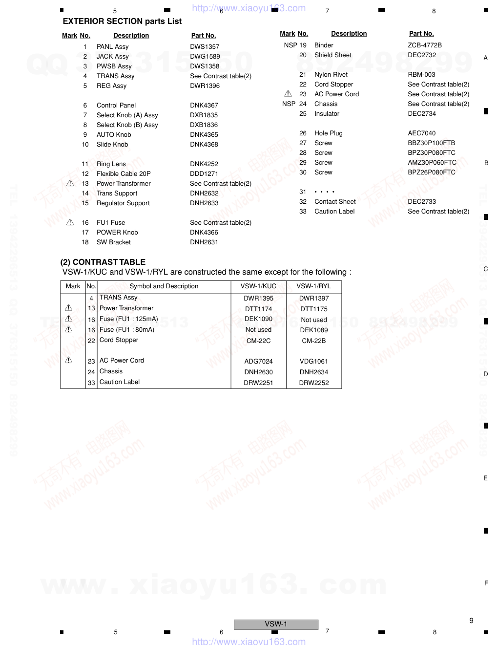
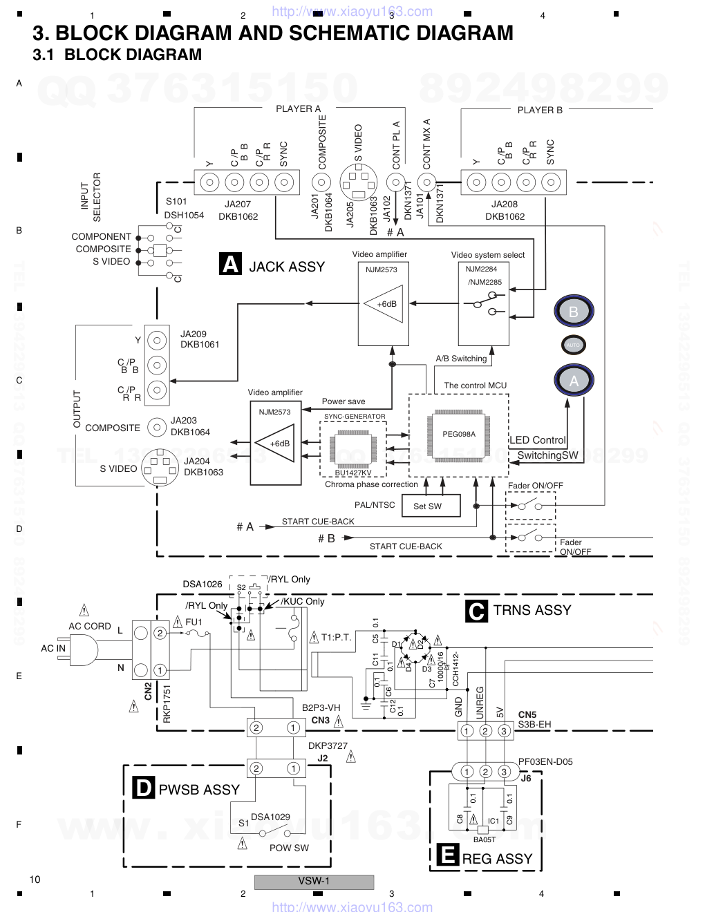
先锋PIONEER VSW-1电路图
 "先锋PIONEER VSW-1电路图-0")
 "先锋PIONEER VSW-1电路图-1")
 "先锋PIONEER VSW-1电路图-2")
 "先锋PIONEER VSW-1电路图-3")
 "先锋PIONEER VSW-1电路图-4")
 "先锋PIONEER VSW-1电路图-5")
 "先锋PIONEER VSW-1电路图-6")
 "先锋PIONEER VSW-1电路图-7")
 "先锋PIONEER VSW-1电路图-8")
 "先锋PIONEER VSW-1电路图-9")
ORDER NO. PIONEER CORPORATION 4-1, Meguro 1-chome, Meguro-ku, Tokyo 153-8654, Japan PIONEER ELECTRONICS (USA) INC. P.O. Box 1760, Long Beach, CA 90801-1760, U.S.A. PIONEER EUROPE NV Haven 1087, Keetberglaan 1, 9120 Melsele, Belgium PIONEER ELECTRONICS ASIACENTRE PTE. LTD. 253 Alexandra Road, #04-01, Singapore 159936 PIONEER CORPORATION 2004 B A VIDEO AUTO POWER OFF ON FADER START MODE SELECTOR OFF PAL NTSC ON VSW-1 RRV3045 VIDEO SWITCHER VSW-1 THIS MANUAL IS APPLICABLE TO THE FOLLOWING MODEL(S) AND TYPE(S). Model Type Power Requirement Remarks VSW-1 KUC AC120V VSW-1 RYL AC110-120V/220-240V With the voltage selector For details, refer to "Important Check Points for Good Servicing" . T-ZZR NOV. 2004 printed in Japan www. xiaoyu163. com QQ 376315150 9 9 2 8 9 4 2 9 8 TEL 13942296513 9 9 2 8 9 4 2 9 8 0 5 1 5 1 3 6 7 3 Q Q TEL 13942296513 QQ 376315150 892498299 TEL 13942296513 QQ 376315150 892498299 http://www.xiaoyu163.com VSW-1 2 1 2 3 4 1 2 3 4 C D F A B E SAFETY INFORMATION This service manual is intended for qualified service technicians; it is not meant for the casual do-it-yourselfer. Qualified technicians have the necessary test equipment and tools, and have been trained to properly and safely repair complex products such as those covered by this manual. Improperly performed repairs can adversely affect the safety and reliability of the product and may void the warranty. If you are not qualified to perform the repair of this product properly and safely, you should not risk trying to do so and refer the repair to a qualified service technician. WARNING This product contains and certain electrical parts contain chemicals which are known to the state of California to cause cancer, birth defects or other reproductive harm. Health & Safety Code Section 25249.6 – Proposition 65 NOTICE (FOR CANADIAN MODEL ONLY) Fuse symbols (fast operating fuse) and/or (slow operating fuse) on PCB indicate that replacement parts must be of identical designation. REMARQUE (POUR MODÈLE CANADIEN SEULEMENT) Les symboles de fusible (fusible de type rapide) et/ou (fusible de type lent) sur CCI indiquent que les pièces de remplacement doivent avoir la même désignation. ANY MEASUREMENTS NOT WITHIN THE LIMITS OUTLINED ABOVE ARE INDICATIVE OF A POTENTIAL SHOCK HAZARD AND MUST BE CORRECTED BEFORE RETURN- ING THE APPLIANCE TO THE CUSTOMER. 2. PRODUCT SAFETY NOTICE Many electrical and mechanical parts in the appliance have special safety related characteristics. These are often not evident from visual inspection nor the protection afforded by them necessarily can be obtained by using replacement components rated for voltage, wattage, etc. Replacement parts which have these special safety characteristics are identified in this Service Manual. Electrical components having such features are identified by marking with a on the schematics and on the parts list in this Service Manual. The use of a substitute replacement component which does not have the same safety characteristics as the PIONEER recommended replacement one, shown in the parts list in this Service Manual, may create shock, fire, or other hazards. Product Safety is continuously under review and new instructions are issued from time to time. For the latest information, always consult the current PIONEER Service Manual. A subscription to, or additional copies of, PIONEER Service Manual may be obtained at a nominal charge from PIONEER. (FOR USA MODEL ONLY) 1. SAFETY PRECAUTIONS The following check should be performed for the continued protection of the customer and service technician. LEAKAGE CURRENT CHECK Measure leakage current to a known earth ground (water pipe, conduit, etc.) by connecting a leakage current tester such as Simpson Model 229-2 or equivalent between the earth ground and all exposed metal parts of the appliance (input/output terminals, screwheads, metal overlays, control shaft, etc.). Plug the AC line cord of the appliance directly into a 120V AC 60 Hz outlet and turn the AC power switch on. Any current measured must not exceed 0.5 mA. Device under test Leakage current tester Earth ground Reading should not be above 0.5 mA Also test with plug reversed (Using AC adapter plug as required) Test all exposed metal surfaces AC Leakage Test www. xiaoyu163. com QQ 376315150 9 9 2 8 9 4 2 9 8 TEL 13942296513 9 9 2 8 9 4 2 9 8 0 5 1 5 1 3 6 7 3 Q Q TEL 13942296513 QQ 376315150 892498299 TEL 13942296513 QQ 376315150 892498299 http://www.xiaoyu163.com VSW-1 3 5 6 7 8 5 6 7 8 C D F A B E [Important Check Points for Good Servicing] In this manual, procedures that must be performed during repairs are marked with the below symbol. Please be sure to confirm and follow these procedures. 1. Product safety Please conform to product regulations (such as safety and radiation regulations), and maintain a safe servicing environment by following the safety instructions described in this manual. 1 Use specified parts for repair. Use genuine parts. Be sure to use important parts for safety. 2 Do not perform modifications without proper instructions. Please follow the specified safety methods when modification(addition/change of parts) is required due to interferences such as radio/TV interference and foreign noise. 3 Make sure the soldering of repaired locations is properly performed. When you solder while repairing, please be sure that there are no cold solder and other debris. Soldering should be finished with the proper quantity. (Refer to the example) 4 Make sure the screws are tightly fastened. Please be sure that all screws are fastened, and that there are no loose screws. 5 Make sure each connectors are correctly inserted. Please be sure that all connectors are inserted, and that there are no imperfect insertion. 6 Make sure the wiring cables are set to their original state. Please replace the wiring and cables to the original state after repairs. In addition, be sure that there are no pinched wires, etc. 7 Make sure screws and soldering scraps do not remain inside the product. Please check that neither solder debris nor screws remain inside the product. 8 There should be no semi-broken wires, scratches, melting, etc. on the coating of the power cord. Damaged power cords may lead to fire accidents, so please be sure that there are no damages. If you find a damaged power cord, please exchange it with a suitable one. 9 There should be no spark traces or similar marks on the power plug. When spark traces or similar marks are found on the power supply plug, please check the connection and advise on secure connections and suitable usage. Please exchange the power cord if necessary. 0 Safe environment should be secured during servicing. When you perform repairs, please pay attention to static electricity, furniture, household articles, etc. in order to prevent injuries. Please pay attention to your surroundings and repair safely. 2. Adjustments To keep the original performance of the products, optimum adjustments and confirmation of characteristics within specification. Adjustments should be performed in accordance with the procedures/instructions described in this manual. 4. Cleaning For parts that require cleaning, such as optical pickups, tape deck heads, lenses and mirrors used in projection monitors, proper cleaning should be performed to restore their performances. 3. Lubricants, Glues, and Replacement parts Use grease and adhesives that are equal to the specified substance. Make sure the proper amount is applied. 5. Shipping mode and Shipping screws To protect products from damages or failures during transit, the shipping mode should be set or the shipping screws should be installed before shipment. Please be sure to follow this method especially if it is specified in this manual. www. xiaoyu163. com QQ 376315150 9 9 2 8 9 4 2 9 8 TEL 13942296513 9 9 2 8 9 4 2 9 8 0 5 1 5 1 3 6 7 3 Q Q TEL 13942296513 QQ 376315150 892498299 TEL 13942296513 QQ 376315150 892498299 http://www.xiaoyu163.com VSW-1 4 1 2 3 4 1 2 3 4 C D F A B E CONTENTS SAFETY INFORMATION..................................................................................................................................... 2 1. SPECIFICATIONS ............................................................................................................................................ 5 2. EXPLODED VIEWS AND PARTS LIST ............................................................................................................ 6 2.1 PACKING SECTION .................................................................................................................................. 6 2.2 EXTERIOR SECTION............................................................................................................................... 8 3. BLOCK DIAGRAM AND SCHEMATIC DIAGRAM.......................................................................................... 10 3.1 BLOCK DIAGRAM ................................................................................................................................... 10 3.2 OVERALL WIRING DIAGRAM................................................................................................................. 12 3.3 JACK (1/3) ASSY ..................................................................................................................................... 14 3.4 JACK (2/3) ASSY ..................................................................................................................................... 16 3.5 JACK (3/3) ASSY ..................................................................................................................................... 18 3.6 PANL ASSY.............................................................................................................................................. 20 3.7 TRNS, PWSW and REG ASSYS ............................................................................................................. 22 3.8 WAVEFORMS .......................................................................................................................................... 24 4. PCB CONNECTION DIAGRAM ..................................................................................................................... 26 4.1 JACK ASSY ............................................................................................................................................. 26 4.2 PANL ASSY.............................................................................................................................................. 30 4.3 TRNS, PWSB and REG ASSYS .............................................................................................................. 32 5. PCB PARTS LIST ........................................................................................................................................... 34 6. ADJUSTMENT ............................................................................................................................................... 36 7. GENERAL INFORMATION............................................................................................................................. 37 7.1 DIAGNOSIS ............................................................................................................................................. 37 7.1.1 POWER ON SEQUENCE ................................................................................................................... 37 7.1.2 DISASSEMBLY................................................................................................................................... 38 7.2 IC ............................................................................................................................................................. 39 8. PANEL FACILITIES ........................................................................................................................................ 44 www. xiaoyu163. com QQ 376315150 9 9 2 8 9 4 2 9 8 TEL 13942296513 9 9 2 8 9 4 2 9 8 0 5 1 5 1 3 6 7 3 Q Q TEL 13942296513 QQ 376315150 892498299 TEL 13942296513 QQ 376315150 892498299 http://www.xiaoyu163.com VSW-1 5 5 6 7 8 5 6 7 8 C D F A B E 1. SPECIFICATIONS Specifications 1. General Power ..........VSW-1/RYL:AC 110-120 V/AC 220-240V, 50/60 Hz Power ............................ ............................ VSW-1/KUC : 120 V, 60 Hz Power consumption .................................. VSW-1/KUC : 8 W Power consumption ..................................... VSW-1/RYL : 9 W Operating temperature ....................................... +5°C to +35°C Storage temperature ......................................... –40°C to +60°C Operating humidity ..............5-85 % R.H. (without precipitation) Weight .............................................................................. 1.4 kg External dimensions ................. 250 (W) x 88 (D) x 87.5 (H) mm (not including connectors, buttons and other protruding parts) 2. Video input section (input level/impedance) Component video ................... BNC connectors x 3 (2 systems) Y ...................................................................... 1 Vp-p / 75 Ω CB/PB............................................................. 0.7 Vp-p / 75 Ω CR/PR............................................................. 0.7 Vp-p / 75 Ω S-Video ................................................ S connector (2 systems) Y ...................................................................... 1 Vp-p / 75 Ω C ............................................................... 0.286 Vp-p / 75 Ω Composite video ............................ RCA connector (2 systems) 1 Vp-p / 75 Ω 3. Video output section (output level/impedance) Component video ..................... BNC connectors x 3 (1 system) Y ...................................................................... 1 Vp-p / 75 Ω CB/PB............................................................. 0.7 Vp-p / 75 Ω CR/PR............................................................. 0.7 Vp-p / 75 Ω S-Video .................................................. S connector (1 system) Y ...................................................................... 1 Vp-p / 75Ω C ............................................................... 0.286 Vp-p / 75Ω Composite video .............................. RCA connector (1 system) 1 Vp-p / 75Ω 4. Sync signal output section Sync output .................................... BNC connector (2 systems) Supported video modulation systems ....................... NTSC/PAL 5. Other connectors Control input ................................... minijack (3.5 dia) 2 systems Control output ................................ minijack (3.5 dia) 2 systems 6. Accessories ¶ BNC cables.......................................................................... 2 ¶ Control cables...................................................................... 2 ¶ Operating Instructions ......................................................... 1 For improvement purposes, specifications and design may besubject to modification without notice. Note • The specifications and design of this product are subject to change without notice, due to improvement. Control Cables (ADE7108) L=1 m BNC Cable (DDE1126) L=1.5 m Accessories www. xiaoyu163. com QQ 376315150 9 9 2 8 9 4 2 9 8 TEL 13942296513 9 9 2 8 9 4 2 9 8 0 5 1 5 1 3 6 7 3 Q Q TEL 13942296513 QQ 376315150 892498299 TEL 13942296513 QQ 376315150 892498299 http://www.xiaoyu163.com VSW-1 6 1 2 3 4 1 2 3 4 C D F A B E 2. EXPLODED VIEWS AND PARTS LIST 2.1 PACKING SECTION Parts marked by "NSP" are generally unavailable because they are not in our Master Spare Parts List. The mark found on some component parts indicates the importance of the safety factor of the part. Therefore, when replacing, be sure to use parts of identical designation. Screws adjacent to mark on product are used for disassembly. For the applying amount of lubricants or glue, follow the instructions in this manual. (In the case of no amount instructions, apply as you think it appropriate.) NOTES: 3 1 8 7 2 12 10 13 14 11 9 www. xiaoyu163. com QQ 376315150 9 9 2 8 9 4 2 9 8 TEL 13942296513 9 9 2 8 9 4 2 9 8 0 5 1 5 1 3 6 7 3 Q Q TEL 13942296513 QQ 376315150 892498299 TEL 13942296513 QQ 376315150 892498299 http://www.xiaoyu163.com VSW-1 7 5 6 7 8 5 6 7 8 C D F A B E PACKING SECTION parts List (2) CONTRAST TABLE VSW-1/KUC and VSW-1/RYL are constructed the same except for the following : Mark No. Description Part No. 1 Instruction Manual See Contrast table (2) 2 BNC Cable DDE1126 3 Cord With Mini Plug ADE7108 4 • • • • 5 • • • • 6 • • • • 7 Warranty Card See Contrast table (2) NSP 8 Polyethylene Bag AHG7117 (0.06x230x340) 9 Packing Sheet DHX1008 10 Pad A DHA1629 11 Pad B DHA1630 12 Pad C DHA1631 13 Packing Case See Contrast table (2) 14 Label VRW1629 Mark No. Description Part No. Mark No. Symbol and Description VSW-1/KUC VSW-1/RYL 1 Instruction Manual (German, French, Duch, Italian, Spanish, Swedish, Chinese) Not used DRB1375 1 Instruction Manual (English) DRB1374 Not used 7 Warranty Card ARY7043 Not used 13 Packing Case DHG2486 DHG2487 www. xiaoyu163. com QQ 376315150 9 9 2 8 9 4 2 9 8 TEL 13942296513 9 9 2 8 9 4 2 9 8 0 5 1 5 1 3 6 7 3 Q Q TEL 13942296513 QQ 376315150 892498299 TEL 13942296513 QQ 376315150 892498299 http://www.xiaoyu163.com VSW-1 8 1 2 3 4 1 2 3 4 C D F A B E 2.2 EXTERIOR SECTION 27 27 27 6 28 28 28 10 10 9 1 8 7 11 11 12 2 15 29 29 14 29 16 5 13 4 30 30 30 24 25 28 25 25 28 25 26 27 22 20 21 19 27 27 17 29 18 3 B A E C D A 32 33 A 23 KUC type only RYL type only A 23 www. xiaoyu163. com QQ 376315150 9 9 2 8 9 4 2 9 8 TEL 13942296513 9 9 2 8 9 4 2 9 8 0 5 1 5 1 3 6 7 3 Q Q TEL 13942296513 QQ 376315150 892498299 TEL 13942296513 QQ 376315150 892498299 http://www.xiaoyu163.com VSW-1 9 5 6 7 8 5 6 7 8 C D F A B E EXTERIOR SECTION parts List (2) CONTRAST TABLE VSW-1/KUC and VSW-1/RYL are constructed the same except for the following : Mark No. Description Part No. 1 PANL Assy DWS1357 2 JACK Assy DWG1589 3 PWSB Assy DWS1358 4 TRANS Assy See Contrast table(2) 5 REG Assy DWR1396 6 Control Panel DNK4367 7 Select Knob (A) Assy DXB1835 8 Select Knob (B) Assy DXB1836 9 AUTO Knob DNK4365 10 Slide Knob DNK4368 11 Ring Lens DNK4252 12 Flexible Cable 20P DDD1271 > 13 Power Transformer See Contrast table(2) 14 Trans Support DNH2632 15 Regulator Support DNH2633 > 16 FU1 Fuse See Contrast table(2) 17 POWER Knob DNK4366 18 SW Bracket DNH2631 NSP 19 Binder ZCB-4772B 20 Shield Sheet DEC2732 21 Nylon Rivet RBM-003 22 Cord Stopper See Contrast table(2) > 23 AC Power Cord See Contrast table(2) NSP 24 Chassis See Contrast table(2) 25 Insulator DEC2734 26 Hole Plug AEC7040 27 Screw BBZ30P100FTB 28 Screw BPZ30P080FTC 29 Screw AMZ30P060FTC 30 Screw BPZ26P080FTC 31 • • • • 32 Contact Sheet DEC2733 33 Caution Label See Contrast table(2) Mark No. Description Part No. Mark No. Symbol and Description VSW-1/KUC VSW-1/RYL 4 TRANS Assy DWR1395 DWR1397 > 13 Power Transformer DTT1174 DTT1175 > 16 Fuse (FU1 : 125mA) DEK1090 Not used > 16 Fuse (FU1 : 80mA) Not used DEK1089 22 Cord Stopper CM-22C CM-22B > 23 AC Power Cord ADG7024 VDG1061 24 Chassis DNH2630 DNH2634 33 Caution Label DRW2251 DRW2252 www. xiaoyu163. com QQ 376315150 9 9 2 8 9 4 2 9 8 TEL 13942296513 9 9 2 8 9 4 2 9 8 0 5 1 5 1 3 6 7 3 Q Q TEL 13942296513 QQ 376315150 892498299 TEL 13942296513 QQ 376315150 892498299 http://www.xiaoyu163.com VSW-1 10 1 2 3 4 1 2 3 4 C D F A B E 3. BLOCK DIAGRAM AND SCHEMATIC DIAGRAM 3.1 BLOCK DIAGRAM AC IN S101 DSH1054 C C DKB1062 JA207 DKN1371 JA101 JA102 DKN1371 DKB1063 JA205 DKB1064 JA201 Y SYNC R R C /P C /P B B COMPOSITE S VIDEO CONT PL A CONT MX A PLAYER A SELECTOR S VIDEO INPUT COMPONENT COMPOSITE R R C /P OUTPUT S VIDEO COMPOSITE C /P B B Y JA204 JA203 DKB1064 DKB1063 DKB1061 JA209 DKB1062 JA208 C /P Y SYNC R R C /P B B PLAYER B 2 1 CN2 RKP1751 AC CORD N L T1:P.T. B2P3-VH CN3 1 2 3 CN5 S3B-EH GND FU1 5V UNREG DKP3727 J2 2 1 1 2 S1DSA1029 POW SW 1 2 3 J6 PF03EN-D05 C6 C12 D4 C11 C5 0.1 0.1 0.1 0.1 D3 C7 D1 D2 10000/16 CCH1412- IC1 BA05T C9 C8 0.1 0.1 S2 DSA1026 /RYL Only /KUC Only /RYL Only A B AUTO SwitchingSW LED Control PEG098A The control MCU A/B Switching Power save +6dB Video amplifier SYNC-GENERATOR Chroma phase correction BU1427KV NJM2573 +6dB Video amplifier Video system select NJM2573 NJM2284 /NJM2285 Fader ON/OFF Fader ON/OFF START CUE-BACK START CUE-BACK Set SW PAL/NTSC # A # A # B TRNS ASSY C REG ASSY E PWSB ASSY D JACK ASSY A www. xiaoyu163. com QQ 376315150 9 9 2 8 9 4 2 9 8 TEL 13942296513 9 9 2 8 9 4 2 9 8 0 5 1 5 1 3 6 7 3 Q Q TEL 13942296513 QQ 376315150 892498299 TEL 13942296513 QQ 376315150 892498299 http://www.xiaoyu163.com VSW-1 11 5 6 7 8 5 6 7 8 C D F A B E Ch.A Q302 Q303 Q304-Q308 Ch.B Q309-Q313 Q301 1 3 2 4 2 3 1 4 CN4 J100 S4B-EH PF04EN-D20 VLED V+5 GND GND 20 16 17 15 18 19 11 14 12 13 7 6 10 9 8 4 3 2 20 16 18 14 12 6 10 8 4 2 5 CN102 52492-2020 1 17 15 19 11 13 7 9 3 5 1 CN301 52492-2020 A-FS2OUT A-FS2IN A-FS1OUT DDD1271 A-FS1IN S305 S304 S306 S303 S302 S301 DSH1055 DSH1055 FADER START B ON/OFF FADER START A ON/OFF DSH1055 NTSC/PAL DSG1079 DSG1079 AUTO B DSG1079 A B-FS2OUT B-FS1OUT B-FS1IN B-FS2IN GNDD GNDD VLED LEDAT V+5D VLED XLEDB XLEDA XPALSW AUTOSW B-SW A-SW JA202 DKB1063 JA103 DKN1371 DKN1371 JA206 JA104 DKB1064 S VIDEO COMPOSITE CONT MX B CONT PL B AUTO Q314-Q317 # B PANL ASSY B www. xiaoyu163. com QQ 376315150 9 9 2 8 9 4 2 9 8 TEL 13942296513 9 9 2 8 9 4 2 9 8 0 5 1 5 1 3 6 7 3 Q Q TEL 13942296513 QQ 376315150 892498299 TEL 13942296513 QQ 376315150 892498299 http://www.xiaoyu163.com VSW-1 12 1 2 3 4 1 2 3 4 C D F A B E 3.2 OVERALL WIRING DIAGRAM JACK ASSY (DWG1589) S101 DSH1054 C C DKB1062 JA207 DKN1371 JA101 JA102 DKN1371 DKB1063 JA205 DKB1064 JA201 Y SYNC R R C /P C /P B B COMPOSITE S VIDEO CONT PL A CONT MX A PLAYER A SELECTOR S VIDEO INPUT COMPONENT COMPOSITE R R C /P OUTPUT S VIDEO COMPOSITE C /P B B Y JA204 JA203 DKB1064 DKB1063 DKB1061 JA209 DKB1062 JA208 C /P Y SYNC R R C /P B B PLAYER B 2 1 CN2 RKP1751 AC CORD N L T1:P.T. B2P3-VH CN3 1 2 3 CN5 S3B-EH GND FU1 5V UNREG DKP3727 J2 2 1 1 2 S1DSA1029 POW SW 1 2 3 J6 PF03EN-D05 TRNS ASSY (/KUC : DWR1395) (/RYL : DWR1397) PWSB ASSY (DWS1358) REG ASSY (DWR1396) /KUC : DDT1174 /RYL : DTT1175 /KUC : DEK1090 T125mAL250V /RYL : DEK1089 T80mAL250V /KUC:ADG7024 /RYL:VDG1061 A 1/3 - A 3/3 A D C E www. xiaoyu163. com QQ 376315150 9 9 2 8 9 4 2 9 8 TEL 13942296513 9 9 2 8 9 4 2 9 8 0 5 1 5 1 3 6 7 3 Q Q TEL 13942296513 QQ 376315150 892498299 TEL 13942296513 QQ 376315150 892498299 http://www.xiaoyu163.com VSW-1 13 5 6 7 8 5 6 7 8 C D F A B E /RYL Only 1 3 2 4 2 3 1 4 CN4 J100 S4B-EH PF04EN-D20 VLED V+5 GND GND 20 16 17 15 18 19 11 14 12 13 7 6 10 9 8 4 3 2 20 16 18 14 12 6 10 8 4 2 5 CN102 52492-2020 1 17 15 19 11 13 7 9 3 5 1 CN301 52492-2020 A-FS2OUT A-FS2IN A-FS1OUT DDD1271 A-FS1IN S305 S304 S306 S303 S302 S301 DSH1055 DSH1055 FADER START B FADER START A DSH1055 NTSC/PAL DSG1079 DSG1079 AUTO B DSG1079 A B-FS2OUT B-FS1OUT B-FS1IN B-FS2IN GNDD GNDD VLED LEDAT V+5D VLED XLEDB XLEDA XPALSW AUTOSW B-SW A-SW ON/OFF ON/OFF JA202 DKB1063 JA103 DKN1371 DKN1371 JA206 JA104 DKB1064 S VIDEO COMPOSITE CONT MX B CONT PL B PANL ASSY (DWS1357) B S2 DSA1026 SELECTOR VOLTAGE 110-120V / 220-240V NOTES: • When ordering service parts, be sure to refer to “EXPLODED VIEWS and PARTS LIST” or “PCB PARTS LIST”. • The > mark found on some component parts indicates the importance of the safety factor of the part. Therefore, when replacing, be sure to use parts of identical designation. • : The power supply is shown with the marked box. www. xiaoyu163. com QQ 376315150 9 9 2 8 9 4 2 9 8 TEL 13942296513 9 9 2 8 9 4 2 9 8 0 5 1 5 1 3 6 7 3 Q Q TEL 13942296513 QQ 376315150 892498299 TEL 13942296513 QQ 376315150 892498299 http://www.xiaoyu163.com VSW-1 14 1 2 3 4 1 2 3 4 C D F A B E 3.3 JACK (1/3) ASSY IN A COMPONENT C /P R R C /P B B SYNC A Y JA207 DKB1062 SYNCA COMPONENT IN B C119 C120 R201 C121 R202 R203 75F 75F 75F C201 C256 (A-YIN) 0.01 C257 C202 0.01 10/16 2.2/50 B-CB B-CB B-CR B-Y A-CB B-CR A-CR INYUV A-CB B-Y A-CR A-Y A-Y C258 C203 (A-CbIN) (A-CrIN) 10/16 0.01 C269 C216 C205 C260 C259 C204 (B-CbIN) (B-CrIN) STBY (B-YIN) 10/16 10/16 0.01 GNDV 2.2/50 0.01 SYNCB JA208 SYNC B C /P B B C /P R R Y GNDV DKB1062 C122 C123 R210 C124 R211 R212 75F 75F 75F 0.01 STBY A-SC INSCMP B-SY B-CMP A-SY A-CMP A-CMP B C R213 R218 JA201 C130 C270 C140 R214 Q201 R217 R557 COMPOSITE IN A (A-CMPIN) DKB1064 75F 0.01 100/10 33k 20k 2SC4081(QRS) V5VA V+5V V+5V A-SY B-CMP E B C E B C E C282 R232 Q203 L59 C142 C131 R215 R231 R216 R220 Q202 JA202 C271 C141 R219 R558 IN B COMPOSITE (B-CMPIN) 100/10 0.01 33k 1k 2SC4081(QRS) 20k VTL1077 100/10 75F 33k 1k GNDV DKB1064 0.01 2SC4081(QRS) V5VB 1k D111 R227 D110 R228 JA205 (A-SYIN) DKB1063 75F GNDV V5VA A-SC B C C208 C283 L60 C143 R233 IN A S VIDEO 0.01 GNDV UDZS6R2(B) 0.01 VTL1077 UDZS6R2(B) 2SC4081(QRS) 20k 20k B-SY B E C E R246 R249 Q205 D113 R229 D112 R230 R234 Q204 (A-SCIN) 1k UDZS6R2(B) UDZS6R2(B) 33k 2SC4081(QRS)-TLB V5VB 75F 10/16 33k 1k C254 C145 L62 D117 R245 D116 C253 L61 C144 R235 JA206 (B-SCIN) IN B S VIDEO (B-SYIN) 0.01 GNDV VTL1077 UDZS6R2(B) UDZS6R2(B) DKB1063 75F 0.01 VTL1077 20k GNDV 100/10 E B C D127 R247 D126 R251 R248 Q206 R250 UDZS6R2(B) GNDV UDZS6R2(B) 75F 10/16 33k 1k 2SC4081(QRS)-TLB 20k B-SC C209 0.01 CP/XYC R137 C180 C181 R138 0.1 1M 0.1 1M GNDV NJM2285V IC203 IN1A IN1B V+ GND1 IN2B CNT1 OUT1 GND2 IN2A CTL2 OUT2 OUT3 IN3B GND3 CNT3 IN3A 16 15 14 13 12 11 10 9 2 1 4 3 6 5 8 7 A-SC A-SY A-CMP 1 2 C237 R530 C231 C230 C227 R529 R528 R527 R136 R135 NP 10/16 10/16 10/16 10/16 100k 100k GNDV V+5V GNDV C225 0.1 XA/B B-SC C297 C268 C272 R525 C218 C296 C295 C264 10/16 0.01 10/16 0.1 GNDV 10/16 10/16 0.01 0.01 R524 R133 C294 C263 R523 R522 C262 R521 R132 R131 IC202 C293 C292 C261 R526 L14 R134 C45 100k 10/16 0.01 0.01 100k 100k 10/16 0.01 100k V+5V 0.1 16 14 15 13 12 11 9 10 1 2 3 4 5 8 6 7 IN1A GND1 IN2B V+ CTL2 IN2A IN3B GND3 IN1B CTL1 OUT1 OUT2 OUT3 CTL3 GND2 IN3A NJM2285V 16 1 15 14 13 12 11 10 6 7 2 3 4 5 9 8 R551 R550 R549 R548 R552 R553 R143 IC211 0 0 0 0 0 0 0 IN1A IN1B R504 IN2B GND1 V+ CTL2 GND3 IN2A OUT3 CTL3 GND2 CTL1 OUT1 OUT2 IN3B IN3A NJM2284V V+5V 100k XA/B C195 R144 GNDV 0.1 100k 0 0 0 0 0 0 0 0 0 0 0 0 A 1/3 A 3/3 A 3/3 A 3/3 A 2/3 A 2/3 (Y) (Cb) (Cr) VIDEO SWICH VIDEO SWICH VIDEO SWICH IC211 PIN No Voltage Condition 2, 7, 12 0V Ach SELECT 4, 10, 15 0V 13 4.74V IC202 PIN No Voltage Condition 2, 7, 12 0V Ach SELECT 4, 10, 15 0V 13 4.74V IC203 PIN No Voltage Condition 2 , 7, 12 0V 4.67V S101 : S VIDEO : Other 4, 10, 15 0V 13 4.75V 14 13 www. xiaoyu163. com QQ 376315150 9 9 2 8 9 4 2 9 8 TEL 13942296513 9 9 2 8 9 4 2 9 8 0 5 1 5 1 3 6 7 3 Q Q TEL 13942296513 QQ 376315150 892498299 TEL 13942296513 QQ 376315150 892498299 http://www.xiaoyu163.com VSW-1 15 5 6 7 8 5 6 7 8 C D F A B E Notes is STBY RESISTOR CAPACITOR NO MARK F NO MARK CERAMIC CH NO MARK ELCTROLYTIC NP AL RS1/16S***J RS1/16S****F Ω CKSRYB µ F CCSRCH µ F CEJQ µ F/V CEJQNP µ F/V CEAL F/V 7 6 5 8 10 9 4 3 2 1 12 13 11 14 C28 C25 C27 C23 C24 C26 R556 R555 R554 IC214 0 0 0 VIN2 VIN3 GND1 VOUT3 GND2 BI/XCL PSAVE VIN1 VSAG1 V1 VOUT1 VSAG2 VOUT2 V2 NP 10/16 0.01 10/16 NP 0.01 0.01 10/16 NP NJM2573V V+5H R145 C206 C207 C125 GNDV 100k 0.1 0.1 22/16 C22 C267 R206 C215 C266 C214 C265 C213 R205 R204 22/16 330/6.3 0.01 AL 75F 330/6.3 0.01 330/6.3 0.01 75F AL 75F AL C286 C288 C287 JA209 B B C /P Y R R COMPONENT OUT C /P GNDV DKB1061 R226 C279 C228 R224 C280 C229 C277 C226 R222 C278 C224 L64 L63 0.01 75F 10/16 AL 330/6.3 75F 0.01 22/16 0.01 75F AL 330/6.3 22/16 VTL1077 VTL1077 C276 R146 R147 C219 C222 C275 C221 R536 C274 R537 R535 C220 IC210 R505 VIN3 GND1 VIN2 VIN1 PSAVE VSAG1 0.01 NP 10/16 GNDV 100k 0.1 NJM2573V 10/16 NP 0.01 NP 10/16 V+5V 0.01 7 6 5 4 3 12 11 9 10 8 2 1 13 14 VOUT3 VOUT2 GND2 VSAG2 BI/XCL V1 VOUT1 V2 C223 C129 22/16 0.1 100k JA204 C289 JA203 YG COMPOSITE OUT GNDV DKB1063 GNDV DKB1064 D129 D131 D130 D128 CG C Y S VIDEO OUT UDZS6R2(B) UDZS6R2(B) GNDV UDZS6R2(B) UDZS6R2(B) B-CHROMA B-CSYNC A-CHROMA A-CSYNC B-SC B-CMP B-SY 15 16 14 13 1 3 2 4 11 10 12 9 5 6 8 7 C273 R534 C246 C242 R533 R532 IC206 C241 R531 R139 R140 C281 C21 GND1 IN1A CNT1 IN1B V+ IN2B GND2 OUT1 CNT3 CTL2 GND3 IN2A OUT3 IN3B IN3A OUT2 10/16 NP 10/16 10/16 10/16 100k 100k GNDV GNDV 0.1 V+5V 47/16 C182 R141 C183 R142 0.1 1M 1M 0.1 NJM2285V GNDV 0 0 0 0 0 0 0 0 A 1/3 A 1/3 JACK ASSY (DWG1589) A 2/3 : S-VIDEO OUT C SIGNAL (A-SC) (A-SY) (O-SY) : COMPOSITE-A (A-CMP) (O-CMP) (O-SY) : S-VIDEO OUT Y : S-VIDEO OUT C (O-SC) (O-SC) (O-CMP) (O-CMP) : S-VIDEO OUT Y SIGNAL : COMPOSITE-OUT : Y COMPONENT OUT (O-Y) (O-Cb) (O-Cr) : Cr SIGNAL ROUTE (A ch) : VIDEO SIGNAL ROUTE (Cr) (Y) (Cb) (O-Cr) : Cr COMPONENT OUT (O-Cb) (O-Y) : Cb COMPONENT OUT : Y SIGNAL ROUTE (A ch) : Cb SIGNAL ROUTE (A ch) VIDEO AMP VIDEO AMP VIDEO SWICH IC206 PIN No Voltage Condition 2, 7, 12 0V 4.67V S101 : S VIDEO : Other 4, 10, 15 0V 13 4.74V 10 11 12 7 8 9 4 5 6 3 2 1 www. xiaoyu163. com QQ 376315150 9 9 2 8 9 4 2 9 8 TEL 13942296513 9 9 2 8 9 4 2 9 8 0 5 1 5 1 3 6 7 3 Q Q TEL 13942296513 QQ 376315150 892498299 TEL 13942296513 QQ 376315150 892498299 http://www.xiaoyu163.com VSW-1 16 1 2 3 4 1 2 3 4 C D F A B E 3.4 JACK (2/3) ASSY G-OSD:64 R-D7:63 R-D6 R-D5 I/O-VDD R-D4 R-D3 R-OSD R-D2 VCLK:51 PAL60B:50 YFIL:49 Y-OUT A-VDD Y-GND R-D1 R-D0 CLK-SW RST YFIL VDD Y/C-OFF OSD-SW CDGSWB B-D3 B-D2 B-D1 B-D0 18:B-D5 17:B-D4 B-D7 B-D6 GND G-D7 G-D5 G-D6 G-D4 G-D3 G-D2 G-D0 G-D1 B-OSD VSYNC PAL/NTSC TEST-0 IM-1 IM-0 GND ADDH 32:INTERACE 31:I/O-VDD PIX-CLK VDD TEST-1 V-SYNC C-GND SLAB V-GND VREF C-OUT V-OUT A-VSS P-VDD IR IC151 19 18 21 17 22 23 25 24 20 27 28 26 31 29 30 32 34 36 37 38 35 33 62 63 64 60 59 61 58 57 56 39 40 43 42 41 44 45 46 47 55 53 54 52 51 50 49 48 BU1427KV C146 C149 1 47/16 1.0 15 16 14 13 12 11 9 10 8 7 6 4 5 3 2 R159 AKF7001- 27M R278 R123 C148 TP1 V+5D 220 0.01 0 /RESET 27M adjust C169 C170 X151 GNDD 0 VCM1012-VC1 27MHz CJ 1p DSS1155 7WU04FU CH 8p IC152 R164 1M IC152 R148 R166 IC152 7WU04FU V+5D 820 7WU04FU 3 8 4 5 2 6 8 4 4 1 7 8 C44 C168 GNDD 1.0 1.0 PAL/XNT GNDD C234 R238 C250 R236 CH 56p GNDV 1K 1/50 390 A-CHROMA A-CSYNC C284 C251 IC212 0.1 GNDV V+5V 1/50 TC74HC4066AFT GNDV YA YA C244 R253 C235 R239 L203 IC212 L201 4 7 3 14 5 7 2 1 13 14 56p CH 1K 390 22u GNDV GNDV TC74HC4066AFT 33u C210 X201 IC212 C232 R237 C233 14 8 9 7 6 VSS1075 3.579545MHz CH 12p GNDV GNDV TC74HC4066AFT 0.01 220k CH 560p IC212 C211 X202 11 7 10 12 14 4.433618MHz CH 8p VSS1094 TC74HC4066AFT R252 C243 GNDV GNDV 560p 220k CH 0.01 GNDV R240 R207 C236 C252 C127 GNDV GNDV 0.47 GNDV 1k 4.7/25 R279 5.1k 0 2.2/50 R208 C255 R241 R115 R116 C245 C128 GNDV GNDV GNDV 4.7/25 1k 0.47 R282 0 0 0 5.1k 2.2/50 CH C212 X203 IC213 7 9 8 6 14 CH 12p TC74HC4066AFT CH C217 X204 11 10 12 14 CH 8p 3.579545MHz VSS1075 IC213 7 VSS1094 4.433618MHz TC74HC4066AFT Q207 E C B GNDV GNDV DTC124EUA Q210 E C B DTC124EUA Q208 E C B DTC124EUA YA IC213 L204 7 1 14 2 13 TC74HC4066AFT 33u YA C285 IC213 L205 7 3 14 4 5 0.1 GNDV V+5V GNDV 22u TC74HC4066AFT C166 IC209 IC209 4 4 7 1 8 6 2 8 7WU04F 7WU04F GNDV 0.1 IC209 4 3 8 5 7WU04F V+5V PLL_RESET_B PLL_RESET_A PAL/XNT B-CHROMA B-CSYNC Q209 E B C GNDV GNDV GNDV GNDV DTC124EUA (VSYNC) C39 C42 C40 C43 R168 C171 R167 R165 C172 R162 C41 1.0 1.0 1.0 1.0 0.1 75F 75F 1.2kF 1.0 1.0 75F GNDD GNDD VSYNC AKF7001- adjust pin TP2 (for FC) C159 R169 L150 L152 L151 C160 L153 330p 0 CH 1u 1u 1u 330p 1u CH C161 C162 L154 L155 L157 L156 330p 330p 1u CH 1u 1u CH 1u C B NC GND INH IO5 A IO3 IO7 IOCOM IO6 IO0 IO1 IO2 IO4 VCC C158 IC153 8 7 1 4 2 5 6 3 9 10 11 12 14 13 15 16 GNDD 0.1 TC74HC4051AFT V+5D SDLYA1 SDLYA2 SDLYA0 R124 R121 A 2/3 A 1/3 A 3/3 A 3/3 A 3/3 A 1/3 A 3/3 A 3/3 SYNC-GENERATOR APC FILTER APC FILTER IC209 PIN No Voltage Condition 1 4.74V 0V PAL SELECT NTSC SELECT 2 4.74V 0V PAL SELECT NTSC SELECT 4 0V 7 0V 4.74V PAL SELECT NTSC SELECT 8 4.74V P22 4.74V 0V PAL SELECT NTSC SELECT 0V 0V 4.74V 4.74V 2.47V 0V 0V 0V 4.74V 4.74V 0V 4.74V 4.74V 4.74V 15 16 17 www. xiaoyu163. com QQ 376315150 9 9 2 8 9 4 2 9 8 TEL 13942296513 9 9 2 8 9 4 2 9 8 0 5 1 5 1 3 6 7 3 Q Q TEL 13942296513 QQ 376315150 892498299 TEL 13942296513 QQ 376315150 892498299 http://www.xiaoyu163.com VSW-1 17 5 6 7 8 5 6 7 8 C D F A B E RESISTOR CAPACITOR INDUCTOR NO MARK F NO MARK CERAMIC CH CK NO MARK ELCTROLYTIC AL NO MARK YA Notes RS1/16S***J Ω RS1/16S****F CKSRYB µ F CCSRCH µ F CCSRCK µ F CEJQ µ F/V CEAL µ F/V LCTC H LCYA H is STBY IC208 C248 0.01 7WHU04FU GNDV MM1093NF GNDV 4 2 6 8 R281 R502 IC208 R257 R256 C247 C138 C139 V+5V 0.01 7WHU04FU GNDV GNDV 4.3k 390p 12k CH 0.1 GNDV 22/16 NC fscout GND1 GND2 APCfil1 X'tal VCC1 OSCR OSCC VCC2 4fscout APCfil2 CHROMAin ACCfil BURSTGATE CMPSin IC207 8 7 5 6 4 3 9 10 12 11 14 13 2 1 15 16 C239 R274 R244 33 GNDV MM1093NF GNDV 1M NC OSCR fscout GND2 X'tal GND1 APCfil1 ACCfil VCC1 VCC2 APCfil2 OSCC 4fscout BURSTGATE CHROMAin CMPSin IC204 7 8 6 4 5 3 2 9 10 13 11 12 15 14 1 16 MA R280 R501 R243 R242 C238 C136 C137 V+5V GNDV GNDV 4.3k 12k 390p C132 0.01 C133 0.01 CH GNDV 0.1 22/16 XOE 7 1 4 8 R546 R547 C155 C153 0.1 0.1 VIN3 VIN2 GND1 GND2 BI/XCL VOUT3 PSAVE V1 VIN1 VSAG1 VOUT1 VOUT2 V2 VSAG2 IC155 6 7 8 9 5 3 1 4 2 12 10 13 11 14 GNDV NJM2573V 0.1 C154 V+5C C152 C190 C177 R154 C175 C176 R506 C178 R153 V+5V 47/6.3 0.1 22/16 75F 10/16 47/6.3 75F 10/16 C240 C191 C249 R503 C192 R273 C193 C194 R271 R272 GNDV SN0406014PW 0.1 0.1 V+5V GNDV 22/16 10k 10k 0.01 0.01 0.01 10k IC208 3 8 4 5 GNDV 7WHU04FU B C157 GNDV PLL2 PLL3 PLL1 SYNCB (B-SYNC) SYNC out (A-SYNC) C156 GNDV SYNCA INH VCOout GND C1b C1a COMPin DEMout VCOin R1 R2 SIGin PC2out PC1out PCPout VCC PC3out IC205 8 6 7 3 4 5 9 10 11 12 14 13 2 1 16 15 R157 R158 C174 R152 Q109 C104 B E C GNDV 33k 1k GNDV V+5C 10/16 22k 2SC4081(QRS) GNDD 10/16 SDLYB2 SDLYB1 SDLYB0 INH NC GND A B C IO7 VCC IO6 IO4 IOCOM IO5 IO0 IO1 IO2 IO3 C167 C150 C151 IC154 8 7 9 10 1 6 3 2 4 5 12 15 13 11 14 16 GNDD 0.1 TC74HC4051AFT 47/16 0.1 V+5D C163 C165 C164 L158 L159 L160 L161 L162 L163 R160 330p 330p 330p 1u 1u CH CH 1u 1u 1u 1u CH 75F R155 C298 R156 C173 R151 Q108 B C E GNDV 33k 10/16 GNDV 1k 10/16 22k V+5C 2SC4081(QRS) A R275 R258 33 1M 0 0 0 0 0 0 A 2/3 A 2/3 JACK ASSY (DWG1589) A 3/3 A 1/3 A 3/3 A 1/3 VIDEO AMP DELAY CIRCUIT CLOCK GENERATOR CLOCK GENERATOR CHROMA PHASE COMPARATOR 18 19 20 21 22 www. xiaoyu163. com QQ 376315150 9 9 2 8 9 4 2 9 8 TEL 13942296513 9 9 2 8 9 4 2 9 8 0 5 1 5 1 3 6 7 3 Q Q TEL 13942296513 QQ 376315150 892498299 TEL 13942296513 QQ 376315150 892498299 http://www.xiaoyu163.com VSW-1 18 1 2 3 4 1 2 3 4 C D F A B E 3.5 JACK (3/3) ASSY C C R600 VLED C100 22/16 R270 V+5D V+5V GNDD GNDV 0 R601 GNDD C101 47/16 R602 GNDV C102 C103 GNDD 47/16 0.1 GND GND V+5 VLED J100 PF04EN-D20 1 2 3 4 /RESET (RESET) R103 V+5D 4.7k R104 C126 R102 CH 330p 8.2k(F) 3.3k(F) M51957BFP GNDD 4 3 2 1 5 8 6 7 IC100 C107 C105 C108 0.1 33p 0.1 CH CONPONENT COMPOSITE S VIDEO S101 C116 R119 R117 DSH1054 GNDD 100p 100 100 CMP-SW NC-SW C117 D114 D115 R120 R118 100p CH CH DA221 GNDD DA221 22k V+5D 22k V+5D GNDD GNDD CONT PL B CONT MX B FADER START CONT PL A CONT MX A JA101 DKN1371 JA102 DKN1371 JA103 DKN1371 JA104 DKN1371 C51 C52 L39 L38 GNDV VTL1076 VTL1076 A-FS2IN A-FS1IN R109 R107 100 100 A-FS2OUT A-FS1OUT L41 L40 VTL1076 VTL1076 B-FS2IN B-FS1IN C55 C56 L43 L42 C53 C54 GNDV VTL1076 VTL1076 GNDV B-FS1OUT B-FS2OUT C57 C58 L45 L44 GNDV VTL1076 VTL1076 D102 C114 C113 100p 100p CH UDZS6R2(B) CH B B E C C E D101 R108 D105 Q105 D107 Q104 R110 GNDV GNDD UDZS6R2(B) 10k 1SS355 DTA144EUA 1SS355 DTA144EUA 10k V+5D B C111 D104 C112 D103 R113 R111 D106 D108 Q102 100p 100p GNDV UDZS6R2(B) UDZS6R2(B) CH CH 100 100 1SS355 D118 D119 RB751V-40 RB751V-40 1SS355 V+5D DTA144EUA B C C E E R112 R114 Q103 GNDD 10k 10k DTA144EUA TRANS SSY (CN4) C Switches JACK Assy S101 : INPUT SELECTOR 0 0 0 JACK ASSY (DWG1589) A 3/3 A 3/3 A 2/3 RESET IC IC100 PIN No Voltage Condition 2 1.35V 4 0V 5 1.24V 6 4.74V 7 4.74V www. xiaoyu163. com QQ 376315150 9 9 2 8 9 4 2 9 8 TEL 13942296513 9 9 2 8 9 4 2 9 8 0 5 1 5 1 3 6 7 3 Q Q TEL 13942296513 QQ 376315150 892498299 TEL 13942296513 QQ 376315150 892498299 http://www.xiaoyu163.com VSW-1 19 5 6 7 8 5 6 7 8 C D F A B E 18 20 19 15 16 17 14 12 13 11 10 9 7 8 6 5 4 3 1 2 B-FS2IN B-FS1OUT B-FS2OUT B-FS1IN LEDAT XLEDB XPALSW XLEDA AUTOSW A-SW B-SW A-FS2IN A-FS2OUT A-FS1OUT A-FS1IN GNDD GNDD VLED VLED V+5D CN102 52492-2020 V+5D VLED GNDD PAL/XNT VSYNC PLL_RESET_A PLL_RESET_B XA/B CP/XYC FW R101 C115 GNDD 330 for FLASH Rx Tx GND FW R106 C110 10k V+5D 0.1 25 24 21 22 23 20 19 18 17 16 15 14 13 12 11 5 8 10 3 9 4 7 6 2 1 100 SDLYB1 SDLYB2 52: 51: 54:N 53:N 77:Vref 76:AVCC AIN3 AIN4 DA0 AIN2 AIN1 AIN5 PAL/XNT AVSS PEG098A8 VSYNC VSS VSS SCK1 SRX1 SRX0 SCK0 STX0 STX1 VSS FWE TEST1 IC101 HD64F3062BFBL25 SDLYB0 SDLYA2 SDLYA0 SDLYA1 A-SW B-SW AUTOSW XPALSW XLEDA LEDAT XLEDB N N N N VSS N STBY φ VSS NMI XRST VCC XTAL EXTAL CMP-SW MD1 MD0 NC-SW VSS N XOE A-FS2IN A-FS1IN AIN0 B-FS2IN B-FS1IN VCC MD2 N 75 76 78 77 84 83 80 79 81 82 86 85 87 88 89 91 90 94 92 95 93 97 96 99 98 PLL1 PLL3 PLL2 C E B (MD2) Q101 R105 C109 DTC124EUA GNDD 1k V+5D 0.1 51 52 55 54 53 58 56 57 59 61 62 60 63 64 65 66 67 68 69 71 70 73 72 74 50 49 48 47 46 44 45 42 43 40 39 41 37 38 35 36 30 29 34 33 31 32 27 28 26 /RESET MA 24.576Hz R277 X101 R122 C106 V+5D DSS1139 0 GNDD GNDD 10k V+5D 0.1 C118 C147 0.1 0.01 XOE PANL ASSY (CN301) B is STBY Notes RESISTOR CAPACITOR F NO MARK NO MARK CERAMIC CH NO MARK ELCTROLYTIC RS1/16S****F Ω RS1/16S***J Ω CKSRYB µ F CCSRCH µ F CEJQ µ F/V A 3/3 A 1/3 A 2/3 A 2/3 A 2/3 CPU IC IC101 PIN No Voltage Condition 2 0 3 0 11 0 18 4.67V 4.67V 0V S101: COMPONENT : COMPOSITE : S VIDEO 19 0V 4.67V Ach SELECT Bch SELECT 22 0V 32 0V 4.76V AUTO ON AUTO OFF 33 4.74V 0V Ach SELECT Bch SELECT 34 0V 4.74V Ach SELECT Bch SELECT 35 4.75V 36 0V 4.74V PAL SELECT NTSC SELECT 37 4.74V 38 4.74V 39 4.74V PIN No Voltage Condition 40 0V 41 0V 42 0V 43 0V 44 0V 57 0V 63 4.74V 65 0V 68 4.75V 71 0V 4.74V S101: COMPOSITE : Other 72 0V 4.74V S101: COMPONENT : Other 75 4.74V 86 0V 89 4.74V 0V PAL SELECT NTSC SELECT 92 0V www. xiaoyu163. com QQ 376315150 9 9 2 8 9 4 2 9 8 TEL 13942296513 9 9 2 8 9 4 2 9 8 0 5 1 5 1 3 6 7 3 Q Q TEL 13942296513 QQ 376315150 892498299 TEL 13942296513 QQ 376315150 892498299 http://www.xiaoyu163.com VSW-1 20 1 2 3 4 1 2 3 4 C D F A B E 3.6 PANL ASSY AUTOSW B-SW A-SW V+5D GNDD GNDD DSG1079 100 DA221 GNDD GNDD GNDD 100p 100p 100p DA221 DSG1079 100 DSG1079 100 V+5D 10k DA221 10k 10k C301 S303 R306 C302 C303 D313 S302 R305 S301 R304 R301 D312 R303 R302 D311 NTSC/PAL CH AUTO CH CH B Video SW A A-FS2OUT A-FS2IN A-FS1IN A-FS1OUT XPALSW DSH1055 GNDD DSH1055 100 100p GNDD DA221 GNDD CH 10k S304 R309 S306 R308 D314 C308 ON OFF FADER_START_A ON OFF B-FS2OUT B-FS2IN B-FS1IN B-FS1OUT DSH1055 S305 FADER_START_B 20 18 19 17 16 14 15 12 13 11 10 B-FS2OUT B-FS1OUT B-FS2IN B-FS1IN LEDAT XLEDB V+5D GNDD GNDD 0.01 100/10 GNDD 100/16 0.01 C321 C322 C317 C337 C336 C334 C335 C318 C333 C332 STBY GNDD GNDD V+5D VLED VLED 8 6 4 2 XLEDA XPALSW TOP B-SW AUTOSW A-SW A-FS2OUT A-FS1OUT A-FS2IN A-FS1IN 52492-2020 V+LED C331 C330 C328 C329 C327 C325 C326 C324 C323 CN301 STBY 9 7 5 3 1 JACK ASSY(CN102) A B PANL ASSY (DWS1357) B Switches PANL Assy S301 : Video A S302 : Video B S303 : Video Auto S304 : Fader Start A S305 : Fader Start B S306 : NTSC / PAL www. xiaoyu163. com QQ 376315150 9 9 2 8 9 4 2 9 8 TEL 13942296513 9 9 2 8 9 4 2 9 8 0 5 1 5 1 3 6 7 3 Q Q TEL 13942296513 QQ 376315150 892498299 TEL 13942296513 QQ 376315150 892498299 http://www.xiaoyu163.com VSW-1 21 5 6 7 8 5 6 7 8 C D F A B E Notes RESISTOR CAPACITOR is STBY NO MARK NO MARK CERAMIC CH NO MARK ELCTROLYTIC RS1/16S***J Ω CKSRYB µ F CCSRCH µ F CEJQ µ F C B E E E E E C B B B C C B C E C B XLEDB XLEDA 270 SLR-343BBT(FGHJ) SLR-343BBT(FGHJ) SLR-343BBT(FGHJ) DTA124EUA 0.01 0.01 V+5D GNDD 2SC4081(QRS) 2SC4081(QRS) 2SC4081(QRS) 18 18 2SC4081(QRS) 18 18 2SC4081(QRS) 270 SLR-343BBT(FGHJ) SLR-343BBT(FGHJ) SLR-343BBT(FGHJ) SLR-343BBT(FGHJ) 0.01 DTA124EUA 0.01 V+5D R315 D305 C311 D306 D307 C312 C313 Q303 R314 Q304 R316 Q305 Q306 R317 R318 Q307 Q308 R307 D301 D302 D303 D308 Q302 C304 C306 0.01 C305 C B E E C E B B C B LEDAT DTA124EUA SLI-343YCW(RST) SLI-343YCW(RST) V+5D 0.01 2SC4081(QRS) 0.01 GNDD 18 2SC4081(QRS) 18 2SC4081(QRS) 2SC4081(QRS) 2SC4081(QRS) D309 C320 C319 Q301 R324 R326 Q309 Q310 Q311 E E C B C E B C 18 18 18 0.01 R327 R328 Q312 Q313 R329 C314 LED-B E C E B B B C E C GNDD 2SC4081(QRS) 2SC4081(QRS) 2SC4081(QRS) 18 18 18 270 R331 R333 R332 Q317 Q315 Q314 R334 D310 LED-AUTO E B C 18 SLR-343BBT(FGHJ) 0.01 0.01 V+LED R319 D304 C307 LED-A B www. xiaoyu163. com QQ 376315150 9 9 2 8 9 4 2 9 8 TEL 13942296513 9 9 2 8 9 4 2 9 8 0 5 1 5 1 3 6 7 3 Q Q TEL 13942296513 QQ 376315150 892498299 TEL 13942296513 QQ 376315150 892498299 http://www.xiaoyu163.com VSW-1 22 1 2 3 4 1 2 3 4 C D F A B E 3.7 TRNS, PWSW and REG ASSYS CN3 B2P3-VH 2 1 1 2 H2 H1 CN2 AKR7001 AC CORD N L FU1 DEK1089 T80mAL250V FU1 DEK1090 T125mAL250V RKP1751-A AKR7001 AC Input C2 L20 C3 ACE7027 VTL-004- ACE7027 DKP3732 8 7 6 10 9 11 12 13 T1 S2 DSA1026 110-120V / 220-240V SELECTOR VOLTAGE P.T. 5 4 3 1 2 J4 CAUTION REPLACE WITH SAME TYPE AGAINST RISK OF FIRE, AND RATINGS OF FUSE FOR CONTINUED PROTECTION B2P3-VH 1 2 CN3 CAUTION FOR CONTINUED PROTECTION AGAINST RISK OF FIRE, REPLACE ONLY WITH SAME TYPE NO.218.125 MFD. BY LITTEL FUSE INC. FOR FU1. AC CORD 1 N L 2 CN2 RKP1751 AKR7001 AKR7001 AC Input H2 H1 ACE7027 ACE7027 VTL-004- L20 C2 C3 DKP3733 J3 P.T. T1 VDG1061 ADG7024 TRNS ASSY (/RYL : DWR1397) C D C TRNS ASSY (/KUC : DWR1395) C D DTT1175 DTT1174 J2 www. xiaoyu163. com QQ 376315150 9 9 2 8 9 4 2 9 8 TEL 13942296513 9 9 2 8 9 4 2 9 8 0 5 1 5 1 3 6 7 3 Q Q TEL 13942296513 QQ 376315150 892498299 TEL 13942296513 QQ 376315150 892498299 http://www.xiaoyu163.com VSW-1 23 5 6 7 8 5 6 7 8 C D F A B E The mark found on some component parts should be replaced with same parts (safety regulation authorized) of identical designation. Notes CAPACITOR NO MARK CERAMIC NO MARK ELECTROLYTIC STBY is STANBY : CKSRYB µ F : CEJQ µ F C6 C12 J1 D4 C11 C5 0.1 DE012WF0 0.1 0.1 0.1 RB060L-40 RB060L-40 RB060L-40 RB060L-40 D4 D3 D2 D1 3 1 2 D3 C7 D1 D2 C10 IC4 IC3 CN5 10000/16 100/10 AEK7005 ICP-N15 S3B-EH CCH1412- C1 S1 0.01 ACG7039-A DSA1029-A Board in Connector ASSY J2 DKP3727- AC-ON/OFF 2 1 POW SW 1 2 3 4 CN4 S4B-EH GND GND VLED V+5 IC1 BA05T C9 C8 0.1 0.1 1 2 3 J6 PF03EN-D05 JACK ASSY (J100) A PWSB ASSY (DWS1358) REG ASSY (DWR1396) E C E D www. xiaoyu163. com QQ 376315150 9 9 2 8 9 4 2 9 8 TEL 13942296513 9 9 2 8 9 4 2 9 8 0 5 1 5 1 3 6 7 3 Q Q TEL 13942296513 QQ 376315150 892498299 TEL 13942296513 QQ 376315150 892498299 http://www.xiaoyu163.com VSW-1 24 1 2 3 4 1 2 3 4 C D F A B E 3.8 WAVEFORMS IC214-Pin5 V : 0.5V/div. H : 10µsec/div. IC214-Pin7 V : 0.5V/div. H : 10µsec/div. 2 IC214-Pin3 V : 0.5V/div. H : 10µsec/div. 1 IC214-Pin9 V : 0.5V/div. H : 10µsec/div. 5 IC214-Pin14 V : 0.5V/div. H : 10µsec/div. 6 IC210-Pin3 V : 0.5V/div. H : 10µsec/div. 7 IC210-Pin5 V : 0.5V/div. H : 10µsec/div. 8 IC210-Pin7 V : 0.5V/div. H : 10µsec/div. 9 IC210-Pin10 V : 0.5V/div. H : 10µsec/div. 10 IC210-Pin11 V : 0.5V/div. H : 10µsec/div. 11 IC210-Pin9 V : 0.5V/div. H : 10µsec/div. 12 3 IC214-Pin11 V : 0.5V/div. H : 10µsec/div. 4 JACK ASSY(1/3) A SELECT COMPOSITE SELECT A ch AUTO ON SELECT NTSC Note : The encircled numbers denote measuring point in the schematic diagram. www. xiaoyu163. com QQ 376315150 9 9 2 8 9 4 2 9 8 TEL 13942296513 9 9 2 8 9 4 2 9 8 0 5 1 5 1 3 6 7 3 Q Q TEL 13942296513 QQ 376315150 892498299 TEL 13942296513 QQ 376315150 892498299 http://www.xiaoyu163.com VSW-1 25 5 6 7 8 5 6 7 8 C D F A B E IC151-Pin39 V : 0.1V/div. H : 10µsec/div. IC151-Pin27 V : 1V/div. H : 2nsec/div. 16 IC203-Pin3 V : 0.5V/div. H : 10µsec/div. 14 IC151-Pin51 V : 1V/div. H : 10nsec/div. 15 IC203-Pin6 V : 0.5V/div. H : 10µsec/div. 13 IC155-Pin14 V : 0.5V/div. H : 10µsec/div. 19 IC205-Pin2 V : 1.0V/div. H : 50nsec/div. 20 IC205-Pin15 V : 1.0V/div. H : 50nsec/div. 21 IC205-Pin13 V : 1.0V/div. H : 20nsec/div. 22 17 IC208-Pin7 V : 1V/div. H : 100nsec/div. 18 JACK ASSY(2/3) A SELECT COMPOSITE SELECT A ch AUTO ON SELECT NTSC Note : The encircled numbers denote measuring point in the schematic diagram. www. xiaoyu163. com QQ 376315150 9 9 2 8 9 4 2 9 8 TEL 13942296513 9 9 2 8 9 4 2 9 8 0 5 1 5 1 3 6 7 3 Q Q TEL 13942296513 QQ 376315150 892498299 TEL 13942296513 QQ 376315150 892498299 http://www.xiaoyu163.com VSW-1 26 1 2 3 4 1 2 3 4 C D F A B E 4. PCB CONNECTION DIAGRAM 4.1 JACK ASSY 5 64 49 48 33 32 17 16 1 20 1 6 5 4 3 2 1 3 2 1 3 2 1 100 76 75 51 50 26 25 1 14 8 7 1 8 5 4 1 9 8 1 16 3 1 2 14 8 7 1 9 8 1 16 Q105 JA205 IC151 C172 C125 S101 L46 C280 L153 C106 L154 CN102 JA204 D114 D115 C28 C129 C224 C263 C277 JA101 C279 C278 C118 X101 C170 JA102 IC101 C102 L47 L159 C173 C174 C298 L163 C167 IC155 C178 C175 C177 C104 C153 C154 C176 L160 C223 C22 C190 L156 C219 C169 R166 R164 VC1 L158 L150 L155 L157 R123 C256 IC152 C168 X151 IC154 C265 L151 L162 C267 JA209 C266 JA203 C282 IC210 C27 C109 C260 C259 L161 C269 C158 C257 C26 L35 C258 L152 IC153 C150 L37 R101 C40 C146 C39 C42 Q104 L57 C149 TP2 TP1 C41 C115 L36 64 49 48 33 32 17 16 1 20 1 NP 26 100 76 50 51 25 75 1 8 14 1 7 4 5 1 8 16 9 1 8 27MHz 8 14 1 7 NP /COMPONENT INPUT SEL NP GND 16 1 8 9 DWG1589 S/COMPOSITE JACK adj CN301 B CN102 SIDE A A JACK ASSY A IC152 IC151 IC155 IC153 Q105 Q104 IC154 IC101 IC211 www. xiaoyu163. com QQ 376315150 9 9 2 8 9 4 2 9 8 TEL 13942296513 9 9 2 8 9 4 2 9 8 0 5 1 5 1 3 6 7 3 Q Q TEL 13942296513 QQ 376315150 892498299 TEL 13942296513 QQ 376315150 892498299 http://www.xiaoyu163.com VSW-1 27 5 6 7 8 5 6 7 8 C D F A B E 4 1 6 5 4 3 2 1 14 8 7 1 1 8 16 9 9 8 1 16 6 5 4 3 2 1 20 1 8 16 9 9 8 1 16 8 5 4 1 14 8 7 1 3 2 1 9 8 1 16 3 2 100 26 25 1 3 2 1 3 1 2 3 1 2 9 8 1 16 X201 J100 JA205 IC213 C241 C242 C246 C273 IC207 C255 C281 IC205 JA206 C250 L203 IC204 IC206 JA207 X202 C101 IC208 C128 C138 C249 C136 C191 C285 JA208 C284 C261 C262 C263 C264 C268 C272 IC212 C252 C137 X203 C227 C225 JA103 C230 C237 X204 C251 IC202 C139 L1 JA104 C231 C102 L201 C127 C100 JA201 D104 JA202 C256 D108 C274 C275 C276 C218 C271 C282 C283 C270 D103 9 C258 C253 L204 L205 C254 IC203 C21 L22 L21 R101 L23 L32 L34 L28 L57 L27 Q102 L33 D106 L26 L29 Q103 L31 L25 C115 L24 L30 4 1 14 8 1 7 NP 16 9 1 8 16 9 1 8 20 16 9 1 8 16 9 8 1 4 5 1 8 14 8 1 7 NP 16 9 8 1 25 1 NP NP NP 16 9 8 1 4 1 CN4 C J100 SIDE A A (DNP2127-B) IC206 IC207 IC203 IC202 IC213 IC204 IC212 IC205 NOTE FOR PCB DIAGRAMS : 1. Part numbers in PCB diagrams match those in the schematic diagrams. 2. A comparison between the main parts of PCB and schematic diagrams is shown below. 3. The parts mounted on this PCB include all necessary parts for several destinations. For further information for respective destinations, be sure to check with the schematic diagram. 4. View point of PCB diagrams. Symbol In PCB Diagrams Symbol In Schematic Diagrams Part Name B C E D D G G S S B C E B C E D G S B C E B C E B C E Transistor Transistor with resistor Field effect transistor Resistor array 3-terminal regulator Capacitor Connector P.C.Board Chip Part SIDE A SIDE B www. xiaoyu163. com QQ 376315150 9 9 2 8 9 4 2 9 8 TEL 13942296513 9 9 2 8 9 4 2 9 8 0 5 1 5 1 3 6 7 3 Q Q TEL 13942296513 QQ 376315150 892498299 TEL 13942296513 QQ 376315150 892498299 http://www.xiaoyu163.com VSW-1 28 1 2 3 4 1 2 3 4 C D F A B E 8 1 4 1 20 1 8 V+5V 4.VLED A-CrIN GND PL-B JA201 CN100 PL-A JACK B-CrIN B-YIN B-SYCOUT DWG1589 B-CbIN CN102 Rx MANUAL SOLDER MANUAL SOLDER GND A-CbIN JA205 V+5D A-YIN B-CMPIN B-SCIN A-SCIN A-SYIN B-SYIN CONT-OUTB CONT-INB CONT-OUTA 1.GND A-CMPIN JA206 FW JA208 JA202 JA104 JA103 JA207 JA102 R112 L3 R114 C131 L100 C245 C211 R257 C210 C130 R252 C234 C233 C232 R236 R237 R270 C236 C238 R243 C292 R242 C293 C248 R238 C239 C294 C295 R271 C296 C297 R272 R273 C247 C192 C193 C194 C119 R274 R275 C120 C111 R244 R256 R240 R241 C121 Q207 L101 C122 C123 R253 C124 Q209 R113 C103 R111 C240 C243 D126 L2 C166 R154 C157 C204 C21 C140 R220 Q203 L102 R210 Q202 R234 R215 R227 R216 R230 R232 R229 Q204 R246 L45 R228 C55 L44 C221 L43 L42 L40 C56 C57 C54 C53 C45 IC209 C201 C220 C244 R251 C217 C58 R214 R217 R213 Q201 R219 R231 R233 R235 R250 R248 C222 R218 C235 R249 Q206 R245 C112 R211 R108 R212 R203 R239 R201 R247 R110 Q205 R258 C212 C110 R106 D127 R280 R282 R139 R140 C181 C182 C183 D110 D112 D111 D116 D113 D117 R208 R207 C141 R281 R134 L59 L58 L61 C142 R135 C143 C144 R133 R141 R132 C145 R131 C180 R279 R137 L62 L14 L60 R138 R136 R142 CN4 C J100 B SIDE B A JACK ASSY A Q205 IC151 IC209 Q201 Q203 Q204 Q207 Q202 Q206 Q209 www. xiaoyu163. com QQ 376315150 9 9 2 8 9 4 2 9 8 TEL 13942296513 9 9 2 8 9 4 2 9 8 0 5 1 5 1 3 6 7 3 Q Q TEL 13942296513 QQ 376315150 892498299 TEL 13942296513 QQ 376315150 892498299 http://www.xiaoyu163.com VSW-1 29 5 6 7 8 5 6 7 8 C D F A B E 8 5 1 4 14 8 7 1 9 8 1 16 4 1 8 5 1 14 8 7 1 16 9 8 1 LF R JA204 27M GND XRST A-CrIN GND SIDE P18 V0 VC1 A-FS2IN A-FS2OUT A-FS1OUT XPALSW 11.LEDAT VLED GNDD B-FS2IN 1.A-FS1IN 10.XLEDB 20.B-FS2OUT A-SYCOUT CN102 V-OUT CMPOUT S101 Tx Rx SOLD ER MANUAL CONTACT V+5D YOUT CbOUT CrOUT INPUT SEL COMPONENT/COMPOSITET/S SCOUT SYOUT CONT-INA CONT-OUTA B-SW AUTOSW XLEDA VLED V+5D B-FS1IN B-FS1OUT 5.A-SW 15.GNDD FW 07 JA209 JA102 JA101 JA203 R112 C114 R114 C108 C117 L4 C116 R103 IC100 R118 C160 R120 C195 C229 C159 C286 C287 C288 R222 C152 R226 C126 IC214 C289 C105 L5 R271 C161 R272 R273 C192 C193 R167 C194 C226 D101 C120 C113 D102 C121 C171 C214 R107 R109 C103 C164 R168 C148 R156 R151 D128 D129 R160 R155 R157 C156 R169 Q108 Q109 R158 R152 D130 Q101 R153 C162 C205 R165 C204 R162 C216 R159 L6 Q203 R227 IC211 C206 R148 C202 L41 L40 L39 L38 C54 C53 R122 C201 R205 C51 C52 C207 R206 R224 C228 R204 D107 C163 C24 R102 C213 R117 R119 R108 R202 C203 R110 C165 C215 C151 C25 C107 R104 C110 R105 R106 L50 R278 C43 D131 L48 R277 L63 R146 R147 L64 L59 L51 L55 L56 R143 R144 R145 L49 L52 L54 C23 C147 D105 C155 C44 L53 CN301 B CN102 SIDE B A (DNP2127-B) Q101 203 IC100 IC211 IC214 Q108 Q109 20 18 19 17 16 14 15 12 13 11 10 B-FS2OUT B-FS1OUT B-FS2IN B-FS1IN LEDAT XLEDB GNDD GNDD V+5D VLED VLED 8 6 4 2 XLEDA XPALSW B-SW AUTOSW A-SW A-FS2OUT A-FS1OUT A-FS2IN A-FS1IN CN102 9 7 5 3 1 www. xiaoyu163. com QQ 376315150 9 9 2 8 9 4 2 9 8 TEL 13942296513 9 9 2 8 9 4 2 9 8 0 5 1 5 1 3 6 7 3 Q Q TEL 13942296513 QQ 376315150 892498299 TEL 13942296513 QQ 376315150 892498299 http://www.xiaoyu163.com VSW-1 30 1 2 3 4 1 2 3 4 C D F A B E 4.2 PANL ASSY 4 1 4 1 4 1 20 1 D314 D313 D311 C318 D301 D302 D303 D304 D305 D306 D307 D308 D309 D310 S301 S302 S303 S304 S305 S306 D312 C322 C328 C330 C331 C332 C333 CN301 ICT FC PC DWS1357 PANL FADER START -A SW-AUTO ON<->OFF SW-A ON<->OFF FADER START -B NTSC<->PAL MODE SW-B Pre-Flux HEAT PROOF 20 1 SIDE A SIDE A A A PANL ASSY B CN102 A (DNP2127-B) CN301 www. xiaoyu163. com QQ 376315150 9 9 2 8 9 4 2 9 8 TEL 13942296513 9 9 2 8 9 4 2 9 8 0 5 1 5 1 3 6 7 3 Q Q TEL 13942296513 QQ 376315150 892498299 TEL 13942296513 QQ 376315150 892498299 http://www.xiaoyu163.com VSW-1 31 5 6 7 8 5 6 7 8 C D F A B E A B C 1 0 0 3 2 1 0 9 8 7 6 5 4 3 2 1 0 1 R LF 7.AUTOSW 8.XPALSW CONTACT SIDE SW-A D306 S305 S306 D307 SW-B SW-AUTO 1.A-FS1IN 6.B-SW 5.A-SW 4.A-FS2OUT 2.A-FS2IN 3.A-FS1OUT 20.B-FS2OUT 19.B-FS1OUT 17.B-FS1IN 16.GNDD 18.B-FS2IN 15.GNDD D308 VLED V+5D GND 13.VLED 12.VLED 10.XLEDB 14.V+5D 9.XLEDA 11.LEDAT FADER START -A OFF<->ON OFF<->ON FADER START -B MODE PAL<->NTSC D305 P18 V0 D301 D302 D303 S301 DWS1357 PANL S302 CN301 S303 D310 D309 D304 S304 20 1 C301 C302 C303 C304 C305 C306 C307 C308 C311 C312 C313 C314 C317 Q301 Q302 Q303 Q304 Q305 Q306 Q307 Q308 Q309 Q310 Q311 Q312 Q313 R301 R302 R303 R304 R305 R306 R307 R308 R309 R314 R315 R316 R317 R318 R319 R324 R326 R327 R328 R329 Q314 C321 C320 C319 R334 R333 Q317 Q315 R332 R331 C323 C324 C325 C326 C327 C329 C334 C335 C336 C337 SIDE B SIDE B B B PANL ASSY B CN102 A (DNP2127-B) CN301 Q301 Q305 Q306 Q304 Q307 Q308 Q302 Q317 Q315 Q314 Q309 Q311 Q310 Q312 Q313 Q303 20 18 19 17 16 14 15 12 13 11 10 B-FS2OUT B-FS1OUT B-FS2IN B-FS1IN LEDAT XLEDB GNDD GNDD V+5D VLED VLED 8 6 4 2 XLEDA XPALSW B-SW AUTOSW A-SW A-FS2OUT A-FS1OUT A-FS2IN A-FS1IN CN301 9 7 5 3 1 www. xiaoyu163. com QQ 376315150 9 9 2 8 9 4 2 9 8 TEL 13942296513 9 9 2 8 9 4 2 9 8 0 5 1 5 1 3 6 7 3 Q Q TEL 13942296513 QQ 376315150 892498299 TEL 13942296513 QQ 376315150 892498299 http://www.xiaoyu163.com VSW-1 32 1 2 3 4 1 2 3 4 C D F A B E 4.3 TRNS, PWSB and REG ASSYS 3 1 3 1 1 1 3 1 4 1 12 7 5 1 IC1 J6 CN5 C1 S1 L20 CN2 CN3 CN4 C10 C2 C3 C7 J1 H1 H2 IC2 S2 T1 IC4 IC3 3 1 2 1 4 1 DWS1358 PWSB HOT J2 HOT FU1 TRNS 1.N 2.L 110-120V 220-240V DWR1395(J KUC) DWR1397(RYL) J4 J3 -N38 ICP 3 1 3.V+5 4.VLED 1.GND 2.GND VOUT VIN GND 491.500 DWR1396 REG VOLTAGE SELECTOR ON POWER SW OFF ICP-N15 SIDE A SIDE A C D E D C E REG ASSY E TRNS ASSY C PWSW ASSY D AC IN J100 A CN 4 T1 POWER TRANS. CN3 AN1 J 6 CN 5 (DNP2127-B) (DNP2127-B) (DNP2127-B) IC 3 IC 4 IC 2 LIVE NEUTRAL J 2 www. xiaoyu163. com QQ 376315150 9 9 2 8 9 4 2 9 8 TEL 13942296513 9 9 2 8 9 4 2 9 8 0 5 1 5 1 3 6 7 3 Q Q TEL 13942296513 QQ 376315150 892498299 TEL 13942296513 QQ 376315150 892498299 http://www.xiaoyu163.com VSW-1 33 5 6 7 8 5 6 7 8 C D F A B E 3 1 3 1 2 1 4 1 R R R LF REG HOT PWSB DWS1358 L20 MANUAL SOLDER J6 P18 V0 CN3 S2 CN2 IC1 100-110V CN5 CN4 220-240V P18 V0 VOLTAGE VIN GND FGND 4.VLED 3.V+5 P18 V0 2.GND VOUT TRNS HOT 491.500 IC4 1.GND SOLDER MANUAL SOLDER MANUAL SOLDER MANUAL S2 DWR1396 IC3 ICP-N15 ICP-N38 IC2 NEUTRAL 1.GND LIVE 2.VIN 3.VOUT 1 3 C5 C6 C8 C9 D1 D2 D3 D4 C11 C12 SIDE B SIDE B C D E D C E REG ASSY E TRNS ASSY C PWSW ASSY D AC IN J100 A CN 4 T1 POWER TRANS. CN3 AN1 J 6 CN 5 (DNP2127-B) (DNP2127-B) (DNP2127-B) IC 3 IC 4 IC 2 LIVE NEUTRAL J 2 www. xiaoyu163. com QQ 376315150 9 9 2 8 9 4 2 9 8 TEL 13942296513 9 9 2 8 9 4 2 9 8 0 5 1 5 1 3 6 7 3 Q Q TEL 13942296513 QQ 376315150 892498299 TEL 13942296513 QQ 376315150 892498299 http://www.xiaoyu163.com VSW-1 34 1 2 3 4 1 2 3 4 C D F A B E 5. PCB PARTS LIST Parts marked by "NSP" are generally unavailable because they are not in our Master Spare Parts List. The mark found on some component parts indicates the importance of the safety factor of the part. Therefore, when replacing, be sure to use parts of identical designation. When ordering resistors, first convert resistance values into code form as shown in the following examples. Ex.1 When there are 2 effective digits (any digit apart from 0), such as 560 ohm and 47k ohm (tolerance is shown by J=5%, and K=10%). Ex.2 When there are 3 effective digits (such as in high precision metal film resistors). 5 6 1 4 7 3 R 5 0 1 R 0 5 6 2 1 NOTES: 560 Ω 47k Ω 0.5 Ω 1 Ω RD1/4PU J RD1/4PU J RN2H K RS1P K 56 x 10 1 47 x 10 3 R50 1R0 561 473 5.62k Ω RN1/4PC F 562 x 10 1 5621 Mark No. Description Part No. LIST OF ASSEMBLIES NSP 1..MOTHER ASSY for /KUC DWM2187 2..JACK ASSY DWG1589 2..TRNS ASSY DWR1395 2..REG ASSY DWR1396 2..PANL ASSY DWS1357 2..PWSW ASSY DWS1358 NSP 1..MOTHER ASSY for /RYL DWM2195 2..JACK ASSY DWG1589 2..TRNS ASSY DWR1397 2..REG ASSY DWR1396 2..PANL ASSY DWS1357 2..PWSW ASSY DWS1358 Mark No. Description Part No. A JACK ASSY SEMICONDUCTORS IC151 BU1427KV IC100 M51957BFP IC204, IC207 MM1093NF IC211 NJM2284V IC202, IC203, IC206 NJM2285V IC155, IC210, IC214 NJM2573V IC101 PEG098A8 IC205 SN0406014PW IC153, IC154 TC74HC4051AFT IC212, IC213 TC74HC4066AFT IC208 TC7WHU04FU IC209 TC7WU04F IC152 TC7WU04FU Q108, Q109, Q201- Q206 2SC4081 Q102- Q105 DTA144EUA Q101, Q207, Q209 DTC124EUA D105- D108 1SS355 D114, D115 DA221 D101- D104, D110- D113 UDZS6R2 D116, D117, D126- D131 UDZS6R2 COILS AND FILTERS L150- L163 LCTC1R0K1608 L203, L205 LCYA220J2520 L201, L204 LCYA330J2520 L38- L45 CHIP SOLID INDUCTOR VTL1076 L59- L64 CHIP SOLID INDUCTOR VTL1077 SWITCHES AND RELAYS S101 DSH1054 CAPACITORS C111- C114, C116, C117 CCSRCH101J50 C210, C212 CCSRCH120J50 C105 CCSRCH330J50 C126, C159- C165 CCSRCH331J50 C238, C247 CCSRCH391J50 C234, C244 CCSRCH560J50 C232, C235 CCSRCH561J50 C170, C211, C217 CCSRCH8R0D50 C169 CCSRCK1R0C50 C265- C267, C278, C280 CEAL331M6R3 C104, C173- C175, C178, C227 CEJQ100M16 C230, C231, C241, C242, C246 CEJQ100M16 C254, C257, C258, C260, C264 CEJQ100M16 C268, C269, C272, C279, C283 CEJQ100M16 C298 CEJQ100M16 C253, C270, C271, C282 CEJQ101M10 C250, C251 CEJQ1R0M50 C100, C125, C129, C137, C139 CEJQ220M16 C190, C191, C22, C224, C277 CEJQ220M16 C127, C128, C256, C259 CEJQ2R2M50 C21, C101, C102, C146, C150 CEJQ470M16 C176, C177 CEJQ470M6R3 C252, C255 CEJQ4R7M25 C237, C26, C27, C273- C276 CEJQNP100M16 C28 CEJQNP100M16 C132, C140- C145, C147, C148 CKSRYB103K50 C133, C192- C194, C201- C205 CKSRYB103K50 C208, C209, C213- C216 CKSRYB103K50 C220-C222, C226, C228, C229 CKSRYB103K50 C23, C233, C239, C24, C243 CKSRYB103K50 C248, C25, C292- C297 CKSRYB103K50 C103, C106- C110, C118, C136 CKSRYB104K16 C138, C151- C155, C158 CKSRYB104K16 C166, C167, C180- C183, C195 CKSRYB104K16 C206, C207, C218, C219, C223 CKSRYB104K16 C225, C240, C249, C281 CKSRYB104K16 C284, C285, C45 CKSRYB104K16 C149, C168, C171, C172 CKSRYB105K10 C39- C44 CKSRYB105K10 C236, C245 CKSRYB474K16 VC1 (10pF) VCM1012 Mark No. Description Part No. www. xiaoyu163. com QQ 376315150 9 9 2 8 9 4 2 9 8 TEL 13942296513 9 9 2 8 9 4 2 9 8 0 5 1 5 1 3 6 7 3 Q Q TEL 13942296513 QQ 376315150 892498299 TEL 13942296513 QQ 376315150 892498299 http://www.xiaoyu163.com VSW-1 35 5 6 7 8 5 6 7 8 C D F A B E RESISTORS R165 RS1/16S1201F R104 RS1/16S3301F R153, R154, R160, R162 RS1/16S75R0F R167, R168, R201- R206 RS1/16S75R0F R210- R213, R215, R222, R224 RS1/16S75R0F R226, R227, R229, R245, R247 RS1/16S75R0F R102 RS1/16S8201F Other Resistors RS1/16S###J OTHERS CN102 20P FFC CONNECTOR 52492-2020 JA209 3P BNC CONNECTOR DKB1061 JA207,JA208 4P BNC CONNECTOR DKB1062 JA204-JA206 S CONNECTOR DKB1063 JA201-JA203 1P PIN JACK DKB1064 JA101-JA104 MINI JACK DKN1371 X101 CRYSTAL RESONATOR(24.5MHz) DSS1139 X151 CRYSTAL RESONATOR(27MHz) DSS1155 J100 CONNECTOR ASSY PF04EN-D20 X201,X203 VSS1075 CRYSTAL RESONATOR(3.58MHz) X202,X204 VSS1094 CRYSTAL RESONATOR(4.43MHz) B PANL ASSY SEMICONDUCTORS Q304- Q315, Q317 2SC4081 Q301- Q303 DTA124EUA D311- D314 DA221 D309, D310 SLI-343YCW D301- D308 SLR-343BBT SWITCHES AND RELAYS S301- S303 DSG1079 S304- S306 DSH1055 CAPACITORS C301- C303, C308 CCSRCH101J50 C322 CEJQ101M10 C318 CEJQ101M16 C304- C307, C311- C314, C317 CKSRYB103K50 C319- C321 CKSRYB103K50 RESISTORS Other Resistors RS1/16S###J OTHERS CN301 20P FFC CONNECTOR 52492-2020 C TRNS ASSY (for /KUC) SEMICONDUCTORS >IC04 (500mA) AEK7005 >IC03 ICP-N15 >D01- D04 RB060L-40 CAPACITORS >C02, C03 ACE7027 C7 CCH1412 C10 CEJQ101M10 C11, C12, C5, C6 CKSRYB104K25 Mark No. Description Part No. COILS AND FILTERS >L20 LINE FILTERS VTL-004 OTHERS H1-H2 FUSE CLIP AKR7001 >CN3 2P-VH CONNECTOR B2P3-VH >J03 BOARD JUMPER DKP3733 CN4 3P POST S3B-EH >CN2 AC CORD SOCKET RKP1751 J1 CORD WITH PLUG DE012WF0 C TRNS ASSY (for /RYL) SEMICONDUCTORS >IC04 (500mA) AEK7005 >IC03 ICP-N15 >D01- D04 RB060L-40 CAPACITORS >C02, C03 ACE7027 C7 CCH1412 C10 CEJQ101M10 C11, C12, C5, C6 CKSRYB104K25 COILS AND FILTERS >L20 LINE FILTERS VTL-004 OTHERS H1-H2 FUSE CLIP AKR7001 >CN3 2P-VH CONNECTOR B2P3-VH >J04 BOARD JUMPER DKP3732 CN4 3P POST S3B-EH >CN2 AC CORD SOCKET RKP1751 J1 CORD WITH PLUG DE012WF0 >S2 VOLTAGE SELECTOR DSA1026 D PWSB ASSY SWITCHES AND RELAYS >S1 DSA1029 CAPACITORS >C1 ACG7039 OTHERS >J2 2P CONNECTOR ASSY DKP3727 E REG ASSY SEMICONDUCTORS >IC1 BA05T CAPACITORS C8, C9 CKSRYB104K16 OTHERS J6 CONNECTOR ASSY PF03EN-D05 Mark No. Description Part No. www. xiaoyu163. com QQ 376315150 9 9 2 8 9 4 2 9 8 TEL 13942296513 9 9 2 8 9 4 2 9 8 0 5 1 5 1 3 6 7 3 Q Q TEL 13942296513 QQ 376315150 892498299 TEL 13942296513 QQ 376315150 892498299 http://www.xiaoyu163.com VSW-1 36 1 2 3 4 1 2 3 4 C D F A B E 6. ADJUSTMENT 4 1 6 5 4 3 2 1 64 49 48 33 32 17 16 1 1 16 20 1 6 5 4 3 2 1 3 2 1 3 2 1 100 76 75 51 50 26 25 1 14 8 7 1 8 5 4 1 9 8 1 16 3 1 2 14 8 7 1 9 8 1 16 J100 Q105 JA205 IC151 C172 C125 S101 L46 C280 L153 C106 L154 CN102 JA204 D114 D115 C28 C129 C191 C224 C263 C268 C277 JA101 C279 C278 C118 C227 X101 C170 JA102 IC101 C102 L47 L159 C173 C174 C298 L163 C167 IC155 C178 C175 C177 C104 C153 C154 C176 L160 C223 C22 C100 C190 L156 C219 C169 R166 R164 VC1 L158 L150 L155 L157 R123 C256 IC152 C168 X151 C275 IC154 C265 L151 L162 C276 C267 JA209 C266 JA203 C282 IC210 C27 C109 C260 C259 L161 C269 C158 C257 C26 L35 C258 L152 IC153 C150 L37 R101 C40 C146 C39 C42 Q104 L57 C149 TP2 TP1 C41 C115 L24 L36 4 1 64 49 48 33 32 17 16 1 16 1 20 1 NP 26 100 76 50 51 25 75 1 8 14 1 7 4 5 1 8 NP 16 9 1 8 NP 27MHz 8 14 1 7 NP /COMPONENT INPUT SEL NP GND 16 1 8 9 DWG1589 S/COMPOSITE JACK 4 1 adj 1. JACK Assy Adjustment Sync Generator Clock Adjustment Adjustment Condition Adjustment point Measurement point Measuring Instrument Adjustment Value Adjustment Point Procedures Power ON (J100 pin3+5V and pin2Gnd) VC1 TP1 (27M) and TP2 (GND) Frequency counter 27MHz ± 10Hz 1 Connect a frequency counter between TP1 (27M) and TP2 (GND). 2 Adjust VC1 so that the frequency of TP1 becomes 27MHz ± 10Hz. SIDE A VC1 TP2 TP1 1 2 JACK ASSY A Frequency counter JACK Assy Adjustment screwdriver (small) Pull out the hole plug. In the JACK Assy replacement, adjustment of new JACK Assy is being completed. When uses two DVJ-X1, and a screen is confused, adjustment requires. www. xiaoyu163. com QQ 376315150 9 9 2 8 9 4 2 9 8 TEL 13942296513 9 9 2 8 9 4 2 9 8 0 5 1 5 1 3 6 7 3 Q Q TEL 13942296513 QQ 376315150 892498299 TEL 13942296513 QQ 376315150 892498299 http://www.xiaoyu163.com VSW-1 37 5 6 7 8 5 6 7 8 C D F A B E 7. GENERAL INFORMATION 7.1 DIAGNOSIS 7.1.1 POWER ON SEQUENCE Power ON CPU I/O port setting Wait for one second by software timer Main Processing 2m sec. event timer interrupt Perform the monitoring of the SW status and fader status and judge the chattering by event timer interrupt handling of every 2m sec.. And perform the processing of each timer value. Perform the switching and setting of the video signal by a timing of interrupt of VSYNC signal. Perform switching and setting of a requiring video in accor- dance with VSYNC 10m sec. timer process (Count 5 times for 2m sec.) • Timer count of 10m sec. • Switch status monitor and chattering judgment (SW A, SW B, AUTO, PAL/NTSC and chroma sync selection) • Fader status monitor and chattering judgment (A start/stop, B start/stop) • Chroma control start timer-count and execute of chroma control processing • V sync limit timer, 30m sec. timeout monitor and execute processing in time-out • Switching of video A/B • Switching of video system PAL/NTSC (PLL reset at switching) • Delay value setting of chroma sync processing • Setting of chroma sync processing start time (execute after 8m sec. from VSYNC processing) • Timer count of 1 sec. • PLL stability timeout monitoring for chroma control processing • PLL reset completion processing • PLL reset timer-count for chroma sync 1 sec. timer process (Count 100 times for 10m sec.) RAM initialization SW status reading Event timer interrupt setting (for 2m seconds) VSYNC interrupt setting To main processing Power ON 2m sec. event timer interrupt handling VSYNC interrupt processing www. xiaoyu163. com QQ 376315150 9 9 2 8 9 4 2 9 8 TEL 13942296513 9 9 2 8 9 4 2 9 8 0 5 1 5 1 3 6 7 3 Q Q TEL 13942296513 QQ 376315150 892498299 TEL 13942296513 QQ 376315150 892498299 http://www.xiaoyu163.com VSW-1 38 1 2 3 4 1 2 3 4 C D F A B E 7.1.2 DISASSEMBLY 1 Remove the ten screws. 2 Remove the two screws. 3 Remove the Control Panel. 5 Remove the two screws, and remove the SW Bracket, PWSB Assy and POWER Knob. 6 Remove the two screws, and remove the TRN Support, TRANS Assy and Power Transformer. 7 Remove the one screw, and remove the REG Support and REG Assy. 4 4 10 5 Remove the Flexible Cable 20P. 1 2 2 ×2 1 ×2 ×2 6 ×2 8 ×2 ×3 10 ×3 10 ×3 12 13 ×4 12 ×3 9 ×2 9 ×2 9 ×2 7 1 3 ×2 1 ×2 1 ×2 Control Panel POWER Knob PWSB Assy TRANS Assy JACK Assy REG Assy SW Bracket Regulation Support •Top view 9 Remove the six screws. 8 Remove the two Nylon Rivets, and remove the Shield Sheet. Remove the nine screws. Remove the JACK Assy. 11 11 10 Remove the seven screws. Remove the PANL Assy. 13 12 Trans Support Shield Sheet Power Transformer PANL Assy www. xiaoyu163. com QQ 376315150 9 9 2 8 9 4 2 9 8 TEL 13942296513 9 9 2 8 9 4 2 9 8 0 5 1 5 1 3 6 7 3 Q Q TEL 13942296513 QQ 376315150 892498299 TEL 13942296513 QQ 376315150 892498299 http://www.xiaoyu163.com VSW-1 39 5 6 7 8 5 6 7 8 C D F A B E 7.2 IC BOSD GOSD ROSD OSDSW TEST1, 2 ADDH INT IM[0, 1] YFILONB[1, 0] CDGSWB PAL60B NTB CLKSW LATCH Y UV VCLK RSTB RGB RGB 24bits U,V FILTER Y-FILTER MIX SIG and SINK BURST DAC V Y C VOUT YOUT COUT C-FILTER Y-LEVEL ADJ VIDEO TIMING CONTROL SUB CARRIER BURST GENERATOR BURST SINK BLANK BCLK PIXCLK HSY VSY MODE CONTROL FIELD / FLAME CONTROL CHROMA GEN YUV to OSD PALETTE G-OSD:64 R-D7:63 R-D6 R-D5 I/O-VDD R-D4 R-D3 R-OSD R-D2 VCLK:51 PAL60B:50 YFIL:49 Y-OUT A-VDD Y-GND R-D1 R-D0 CLK-SW RST YFIL VDD Y/C-OFF OSD-SW CDGSWB B-D3 B-D2 B-D1 B-D0 18:B-D5 17:B-D4 B-D7 B-D6 GND G-D7 G-D5 G-D6 G-D4 G-D3 G-D2 G-D0 G-D1 B-OSD VSYNC PAL/NTSC TEST-0 IM-1 IM-0 GND ADDH 32:INTERACE 31:I/O-VDD PIX-CLK VDD TEST-1 V-SYNC C-GND SLAB V-GND VREF C-OUT V-OUT A-VSS P-VDD IR 19 18 21 17 22 23 25 24 20 27 28 26 31 29 30 32 34 36 37 38 35 33 62 63 64 60 59 61 58 57 56 39 40 43 42 41 44 45 46 47 55 53 54 52 51 50 49 48 BU1427KV 1 15 16 14 13 12 11 9 10 8 7 6 4 5 3 2 Blockdiagram BU1427KV (JACK ASSY : IC151) • SYNC- GENERATOR BU1427KV, PEG098A8 IC List • The information shown in the list is basic information and may not correspond exactly to that shown in the schematic diagrams. Pin layout www. xiaoyu163. com QQ 376315150 9 9 2 8 9 4 2 9 8 TEL 13942296513 9 9 2 8 9 4 2 9 8 0 5 1 5 1 3 6 7 3 Q Q TEL 13942296513 QQ 376315150 892498299 TEL 13942296513 QQ 376315150 892498299 http://www.xiaoyu163.com VSW-1 40 1 2 3 4 1 2 3 4 C D F A B E Pin No. Pin Name Pin Name Pin Function Pin Function 1 2 3 4 5 6 7 8 9 10 11 12 13 14 15 16 17 18 19 20 21 22 23 24 25 26 27 28 29 30 31 32 BOSD Y0 / YUV0 Y1 / YUV1 Y2 / YUV2 Y3 / YUV3 Y4 / YUV4 Y5 / YUV5 Y6 / YUV6 GND Y7 / YUV7 UV0 UV1 UV2 UV3 OSDSW CDGSWB UV4 UV5 UV6 UV7 GND NTB IM0 IM1 TEST1 TEST2 VSY HSY PIXCLK VDD IO VDD INT OSD BLUE DATA INPUT YUV DATA bit0(LSB) YUV DATA bit1 YUV DATA bit2 YUV DATA bit3 YUV DATA bit4 YUV DATA bit5 YUV DATA bit6 DIGITAL GROUND YUV DATA bit7(MSB) UV DATA bit0(LSB) UV DATA bit1 UV DATA bit2 UV DATA bit3 OSD ENABLE / DISABLE SELECT Video-CD / CD-G UV DATA bit4 UV DATA bit5 UV DATA bit6 UV DATA bit7(MSB) DIGITAL GROUND SELECT NTSC / PAL MODE SELECT YUV 16bit / YUV 8bit SELECT DAC / NORMAL Normally pull down to GND SELECT U / V TIMING V-SYNC INPUT or OUTPUT H-SYNC INPUT or OUTPUT 1 / 2 freq. of BCLK DIGITAL VDD VDD for I / O Interlace / Non-Interlace Pin No. 33 34 35 36 37 38 39 40 41 42 43 44 45 46 47 48 49 50 51 52 53 54 55 56 57 58 59 60 61 62 63 64 SLABEB ADDH Vref-C CGND COUT VGND VOUT AVSS P-VDD IR AVDD YGND YOUT VDD YFILON2 B YCOFF YFILON1B PAL60B VCLK RSTB CLKSW RD0 RD1 RD2 ROSD RD3 BCLK / RD4 RD5 IO VDD RD6 RD7 GOSD SELECT MASTER / SLAVE +0.5 / 0.5 LINE at NON-INTER DAC BIAS CHROMA OUTPUT GROUND CHROMA OUTPUT Composite Output Ground COMPOSITE OUTPUT Analog Ground (DAC , VREF) POWER(DAC)VDD REFERENCE REGISTER ANALOG(VREF)VDD Luminance Output Ground Luminance Output DIGITAL VDD Y-FIL SEL THROU / FILON2 DAC(YOUT , COUT)OFF Y-FIL SEL THROU / FILON1 NORMAL / PAL60 at PAL MODE Video Clock Input NORMAL / RESET SEL 1CLK / 2CLK Pull Down to GND Pull Down to GND Pull Down to GND OSD RED DATA INPUT Pull Down to GND BASE CLOCK OUT Pull Down to GND VDD for I / O Pull Down to GND Pull Down to GND OSDGREEN DATA INPUT Pin function www. xiaoyu163. com QQ 376315150 9 9 2 8 9 4 2 9 8 TEL 13942296513 9 9 2 8 9 4 2 9 8 0 5 1 5 1 3 6 7 3 Q Q TEL 13942296513 QQ 376315150 892498299 TEL 13942296513 QQ 376315150 892498299 http://www.xiaoyu163.com VSW-1 41 5 6 7 8 5 6 7 8 C D F A B E PEG098A8 (JACK ASSY : IC101) • System Control Microcomputer Blockdiagram Pin layout V * V V V V V V V V CL CC CC SS SS SS SS SS SS P3 /D P3 /D P3 /D P3 /D P3 /D P3 /D P3 /D P3 /D 7 6 5 4 3 2 1 0 P4 /D P4 /D P4 /D P4 /D P4 /D P4 /D P4 /D P4 /D 7 6 5 4 3 2 1 0 7 6 5 4 3 2 1 0 Port 3 Port 4 Port 5 P5 /A P5 /A P5 /A P5 /A 3 2 1 0 19 18 17 16 P2 /A P2 /A P2 /A P2 /A P2 /A P2 /A P2 /A P2 /A 7 6 5 4 3 2 1 0 P9 /RxD P9 /RxD P9 /TxD P9 /TxD 0 0 DA /AN /P7 DA /AN /P7 AN /P7 AN /P7 AN /P7 AN /P7 AN /P7 AN /P7 7 6 5 4 3 2 1 0 5 4 3 2 1 0 V AV AV REF CC SS CS /P8 ADTRG /CS /IRQ /P8 CS /IRQ /P8 CS /IRQ /P8 IRQ /P8 4 3 1 0 0 0 MD MD MD EXTAL XTAL STBY RES RESO /FWE NMI 2 1 0 H8/300H CPU ROM 15 14 13 12 11 10 9 8 15 14 13 12 11 10 9 8 P1 /A P1 /A P1 /A P1 /A P1 /A P1 /A P1 /A P1 /A 7 6 5 4 3 2 1 0 7 6 5 4 3 2 1 0 7 6 /PA7 /TP7 /TIOCB2 A20 /PA6 /TP6 /TIOCA2 A 21 /PA5 /TP5 /TIOCB1 A22 /PA4 /TP4 /TIOCA1 A 23 TCLKD/TIOCB /TP /PA TCLKC/TIOCA /TP /PA TCLKB /TP /PA TCLKA /TP /PA 3 2 0 0 3 2 1 0 1 0 LWR/P6 HWR/P6 RD/P6 AS/P6 BACK/P6 BREQ/P6 WAIT/P6 6 7 5 4 3 2 1 0 RAM 16-bit timer unit 8-bit timer unit A/D converter D/A converter φ /P6 2 2 2 TP /PB TP /PB TP /PB TP /PB CS4/TMIO /TP /PB CS5/TMO /TP /PB CS6/TMIO /TP /PB CS7/TMO /TP /PB 15 14 7 6 13 10 2 1 9 0 8 11 3 12 5 4 3 2 1 0 P9 /SCK/IRQ51 P9 /SCK /IRQ 5 4 4 3 1 2 0 1 1 0 3 1 1 3 1 0 Port 1 Programmable timing pattern controller (TPC) (mask ROM or flash memory) Interrupt controller 25 24 21 22 23 20 19 18 17 16 15 14 13 12 11 5 8 10 3 9 4 7 6 2 1 100 SDLYB1 SDLYB2 52: 51: 54:N 53:N 77:Vref 76:AVCC AIN3 AIN4 DA0 AIN2 AIN1 AIN5 PAL/XNT AVSS PEG098A8 VSYNC VSS VSS SCK1 SRX1 SRX0 SCK0 STX0 STX1 VSS FWE TEST1 HD64F3062BFBL25 SDLYB0 SDLYA2 SDLYA0 SDLYA1 A-SW B-SW AUTOSW XPALSW XLEDA LEDAT XLEDB N N N N VSS N STBY φ VSS NMI XRST VCC XTAL EXTAL CMP-SW MD1 MD0 NC-SW VSS N XOE A-FS2IN A-FS1IN AIN0 B-FS2IN B-FS1IN VCC MD2 N 75 76 78 77 84 83 80 79 81 82 86 85 87 88 89 91 90 94 92 95 93 97 96 99 98 51 52 55 54 53 58 56 57 59 61 62 60 63 64 65 66 67 68 69 71 70 73 72 74 50 49 48 47 46 44 45 42 43 40 39 41 37 38 35 36 30 29 34 33 31 32 27 28 26 Port 7 Port A Port B Port 9 Port 8 Port 6 Port 2 Serial communication interface (SCI )× 2channels (WDT) Watchdog timer Clock pulse generator Bus controller Address bus Data bus (upper) Data bus (lower) www. xiaoyu163. com QQ 376315150 9 9 2 8 9 4 2 9 8 TEL 13942296513 9 9 2 8 9 4 2 9 8 0 5 1 5 1 3 6 7 3 Q Q TEL 13942296513 QQ 376315150 892498299 TEL 13942296513 QQ 376315150 892498299 http://www.xiaoyu163.com VSW-1 42 1 2 3 4 1 2 3 4 C D F A B E 1 VCL 2 PB0/TP8/TMO0/XCS7 PLL_RESET_A Out Reset A of phase detecting circuit 3 PB1/TP9/TMO1/XCS6 PLL_RESET_B Out Reset B of phase detecting circuit 4 PB2/TP10/TMO2/XCS5 - In Connected to GND 5 PB3/TP11/TMO3/XCS4 - In Connected to GND 6 PB4/TP12 - In Connected to GND 7 PB5/TP13 - In Connected to GND 8 PB6/TP14 - In Connected to GND 9 PB7/TP15 TEST1 Out Test Terminal 10 FWE FWE In 11 VSS VSS Connected to GND 12 P90/T XD0 STX0 Connected to GND 13 P91/T XD1 STX1 Out 14 P92/R XD0 SRX0 Connected to GND 15 P93/R XD1 SRX1 In 16 P94/SCK0/XIRQ4 SCK0 Connected to GND 17 P95/SCK1/XIRQ5 SCK1 18 P40/D0 CP/XYC Out Composite / SVIDEO change over 19 P41/D1 XA/B Out VIDEO In A / B change over 20 P42/D2 - In Connected to GND 21 P43/D3 - In Connected to GND 22 VSS VSS Connected to GND 23 P44/D4 - In Connected to GND 24 P45/D5 - In Connected to GND 25 P46/D6 - In Connected to GND 26 P47/D7 - In Connected to GND 27 P30/D8 - In Connected to GND 28 P31/D9 - In Connected to GND 29 P32/D10 - In Connected to GND 30 P33/D11 - In Connected to GND 31 P34/D12 - In Connected to GND 32 P35/D13 LEDAT Out [ AUTO ] LED 33 P36/D14 XLEDB Out [ B ] LED 34 P37/D15 XLEDA Out [ A ] LED 35 VCC VCC Connected to V+5D 36 P10/A0 XPALSW In [ PAL/NTSC ] change over SW 37 P11/A1 AUTOSW In [ AUTO ] SW 38 P12/A2 B_SW In [ B ] SW 39 P13/A3 A_SW In [ A ] SW 40 P14/A4 B-FS1IN In FADER control signal In (FADER Starts_B) 41 P15/A5 B-FS2IN In FADER control signal In (FADER Stop_B) 42 P16/A6 A-FS1IN In FADER control signal In (FADER Starts_A) 43 P17/A7 A-FS2IN In FADER control signal In (FADER Stop_A) 44 VSS VSS Connected to GND 45 P20/A8 - In Connected to GND 46 P21/A9 XOE Out Image Out enable 47 P22/A10 SDLYA0 Out A side Synchronization Out delay setting 1 48 P23/A11 SDLYA1 Out A side Synchronization Out delay setting 2 49 P24/A12 SDLYA2 Out A side Synchronization Out delay setting 3 50 P25/A13 SDLYB0 Out B side Synchronization Out delay setting 1 No Name Functional I/O Description Pin Function (1/2) www. xiaoyu163. com QQ 376315150 9 9 2 8 9 4 2 9 8 TEL 13942296513 9 9 2 8 9 4 2 9 8 0 5 1 5 1 3 6 7 3 Q Q TEL 13942296513 QQ 376315150 892498299 TEL 13942296513 QQ 376315150 892498299 http://www.xiaoyu163.com VSW-1 43 5 6 7 8 5 6 7 8 C D F A B E 51 P26/A14 SDLYB1 Out B side Synchronization Out delay setting 2 52 P27/A15 SDLYB2 Out B side Synchronization Out delay setting 3 53 P50/A16 - In Connected to GND 54 P51/A17 - In Connected to GND 55 P52/A18 - In Connected to GND 56 P53/A19 - In Connected to GND 57 VSS VSS Connected to GND 58 P60/XWAIT - In Connected to GND 59 P61/XBREQ - In Connected to GND 60 P62/XBACK - In Connected to GND 61 P67/Ø - In Connected to GND 62 XSTBY STBY Connected to V+5D 63 XRES XRST In Reset signal in 64 NMI NMI Connected to GND 65 VSS VSS Connected to GND 66 EXTAL EXTAL Connected to X101 (24.576Hz) Connected to X101 (24.576Hz) 67 XTAL XTAL 68 VCC VCC Connected to V+5D Connected to V+5D Connected to V+5D Connected to V+5D Connected to V+5D 69 P63/XAS - In Connected to GND 70 P64/XRD - In Connected to GND 71 P65/XHWR CMP-SW In Chroma sink select SW (composite select) 72 P66/XLWR NC-SW In Chroma sink select SW (component select) 73 MD0 MD0 74 MD1 MD1 75 MD2 MD2 76 AV CC 77 VREF 78 AN0/P70 - In Connected to GND 79 AN1/P71 - In Connected to GND 80 AN2/P72 PLL1 In Phase comparison result 1 81 AN3/P73 PLL2 In Phase comparison result 2 82 AN4/P74 PLL3 In Phase comparison result 3 83 AN5/P75 - In Connected to GND 84 AN6/P76/DA0 DA0 In Connected to GND 85 AN7/P77/DA1 N In Connected to GND 86 AVss AVSS Connected to GND 87 P80/XIRQ0 - In Connected to GND 88 P81/XIRQ1/XCS3 - In Connected to GND 89 P82/XIRQ2/XCS2 PAL/XNT Out Selection to PAL / NTSC 90 P83/XIRQ3/XCS1/XADTRG - In Connected to GND 91 P84/XCS0 - In Connected to GND 92 Vss VSS Connected to GND 93 PA0/TP0/TCLKA VSYNC In VSYNC input 94 PA1/TP1/TCLKB - In Connected to GND 95 PA2/TP2/TIOCA0/TCLKC - In Connected to GND 96 PA3/TP3/TIOCB0/TCLKD - In Connected to GND 97 PA4/TP4/TIOCA1/A23 - In Connected to GND 98 PA5/TP5/TIOCB1/A22 - In Connected to GND 99 PA6/TP6/TIOCA2/A21 - In Connected to GND 100 PA7/TP7/TIOCB2/A20 - In Connected to GND Pin Function (2/2) No Name Functional I/O Description www. xiaoyu163. com QQ 376315150 9 9 2 8 9 4 2 9 8 TEL 13942296513 9 9 2 8 9 4 2 9 8 0 5 1 5 1 3 6 7 3 Q Q TEL 13942296513 QQ 376315150 892498299 TEL 13942296513 QQ 376315150 892498299 http://www.xiaoyu163.com VSW-1 44 1 2 3 4 1 2 3 4 C D F A B E 8. PANEL FACILITIES B A VIDEO AUTO POWER OFF ON FADER START MODE SELECTOR OFF PAL ON 1 5 6 7 8 9 2 3 4 1. POWER button Power is turned ON when this button is depressed to the lock position. Press again to the unlock position to turn power OFF. When power is first turned ON, PLAYER A input is selected, and the VIDEO A button’s outer-ring indicator lights. The AUTO button also lights, indicating that the AUTO mode is selected, and the fader start signal from the DJ mixer is used to perform automatic input selec- tion. 2. FADER START switch A ON: Transmits fader start signal from DJ mixer to player A. OFF: Disables fader start signal from DJ mixer to player A. 3. FADER START switch B ON: Transmits fader start signal from DJ mixer to player B. OFF: Disables fader start signal from DJ mixer to player B. 4. Sync signal MODE SELECTOR switch Selects timing for the standard sync signal generated by the unit. PAL: Generates sync signal conforming to PAL standard. NTSC: Generates sync signal conforming to NTSC standard. ¶ Sync signal can be reacquired by resetting the position of the sync signal MODE SELECTOR switch. Approximately 10 seconds are required to reacquire sync signal. Note: The discs used in the two players (A and B) should be compliant with the same signal format (PAL/NTSC). Synchronization cannot be per- formed if the discs have differing signal formats. 5. VIDEO A button When pressed to the ON position, PLAYER A input is selected, and the ring indicator around the VIDEO A button lights. Whenever power is first turned on, PLAYER A input is selected by default. ¶ If the VIDEO B button is pressed while holding the VIDEO A but- ton depressed, PLAYER B input is selected; when the VIDEO B button is then released, input returns immediately to PLAYER A, thus allowing quick switching between A/B inputs. 6. VIDEO A indicator The indicator around the border of the VIDEO A button lights when PLAYER A input has been selected. 7. AUTO select button/indicator When pressed to the ON position, the AUTO button indicator lights and when a fader start signal is received from the DJ mixer, inputs are switched automatically. If the VIDEO A or VIDEO B button is pressed manually during the AUTO mode (namely, pressing which- ever input button is not currently selected), the input will switch to the one pressed, but the AUTO mode will continue in effect; as a result, when a fader start signal is subsequently received from the DJ mixer, the inputs will automatically switch once again. When the AUTO button is pressed once again to the OFF condition (button indicator goes out), the inputs will not switch even if a fader start signal is received from the DJ mixer . ¶ Whenever power is first turned ON, the AUTO mode is selected by default (AUTO button indicator lights). ¶ Whenever the AUTO mode is being used be sure that the DJ mixer’s fader start switch is in the ON position. 8. VIDEO B button When pressed to the ON position, PLAYER B input is selected, and the ring indicator around the VIDEO B button lights. ¶ If the VIDEO A button is pressed while holding the VIDEO B but- ton depressed, PLAYER A input is selected; when the VIDEO A button is then released, input returns immediately to PLAYER B, thus allowing quick switching between A/B inputs. 9. VIDEO B indicator The indicator around the border of the VIDEO B button lights when PLAYER B input has been selected. NTSC Operation Panel www. xiaoyu163. com QQ 376315150 9 9 2 8 9 4 2 9 8 TEL 13942296513 9 9 2 8 9 4 2 9 8 0 5 1 5 1 3 6 7 3 Q Q TEL 13942296513 QQ 376315150 892498299 TEL 13942296513 QQ 376315150 892498299 http://www.xiaoyu163.com VSW-1 45 5 6 7 8 5 6 7 8 C D F A B E PLAYER B PLAYER A MIXER MIXER VIDEO OUT CHROMA SYNC COMPONENT COMPOSITE S COMPOSITE COMPOSITE COMPOSITE COMPONENT S S S CB / PB CB / PB COMPONENT CB / PB Y Y Y SYNC SYNC PL A CONT PL B CONT PL CONT PL CONT CR / PR CR / PR CR / PR 1 2 3 4 5 6 1. PLAYER B connectors Use to connect this unit to player B (DVJ-X1). COMPOSITE Composite video input connector (RCA pin jack x 1). Use video cable (provided with DVJ-X1) to connect to player B’s VIDEO OUT connector. S S-Video input connector (4-pin mini DIN connector x 1). Use a S-Video cable (sold separately) to connect to the player B’s S-Video VIDEO OUTconnector. COMPONENT Component video input connectors (BNC connectors x 3). Use 3 BNC plug coaxial cables (sold separately) to connect to player B’s component video output connectors (Y, CB/PB, CR/PR). PL CONT Player control connector, used to control player, fader start and other operations (minijack x 1). Use the control cable (provided with DVJ-X1) to connect to player B’s CONTROL connector. SYNC Video sync signal output connector (BNC connector x 1). The sync signal is used to synchronize video signals between players A and B, thus preventing video distortion resulting from mix-matched signals when switching between images. Use the BNC plug coaxial cable (furnished with this unit) to connect to player B’s SYNC INconnector. 2. Player B control input connector (MIXER) PL B CONT Intermediary connector for player control signals (for fader start, etc.) from the DJ mixer (minijack x 1). Use the control cable (furnished with this unit) to connect to the CON- TROLconnector of the channel which will control the DJ mixer’s player B. 3. PLAYER A connectors Use to connect this unit to player A (DVJ-X1). COMPOSITE Composite video input connector (RCA pin jack x 1). Use a video cable (supplied with DVJ-X1) to connect to player A’s VIDEO OUTconnector. S S-Video input connector (4-pin mini DIN connector x 1). Use a S-Video cable (sold separately) to connect to the player A’s S-Video VIDEO OUTconnector. COMPONENT Component video input connectors (BNC connectors x 3). Use 3 BNC plug coaxial cables (sold separately) to connect to player A’s component video output connectors (Y, CB/PB, CR/PR). PL CONT Player control connector, used to control player, fader start and otheroperations (minijack x 1). Use the control cable (provided with DVJ-X1) to connect to player A’sCONTROL connector. SYNC Video sync signal output connector (BNC connector x 1). The sync signal is used to synchronize video signals between players A and B, thus preventing video distortion resulting from mix-matched signals when switching between images. Use the BNC plug coaxial cable (furnished with this unit) to connect to player A’s SYNC INconnector. 4. Player A control input connector (MIXER) PL A CONT Intermediary connector for player control signals (for fader start, etc.) from DJ mixer (minijack x 1). Use the control cable (furnished with this unit) to connect to the CON- TROL connector of the channel that will control the DJ mixer’s player A. 5. VIDEO OUT connectors Connect to video monitor. Note: In order to produce the various video system outputs, the same input system signals are necessary (the unit does not perform video signal conversion). COMPOSITE Composite video output connector for player A or player B as se- lected by this unit (RCA pin jack). S S-Video output connector for player A or player B as selected by this unit (4-pin mini DIN connector). In order to support very quick switching of video signals, this unit does not support S2 video signals. Y, CB/P B, CR/P R Component video output connectors for player A or player B as se- lected by this unit (BNC connectors x 3). 6. CHROMA SYNC selector switch Use to select chroma signal phase comparator. Set this in accord- ance with the setting of the main monitor connected to the video output connectors. S Sets chroma signal phase comparator to S-Video. COMPOSITE Sets chroma signal phase comparator to composite video signal. COMPONENT Phase comparison is not performed. Use this position when using components other than DVJ-X1. Connection Panel www. xiaoyu163. com QQ 376315150 9 9 2 8 9 4 2 9 8 TEL 13942296513 9 9 2 8 9 4 2 9 8 0 5 1 5 1 3 6 7 3 Q Q TEL 13942296513 QQ 376315150 892498299 TEL 13942296513 QQ 376315150 892498299 http://www.xiaoyu163.com VSW-1 46 1 2 3 4 1 2 3 4 C D F A B E Voltage selector You can find the voltage selector switch on the bottom plate of the unit. The factory setting for the voltage selector is 220 – 240V. Please set it to the correct voltage for your country or region. • Saudi Arabia operates on 127 V and 220 V mains voltage. Please set to the correct voltage before using. • For Taiwan, please set to 220 – 240 V before using. • For Mexico, please set to 220 – 240 V before using. Before changing the voltage, disconnect the AC power cord. Use a medium size screw- driver to change the voltage selector switch. 110 – 120V 220 – 240V VOLTAGE SELECTOR RYL : Only www. xiaoyu163. com QQ 376315150 9 9 2 8 9 4 2 9 8 TEL 13942296513 9 9 2 8 9 4 2 9 8 0 5 1 5 1 3 6 7 3 Q Q TEL 13942296513 QQ 376315150 892498299 TEL 13942296513 QQ 376315150 892498299 http://www.xiaoyu163.com
版权声明
1. 本站所有素材,仅限学习交流,仅展示部分内容,如需查看完整内容,请下载原文件。
2. 会员在本站下载的所有素材,只拥有使用权,著作权归原作者所有。
3. 所有素材,未经合法授权,请勿用于商业用途,会员不得以任何形式发布、传播、复制、转售该素材,否则一律封号处理。
4. 如果素材损害你的权益请联系客服QQ:77594475 处理。