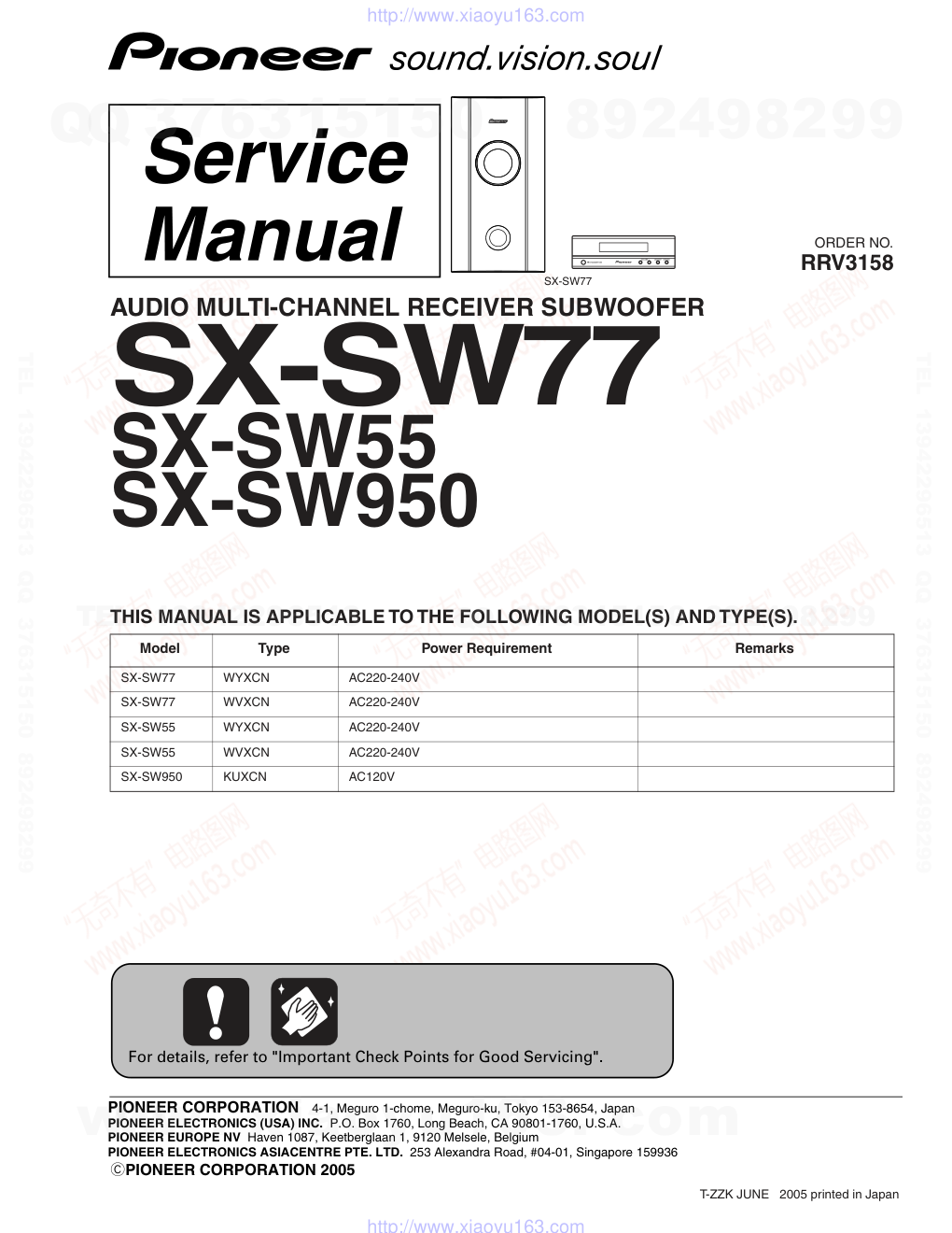
先锋PIONEER SX-SW77电路图
 "先锋PIONEER SX-SW77电路图-0")
 "先锋PIONEER SX-SW77电路图-1")
 "先锋PIONEER SX-SW77电路图-2")
 "先锋PIONEER SX-SW77电路图-3")
 "先锋PIONEER SX-SW77电路图-4")
 "先锋PIONEER SX-SW77电路图-5")
 "先锋PIONEER SX-SW77电路图-6")
 "先锋PIONEER SX-SW77电路图-7")
 "先锋PIONEER SX-SW77电路图-8")
 "先锋PIONEER SX-SW77电路图-9")
ORDER NO. PIONEER CORPORATION 4-1, Meguro 1-chome, Meguro-ku, Tokyo 153-8654, Japan PIONEER ELECTRONICS (USA) INC. P.O. Box 1760, Long Beach, CA 90801-1760, U.S.A. PIONEER EUROPE NV Haven 1087, Keetberglaan 1, 9120 Melsele, Belgium PIONEER ELECTRONICS ASIACENTRE PTE. LTD. 253 Alexandra Road, #04-01, Singapore 159936 PIONEER CORPORATION 2005 STANDBY/ON - VOLUME + AUDIO INPUT SURROUND SX-SW77 RRV3158 AUDIO MULTI-CHANNEL RECEIVER SUBWOOFER SX-SW77 SX-SW55 SX-SW950 THIS MANUAL IS APPLICABLE TO THE FOLLOWING MODEL(S) AND TYPE(S). Model Type Power Requirement Remarks SX-SW77 WYXCN AC220-240V SX-SW77 WVXCN AC220-240V SX-SW55 WYXCN AC220-240V SX-SW55 WVXCN AC220-240V SX-SW950 KUXCN AC120V For details, refer to "Important Check Points for Good Servicing". T-ZZK JUNE 2005 printed in Japan www. xiaoyu163. com QQ 376315150 9 9 2 8 9 4 2 9 8 TEL 13942296513 9 9 2 8 9 4 2 9 8 0 5 1 5 1 3 6 7 3 Q Q TEL 13942296513 QQ 376315150 892498299 TEL 13942296513 QQ 376315150 892498299 http://www.xiaoyu163.com SX-SW77 2 1 2 3 4 1 2 3 4 C D F A B E SAFETY INFORMATION This service manual is intended for qualified service technicians; it is not meant for the casual do-it-yourselfer. Qualified technicians have the necessary test equipment and tools, and have been trained to properly and safely repair complex products such as those covered by this manual. Improperly performed repairs can adversely affect the safety and reliability of the product and may void the warranty. If you are not qualified to perform the repair of this product properly and safely, you should not risk trying to do so and refer the repair to a qualified service technician. WARNING This product contains lead in solder and certain electrical parts contain chemicals which are known to the state of California to cause cancer, birth defects or other reproductive harm. Health & Safety Code Section 25249.6 – Proposition 65 NOTICE (FOR CANADIAN MODEL ONLY) Fuse symbols (fast operating fuse) and/or (slow operating fuse) on PCB indicate that replacement parts must be of identical designation. REMARQUE (POUR MODÈLE CANADIEN SEULEMENT) Les symboles de fusible (fusible de type rapide) et/ou (fusible de type lent) sur CCI indiquent que les pièces de remplacement doivent avoir la même désignation. ANY MEASUREMENTS NOT WITHIN THE LIMITS OUTLINED ABOVE ARE INDICATIVE OF A POTENTIAL SHOCK HAZARD AND MUST BE CORRECTED BEFORE RETURN- ING THE APPLIANCE TO THE CUSTOMER. 2. PRODUCT SAFETY NOTICE Many electrical and mechanical parts in the appliance have special safety related characteristics. These are often not evident from visual inspection nor the protection afforded by them necessarily can be obtained by using replacement components rated for voltage, wattage, etc. Replacement parts which have these special safety characteristics are identified in this Service Manual. Electrical components having such features are identified by marking with a on the schematics and on the parts list in this Service Manual. The use of a substitute replacement component which does not have the same safety characteristics as the PIONEER recommended replacement one, shown in the parts list in this Service Manual, may create shock, fire, or other hazards. Product Safety is continuously under review and new instructions are issued from time to time. For the latest information, always consult the current PIONEER Service Manual. A subscription to, or additional copies of, PIONEER Service Manual may be obtained at a nominal charge from PIONEER. (FOR USA MODEL ONLY) 1. SAFETY PRECAUTIONS The following check should be performed for the continued protection of the customer and service technician. LEAKAGE CURRENT CHECK Measure leakage current to a known earth ground (water pipe, conduit, etc.) by connecting a leakage current tester such as Simpson Model 229-2 or equivalent between the earth ground and all exposed metal parts of the appliance (input/output terminals, screwheads, metal overlays, control shaft, etc.). Plug the AC line cord of the appliance directly into a 120V AC 60 Hz outlet and turn the AC power switch on. Any current measured must not exceed 0.5 mA. Device under test Leakage current tester Earth ground Reading should not be above 0.5 mA Also test with plug reversed (Using AC adapter plug as required) Test all exposed metal surfaces AC Leakage Test www. xiaoyu163. com QQ 376315150 9 9 2 8 9 4 2 9 8 TEL 13942296513 9 9 2 8 9 4 2 9 8 0 5 1 5 1 3 6 7 3 Q Q TEL 13942296513 QQ 376315150 892498299 TEL 13942296513 QQ 376315150 892498299 http://www.xiaoyu163.com SX-SW77 3 5 6 7 8 5 6 7 8 C D F A B E [Important Check Points for Good Servicing] In this manual, procedures that must be performed during repairs are marked with the below symbol. Please be sure to confirm and follow these procedures. 1. Product safety Please conform to product regulations (such as safety and radiation regulations), and maintain a safe servicing environment by following the safety instructions described in this manual. 1 Use specified parts for repair. Use genuine parts. Be sure to use important parts for safety. 2 Do not perform modifications without proper instructions. Please follow the specified safety methods when modification(addition/change of parts) is required due to interferences such as radio/TV interference and foreign noise. 3 Make sure the soldering of repaired locations is properly performed. When you solder while repairing, please be sure that there are no cold solder and other debris. Soldering should be finished with the proper quantity. (Refer to the example) 4 Make sure the screws are tightly fastened. Please be sure that all screws are fastened, and that there are no loose screws. 5 Make sure each connectors are correctly inserted. Please be sure that all connectors are inserted, and that there are no imperfect insertion. 6 Make sure the wiring cables are set to their original state. Please replace the wiring and cables to the original state after repairs. In addition, be sure that there are no pinched wires, etc. 7 Make sure screws and soldering scraps do not remain inside the product. Please check that neither solder debris nor screws remain inside the product. 8 There should be no semi-broken wires, scratches, melting, etc. on the coating of the power cord. Damaged power cords may lead to fire accidents, so please be sure that there are no damages. If you find a damaged power cord, please exchange it with a suitable one. 9 There should be no spark traces or similar marks on the power plug. When spark traces or similar marks are found on the power supply plug, please check the connection and advise on secure connections and suitable usage. Please exchange the power cord if necessary. 0 Safe environment should be secured during servicing. When you perform repairs, please pay attention to static electricity, furniture, household articles, etc. in order to prevent injuries. Please pay attention to your surroundings and repair safely. 2. Adjustments To keep the original performance of the products, optimum adjustments and confirmation of characteristics within specification. Adjustments should be performed in accordance with the procedures/instructions described in this manual. 4. Cleaning For parts that require cleaning, such as optical pickups, tape deck heads, lenses and mirrors used in projection monitors, proper cleaning should be performed to restore their performances. 3. Lubricants, Glues, and Replacement parts Use grease and adhesives that are equal to the specified substance. Make sure the proper amount is applied. 5. Shipping mode and Shipping screws To protect products from damages or failures during transit, the shipping mode should be set or the shipping screws should be installed before shipment. Please be sure to follow this method especially if it is specified in this manual. www. xiaoyu163. com QQ 376315150 9 9 2 8 9 4 2 9 8 TEL 13942296513 9 9 2 8 9 4 2 9 8 0 5 1 5 1 3 6 7 3 Q Q TEL 13942296513 QQ 376315150 892498299 TEL 13942296513 QQ 376315150 892498299 http://www.xiaoyu163.com SX-SW77 4 1 2 3 4 1 2 3 4 C D F A B E CONTENTS SAFETY INFORMATION..................................................................................................................................... 2 1. SPECIFICATIONS ............................................................................................................................................ 4 2. EXPLODED VIEWS AND PARTS LIST ............................................................................................................ 6 2.1 PACKING ................................................................................................................................................... 6 2.2 EXTERIOR................................................................................................................................................. 8 2.3 DISPLAY UNIT......................................................................................................................................... 10 3. BLOCK DIAGRAM AND SCHEMATIC DIAGRAM.......................................................................................... 12 3.1 OVERALL WIRING CONNECTION DIAGRAM AND BLOCK DIAGRAM ................................................ 12 3.2 MAIN ASSY (1/5) ..................................................................................................................................... 14 3.3 MAIN ASSY (2/5) ..................................................................................................................................... 16 3.4 MAIN ASSY (3/5) ..................................................................................................................................... 18 3.5 MAIN ASSY (4/5) ..................................................................................................................................... 20 3.6 MAIN ASSY (5/5) ..................................................................................................................................... 22 3.7 AC INLET, CONNECT and FL ASSYS .................................................................................................... 24 3.8 POWER SUPPLY UNIT............................................................................................................................ 26 3.9 WAVEFORMS .......................................................................................................................................... 28 4. PCB CONNECTION DIAGRAM ..................................................................................................................... 29 4.1 MAIN ASSY ............................................................................................................................................. 30 4.2 AC INLET and CONNECT ASSYS .......................................................................................................... 34 4.3 FL ASSY .................................................................................................................................................. 35 4.4 POWER SUPPLY UNIT............................................................................................................................ 36 5. PCB PARTS LIST ........................................................................................................................................... 38 6. ADJUSTMENT ............................................................................................................................................... 40 7. GENERAL INFORMATION............................................................................................................................. 41 7.1 DIAGNOSIS ............................................................................................................................................. 41 7.1.1 TEST MODE...................................................................................................................................... 41 7.1.2 SPECIFICATIONS OF SPEAKER SETUP ........................................................................................ 43 7.1.3 PROPOSAL OF DSP ERROR DISPLAY........................................................................................... 44 7.1.4 CIRCUIT DESCRIPTION OF DIGITAL AMP. SECTION.................................................................... 45 7.1.5 SPECIFICATIONS FOR THE PROTECTION CIRCUITS FOR THE DIGITAL AMPLIFIER............... 46 7.1.6 CONDITIONS FOR SWITCHING THE ROTATION SPEED OF THE FAN ........................................ 47 7.1.7 DISASSEMBLY.................................................................................................................................. 48 7.2 IC ............................................................................................................................................................. 51 8. PANEL FACILITIES ........................................................................................................................................ 67 1. SPECIFICATIONS • Amplifier section RMS Power Output : SX-SW950 Front, Center, Surround (1 kHz, 10 % THD, 6 Ω) Subwoofer . . . . . . . . . . . . FTC Power Output : Front, Center, Surround (200 Hz, - 20 kHz 1 % THD, 6 Ω) Subwoofer. . . . . . . 50 W (45 Hz - 200 Hz, 1 % THD, 6 Ω) • FM tuner section Frequency range . . . . . . . . . . . . . . . . 87.5 MHz to 108 MHz Antenna. . . . . . . . . . . . . . . . . . . . . . . . . . . 75 Ω, unbalanced • AM tuner section Frequency range . . . . . . . . . . . . . . . . 530 kHz to 1,700 kHz Antenna . . . . . . . . . . . . . . . . . . . . . . . . . . . . . Loop antenna • Subwoofer section Enclosure. . . . . . . . . . . . . . . . . . . . . . . .Bass-reflex floor type (magnetically shielded) System . . . . . . . . . . . . . . . . . . . . . . . . . 16 cm 1-way system Speaker . . . . . . . . . . . . . . . . . . . . . . . . . . . 16 cm cone type Nominal impedance . . . . . . . . . . . . . . . . . . . . . . . . . . . . 6 Ω Frequency range . . . . . . . . . . . . . . . . . . . . 25 Hz to 1.0 kHz Maximum Input Power . . . . . . . . . . . . . . . . . . . . . . . . 60 W • Miscellaneous Power requirements. . . . . . . . . . . . . . . . AC 120 V, 50/60 Hz Power consumption. . . . . . . . . . . . . . . . . . . . . . . . . . . . 47 W Power consumption in standby . . . . . . . . . . . . . . . . . . 0.2 W Dimensions . . . . . 7 7 / 8 (W) x 14 3 / 4(H) x 17 3 / 16 (D) in. 200 (W) x 375 (H) x 437 (D) mm Weight . . . . . . . . . . . . . . . . . . . . . . . . . . . . . . . 19 lb. 13 oz. 9.0 kg • Accessories Remote control. . . . . . . . . . . . . . . . . . . . . . . . . . . . . . . . . . . 1 Display unit . . . . . . . . . . . . . . . . . . . . . . . . . . . . . . . . . . . . 1 AA/R6 dry cell batteries . . . . . . . . . . . . . . . . . . . . . . . . . . . 2 Coaxial cable . . . . . . . . . . . . . . . . . . . . . . . . . . . . . . . . . . . 1 Display cable . . . . . . . . . . . . . . . . . . . . . . . . . . . . . . . . . . . 1 AM loop antenna . . . . . . . . . . . . . . . . . . . . . . . . . . . . . . . . 1 FM wire antenna . . . . . . . . . . . . . . . . . . . . . . . . . . . . . . . . . 1 Power cord . . . . . . . . . . . . . . . . . . . . . . . . . . . . . . . . . . . . . 1 Warranty card . . . . . . . . . . . . . . . . . . . . . . . . . . . . . . . . . . . 1 Operating instructions 60 W per channel 60 W (200 Hz, 10 % THD, 6 Ω) 50 W per channel . . . . . . . . . . . . . . . . . . . . . . . . www. xiaoyu163. com QQ 376315150 9 9 2 8 9 4 2 9 8 TEL 13942296513 9 9 2 8 9 4 2 9 8 0 5 1 5 1 3 6 7 3 Q Q TEL 13942296513 QQ 376315150 892498299 TEL 13942296513 QQ 376315150 892498299 http://www.xiaoyu163.com SX-SW77 5 5 6 7 8 5 6 7 8 C D F A B E • Amplifier section RMS Power Output : Front, Center, Surround . . . . . . . . . . . . .110 W per channel (1 kHz, 10 % T.H.D., 3Ω) Subwoofer . . . . . . . . . . . . . 70 W (200 Hz, 10 % T.H.D., 3Ω) Front, Center, Surround . . . . . . . . . . . . .60 W per channel (1 kHz, 10 % T.H.D., 6Ω) Subwoofer. . . . . . . . . . . . 60 W (200 Hz, 10 % T.H.D., 6Ω) • FM tuner section Frequency range . . . . . . . . . . . . . . . . 87.5 MHz to 108 MHz Antenna. . . . . . . . . . . . . . . . . . . . . . . . . . . 75Ω, unbalanced • AM tuner section Frequency range. . . . . . . . . . . . . . . . . 531 kHz to 1,602 kHz Antenna. . . . . . . . . . . . . . . . . . . . . . . . . . . . . . Loop antenna • Subwoofer section Enclosure . . . . . . . . . . . . . . . . . . . . . . .Bass-reflex floor type (magnetically shielded) System. . . . . . . . . . . . . . . . . . . . . . . . . .16 cm 1-way system Speaker . . . . . . . . . . . . . . . . . . . . . . . . . . . .16 cm cone type Nominal impedance. . . . . . . . . . . . . . . . . . . . . . . . . . . . . . 6Ω Frequency range . . . . . . . . . . . . . . . . . . . . 25 Hz to 1.0 kHz Maximum Input Power . . . . . . . . . . . . . . . . . . . . . . . . . 60 W • Miscellaneous Power requirements. . . . . . . . . . . . AC 220-240 V, 50/60 Hz Power consumption. . . . . . . . . . . . . . . . . . . . . . . . . . . .51 W Power consumption in standby . . . . . . . . . . . . . . . . . . 0.4 W Dimensions. . . . . . . . . . . . . 200 (W) x 375 (H) x 437 (D) mm Weight. . . . . . . . . . . . . . . . . . . . . . . . . . . . . . . . . . . . . 9.0 kg • Accessories Remote control. . . . . . . . . . . . . . . . . . . . . . . . . . . . . . . . . . .1 Display unit. . . . . . . . . . . . . . . . . . . . . . . . . . . . . . . . . . . . . .1 AA/R6 dry cell batteries. . . . . . . . . . . . . . . . . . . . . . . . . . . . 2 Audio cable (red/white) . . . . . . . . . . . . . . . . . . . . . . . . . . . . 1 Optical cable. . . . . . . . . . . . . . . . . . . . . . . . . . . . . . . . . . . . .1 Control cable . . . . . . . . . . . . . . . . . . . . . . . . . . . . . . . . . . . .1 Display cable . . . . . . . . . . . . . . . . . . . . . . . . . . . . . . . . . . . .1 AM loop antenna . . . . . . . . . . . . . . . . . . . . . . . . . . . . . . . . .1 FM wire antenna . . . . . . . . . . . . . . . . . . . . . . . . . . . . . . . . . 1 Power cord . . . . . . . . . . . . . . . . . . . . . . . . . . . . . . . . . . . . . 1 Warranty card. . . . . . . . . . . . . . . . . . . . . . . . . . . . . . . . . . . .1 Operating instructions Remote control (SX-SW77 : AXD7417) (SX-SW55 /WYXCN : AXD7419) (SX-SW55 /WVXCN : AXD7420) (SX-SW950 : AXD7425) Note • Specifications and design subject to possible modification without notice, due to improvements. Manufactured under license from Dolby Laboratories."Dolby", "Pro Logic" and the double-D symbol are trademarks of Dolby Laboratories. "DTS" and "DTS Digital Surround" are registered trademarks of Digital Theater Systems, Inc. SYSTEM CONNECTOR SPEAKERS DVD/DVR 2 (OPTICAL) AC IN CENTER SURROUND DVD/DVR 1 (COAXIAL) DIGITAL AUDIO INPUT ANTENNA FM UNBAL75Ω AM LOOP ANTENNA ANALOG DIGITAL (OPTICAL) R L R L FRONT R L CONTROL OUTSUB WOOFER USE ONLY WITH DISPLAY UNIT DIGITAL OUT CONTROL G-LINK IN OPTICAL AV 1 (RGB) - TV AV 2 (INPUT 1/DECODER) S-VIDEO VIDEO AUDIO L R COMPONENT VIDEO OUT Y PB PR ANTENNA IN OUT AC IN OUTPUT S-VIDEO VIDEO AUDIO L R INPUT 3 AM loop antenna (ATB7013) Display unit Receiver subwoofer (SX-SW77) Display cable (ADE7113) FM antenna (ADH7030) DVD Recorder (DVR-530H-AV) Optical cable (ADE7116) Control cable (ADE7114) Audio cable (red/white) (ADE7117) VOLUME + – MUTE RECORDER RECEIVER TOP MENU RDS DISP SYSTEM SETUP DISPLAY TEST TONE ST + ST - TUNE + TUNE - RETURN DISC NAVIGATOR DVD MENU HOME MENU AUDIO SURROUND ADVANCED SOUND TIMER REC SUBTITLE ANGLE PLAY MODE SHIFT VIDEO INPUT INFO GUIDE HDD DVD FM/AM AUDIO INPUT HELP TV/DVD TV DIRECT REC INPUT TV ENTER CLEAR TV CONTROL CHANNEL VOLUME REC PREV NEXT STEP/SLOW STOP REC REC MODE ONE TOUCH COPY CHANNEL � � � � � � SKIP CM BACK SX-SW77 www. xiaoyu163. com QQ 376315150 9 9 2 8 9 4 2 9 8 TEL 13942296513 9 9 2 8 9 4 2 9 8 0 5 1 5 1 3 6 7 3 Q Q TEL 13942296513 QQ 376315150 892498299 TEL 13942296513 QQ 376315150 892498299 http://www.xiaoyu163.com SX-SW77 6 1 2 3 4 1 2 3 4 C D F A B E 2. EXPLODED VIEWS AND PARTS LIST 2.1 PACKING Parts marked by "NSP" are generally unavailable because they are not in our Master Spare Parts List. The mark found on some component parts indicates the importance of the safety factor of the part. Therefore, when replacing, be sure to use parts of identical designation. Screws adjacent to mark on product are used for disassembly. For the applying amount of lubricants or glue, follow the instructions in this manual. (In the case of no amount instructions, apply as you think it appropriate.) NOTES: 8 7 6 4 SX-SW77 only SX-SW77 only SX-SW55, SX-SW950 only SX-SW77, SX-SW55 only WVXCN, KUXCN only WYXCN, WVXCN only 2 5 3 1 11 12 22 22 22 10 9 24 (2/2) 24 (1/2) 13 27 28 23 26 22 15 16 17 18 19 21 20 25 (2/2) 25 (1/2) WYXCN, KUXCN only WYXCN only WYXCN only For WVXCN type 6 www. xiaoyu163. com QQ 376315150 9 9 2 8 9 4 2 9 8 TEL 13942296513 9 9 2 8 9 4 2 9 8 0 5 1 5 1 3 6 7 3 Q Q TEL 13942296513 QQ 376315150 892498299 TEL 13942296513 QQ 376315150 892498299 http://www.xiaoyu163.com SX-SW77 7 5 6 7 8 5 6 7 8 C D F A B E (1) PACKING SECTION PARTS LIST (2) CONTRAST TABLE SX-SW77/WYXCN, WVXCN, SX-SW55/WYXCN, WVXCN and SX-SW950/KUXCN are constructed the same except for the following: Mark No. Description Part No. 1 Display Cable ADE7113 2 Control Cable See Contrast table (2) 3 Optical Cable See Contrast table (2) 4 Audio Cable (red/white) See Contrast table (2) 5 Coaxial Cord See Contrast table (2) > 6 AC Power Cord See Contrast table (2) 7 FM Wire Antenna ADH7030 8 AM Loop Antenna ATB7013 9 Remote Control Unit See Contrast table (2) 10 Battery Cover AZA7424 NSP 11 Dry Cell Battery (R6P, AA) VEM1010 12 DISPLAY Unit See Contrast table (2) 13 Operating Instructions See Contrast table (2) (Enslish) 14 • • • • • • 15 Operating Instructions See Contrast table (2) (German) 16 Operating Instructions See Contrast table (2) (Spanish) 17 Operating Instructions See Contrast table (2) (French) 18 Operating Instructions See Contrast table (2) (Italian) 19 Operating Instructions See Contrast table (2) (Dutch) 20 Label (WEEE) See Contrast table (2) NSP 21 Warranty Card See Contrast table (2) NSP 22 Polyethylene Bag Z21-038 NSP 23 Polyethylene Bag AHG7126 24 Pad T AHA7448 25 Pad B AHA7449 26 Packing Case SW See Contrast table (2) 27 Packing Sheet AHG7125 28 Packing Sheet L AHG7128 Mark No. Description Part No. Mark No. Symbol and Description SX-SW77/ WYXCN SX-SW77/ WVXCN SX-SW55/ WYXCN SX-SW55/ WVXCN SX-SW950/ KUXCN 2 Cord with Mini Plug ADE7114 ADE7114 ADE7114 ADE7114 Not used 3 Optical Fiber Cable ADE7116 ADE7116 Not used Not used Not used 4 Cord with Plug ADE7117 ADE7117 Not used Not used Not used 5 Coaxial Cord Not used Not used ADE7115 ADE7115 ADE7115 > 6 AC Power Cord ADG1154 ADG1156 ADG1154 ADG1156 ADG7022 9 Remote Control Unit AXD7417 AXD7417 AXD7419 AXD7420 AXD7425 12 DISPLAY Unit AXX7204 AXX7204 AXX7204 AXX7204 Not used NSP 12 DISPLAY Unit Not used Not used Not used Not used AXX7205 13 Operating Instructions (English) Not used ARB7342 Not used ARB7343 ARE7385 15 Operating Instructions (German) ARC7636 Not used ARC7638 Not used Not used 16 Operating Instructions (Spanish) ARC7637 Not used ARC7639 Not used Not used 17 Operating Instructions (French) ARC7646 Not used ARC7649 Not used Not used 18 Operating Instructions (Italian) ARC7647 Not used ARC7650 Not used Not used 19 Operating Instructions (Dutch) ARC7648 Not used ARC7651 Not used Not used 20 Label (WEEE) ARW7322 ARW7322 ARW7322 ARW7322 Not used NSP 21 Warranty Card ARY7065 ARY7065 ARY7065 ARY7065 ARY7045 26 Packing Case SW AHD8375 AHD8375 AHD8381 AHD8381 AHD8392 www. xiaoyu163. com QQ 376315150 9 9 2 8 9 4 2 9 8 TEL 13942296513 9 9 2 8 9 4 2 9 8 0 5 1 5 1 3 6 7 3 Q Q TEL 13942296513 QQ 376315150 892498299 TEL 13942296513 QQ 376315150 892498299 http://www.xiaoyu163.com SX-SW77 8 1 2 3 4 1 2 3 4 C D F A B E 2.2 EXTERIOR A A B B A F B E CONTACT SIDE NON-CONTACT SIDE 38 37 6 10 36 39 39 18 39 40 39 39 39 39 39 39 39 12 19 28 19 22 21 9 27 2 7 8 1 11 15 16 4 5 13 30 25 23 24 31 20 29 26 39 39 39 39 39 39 14 39 17 39 3 39 Cleaning paper GED-008 www. xiaoyu163. com QQ 376315150 9 9 2 8 9 4 2 9 8 TEL 13942296513 9 9 2 8 9 4 2 9 8 0 5 1 5 1 3 6 7 3 Q Q TEL 13942296513 QQ 376315150 892498299 TEL 13942296513 QQ 376315150 892498299 http://www.xiaoyu163.com SX-SW77 9 5 6 7 8 5 6 7 8 C D F A B E (1) EXTERIOR SECTION PARTS LIST (2) CONTRAST TABLE SX-SW77/WYXCN, WVXCN, SX-SW55/WYXCN, WVXCN and SX-SW950/KUXCN are constructed the same except for the following: Mark No. Description Part No. 1 MAIN Assy See Contrast table (2) 2 AC INLET Assy See Contrast table (2) > 3 POWER SUPPLY Unit AWR7037 4 FM/AM TUNER Unit See Contrast table (2) 5 11P Flexible Cable ADD7506 6 Connecting Cord ADX7484 7 2P Lead with Housing ADX7485 8 11P Lead with Housing ADX7486 9 2P Lead with Housing ADX7487 10 Speaker A14LR75-51D 11 DC Fan Motor VXM1121 NSP 12 Chassis B ANA7179 NSP 13 Chassis T ANA7180 14 Rear Panel SW See Contrast table (2) 15 Screw (3 x 11.5) ABA7129 16 Rubber Bushing AEB7369 17 Cushion F AEB7370 18 Cushion TX AEB7371 19 Rivet AEC7514 20 Packing AEC7548 NSP 21 Barrier SW AEC7552 NSP 22 Barrier AC AEC7553 NSP 23 Duct Ring AMR7511 NSP 24 Paper Tube 60 AMR7512 NSP 25 Acoustic Absorbent AMV7001 NSP 26 Mesh ANC8354 NSP 27 Ferrite Clamp DTH1158 NSP 28 PCB Holder PNW2029 NSP 29 Cosmetic Baffle See Contrast table (2) NSP 30 Cabinet AMM7009 31 Pioneer Name Plate VAM1152 32 Baffle Assy See Contrast table (2) 33 • • • • • 34 • • • • • 35 • • • • • 36 Screw BBZ40P120FNI 37 Screw BYC40P160FNI 38 Screw BYC40P200FNI 39 Screw PBZ30P080FTC 40 Screw PSZ30P060FNI Mark No. Description Part No. Mark No. Symbol and Description SX-SW77/ WYXCN SX-SW77/ WVXCN SX-SW55/ WYXCN SX-SW55/ WVXCN SX-SW950/ KUXCN 1 MAIN Assy AWK7883 AWK7883 AWK7883 AWK7883 AWK7884 2 AC INLET Assy AWU8273 AWU8273 AWU8273 AWU8273 AWU8274 4 FM/AM TUNER Unit AXX7170 AXX7170 AXX7170 AXX7170 AXX7172 14 Rear Panel SW ANC8323 ANC8323 ANC8356 ANC8356 ANC8362 NSP 29 Cosmetic Baffle AMB7903 AMB7903 AMB7903 AMB7903 AMB7905 32 Baffle Assy AXG7278 AXG7278 AXG7278 AXG7278 AXG7279 www. xiaoyu163. com QQ 376315150 9 9 2 8 9 4 2 9 8 TEL 13942296513 9 9 2 8 9 4 2 9 8 0 5 1 5 1 3 6 7 3 Q Q TEL 13942296513 QQ 376315150 892498299 TEL 13942296513 QQ 376315150 892498299 http://www.xiaoyu163.com SX-SW77 10 1 2 3 4 1 2 3 4 C D F A B E 2.3 DISPLAY UNIT D C 11 10 10 7 3 1 2 5 8 (1/2) 9 4 12 6 8 (2/2) www. xiaoyu163. com QQ 376315150 9 9 2 8 9 4 2 9 8 TEL 13942296513 9 9 2 8 9 4 2 9 8 0 5 1 5 1 3 6 7 3 Q Q TEL 13942296513 QQ 376315150 892498299 TEL 13942296513 QQ 376315150 892498299 http://www.xiaoyu163.com SX-SW77 11 5 6 7 8 5 6 7 8 C D F A B E (1) DISPLAY UNIT PARTS LIST (2) CONTRAST TABLE SX-SW77/WYXCN, WVXCN, SX-SW55/WYXCN, WVXCN and SX-SW950/KUXCN are constructed the same except for the following: Mark No. Description Part No. 1 FL Assy AWU8271 2 CONNECT Assy AWU8272 3 Leg AEB7368 4 Window AAK8285 5 FL Filter AEC7535 6 Display Panel AMB7899 7 Display Cover AMC7059 8 PWR Button Assy AXG7260 9 Pioneer Name Plate VAM1152 10 Screw BPZ30P080FNI 11 Screw PSZ30P060FNI 12 DISPLAY Unit See Contrast table (2) Mark No. Symbol and Description SX-SW77/ WYXCN SX-SW77/ WVXCN SX-SW55/ WYXCN SX-SW55/ WVXCN SX-SW950/ KUXCN 12 DISPLAY Unit AXX7204 AXX7204 AXX7204 AXX7204 Not used NSP 12 DISPLAY Unit Not used Not used Not used Not used AXX7205 www. xiaoyu163. com QQ 376315150 9 9 2 8 9 4 2 9 8 TEL 13942296513 9 9 2 8 9 4 2 9 8 0 5 1 5 1 3 6 7 3 Q Q TEL 13942296513 QQ 376315150 892498299 TEL 13942296513 QQ 376315150 892498299 http://www.xiaoyu163.com SX-SW77 12 1 2 3 4 1 2 3 4 C D F A B E 3. BLOCK DIAGRAM AND SCHEMATIC DIAGRAM 3.1 OVERALL WIRING CONNECTION DIAGRAM AND BLOCK DIAGRAM 1 2 3 4 7 8 5 6 9 11 10 2 1 11 9 10 7 8 5 6 2 3 4 1 AN1 CN5 CN5701 3001 CN3201 CN1001 CN5602 B2P3S-VH B2P3S-VH B2P-VH B11B-PH-K-S 9604S-11C (SX-SW950 AUX) B2P-VH B11B-PH-K-S B2B-PH-K-S KUXCN:XKP3085 WYXCN,WVXCN:XKP3084 AC CORD NEUTRAL LIVE WYXCN,WVXCN:AWU8273 KUXCN:AWU8274 AC INLET ASSY LIVE NEUTRAL ADX7487 +B GND VFDP FL DC+ FL DC- GNDD POWER CONT VS+3R3 GND (AWR7037) SW POWER SUPPLY VE+5 BEAT CUT VS+12 VSF+12 KUXCN:AXX7172 WYXCN, WVXCN:AXX7170 TUNER MODULE 11pin FFC ADD7506 ANALOG INPUT ADX7485 VSM TXR +9V TXL GND CLK DI CE DO RDS BU1924FS ADX7486 GND RDS INPUT SELECTOR PCM1803DB FAN+ GNDF A/D CONVERTER MCLK RDSDATA,RDSCLK,RDSPOW XADPDN ADDATA INPUTSELA FAN VXM1121 4 10 IC5701 IC3001 IC3003 TC4052BFN TX 5 14 1 12 3 13 1 7 15 12 2 ANALOG AUDIO SIGNAL DIGITAL or PWM AUDIO SIGNAL COMMUNICATION LINE 2 1 2 1 11 9 10 6 8 5 7 1 4 3 2 2 1 2 1 1 2 3 4 8 6 9 11 10 7 5 2 1 9 2 16 E B F www. xiaoyu163. com QQ 376315150 9 9 2 8 9 4 2 9 8 TEL 13942296513 9 9 2 8 9 4 2 9 8 0 5 1 5 1 3 6 7 3 Q Q TEL 13942296513 QQ 376315150 892498299 TEL 13942296513 QQ 376315150 892498299 http://www.xiaoyu163.com SX-SW77 13 5 6 7 8 5 6 7 8 C D F A B E 9 10 7 8 13 11 12 3 2 1 4 6 7 5 11 12 9 6 2 4 3 8 7 10 1 5 3 5 6 2 4 1 9 10 8 13 11 12 4 3 1 2 10 6 7 5 11 12 9 8 JA4603 JA4602 JA4601 CN5901 CN5651 JA5951 CN5652 CN5601 GP1FAV51RKBF GP1FAV51RKBF VKB1159 XKP3077 XKP3066 RKN1004 AKP7131 AKP7131 VOL+ VOL- STANDBY/ON FL TUBE SELECTOR SURROUND INPUT FL DRIVER KEY2 GNDS GNDD KEY1 VFDP REMOCON GNDS 12.F- 11.F+ ADE7113 (AWU8271) FL ASSY (OPT) (COAX) (OPT) DIGITAL DVD/DVR2 DVD/DVR1 PC/GAME SX-SW950 DTV DVD DIGITAL INPUT IR VE+5 XFLCS FLCK FLDATA FLDC- FLDC+ (AWU8272) CONNECT ASSY SR OUT SW C - AKE7116 CN3211 - - SELECTOR AK4117VF DIR POWER IC TAS5112ADCA POWER IC TAS5112ADCA DSPC56371AF180 TAS5508APAG PWM PROCESSOR DIGITAL AUDIO 5V -> 3V MAIN ASSY FDTI PWM7.8 PWM2.4 PWM1.3 DIGSEL DSP u-COM WYXCN,WVXCN:AWK7883 KUXCN:AWK7884 5.FLDATA 6.REMOCON 7.XFLCS 8.FLCK 9.VE+5 10.KEY1 1.GNDD 2.GNDD 3.VFDP 4.KEY2 SR FR SL - - - FL TAS5112ADCA POWER IC IR FLDAT KEY&IR SHUTDOWN/XOTW DASDA,DASCL,XDAPDN,DSPMUTE DIRDO,DIRERR IC4602 TC74VHC00FTS1 75 76 49 74 14 13 12 3 5 8 2 5 1 73 63 37 IC5501 IC3101 IC3401 IC3301 IC3201 PDC128A IC951 TC74VHC08FTS1 IC601 IC801 4 12 77 79 67 100 5 6 7 27 28 35 71 7 19 69 6 64 65 29 30 31 23-25 23-25 23-25 S5961 S5962 S5963 S5964 S5965 IC5902 IC5901 PT6315 V5901 AAV7104 GP1UM27XK0VF + + + + + + 50 51 34 35 34 35 34 35 50 51 50 51 46 47 38 39 38 39 38 39 46 47 46 47 14 13 24 25 17 22 D C A ÷ When ordering service parts, be sure to refer to "EXPLODED VIEWS and PARTS LIST" or "PCB PARTS LIST". ÷ The > mark found on some component parts indicates the importance of the safety factor of the part. Therefore, when replacing, be sure to use parts of identical designation. ÷ : The power supply is shown with the marked box. www. xiaoyu163. com QQ 376315150 9 9 2 8 9 4 2 9 8 TEL 13942296513 9 9 2 8 9 4 2 9 8 0 5 1 5 1 3 6 7 3 Q Q TEL 13942296513 QQ 376315150 892498299 TEL 13942296513 QQ 376315150 892498299 http://www.xiaoyu163.com SX-SW77 14 1 2 3 4 1 2 3 4 C D F A B E 3.2 MAIN ASSY (1/5) LC875BJ0A PDC128A 49 DSPMUTE 72 35 33 19 69 RMC 51 50 22 UCOM 67 DSP 28 27 25 23 24 22 21 19 7 6 35 33 37 45 38 46 49 50 52 86 51 96 87 61 65 62 64 66 69 70 71 72 77 75 79 74 76 99 100 98 94 96 87 85 84 86 C2 E2 1 2 4 3 E B C B2 1 2 3 E C B C E C2 E2 B2 C E B C2 E B 7 5 10 6 8 11 12 9 E B C E2 B2 C B 3 1 2 32 31 34 35 33 28 29 30 27 26 39 37 38 36 40 41 42 45 43 44 46 47 48 49 50 53 52 51 54 55 24 25 23 22 21 20 57 56 58 59 61 60 18 19 17 16 15 14 13 62 63 64 66 65 68 67 12 11 10 9 7 8 69 70 71 72 73 74 5 6 4 3 2 1 76 75 78 77 79 80 1 2 3 5 4 82 81 83 85 84 89 88 87 86 90 91 92 93 95 94 98 97 96 99 100 1 C5608 C5601 D5601 D5602 C5602 C5603 D5604 C5604 D5603 C5609 D5605 R5529 Q5501 R5526 R5527 Q5503 Q5504 R5528 Q5501 Q5503 Q5502 D5501 R5531 D1410 R1404 R1406 R1403 R1402 C5607 CN5601 C5606 C5605 R1416 Q5525 C5525 C5524 R5524 R5525 C5526 C5523 C5521 C5522 R5523 R5522 R5521 R5515 R5516 R5514 R5513 R5517 C5519 R5519 C5508 R5508 X5501 C5509 R5507 R5506 C5507 R5503 R5504 R5501 R5502 C1415 D1415 C1413 Q1410 D1412 R1411 Q1410 D1402 Q1413 R1415 R5543 R5544 Q1401 D1401 R1405 R1407 R1401 Q1402 R5530 R5532 R5535 R5536 R5537 C5539 R5549 C5556 R5557 R5511 IC5501 C5518 C5577 R5561 R5562 R5567 R5518 R5520 R5570 R5573 R5578 R5579 R5577 R5505 IC5502 R5595 R5594 R5596 R5597 R5613 C5579 R5583 R5581 R5582 C5581 C5582 R5584 R5580 KN5501 R5574 R5575 10.KEY1 11.F+ 12.F- 9.VE+5 8.FLCK 7.XFLCS 6.REMOCON 3.VFDP 1.GNDD 2.GNDD 5.FLDATA 4.KEY2 CHASSIS FLDAT KEY2 (1/2) (1/2) (2/2) (2/2) DSP MUTE XDAMUTE ADMD XDSPMUTE XPROTECT KEY1 XFLCS FLCLK DIRERR STBY DESTINATION MODEL (2/2) (1/2) PROTECT STBY TEST POINT UTEST STEST SHORT for NC NC XDSPMUTE DASDA DASCK (LED) XDEC MUTE DSPHREQ VSS4 NC VDD4 NC STEST UTEST XDSPSS XDSPRST FLCLK TXCE NC NC NC DSPCK NC DSPDI DSPDO NC PCONFIG XPROTECT NC NC FLDAT NC NC ADMD XFLCS VDD2 VSS2 EEP_CS EEP_DO EEP_SK TXCLK NC NC KEY2 NC MODEL VDD1 SIMUKE µ-COM TXODATA NC RDSPOW RDSDATA DIRERR TXIDATA CF2 CF1 XT2 VSS1 REMOCON XT1 XRESET DIRDO XDIRCS XDIRRST (DTSMIX) (PWRERR) (PWRCONT1) PWRCONT2 EEP_DI KEY1 XDARST XDAPDN (FREQCONT2) (PSVC) XDAMUTE P_ON RDSCLK NC PDNDET (DMUTECHECK) FANCONT NC NC FLASHCLK FLASHDO FLASHE/D (SWMIX) TXPOWER VSS3 VDD3 BEATCUT2 BEATCUT1 XADPDN INPUTSELA DIGSEL SHUTDWN (DC DET) FLCONT (FREQCONT1) XOTW RESET CHASSIS GND GNDD VFDP STBY 100p 100p 100p UDZS8R2(B) 100p UDZS8R2(B) 100p UDZS8R2(B) CH UDZS8R2(B) CH CH UDZS8R2(B) CH CH UMD2N DTA124EUA UMD2N 10k 10k 10k UMD2N UMD2N DAP202K DTC124EUA VFDP 220 10k UDZS15(B) 10k 12k 10k 47k VFLDC- AKP7131 STBY STBY STBY STBY VFLDC+ GNDD VE+5 VS+5 VE+5 DTC143EUA STBY 10/50 47k VU+5 RAB4C221J 220 CH 100p CH 100p 0.01 STBY STBY 220 220 * * 10k 0.01 220 STBY * VE+5 * 2.2k 0.01 ASS7034 10MHz VU+5 0 STBY 10k STBY STBY STBY UDZS4R7(B) STBY UMD2N 1SS355 UMD2N 10k DAN202K 2SA1576A(QR) DTC124EUA 10k 10k 10k VS+3R3 2SA1576A(QR) 4.7k 10k 15k 1SS355 VS+12 VS+5 220 220 RAB4C221J 0.1/16 220 220 220 GNDD 220 RAB4C221J 0.1/16 220 RAB4C221J 0.1/16 0.01 220 220 220 0.01 0.01 1k 220 RAB4C221J 220 220 10k RAB4C221J 220 220 RAB4C221J STBY 220 STBY VU+5 PST3245 220 220 220 220 STBY 220 RAB4C221J 100/16 STBY STBY STBY 220 RAB4C221J STBY 0.1/16 VNF1109 10k VE+5 10k VS+3R3 R5592 A 1/5 CN5652 C www. xiaoyu163. com QQ 376315150 9 9 2 8 9 4 2 9 8 TEL 13942296513 9 9 2 8 9 4 2 9 8 0 5 1 5 1 3 6 7 3 Q Q TEL 13942296513 QQ 376315150 892498299 TEL 13942296513 QQ 376315150 892498299 http://www.xiaoyu163.com SX-SW77 15 5 6 7 8 5 6 7 8 C D F A B E 2/5-5/5 3/5 A A DSP UCOM 85 84 RMC 7 67 1 11 10 B2 E2 C2 E2 C B E B2 C2 B 4 3 C 5 6 1 2 8 7 E B 9 7 8 6 5 3 4 2 1 E 2 1 C 1 3 2 B C E R5607 Q5601 R5602 R5605 R5603 Q5603 R5608 Q5602 R5604 KN1001 C1203 C1505 C1501 L1501 R5606 R5601 Q1301 C1502 D1501 Q5604 D1301 R1302 R1301 R5612 C5610 R5553 C5549 Q1301 Q5604 D5608 D5607 R5806 R5805 C5550 D5801 Q5804 IC5503 R5554 R5804 Q5803 R5803 R5801 Q5951 R5953 R5611 CN1001 D5609 D5606 R5614 R5609 R5610 R5802 CN5602 Q5801 R5955 JA5951 C5951 L5951 D5951 D5952 R5952 Q5952 R5951 R5954 FLCONT FL CHASSIS GND VFDP FL DC+ PWRCONT2 Modulator µcom STBY (2/2) (2/2) FL DRIVER SUPPLY POWER DO DI µcom SR (1/2) TEST GND CS SK REMOCON VCC NC VS+3R3 POWER CONT FL DC- GNDD GNDD VE+5 BEAT CUT VS+12 VSF+12 (1/2) AUDIO BUFFER INPUT SELECTOR TUNER GNDF FAN + BEAT CUT (others : RS1/16S***J(1608size) All Resistors are in k-k Ω, M-M Ω or Ω (others : CEAT) JQ : CEJQ 1/8W : RS1/8S***J(3216size) 1/10W : RS1/10S***J(2125size) MODEL ALL 47k 47k * * R5516 R5514 R5515 R5513 SR OUT SR OUT 47k * * Destination WY,WV KU otherwise specified Rated Voltage : 50V unless CH : CCSRCH(1608size) (others : CKSRYB(1608size)) SQ : CKSQ**(2125size) unless otherwise specified All Capacitors are in p-pF or uF Ratings : Capacity(uF)/Voltage(V) NOTES 4-C1 3-D2 VFDP VFLDC+ VFLDC- STBY 0 2SA1602A(EF) GNDD 6.8k 680 100k 2SC4081(QR) 100k 0 2SA1602A(EF) GNDD GNDF STBY VNF1109 100/16 STBY VS+3R3 22uH LFEA220J VU+5 0.1/16 0.01 STBY UMF21N UMF21N 1SS355 VE+5 1/10W 560 47k GNDF 100/16 47k 47p CH VS+5 UMF21N UMF21N 1SS355 1SS355 UDZS3R9(B) VSFAN GNDD 22k GNDD 0.1/16 2SC4081(QR) 1SS355 1k VE+5 47k BR93L46RFJ-W GNDD 2SC4081(QR) 22k 22k 22k VS+12 DTC124EUA 10k 1SS355 1k 3.3k 47k B11B-PH-K-S 1SS355 560 VSF+12 560 560 VS+12 GNDF B2B-PH-K-S VSFAN 150 2SA1576A(QR) VS+12 3.9k RKN1004 STBY QTL1013 1SS355 2SA1576A(QR) 4.7k 100k VE+5 A 1/5 A 1/5 MAIN ASSY CN3 E (WYXCN,WVXCN:AWK7883) (KUXCN:AWK7884) 12.03 5.08 3.31 5.06 4.98 -25.30 -19.10 -22.70 EEPROM FAN FAN (VXM1121) POWER VSF+12 VSF+12 VSF+12 VSFAN VSFAN VSFAN 12.3 13.1 7.4 13.0 12.2 6.7 LOW ROTATION FAN VOLTAGE TABLE FAN VOLTAGE TABLE FAN VOLTAGE TABLE LOW HIGH Analog IN (VOL19 or less) VOL20 or more Not Digital Stream. (The Analog IN is excluded) VOLTAGE Reference voltage value • It will be described in . • It may fluctuate by the product. www. xiaoyu163. com QQ 376315150 9 9 2 8 9 4 2 9 8 TEL 13942296513 9 9 2 8 9 4 2 9 8 0 5 1 5 1 3 6 7 3 Q Q TEL 13942296513 QQ 376315150 892498299 TEL 13942296513 QQ 376315150 892498299 http://www.xiaoyu163.com SX-SW77 16 1 2 3 4 1 2 3 4 C D F A B E 3.3 MAIN ASSY (2/5) + - + - UCOM 66 62 61 52 75 65 6 64 11 10 8 9 7 5 6 4 3 7 8 6 4 5 3 2 1 9 11 10 14 12 13 16 15 1 2 1 C E B 9 10 13 12 11 15 14 16 7 8 5 6 4 3 1 2 1 8 3 4 2 3 2 5 4 6 7 8 C5705 C5704 C5701 C5702 C5703 C5709 R5719 C5707 R5705 C5708 D5701 R5718 R5717 Q5703 R5708 R5707 C5716 C5706 R5706 C5713 Q5701 R5704 R5703 C5719 R5710 IC5701 C5715 C5720 X5701 C5714 C5712 CN5701 R5712 R5711 R5715 R5716 R5714 R5702 R3020 R5701 C3020 C3019 R3019 C3006 C3008 R3002 C3005 C3007 R3004 C3012 R3012 R3014 R3003 R3013 Q3001 C3004 R3008 IC3001 C3001 R3024 IC3002 R3022 C3023 C3024 R3025 R3026 3001 R3001 C3011 R3011 R3007 C3003 R3009 R3021 IC3002 R3023 C3022 C3021 GNDD STBY STBY 100p STBY STBY 0 CH 100p STBY 1000p 47/16 UDZS10(B) CH 0 0 2SD1858X(QR) 0 560p 4.7k 0.01 4700p CH 2SC4081(QR) 220 10/50 100 100 BU1924FS 0.01 47/16 4.332MHz ASS7004 CH 27p 27p CH 9604S-11C 2.7k 2.7k 0 0 0 470 2.7k GNDD VS+12 10/50 47k 2.7k 10/50 47k GNDD 330 27k 10/50 220p STBY CH 220p STBY 100k 22k 100k 22k VS+5 GNDD DTC124EUA 47k 0.01 TC4052BFN STBY 10 BA4558F-HT 220k BA4558F-HT 0.1/16 47/16 0 STBY AKB7143 CH 330 10/50 27k 0 VREF VS+12 0 220k STBY VREF VSA+5 10 47/16 0.1/16 GND RDS only WY,WV VSM TXR +9V TXL DO CLK GND WY,WV MODEL ONLY VSS1 VDD1 VSS2 VDD2 CMP VSS3 T1 T2 RDS VREF XI XO QUAL RDSDATA RDSCLK NC CE DI only WY,WV INPUT ANALOG R L RDS RDS DATA INPUTSELA RDSCLK RDSPOW A B X0 X(Rch) X3 VDD X1 X2 VSS VEE Y(Lch) INH Y3 Y1 Y2 Y0 (2/2) 7dB ATT TUNER H ANALOG IN L FUNCTION A SELECTOR ANALOG INPUT (1/2) A 2/5 1/5 (A) (A) (TX) (TX) (TX) (TX) (A) F A www. xiaoyu163. com QQ 376315150 9 9 2 8 9 4 2 9 8 TEL 13942296513 9 9 2 8 9 4 2 9 8 0 5 1 5 1 3 6 7 3 Q Q TEL 13942296513 QQ 376315150 892498299 TEL 13942296513 QQ 376315150 892498299 http://www.xiaoyu163.com SX-SW77 17 5 6 7 8 5 6 7 8 C D F A B E AUDIO 76 94 UCOM ADDATA AUDIO LRCK BCK MCLK 2 3 1 10 9 8 3 6 7 5 4 3 2 11 13 12 15 14 17 16 19 18 1 2 1 2 1 3 20 C3053 C3054 C3052 C3051 C3026 IC3004 C3048 C3043 C3044 D3002 C3049 C3050 C3042 C3041 R3048 C3028 C3027 R3047 Q3042 R3046 Q3041 R3042 R3050 R3044 R3049 R3051 R3052 R3043 C3025 R3030 R3029 D3001 R3041 R3053 IC3003 C3046 C3045 R3045 0.1/16 BA178M05FP 47/16 GNDD STBY 0.1/16 10/50 VSA+5 VS+12 STBY 0.1/16 STBY STBY 0.1/16 0.1/16 STBY STBY 0 0.01 0.01 GNDD DTC124EUA 10k 0 2SA1576A(QR) STBY 100 STBY 100 100 47 0 10/50 100 100 0 STBY 1k VSA+5 PCM1803DB 0.1/16 STBY 0 VS+3D OUT IN All Resistors are in k-k Ω, M-M Ω or Ω 1/10W : RS1/10S***J(2125size) (others : RS1/16S***J(1608size) 1/8W : RS1/8S***J(3216size) (others : CKSRYB(1608size)) (others : CEAT) JQ : CEJQ CH : CCSRCH(1608size) XADPDN LRCK TEST BYPAS PDWN AGND VCC VREF2 VREF1 VINR VINL unless otherwise specified All Capacitors are in p-pF or uF NOTES SQ : CKSQ**(2125size) Ratings : Capacity(uF)/Voltage(V) otherwise specified Rated Voltage : 50V unless TXPOWER STBY DGND DOUT BCK VDD SCKI OSR FMT0 FMT1 MODE0 MODE1 A/D A 2/5 A 2/5 MAIN ASSY 5.04 (AD) : AUDIO SIGNAL ROUTE (ANALOG IN) (A) : AUDIO SIGNAL ROUTE (FM/AM) (TX) : AUDIO SIGNAL ROUTE : AUDIO DATA SIGNAL ROUTE (AD) 3/5, 4/5 A (WYXCN,WVXCN:AWK7883) (KUXCN:AWK7884) www. xiaoyu163. com QQ 376315150 9 9 2 8 9 4 2 9 8 TEL 13942296513 9 9 2 8 9 4 2 9 8 0 5 1 5 1 3 6 7 3 Q Q TEL 13942296513 QQ 376315150 892498299 TEL 13942296513 QQ 376315150 892498299 http://www.xiaoyu163.com SX-SW77 18 1 2 3 4 1 2 3 4 C D F A B E 3.4 MAIN ASSY (3/5) DSP 98 99 25 23 FDTO SDTO CDTO FDTI 23 25 24 38 45 DIRT DICS OSC DRCK DIDI 46 37 BCK LRCK MCLK AUDIO 6 7 4 5 1 2 3 8 9 11 10 13 12 14 25 23 22 21 24 20 18 19 17 15 16 14 13 12 11 10 9 7 8 5 4 6 3 2 1 80 77 78 79 5 4 3 8 4 4 7 8 1 2 6 8 28 27 26 30 31 29 32 33 34 37 36 35 38 39 40 41 45 44 46 43 42 50 51 52 47 49 48 54 55 57 53 58 59 56 74 75 76 71 72 73 68 69 70 60 64 67 66 65 62 61 63 C952 R963 R964 C951 R962 IC951 L952 R965 C807 C808 C805 C806 R802 R806 R805 R804 C804 C803 R807 C802 C801 R801 R837 TP2 TP1 TP3 TP4 TP5 R811 R814 R812 R815 R816 R818 IC802 R810 C811 C812 C813 R817 C816 C817 L802 C810 R809 L801 R813 C815 R820 C819 C820 R819 R821 X801 R822 R823 IC802 IC802 C809 R808 C814 C822 C821 C823 C824 IC801 C826 C827 R825 R824 C825 R829 R852 C832 R836 C830 C833 C831 C829 C828 L804 R842 C835 L803 R841 C834 0.1/16 CH 470p 100 STBY 100 TC74VHC08FTS1 QTL1013 100 RAB4C101J CH 470p 0.1/16 470p 0.1/16 CH RAB4C101J 100 10k 10k 10k 47k 1/6.3 1/6.3 0.1/16 CH 470p 47 47 RAB4C470J 0.1/16 100 100 22 TC7WU04FU 100 47k 100 100 STBY STBY STBY 10k CH 470p 0.1/16 QTL1013 1/6.3 STBY 1/6.3 QTL1013 0.1/16 4.7k STBY CH 6p CH 6p 24.576MHz STBY 1M XSS3003 470 100 TC7WU04FU TC7WU04FU STBY CH 470p 0.1/16 CH 470p 1/6.3 1/6.3 DSP DSPC56371AF180 1/6.3 1/6.3 100 STBY 0.01 47k CH 470p 1/6.3 CH 470p 2.2k 47 1/6.3 0.1/16 ATL7002 100/10 STBY AL VS+1R2 ATL7002 100/16 STBY VS+3D 5-A4 AL : CEAL (others : CEAT) (others : RS1/16S***J(1608size) All Resistors are in k-k Ω, M-M Ω or Ω 1/8W : RS1/8S***J(3216size) 1/10W : RS1/10S***J(2125size) JQ : CEJQ CH : CCSRCH(1608size) (others : CKSRYB(1608size)) SQ : CKSQ**(2125size) otherwise specified Rated Voltage : 50V unless Ratings : Capacity(uF)/Voltage(V) unless otherwise specified All Capacitors are in p-pF or uF NOTES GND 2Y 2A 2B 1Y DSP DI DSP DO DSP CK DSP HREQ DSP SS 1B 1A Vcc Level Shifter 5V � 3.3V 3A 3Y 4Y 3B 4A 4B VDDIO GNDIO PF10 SCAN PF9 PF0 GNDSP PF1 VDDIO PF5 PF4 PF3 PF2 PF7 GNDCO PF6 PF8 VDDCO SDO0 SDO1 SDO3 SDO2 GNDIO VDDIO SDI0 SDI1 SCKT FST FSR JTAG DIR CS DIR RST (3/3) DSP CK DSP DI (2/3) (1/3) GNDCO PB1 PB0 TDI TDO VDDCO MOSI TMS TCK SS SCK MISO GNDPA VDDPA HREQ VDDPP GNDPP GNDPD PINIT EXTAL VDDPD MODD RESET MODC VDDCO MODB MODA DSP RST SCKT_1 MUTE COMMOUT0 SDI1_1 SDI0_1 COMMOUT1 MCK_STD GNDCO GNDIO VDDIO SCKR BUSY VDDCO PC2 HCKT PE2 96DTS GNDCO VDDIO GNDIO PE5 FST_1 PE1 PE0 DEC MUTE A 3/5 (AD) (AD) (AD) (AD) DSP 1/5 A www. xiaoyu163. com QQ 376315150 9 9 2 8 9 4 2 9 8 TEL 13942296513 9 9 2 8 9 4 2 9 8 0 5 1 5 1 3 6 7 3 Q Q TEL 13942296513 QQ 376315150 892498299 TEL 13942296513 QQ 376315150 892498299 http://www.xiaoyu163.com SX-SW77 19 5 6 7 8 5 6 7 8 C D F A B E AUDIO UCOM OSC BCK LRCK FDTI DSP DIRT DICS DRCK DIDI 67 100 ADDATA MCLK 74 UCOM 1 3 2 4 5 7 6 10 8 9 11 12 24 23 22 21 20 19 18 17 16 15 13 14 3 2 1 3 1 2 7 6 5 3 4 2 1 1 3 4 2 7 6 5 8 10 9 12 11 13 14 2 1 4 2 6 8 7 1 4 8 4 8 3 5 C610 L602 C606 C607 R609 C609 KN901 L603 R617 C615 C617 C616 C608 X601 R618 R619 R605 R610 R607 R606 D901 IC601 R616 C613 C612 C614 C611 R604 R608 R612 R4611 JA4603 R4609 C4625 R4612 C4620 C4621 C4622 C4623 R4616 R4615 R4614 R4610 L4604 C4612 C4613 C4614 L4603 C4615 R901 C904 C901 C902 C903 R902 C4629 C4628 IC901 C4627 R4617 C4626 R4613 IC4602 L4605 JA4602 JA4601 C4602 C4603 R4601 IC4601 C4610 C4608 L4601 C4601 R4603 C4609 R4604 R4602 IC4601 R4605 IC4601 L4602 C4607 C4611 L4606 R4607 GNDD STBY 470p 0.1/16 STBY STBY STBY GNDD STBY QTL1013 12k 100/16 470p 0.1/16 CH QTL1013 CH STBY 22 22 22 47 100 100 STBY AK4117VF 10k STBY 1000p STBY 0.1/16 22 47 VS+5 100 GNDD GP1FAV51RKBF 220 STBY 0.1/16 100/16 VTL1076 100k 0.1/16 STBY 0 220 STBY 100k 0.1/16 100/16 VTL1076 0.1/16 TC74VHC00FTS1 GNDD 0.1/16 4.7k STBY 2.7k F% 100/16 100/16 F% VS+1R2 VS+3D 0.01 100/16 BA30E00WHFP STBY 0 220 220 0.01 1k VS+3D2 VTL1076 GP1FAV51RKBF VKB1159 CH 75 220p VS+5 TC7WU04FU 0.1/16 CH 220p QTL1013 0.01 2.2k 22p 0 47k TC7WU04FU STBY 0 VTL1076 STBY VS+3D CH TC7WU04FU 47p VTL1076 330 1-A6,4-B1 5-A4 CHASSIS GND R AVDD DVSS DVDD LRCK RX1 XTI RX0 NC XTO BICK SDTO COAX IN AVSS INT1 PDN INT0 CSN CCLK CDTI NC UOUT CDTO DAUX MCKO OPT IN DIR ERR DIR DO OPT IN 2) (DIGITAL DIGITAL OPT IN 1) (DIGITAL DVD/DVR2 EN Vcc2 Vcc1 GND ADJ Vo1 Vo2 AD DSP DSP DIGSEL L H 2 1 OPT IN DIGSEL COAX IN) (DIGITAL DVD/DVR1 INPUTS DIGITAL OPT IN (1/3) (2/3) COAX IN (3/3) A 3/5 A 3/5 MAIN ASSY 3.30 1.25 : AUDIO DATA SIGNAL ROUTE (AD) (AD) (AD) (AD) (AD) (AD) (AD) (AD) (AD) (AD) (AD) (AD) (AD) DIR 2/5, 4/5 A 1/5 A (WYXCN,WVXCN:AWK7883) (KUXCN:AWK7884) www. xiaoyu163. com QQ 376315150 9 9 2 8 9 4 2 9 8 TEL 13942296513 9 9 2 8 9 4 2 9 8 0 5 1 5 1 3 6 7 3 Q Q TEL 13942296513 QQ 376315150 892498299 TEL 13942296513 QQ 376315150 892498299 http://www.xiaoyu163.com SX-SW77 20 1 2 3 4 1 2 3 4 C D F A B E 3.5 MAIN ASSY (4/5) UCOM 5-A4 AUDIO STBY STBY 28 27 70 DSPMUTE 71 35 UCOM LRCK BCK CDTO SDTO FDTO MCLK R3181 C3182 C3113 C3114 R3154 R3155 IC3182 C3181 R3153 IC3181 R3182 R3185 R3184 R3183 CN3171 R3106 X3101 R3152 R3105 R3151 C3111 R3104 C3110 C3112 C3109 R3107 R3108 IC3101 R3113 C3108 R3103 C3105 C3104 C3121 C3107 C3122 C3103 C3106 R3102 R3101 C3102 C3101 R3112 C3119 C3120 R3111 4 5 1 3 2 1 5 3 4 2 5 4 3 1 2 17 20 19 18 21 15 16 14 13 12 11 9 10 23 24 22 27 26 25 28 29 30 32 31 33 34 39 36 38 37 35 40 7 8 5 4 6 3 2 1 64 60 62 63 61 41 42 44 43 45 46 47 59 58 57 54 56 55 53 52 51 50 49 48 1-A6,3-D5 GNDD 4.7k 0.1/16 15p 1M CH 0 0 CH15p T-TPS3825-33DBVR 0.1/16 0 SN74AHC1G04DBV VS+3R3 0 B5B-PH-K-S VS+5 RAB4C472J AL ASS7062 10k 1 4.7k 10/16 RAB4C221J 220 0.1/16 0.1/16 GNDA AL 1000p RAB4C470J 47 RAB4C470J 47 TAS5508APAG 3.3 10/16 4.7 0.1/16 0.1/16 STBY STBY 0.1/16 0.1/16 220 0.01 0.01 0.1/16 220 47 10/16 AL 0.1/16 22 VS+3R3 RESET CONTROL CIRCUIT DASDA DASCK XDARST GNDD XDAPDN RST VS+5 SCL SDA for control by PC DVSS DVDD RESERVED XTL_IN XTL_OUT /MUTE /PDN VR_DPLL /HP_SEL /RESET VBGAP AVDD_PLL AVSS_PLL SDA RESERVED RESERVED SCLK LCRCK SCL VR_DIG SDIN3 SDIN4 DVSS /BKND_ERR PWM_M_1 PWM_P_1 SIND2 OSC_CAP NC SDIN1 DVSS DVDD DVSS VALID VRD_PLL AVSS RESERVED PLL_FLTP AVSS PLL_FLTM PLL_FLT_RET VRA_PLL PWM_M_6 PWM_P_6 PWM_HPML PWM_M_2 PWM_P_2 PWM_M_3 PWM_P_3 PWM_M_4 PWM_P_4 PWM_P_8 PWM_M_8 PWM_P_7 PWM_M_7 PWM_HPPL PWM_HPMR PWM_HPPR MCLK DVSS_PWM DVDD_PWM PWM_P_5 PWM_M_5 VR_PWM A 4/5 (AD) (AD) (AD) (C) (SW) DIGITAL AUDIO PWM PROCESSOR 2/5, 3/5 1/5 A A www. xiaoyu163. com QQ 376315150 9 9 2 8 9 4 2 9 8 TEL 13942296513 9 9 2 8 9 4 2 9 8 0 5 1 5 1 3 6 7 3 Q Q TEL 13942296513 QQ 376315150 892498299 TEL 13942296513 QQ 376315150 892498299 http://www.xiaoyu163.com SX-SW77 21 5 6 7 8 5 6 7 8 C D F A B E + - + - PWM STBY Power Supply AUDIO PWM_M_1 VALID PWM_M_2 PWM_P_1 PWM_M_3 PWM_P_3 PWM_P_2 PWM_P_4 PWM_M_4 PWM_P_7 PWM_M_7 PWM_M_8 PWM_P_8 77 21 PWM C3115 C3116 C3117 R3109 R3110 C3163 C3162 C3118 IC3191 D3191 R3197 C3191 C3192 R3196 R3195 R3193 IC3191 R3192 R3194 C3161 R3161 IC3161 CN3201 R3200 C3194 R3199 R3191 C3193 R3198 8 1 4 3 2 5 4 7 8 6 1 3 1 2 2 2-A1 GNDD 0.1/16 AL 0.1/16 10/16 1 VS+3R34 0 10/50 VG+12 0.1/16 BA10358F UDZS4R7(B) 10k 10/50 2.2k 0.1 100k 5.6k 5.6k BA10358F 100k V+B27 GNDD 10/50 0.1/16 2W NJM78M12DL1A B2P-VH 82 ACN7112 0.1 1/10W 3.3 1000P ACN7112 0.1 0.01 STBY V+B SHUTDOWN PCONFIG GND OUT IN +B (others : RS1/16S***J(1608size) 1/10W : RS1/10S***J(2125size) All Resistors are in k-k Ω, M-M Ω or Ω AL : CEAL (others : CEAT) JQ : CEJQ 1/8W : RS1/8S***J(3216size) SQ : CKSQ**(2125size) Ratings : Capacity(uF)/Voltage(V) otherwise specified Rated Voltage : 50V unless CH : CCSRCH(1608size) (others : CKSRYB(1608size)) All Capacitors are in p-pF or uF unless otherwise specified NOTES (SL) (SR) (C) (FL) (FR) (SW) A 4/5 A 4/5 MAIN ASSY : AUDIO SIGNAL ROUTE(PWM)(Surround Lch) (SR) (SL) (FR) (FL) : AUDIO SIGNAL ROUTE(PWM)(Surround Rch) : AUDIO SIGNAL ROUTE(PWM)(Center ch) : AUDIO SIGNAL ROUTE (PWM)(Front Lch) : AUDIO SIGNAL ROUTE (PWM)(Front Rch) : AUDIO SIGNAL ROUTE(PWM)(Sub Woofer ch) (AD) : AUDIO DATA SIGNAL ROUTE POWER KONFIG DETECT E 5/5 A (WYXCN,WVXCN:AWK7883) (KUXCN:AWK7884) CN2 www. xiaoyu163. com QQ 376315150 9 9 2 8 9 4 2 9 8 TEL 13942296513 9 9 2 8 9 4 2 9 8 0 5 1 5 1 3 6 7 3 Q Q TEL 13942296513 QQ 376315150 892498299 TEL 13942296513 QQ 376315150 892498299 http://www.xiaoyu163.com SX-SW77 22 1 2 3 4 1 2 3 4 C D F A B E 3.6 MAIN ASSY (5/5) PWM STBY *L *L XOTW SHUTDOWN XOTW SHUTDOWN *L *L STBY STBY *L *L *L *L STBY 28 29 23 21 22 25 24 27 26 20 18 19 16 15 17 8 14 12 13 10 11 9 6 7 5 4 3 2 1 28 27 25 26 22 24 19 21 20 23 18 16 17 14 13 12 15 31 30 32 33 34 36 35 1 2 38 37 39 40 42 41 4 3 44 43 46 47 45 48 49 1 2 4 3 50 51 52 53 55 54 56 29 30 32 31 33 34 36 35 37 38 1 2 4 3 40 39 41 42 43 45 44 10 11 8 9 7 6 5 4 1 3 2 46 47 48 49 51 50 1 2 4 3 53 52 55 54 56 C3301 R3323 R3321 R3325 C3321 C3345 C3323 C3325 R3327 R3329 C3333 C3331 R3335 R3331 C3337 C3347 R3303 R3302 R3301 C3303 R3304 R3305 R3309 R3310 R3308 R3306 C3304 R3307 C3302 IC3301 R3322 R3324 R3223 R3201 C3201 R3221 R3202 R3203 R3204 C3203 R3205 R3209 R3210 R3315 C3311 C3344 C3327 R3311 C3315 R3343 C3329 C3335 C3343 C3313 R3317 R3342 R3313 C3317 D3311 D3313 L3301 R3316 C3312 C3342 C3316 D3312 D3314 R3312 R3341 C3334 R3333 C3339 C3349 R3337 R3332 C3348 R3336 C3341 C3314 R3318 R3340 C3318 R3314 C3328 L3302 C3332 C3330 C3322 R3326 C3346 R3328 C3326 R3330 C3324 C3336 R3225 C3221 C3245 C3223 C3225 C3338 R3334 C3340 C3350 R3338 R3215 R3227 R3229 C3215 C3227 C3233 C3231 C3229 C3211 C3244 C3243 R3211 R3243 R3242 C3235 C3213 R3216 R3217 R3213 C3217 D3211 D3213 C3216 D3214 D3212 L3201 R3235 R3231 C3237 C3247 R3233 C3239 R3237 C3249 C3204 R3207 R3208 R3206 C3202 IC3201 R3224 R3222 C3212 C3242 C3241 R3212 R3241 R3240 C3218 C3234 L3202 C3232 C3214 R3218 C3222 R3214 C3228 R3228 C3226 R3230 C3230 C3236 R3226 C3246 C3224 C3248 R3232 R3236 C3238 C3240 R3234 C3250 R3238 4-B6 GNDD 1/16 SQ STBY 1/10W 820 1/10W 820 0.01 1000/35 0.01 1000p 1/10W 3.3 V+B27 STBY 0.1 4.7k 1 1/10W 0.01 STBY 1k 1k 1k 0.1/16 220 10k STBY 100 4.7k STBY 0.1/16 47k 1/16 TAS5112ADCA SQ STBY GNDD STBY 1k 1/16 SQ 1k 1k 220 0.1/16 10k STBY 0.1 SQ 330p CH 1/8W 1.5 ACN7141 0.1 2.7 0.033 SQ 18 1/8W 18 1/8W STBY VG+12 TL 0.47/100 ATH7021 330p CH ACN7141 0.1 SQ 1.5 1SMA33CAT3G 2.7 0.033 SQ 1/8W 1SMA33CAT3G 1SMA33CAT3G 10uH 1SMA33CAT3G 0.1SQ 1.5 ACN7141 330p 330p CH CH 1/8W 0.033 2.7 SQ 18 1/8W 18 1/8W ATH7021 10uH 4.7k 0.01 STBY 0.1 1/10W 1 0.1 STBY 1 4.7k ACN7141 0.1 SQ 2.7 0.033 1/8W SQ 0.1 1.5 STBY STBY 0.47/100 TL 0.01 1/10W 820 1/10W 820 1000/35 1/10W 3.3 1000p 0.01 VG+12 0.01 1/10W 820 1/10W 820 V+B27 1000/35 0.01 1000p 1/10W 0.01 STBY 4.7k 0.01 0.1 1/10W 1 0.1 1/10W 3.3 V+B27 STBY ACN7141 2.7 1/8W 1.5 0.033 0.1 STBY TL 0.47/100 SQ 330p 330p CH CH SQ SQ 18 1/8W 18 1/8W 2.7 1SMA33CAT3G VG+12 ATH7021 1SMA33CAT3G 10uH ACN7141 0.1 1.5 1.5 ACN7141 0.1 SQ SQ 0.033 1/8W 1/8W 1SMA33CAT3G 0.033 1SMA33CAT3G 4.7k 0.1 1 STBY 1/10W 0.01 4.7k 0.01 1/10W 0.1 1 STBY 100 0.1/16 47k 4.7k STBY 1/16 TAS5112ADCA SQ STBY 330p 330p CH CH SQ 0.1 ACN7141 2.7 18 SQ 1/8W 18 1/8W 2.7 0.033 ATH7021 10uH 0.01 1/8W SQ 0.1 1.5 STBY 1000/35 3.3 1/10W 1000p STBY TL 0.47/100 VG+12 1/10W 820 1/10W 820 0.01 V+B27 4.7k 0.1 1 STBY 1/10W 0.01 4.7k 0.01 STBY 0.1 1/10W 1 UCOM PWM 79 77 PWM_P_2 VALID PWM_M_2 PWM_P_4 PWM_M_4 79 VALID PWM_P_1 77 PWM_M_1 PWM_P_3 PWM_M_3 LAYOUT NOTE : *L are PCB track inductors approx. 50mm long and 1mm wide GND GND GND GVDD DM DP GREG /SD_AB /SD_CD /OTW BST_D GND OUT_D PVDD_D PVDD_D OUT_D /RESET_CD M3 DREG_RTN CP M2 M1 GND OUT_C OUT_C PVDD_C PVDD_C BST_C BST_B CM AP BP DREG AM /RESET_AB BM GND GND OUT_B OUT_B PVDD_B PVDD_B DGND GND OUT_A OUT_A GND DVDD PVDD_A PVDD_A GND GND GREG GVDD GND BST_A GND GND GVDD GND /OTW GREG BST_D PVDD_D /SD_CD GND GND CM /RESET_CD DM DP /SD_AB PVDD_D OUT_D OUT_D OUT_C PVDD_B PVDD_B BP DREG M1 M2 M3 DREG_RTN CP OUT_C PVDD_C PVDD_C BST_C BST_B /RESET_AB BM OUT_B OUT_B AM AP GND GND DGND GND OUT_A OUT_A GREG DVDD GND BST_A PVDD_A PVDD_A GND GND GVDD GND A 5/5 (SL) (SL) (SL) (FL) (SR) (FL) (SR) (FR) (FL) (SR) (FR) (FR) 4/5 A 2 1 1 2 1 1 2 2 www. xiaoyu163. com QQ 376315150 9 9 2 8 9 4 2 9 8 TEL 13942296513 9 9 2 8 9 4 2 9 8 0 5 1 5 1 3 6 7 3 Q Q TEL 13942296513 QQ 376315150 892498299 TEL 13942296513 QQ 376315150 892498299 http://www.xiaoyu163.com SX-SW77 23 5 6 7 8 5 6 7 8 C D F A B E UCOM XOTW SHUTDOWN STBY *L *L STBY *L *L FL Terminal Layout PCB SL SR FR SW C CHASSIS FR+ FR- FL+ FL- CH : CCSRCH(1608size) (others : CKSRYB(1608size)) SQ : CKSQ**(2125size) otherwise specified Rated Voltage : 50V unless unless otherwise specified All Capacitors are in p-pF or uF NOTES Ratings : Capacity(uF)/Voltage(V) (others : RS1/16S***J(1608size) All Resistors are in k-k Ω, M-M Ω or Ω 1/8W : RS1/8S***J(3216size) 1/10W : RS1/10S***J(2125size) (others : CEAT) JQ : CEJQ TL : CFTLA C- C+ SW- SW+ SR- SR+ SL- SL+ 28 29 25 27 26 23 24 22 21 31 30 32 33 34 36 35 20 19 18 17 16 15 38 37 39 40 42 41 14 12 10 11 8 9 13 44 43 46 47 45 49 48 7 6 4 3 2 5 51 50 53 52 55 54 1 56 1 2 4 3 1 2 4 3 9 14 10 12 11 7 5 8 6 1 4 3 2 13 C3401 R3421 R3423 R3425 C3423 C3425 C3421 C3445 R3427 R3429 C3433 R3435 C3431 R3431 C3437 C3447 R3401 R3402 R3403 R3404 C3403 R3405 R3409 R3410 C3444 R3415 C3427 C3411 R3411 C3415 R3443 C3443 R3417 R3442 C3413 R3413 C3417 R3416 C3442 C3416 R3441 C3412 R3412 C3404 R3408 R3406 R3407 C3441 R3440 C3418 C3414 R3414 C3428 R3418 C3402 IC3401 R3422 R3424 R3426 C3422 R3428 C3426 C3446 C3424 C3429 R3433 C3439 C3435 R3437 C3449 D3411 D3413 L3401 D3412 D3414 R3432 C3434 R3436 C3448 L3402 C3430 C3432 C3438 R3434 C3440 R3430 C3436 R3438 C3450 CN3211 5-A4 + + + + + + - - - - - - 1/16 SQ GNDD STBY 1/10W 820 1/10W 820 0.01 1000/35 0.01 3.3 1/10W 1000p V+B27 STBY 0.1 4.7k 1 1/10W 0.01 STBY 1k 1k 1k 220 0.1/16 10k STBY 100 330p ACN7141 0.1 1/8W 1.5 SQ 2.7 0.033 SQ 1/8W CH 18 18 1/8W 330p CH 0.033 SQ 0.1 ACN7141 2.7 SQ 1.5 1/8W 330p 330p ACN7141 1.5 1/8W 0.033 0.1SQ 2.7 SQ 1/8W CH CH 18 18 1/8W 0.1/16 4.7k STBY 47k 0.1 ACN7141 SQ 2.7 0.033 1/8W SQ 1.5 1/16 TAS5112ADCA SQ STBY 1/10W 820 1/10W 820 0.01 1000/35 1/10W 3.3 0.01 0.1 STBY VG+12 ATH7021 TL 0.47/100 4.7k 0.01 1/10W 0.1 1 STBY 1SMA33CAT3G 1SMA33CAT3G 10uH 1SMA33CAT3G 1SMA33CAT3G ATH7021 10uH 4.7k 0.1 1 0.1 STBY STBY 1/10W 0.01 TL 0.47/100 4.7k 0.01 STBY 1000p VG+12 1/10W 0.1 1 STBY V+B27 GNDD AKE7116 77 79 PWM_M_7 PWM_P_7 VALID PWM_P_8 PWM_M_8 GND GND GND GVDD GREG /OTW /SD_AB /SD_CD DM DP BST_D PVDD_D OUT_D PVDD_D GND OUT_D CM /RESET_CD DREG_RTN CP M1 M2 M3 GND OUT_C PVDD_C OUT_C BST_B PVDD_C BST_C AP AM DREG BP /RESET_AB BM PVDD_B PVDD_B OUT_B OUT_B GND GND GND GND GND DVDD GREG GND DGND OUT_A OUT_A PVDD_A PVDD_A GND BST_A GVDD A 5/5 A 5/5 MAIN ASSY (SL) (SR) (C) (FL) (FR) (SW) (SW) (SW) (SW) (C) (C) (C) : AUDIO SIGNAL ROUTE(PWM)(Surround Lch) : AUDIO SIGNAL ROUTE(PWM)(Surround Rch) : AUDIO SIGNAL ROUTE(PWM)(Center ch) : AUDIO SIGNAL ROUTE (PWM)(Front Lch) : AUDIO SIGNAL ROUTE (PWM)(Front Rch) : AUDIO SIGNAL ROUTE(PWM)(Sub Woofer ch) AMP POWER STAGE (SL) (FL) (SR) (FR) (SW) (C) 1/5 A (WYXCN,WVXCN:AWK7883) (KUXCN:AWK7884) 1 1 2 2 www. xiaoyu163. com QQ 376315150 9 9 2 8 9 4 2 9 8 TEL 13942296513 9 9 2 8 9 4 2 9 8 0 5 1 5 1 3 6 7 3 Q Q TEL 13942296513 QQ 376315150 892498299 TEL 13942296513 QQ 376315150 892498299 http://www.xiaoyu163.com SX-SW77 24 1 2 3 4 1 2 3 4 C D F A B E 3.7 AC INLET, CONNECT and FL ASSYS B F- 7 2 1 5 8 10 9 6 4 3 11 12 1 2 2 1 12 13 3 4 5 6 10 8 9 11 9 10 7 8 11 4 5 6 7 3 13 12 1 2 1 2 1 F- CHASSIS GND 11.F+ 10.KEY1 9.VE+5 12.F- 8.FLCK 7.XFLCS 6.REMOCON 5.FLDATA 4.KEY2 1.GNDD 3.VFDP 2.GNDD CONNECT ASSY (AWU8272) LIVE NEUTRAL FU1 H1,H2:STBY(AKR7001) x6 KEY2 GNDS KEY1 VFDP GNDS REMOCON GNDD FLCK FLDATA FLDC+ FLDC- XFLCS VE+5 CHASSIS GND AL : CEAL AC INLET ASSY (others : CKSRYB(1608size)) otherwise specified CH : CCSRCH(1608size) NOTES Rated Voltage : 50V unless Ratings : Capacity(uF)/Voltage(V) unless otherwise specified All Capacitors are in p-pF or uF LFEA***J All Inductors are in uH RS1/16S***J(1608size) All Resistors are in k-k Ω, M-M Ω or Ω 1000p 1000p GNDS 1000p GNDD GNDD 1000p 039-30040-000 XKP3084 UDZS8R2(B) VFDP AL 0.022 47/6.3 STBY VE+5 XKP3066 XKP3077 ACG7059 STBY B2P3S-VH C5652 C5651 C5653 D5652 D5651 D5653 D5655 D5657 D5654 AKP7131 CN5652 CN5601 C5654 AN1 H1 H2 C5951 C5952 R5953 CN5651 CN5901 KN1 C1 C2 CN5 C B C CN1 E (WYXCN,WVXCN:AWU8273) (KUXCN:AWU8274) A 1/5 -22.70 -19.10 -25.30 5.07 www. xiaoyu163. com QQ 376315150 9 9 2 8 9 4 2 9 8 TEL 13942296513 9 9 2 8 9 4 2 9 8 0 5 1 5 1 3 6 7 3 Q Q TEL 13942296513 QQ 376315150 892498299 TEL 13942296513 QQ 376315150 892498299 http://www.xiaoyu163.com SX-SW77 25 5 6 7 8 5 6 7 8 C D F A B E D D SG1 SG7 SG5 SG6 SG8 SG4 SG3 SG2 GR7 GR2 GR3 GR6 GR5 GR8 GR4 GR2 GR1 GR4 GR5 GR6 GR7 GR3 GR9 GR10 GR8 SG18 SG17 SG16 SG12 SG13 SG15 SG14 SG11 SG10 SG7 SG8 SG9 SG9 FL SG10 SG12 SG11 SG15 SG13 SG16 SG14 VEE SG18 SG17 GR10 GR9 SG4 SG5 SG6 SG3 GR1 SG2 SG1 Vout GND Vcc 7G 10G 2G 6G 9G 3G 4G 5G P18 1G 8G P17 P16 P15 P12 P11 P13 P14 P8 P9 P10 P7 P2 P3 P4 P5 P6 P1 F+ 1 3 2 9 13 14 10 11 12 15 19 18 17 16 20 8 6 4 7 5 1 3 2 42 43 44 41 37 38 36 39 40 6 5 13 7 12 11 9 8 16 14 15 17 19 20 24 26 23 22 30 29 27 32 25 23 22 21 24 29 26 27 30 28 35 31 32 34 33 39 38 37 35 33 40 45 F+ VDD VSS VDD VSS VEE STANDBY ON VOL- VOL+ SELECTOR INPUT SURROUND (AWU8271) SR KEY FL DRIVER STBY FL SPACER AEB7367 x2 FL ASSY FL VSG1024 VSG1024 VSG1024 VSG1024 VSG1024 STBY 47 47 GP1UM27XK0VF 2.2k 3.3k 5.6k 220p 220p 220p 0.01 CH CH CH 220 STBY STBY STBY STBY 220 82k 220 PT6315 0.022 AL 47/35 AL AL 47/35 0.022 22 VE+5 STBY 47/6.3 STBY VFDP 0.022 STBY 0.022 10 AL STBY 47/35 STBY 1k 2SC4081(QR) 47k 1k 2SC4081(QR) STBY 47k AAV7104 S5961 S5962 S5964 S5963 S5965 R5952 R5954 R5951 R5903 IC5902 R5963 R5964 R5965 C5920 C5922 C5921 C5915 R5902 R5901 C5904 C5906 C5903 C5905 R5904 IC5901 C5911 C5908 C5907 L5901 C5912 C5914 C5913 D5901 C5916 L5902 C5917 D5902 C5919 C5918 R5906 R5910 Q5902 R5908 R5905 R5909 R5907 Q5901 V5901 FL ASSY S5961 : STANDBY/ON S5962 : UP + S5963 : – DOWN S5964 : AUDIO INPUT S5965 : SURROUND VOLUME Switches www. xiaoyu163. com QQ 376315150 9 9 2 8 9 4 2 9 8 TEL 13942296513 9 9 2 8 9 4 2 9 8 0 5 1 5 1 3 6 7 3 Q Q TEL 13942296513 QQ 376315150 892498299 TEL 13942296513 QQ 376315150 892498299 http://www.xiaoyu163.com SX-SW77 26 1 2 3 4 1 2 3 4 C D F A B E 3.8 POWER SUPPLY UNIT CN1 E CN5 B www. xiaoyu163. com QQ 376315150 9 9 2 8 9 4 2 9 8 TEL 13942296513 9 9 2 8 9 4 2 9 8 0 5 1 5 1 3 6 7 3 Q Q TEL 13942296513 QQ 376315150 892498299 TEL 13942296513 QQ 376315150 892498299 http://www.xiaoyu163.com SX-SW77 27 5 6 7 8 5 6 7 8 C D F A B E CN3 CN2 POWER SUPPLY UNIT (AWR7037) E E CN1001 A 1/5 CN3201 A 4/5 www. xiaoyu163. com QQ 376315150 9 9 2 8 9 4 2 9 8 TEL 13942296513 9 9 2 8 9 4 2 9 8 0 5 1 5 1 3 6 7 3 Q Q TEL 13942296513 QQ 376315150 892498299 TEL 13942296513 QQ 376315150 892498299 http://www.xiaoyu163.com SX-SW77 28 1 2 3 4 1 2 3 4 C D F A B E 3.9 WAVEFORMS 1 IC3201, IC3301, IC3401 [PWM_M, PWM_P] V: 1.0V/div. H: 2µsec/div. 2 IC3201, IC3301, IC3401 [OUT_A, B, C, D] V: 5.0V/div. H: 2µsec/div. MAIN ASSY A GND GND 27.5Vp-p (in case of this unit) * Reference waveform www. xiaoyu163. com QQ 376315150 9 9 2 8 9 4 2 9 8 TEL 13942296513 9 9 2 8 9 4 2 9 8 0 5 1 5 1 3 6 7 3 Q Q TEL 13942296513 QQ 376315150 892498299 TEL 13942296513 QQ 376315150 892498299 http://www.xiaoyu163.com SX-SW77 29 5 6 7 8 5 6 7 8 C D F A B E 4. PCB CONNECTION DIAGRAM NOTE FOR PCB DIAGRAMS : 1. Part numbers in PCB diagrams match those in the schematic diagrams. 2. A comparison between the main parts of PCB and schematic diagrams is shown below. 3. The parts mounted on this PCB include all necessary parts for several destinations. For further information for respective destinations, be sure to check with the schematic diagram. 4. View point of PCB diagrams. Symbol In PCB Diagrams Symbol In Schematic Diagrams Part Name B C E D D G G S S B C E B C E D G S B C E B C E B C E Transistor Transistor with resistor Field effect transistor Resistor array 3-terminal regulator Capacitor Connector P.C.Board Chip Part SIDE A SIDE B www. xiaoyu163. com QQ 376315150 9 9 2 8 9 4 2 9 8 TEL 13942296513 9 9 2 8 9 4 2 9 8 0 5 1 5 1 3 6 7 3 Q Q TEL 13942296513 QQ 376315150 892498299 TEL 13942296513 QQ 376315150 892498299 http://www.xiaoyu163.com SX-SW77 30 1 2 3 4 1 2 3 4 C D F A B E 4.1 MAIN ASSY Q5525 Q5601 Q5603 Q5602 Q1401 Q1402 Q1413 Q1301 Q1410 Q5951 Q5952 Q5503 Q5501 Q5502 Q5504 Q3042 Q5701 Q3041 Q3001 Q5703 Q5801 Q5803 Q5804 Q5604 IC4602 IC3101 IC3181 IC3182 IC3161 IC3191 IC5501 IC5502 IC5503 IC601 IC802 IC901 IC801 IC951 IC3001 IC3002 IC5701 IC3003 IC3201 IC3301 IC3401 IC4601 IC3004 Q IC 1 16 17 32 33 48 49 64 IN GND OUT 1 5 100 81 1 30 31 50 51 80 1 7 1 4 8 5 1 11 1 12 13 24 1 4 5 8 1 20 21 40 41 60 61 80 1 7 8 14 1 10 11 20 3 1 2 48 32 16 1 64 49 3 1 2 2 3 5 1 1 30 31 50 80 51 100 81 4 5 1 3 8 5 4 1 11 1 1 12 13 24 4 1 8 5 61 80 1 20 21 40 41 60 1 7 8 14 1 10 11 20 R 1 0 1 2 3 4 5 6 7 8 9 0 1 2 3 0 0 1 C B A ICT FC LF KN5501 IC3101 C3101 C3102 R3101 R3102 C3105 C3104 C3103 C3106 C3109 C3107 C3108 R3103 R3113 C3111 R3105 C3110 C3112 X3101 R3106 C3113 C3114 C3117 C3116 R3109 C3115 R3110 R3111 C3120 C3119 C3118 IC3181 IC3182 R3181 C3182 C3181 IC3161 R3161 C3162 C3161 C3163 R3151 R3153 R3154 R3155 R3182 R3107 R3108 CN3171 R3112 R3104 R3183 R3184 R3185 R3152 C5524 C5508 C1501 C1502 R5524 R5508 L1501 C1505 X5501 R5515 R5513 C5525 C5556 R5520 IC5501 R5561 R5581 R5580 R5522 R5597 R5579 R5578 C5522 R5518 R5582 R5511 C5518 C5523 C5590 R5544 R5543 Q5525 C5582 C5509 C5539 R5514 R5516 CN5501 R5590 R5509 R5521 IC5502 R5505 Q5601 R5605 R5602 R5603 R5601 R5604 Q5603 Q5602 R5506 C1203 C5581 R5584 R5592 R5523 R5537 R5573 R5570 R5562 R5557 R1301 IC5503 C5550 C5549 Q1401 R1415 D1401 C1413 R1401 R1402 R1403 R1404 Q1402 R1407 R1406 R1405 R1411 D1410 D1412 Q1413 D1415 C1415 Q1301 R1302 C5521 C5579 C5577 R5607 R5606 R5553 R5608 D1501 R5583 Q1410 D1402 KN1001 R5554 R5535 R5536 R5594 R5595 R5596 C5526 R5525 R5574 R5575 R5577 R5504 R5503 R5502 R5501 R5507 C5507 R5519 R5530 R5532 CN1001 R5528 R5527 R5526 D5501 R5529 R5549 Q5503 Q5501 R5531 Q5502 Q5504 C5519 R5517 R5567 IC601 R818 IC802 C816 R820 C819 X801 C3202 R3205 R3206 C3201 C3204 R3207 R3208 R3203 R3202 C820 R810 R811 C817 R819 R821 R822 C808 C810 L801 L802 C807 C809 R808 R809 C815 C814 C806 C805 C821 C822 R823 C823 C824 R824 C825 R825 R804 R805 R806 C804 R807 C803 R802 C826 C827 R829 C802 R801 C801 R3209 R3226 C3203 R3201 R3224 R3204 R3210 C615 R605 R607 R606 R604 R617 C617 C616 L603 L602 C609 C606 C607 X601 C611 C608 R616 R612 C613 C612 R609 R901 R608 R610 D901 C901 C902 C903 R902 IC801 R836 C832 C830 C828 C833 C831 C829 R852 R842 L804 C835 L803 R841 C834 IC951 R963 R962 R964 C951 C952 L952 C610 R837 R965 R812 R814 R815 R816 R619 R618 R3029 C3045 C3048 R3048 C3042 C3041 C3046 C3043 R3049 R3050 R3051 Q3042 R3047 C3051 Q3041 R3041 R3042 R3052 R3053 C3027 C3028 IC3003 D3002 D3001 C3049 C3050 R3044 R3043 KN901 R3324 R3326 D1301 R1416 R3325 C3302 R3323 C3301 C3402 R3424 R3425 R3426 C3401 R3423 C3303 R3307 C3304 R3302 R3303 R3308 R3305 R3301 R3306 R3304 R3309 R3401 R3404 R3406 C3403 R3409 R3405 R3407 R3402 R3403 R R3410 C904 C3052 C3053 C3054 C3121 C5610 D5801 IC3004 Q5801 Q5803 Q5804 R5801 R5802 R5803 R5804 R5805 R5806 D5606 D5607 D5608 D5609 Q5604 R5613 R5611 R5612 R5609 R5610 R5614 5 1 100 1 30 31 50 51 80 OPEN SIDE CONTACT SIDE HEATPROOOF PREFLUX 2.SDA 3.VS+5 4.RST 5.GNDD 1.SCL 7 Production Code REFLOW 1.WEN/DI 2.WDD 3.WCLK 4.RST 5.VCC 6.VSS 7.NC 1 1.VSF+12 2.VS+12 3.BEAT CUT 4.VE+5 5.GNDD 6.VS+3R3 7.POWER CONT 8.GNDD 9.FL DC- 10.FL DC+ 11.VFDP ANP7545-C AWK7883 MAIN ASSY A B F G IN OUT C E B C2 E2 B2 C C2 E E2 B B2 IN OPEN SIDE OUT 123.0mm 123 AWK7884 AWK7885 AWK 81 OTW SD AWK7886 MAIN ASSY A A SIDE A E CN1001 www. xiaoyu163. com QQ 376315150 9 9 2 8 9 4 2 9 8 TEL 13942296513 9 9 2 8 9 4 2 9 8 0 5 1 5 1 3 6 7 3 Q Q TEL 13942296513 QQ 376315150 892498299 TEL 13942296513 QQ 376315150 892498299 http://www.xiaoyu163.com SX-SW77 31 5 6 7 8 5 6 7 8 C D F A B E 1 7 8 14 32 33 48 49 1 IN 1 4 8 5 9 16 1 8 1 4 8 5 1 11 9 16 8 1 1 28 29 56 1 28 29 56 1 28 29 56 1 2 6 7 12 13 14 1 4 5 8 1 14 1 7 48 32 49 1 8 1 9 16 9 16 1 8 0 1 1 28 1 28 28 1 8 1 1 IC4602 R4615 L4605 R4614 R4616 C4627 R4613 C4626 C4628 C4629 JA4602 JA4601 L4602 R4617 C4623 R4607 C4611 06 14 C3117 C3116 R3109 C3115 R3110 9 C3118 CN3201 R3161 C3162 C3161 3163 R3198 07 R3108 R3191 IC3191 R3192 R3193 R3194 R3195 C3191 R3197 D3191 C3192 R3196 C5608 C5606 C5607 C5604 C5609 CN5601 Q5951 JA5951 D5952 R5954 R5952 R5953 Q5952 L5951 C5951 R5955 D5951 R5951 D5605 D5601 C5601 C5602 C5603 D5602 D5603 D5604 C5605 R3221 C3228 R3222 C3202 L3202 L3201 C3232 R3234 R3232 R3205 R3206 C3201 C3204 R3207 R3208 R3203 R3202 C3224 C3226 C3222 R3228 R3209 R3226 C3227 C3221 R3227 C3225 C3223 R3223 R3231 R3233 C3231 C3203 R3201 R3224 R3225 R3204 R3210 R901 IC901 D901 C901 2 03 R902 IC3001 R3008 IC3002 C3025 C3026 R3021 R3022 C3001 C3045 048 R3048 C3041 CN5701 R3211 C3211 R3213 R3212 IC5701 R5703 R5705 C5714 C5720 X5701 C5706 R5710 C5712 C5715 R5704 C5719 C5713 C3011 C3012 R3050 R3047 C3021 C3022 R5717 R5716 R5715 R5714 R5719 R5718 Q5701 Q3041 C3019 C3020 C5708 R5707 R3023 R3024 R3012 R3011 R3025 C3024 R3041 R3026 R3042 C3003 C3004 R3002 R3001 C3006 C3005 R3214 C3214 R3230 C3230 C3229 R3229 R3240 R3241 R3242 R3243 C3241 C3242 C3243 C3244 C3213 C3212 R3311 C3314 C3329 C3330 R3313 R3329 R3314 R3312 R3330 C3311 C3313 C3312 C3341 C3342 C3343 C3344 R3340 R3341 R3342 R3343 3001 C3007 C3008 C3023 Q3001 C3049 R3009 Q5703 IC3201 R3324 C3324 C3331 C3322 R3326 R3334 L3301 R3327 C3332 IC3301 R3325 C3321 R3332 R3321 R3331 C3328 R3333 C3302 R3322 R3328 R3323 C3326 L3302 C3327 C3325 C3301 C3323 C3402 C3424 R3433 R3430 C3431 C3428 R3422 C3413 C3411 C3414 R3428 R3424 C3422 R3427 R3425 C3432 R3414 C3421 R3413 C3430 R3429 IC3401 R3432 R3412 R3431 R3426 R3434 L3401 R3421 C3429 R3411 C3423 C3426 C3412 L3402 C3425 C3401 C3427 R3423 C3303 R3307 C3304 R3302 R3303 R3308 R3305 R3301 R3306 R3304 R3309 R3401 C3404 R3404 R3406 C3403 R3409 R3405 R3407 R3402 R3408 R3403 C3441 C3442 C3444 C3443 R3310 R3410 CN3211 R3440 R3441 R3442 R3443 C3245 C3246 C3345 C3346 C3445 C3446 L4606 IC4601 R4603 R4602 C4602 R4609 C4615 C4614 R4605 C4608 R4604 C4610 L4601 C4612 C4613 R4610 C4609 C4607 R4601 C4601 JA4603 C4625 R4612 R4611 C4621 C4620 C4622 L4604 R3199 D5701 C4603 CN5602 8 1 4 1 11 8 4 1 5 1.FAN+ 2.GNDF 5 2.SL- 1.SL+ 3.SR+ 4.SR- 5.SW+ 6.SW- 7.C+ 8.C- 9.FR+ 10.FR- 11.FL+ 12.FL- CONTACT SIDE C SW FL SL FR SR 1.CE 2.DI 3.CLK 4.DO 5.GND 6.TXL 7.+9V 8.TXR 9.VSM 10.RDS 11.GND 2.+B 1.GND E F G H IN EN SIDE 1.GNDD 2.GNDD 3.VFDP 4.KEY2 5.FLDATA 6REMOCON 7.XFLCS 8.FLCK 9.VE+5 10.KEY1 11.F+ 12.F- CN5601 3.0mm 123.0mm IC3191 K7886 AWK7887 A SIDE A (ANP7545-C) CN5652 SR OUT C CN5601 F CN5701 E CN3201 C SW FR SR FL SL DVD/DVR1 (COAX) DVD/DVR2 (OPT) DIGITAL DIGITAL INPUT ANALOG INPUT (OPT) FAN MOTOR M CN5602 www. xiaoyu163. com QQ 376315150 9 9 2 8 9 4 2 9 8 TEL 13942296513 9 9 2 8 9 4 2 9 8 0 5 1 5 1 3 6 7 3 Q Q TEL 13942296513 QQ 376315150 892498299 TEL 13942296513 QQ 376315150 892498299 http://www.xiaoyu163.com SX-SW77 32 1 2 3 4 1 2 3 4 C D F A B E 1 11 1 11 0 1 2 3 4 5 6 7 8 9 0 0 1 1 2 2 3 3 4 4 5 5 6 6 7 7 8 8 9 9 A- 1 C3236 R3238 C3240 R3236 C3238 C3234 C3237 C3239 R3235 C3235 R3237 C3233 C3044 R3215 C3215 D3213 C3217 R3217 R5706 C5707 C5703 C5702 C5704 C5716 C5701 C5705 R3013 R3014 R3046 R5712 R3045 R3020 R3019 R5701 R5702 R3007 C5709 C3216 R3216 C3218 R3218 D3214 D3212 D3211 R3317 D3311 C3317 D3314 R3315 R3316 C3315 D3313 C3316 C3318 R3318 D3312 R3003 R3004 C3333 R3337 C3334 R3338 C3338 C3340 R3335 C3337 C3335 C3336 C3339 R3336 C3433 C3417 C3440 D3414 C3438 R3437 C3418 R3417 C3437 R3435 D3411 C3416 R3415 R3438 D3413 C3415 C3434 C3439 R3436 D3412 R3416 C3435 C3436 R3418 C3193 C3194 R3200 L4603 C3247 C3248 C3249 C3250 C3347 C3348 C3349 C3350 C3447 C3448 C3449 C3450 R5711 R5708 13 1.FAN+ 2.GNDF 12.FL- CN5701 FL 10.RDS 11.FL+ 10.FR- 9.FR+ 8.C- 7.C+ 6.SW- 5.SW+ 4.SR- 3.SR+ 2.SL- 1.SL+ CN3211 11.VFDP SR SL SW C 1.CE 2.DI 3.CLK 4.DO 5.GND 6.TXL 7.+9V 8.TXR FR 9.VSM 11.GND 1.GND 2.+B CN3201 12.F- 11.F+ 10.KEY1 9.VE+5 8.FLCK 7.XFLCS 6.REMOCON 5.FLDATA 4.KEY2 3.VFDP 2.GNDD 1.GNDD CN5601 1 2 3 4 5 6 7 8 9 10 11 12 AWK7 9 9 8 8 7 7 6 6 5 5 4 4 3 3 2 2 1 1 0 0 9 8 7 6 5 4 3 2 1 0 MAIN ASSY A A SIDE B CN5601 CN3201 CN5701 CN5602 www. xiaoyu163. com QQ 376315150 9 9 2 8 9 4 2 9 8 TEL 13942296513 9 9 2 8 9 4 2 9 8 0 5 1 5 1 3 6 7 3 Q Q TEL 13942296513 QQ 376315150 892498299 TEL 13942296513 QQ 376315150 892498299 http://www.xiaoyu163.com SX-SW77 33 5 6 7 8 5 6 7 8 C D F A B E 5 1 7 1 1 11 ICT FC LF 1 0 1 2 3 4 5 6 7 8 9 0 1 2 3 0 0 1 C B A R C812 C811 R817 C813 R813 C614 R3030 C3044 R3046 R3045 C3122 1.SCL 5.GNDD 4.RST 3.VS+5 2.SDA 6.VSS 5.VCC 4.RST 3.WCLK 2.WDD 1.WEN/DI CN5501 7.NC 11.VFDP 10.FL DC+ 9.FL DC- 8.GNDD 7.POWER CONT 6.VS+3R3 5.GND 4.VE+5 3.BEAT CUT 2.VS+12 1.VSF+12 CN1001 CN3171 S TEST U TEST A SIDE B CN1001 (ANP7545-C) www. xiaoyu163. com QQ 376315150 9 9 2 8 9 4 2 9 8 TEL 13942296513 9 9 2 8 9 4 2 9 8 0 5 1 5 1 3 6 7 3 Q Q TEL 13942296513 QQ 376315150 892498299 TEL 13942296513 QQ 376315150 892498299 http://www.xiaoyu163.com SX-SW77 34 1 2 3 4 1 2 3 4 C D F A B E 4.2 AC INLET and CONNECT ASSYS GNDD GNDD GNDD GNDD 13 1 OPEN SIDE GNDD GNDD FLDC+ CONNECT ASS'Y AWU8272 5.VFDP 1.KEY2 REMOCON KEY1 GNDD FLDC+ FLDC- 10.FLDATA FLCK XFLCS VE+5 1/4 GNDS GNDS VFDP CN5652 CN5651 W123 W114 W115 W109 W112 W111 W113 W110 LF 1 5.VFDP 1.KEY2 REMOCON GNDD GNDD GNDD KEY1 GNDD FLDC+ FLDC- 10.FLDATA FLCK XFLCS VE+5 13 GNDS GNDS VFDP GNDD GNDD GNDD FLDC+ 1 2 3 4 5 6 7 8 9 10 11 12 C5654 D5654 D5652 D5651 D5657 D5655 C5652 C5653 D5653 C5651 2 1 PRIMARY SECONDARY AC INLET ASS'Y AWU8273 A 1/4 AWU8274 AN1 CN5 KN1 H1 H2 C1 C2 W126 2 1 LF LIVE NEUTRAL AWU8273 AWU8274 CONNECT ASSY C AC INLET ASSY B C B SIDE A SIDE B CN5901 D CN5651 CN5651 CN5652 CN5601 CN1 A CN5652 C B (ANP7546-C) SIDE A (ANP7546-C) SIDE A (ANP7546-C) SIDE B (ANP7546-C) SIDE B E CN5 CN5 AC IN www. xiaoyu163. com QQ 376315150 9 9 2 8 9 4 2 9 8 TEL 13942296513 9 9 2 8 9 4 2 9 8 0 5 1 5 1 3 6 7 3 Q Q TEL 13942296513 QQ 376315150 892498299 TEL 13942296513 QQ 376315150 892498299 http://www.xiaoyu163.com SX-SW77 35 5 6 7 8 5 6 7 8 C D F A B E 4.3 FL ASSY GNDD GNDD GNDD GNDD GNDD GNDD 1 13 FL ASS'Y AWU8271 VOL- VOL+ INPUT SELECTOR SURROUND GNDD STANDBY ON FL SPACER GNDD VFDP FLDC+ 1/4 FL SPACER Production Code ICT FC 1 VE+5 GNDD CONTACT SIDE GNDD GNDD VE+5 VFDP 45 L5901 C5913 C5918 L5902 IC5902 C5952 S5961 S5964 S5965 S5963 S5962 V5901 C5908 C5907 CN5901 W121 W104 W105 W103 W102 W119 W116 W124 W118 W117 W101 W107 W108 W106 W122 W120 W125 1 13 11 12 1 44 34 33 LF GNDD GNDD GNDD GNDD GNDD GNDD GNDD KEY1 REMOCON 1.KEY2 5.VFDP 13.VE+5 XFLCS FLCLK 10.FLDATA FLDC- FLDC+ VFDP FLDC+ GNDD GNDD STANDBY ON GNDD VOUT VCC GND C B A GNDS GNDS VE+5 GNDD VFDP VE+5 GNDD R5903 R5901 R5902 C5920 C5921 C5922 C5915 C5919 C5911 C5914 C5912 D5901 C5917 C5916 D5902 R5952 R5951 C5951 R5953 R5963 R5964 R5965 R5904 C5905 C5903 C5904 IC5901 C5906 R5905 R5906 R5908 R5907 Q5902 Q5901 R5909 R5910 R5954 FL ASSY D D SIDE A SIDE B CN5901 CN5651 C CN5901 D (ANP7546-C) SIDE A (ANP7546-C) SIDE B IC5902 IC5901 Q5902 Q5901 www. xiaoyu163. com QQ 376315150 9 9 2 8 9 4 2 9 8 TEL 13942296513 9 9 2 8 9 4 2 9 8 0 5 1 5 1 3 6 7 3 Q Q TEL 13942296513 QQ 376315150 892498299 TEL 13942296513 QQ 376315150 892498299 http://www.xiaoyu163.com SX-SW77 36 1 2 3 4 1 2 3 4 C D F A B E 4.4 POWER SUPPLY UNIT SIDE A SIDE A POWER SUPPLY UNIT E E E CN1 CN3201 A CN5 B CN2 CN1001 A CN3 www. xiaoyu163. com QQ 376315150 9 9 2 8 9 4 2 9 8 TEL 13942296513 9 9 2 8 9 4 2 9 8 0 5 1 5 1 3 6 7 3 Q Q TEL 13942296513 QQ 376315150 892498299 TEL 13942296513 QQ 376315150 892498299 http://www.xiaoyu163.com SX-SW77 37 5 6 7 8 5 6 7 8 C D F A B E SIDE B SIDE B POWER SUPPLY UNIT E E E CN1 CN2 CN3 www. xiaoyu163. com QQ 376315150 9 9 2 8 9 4 2 9 8 TEL 13942296513 9 9 2 8 9 4 2 9 8 0 5 1 5 1 3 6 7 3 Q Q TEL 13942296513 QQ 376315150 892498299 TEL 13942296513 QQ 376315150 892498299 http://www.xiaoyu163.com SX-SW77 38 1 2 3 4 1 2 3 4 C D F A B E 5. PCB PARTS LIST 7777 LIST OF HOLE PCB ASSEMBLIES 7777 CONTRAST OF PCB ASSEMBLIES AWK7883 and AWK7884 are constructed the same except for the following : AWU8273 and AWU8274 are constructed the same except for the following : Parts marked by "NSP" are generally unavailable because they are not in our Master Spare Parts List. The mark found on some component parts indicates the importance of the safety factor of the part. Therefore, when replacing, be sure to use parts of identical designation. When ordering resistors, first convert resistance values into code form as shown in the following examples. Ex.1 When there are 2 effective digits (any digit apart from 0), such as 560 ohm and 47k ohm (tolerance is shown by J=5%, and K=10%). Ex.2 When there are 3 effective digits (such as in high precision metal film resistors). 5 6 1 4 7 3 R 5 0 1 R 0 5 6 2 1 NOTES: 560 Ω 47k Ω 0.5 Ω 1 Ω RD1/4PU J RD1/4PU J RN2H K RS1P K 56 x 10 1 47 x 10 3 R50 1R0 561 473 5.62k Ω RN1/4PC F 562 x 10 1 5621 Mark Symbol and Description SX-SW77/ WYXCN SX-SW77/ WVXCN SX-SW55/ WYXCN SX-SW55/ WVXCN SX-SW950/ KUXCN 1..MAIN ASSY AWK7883 AWK7883 AWK7883 AWK7883 AWK7884 1..DISPLAY ASSY AWM8010 AWM8010 AWM8010 AWM8010 AWM8011 2..FL ASSY AWU8271 AWU8271 AWU8271 AWU8271 AWU8271 2..CONNECT ASSY AWU8272 AWU8272 AWU8272 AWU8272 AWU8272 2..AC INLET ASSY AWU8273 AWU8273 AWU8273 AWU8273 AWU8274 > 1..POWER SUPPLY UNIT AWR7037 AWR7037 AWR7037 AWR7037 AWR7037 1..FM/AM TUNER UNIT AXX7170 AXX7170 AXX7170 AXX7170 AXX7172 AMAIN ASSY Mark Symbol and Description AWK7883 AWK7884 IC5701 BU1924FS Not used Q5701 2SC4081(QR) Not used C5706, C5715 CKSRYB103K50 Not used C5712, C5714 CCSRCH270J50 Not used C5713 CKSRYB472K50 Not used C5716 CCSRCH561J50 Not used C5719 CEAT100M50 Not used C5720 CEAT470M16 Not used R5513 Not used RS1/16S473J R5515 RS1/16S473J Not used R5701, R5702 RS1/16S272J Not used R5703, R5710 RS1/16S101J Not used R5704 RS1/16S221J Not used R5706 RS1/16S472J Not used R5719 RS1/16S0R0J Not used X5701 Crystal resonator ASS7004 Not used BAC INLET ASSY Mark Symbol and Description AWU8273 AWU8274 > AN1 1P AC inlet XKP3084 XKP3085 www. xiaoyu163. com QQ 376315150 9 9 2 8 9 4 2 9 8 TEL 13942296513 9 9 2 8 9 4 2 9 8 0 5 1 5 1 3 6 7 3 Q Q TEL 13942296513 QQ 376315150 892498299 TEL 13942296513 QQ 376315150 892498299 http://www.xiaoyu163.com SX-SW77 39 5 6 7 8 5 6 7 8 C D F A B E 7777 PCB PARTS LIST FOR SX-SW77/WYXCN UNLESS OTHER WISE NOTED Mark No. Description Part No. AMAIN ASSY SEMICONDUCTORS IC601 AK4117VF IC3191 BA10358F IC3004 BA178M05FP > IC901 BA30E00WHFP IC3002 BA4558F-HT IC5503 BR93L46RFJ-W IC5701 BU1924FS IC801 DSPC56371AF180 IC3003 PCM1803DB IC5501 PDC128A IC5502 PST3245 IC3201,IC3301,IC3401 TAS5112ADCA IC3101 TAS5508APAG IC3001 TC4052BFN IC4602 TC74VHC00FTS1 IC951 TC74VHC08FTS1 IC4601,IC802 TC7WU04FU Q5801,Q5952 2SA1576A Q5701,Q5803,Q5804 2SC4081 Q5703 2SD1858X Q5504 DTA124EUA Q3001,Q5502,Q5951 DTC124EUA Q5501,Q5503 UMD2N Q1301,Q5604 UMF21N D3211-D3214,D3311-D3314 1SMA33CAT3G D3411-D3414 1SMA33CAT3G D1301,D5607-D5609,D5801 1SS355 D5951,D5952 1SS355 D5501 DAP202K D5701 UDZS10(B) D5606 UDZS3R9(B) D3191 UDZS4R7(B) D5601-D5605 UDZS8R2(B) COILS AND FILTERS L3201,L3202,L3301,L3302 INDUCTOR ATH7021 L3401,L3402 INDUCTOR ATH7021 L803,L804 CHIP FERRITE BEAD ATL7002 L1501 LFEA220J L4601,L5951,L602,L603 QTL1013 CHIP SOLID INDUCTOR L801,L802,L952 QTL1013 CHIP SOLID INDUCTOR L4602-L4606 CHIP BEAD VTL1076 CAPACITORS C5523,C5526,C5601-C5604,C5609 CCSRCH101J50 C5701,C5703 CCSRCH101J50 C3113,C3114 CCSRCH150J50 C4609 CCSRCH220J50 C3005,C3006,C4602,C4603 CCSRCH221J50 C5712,C5714 CCSRCH270J50 C3241-C3244,C3341-C3344 CCSRCH331J50 C3441-C3444 CCSRCH331J50 C4611,C5549 CCSRCH470J50 C606,C617,C801,C805,C807 CCSRCH471J50 C814,C816,C821,C828,C832 CCSRCH471J50 C951 CCSRCH471J50 C5716 CCSRCH561J50 C819,C820 CCSRCH6R0D50 C3108,C3111,C3117,C3120 CEAL100M16 C835 CEAL101M10 C3011,C3012,C3019,C3020 CEAT100M50 C3025,C3026,C3191,C5719 CEAT100M50 C1505,C4614,C4621,C4628,C5581 CEAT101M16 C5610,C615,C834,C902,C903 CEAT101M16 C3221,C3222,C3321,C3322 CEAT102M35 C3421,C3422 CEAT102M35 C3021,C3024,C3054,C5708,C5720 CEAT470M16 C3231,C3232,C3331,C3332 CFTLA474J2A C3431,C3432 CFTLA474J2A C3211-C3214,C3311-C3314 CKSQYB104K50 C3411-C3414 CKSQYB104K50 C3201,C3202,C3301,C3302 CKSQYB105K16 C3401,C3402 CKSQYB105K16 C3215-C3218,C3315-C3318 CKSQYB333K50 C3415-C3418 CKSQYB333K50 C3109,C3194,C5707,C614 CKSRYB102K50 C1501,C3001,C3027,C3028,C3102 CKSRYB103K50 C3105,C3193,C3237-C3240 CKSRYB103K50 C3245,C3246,C3337-C3340 CKSRYB103K50 C3345,C3346,C3437-C3440 CKSRYB103K50 C3445,C3446,C4601,C4626,C4629 CKSRYB103K50 C5508,C5518,C5519,C5521,C5577 CKSRYB103K50 C5579,C5706,C5715,C825 CKSRYB103K50 C1502,C3022,C3023,C3042,C3044 CKSRYB104K16 C3046,C3050,C3052,C3053,C3101 CKSRYB104K16 C3103,C3104,C3106,C3107,C3110 CKSRYB104K16 C3112,C3115,C3116,C3118,C3119 CKSRYB104K16 C3203,C3204,C3303,C3304 CKSRYB104K16 C3403,C3404,C4608,C4613,C4615 CKSRYB104K16 C4620,C4622,C5509,C5539,C5550 CKSRYB104K16 C5556,C5582,C607,C611,C616 CKSRYB104K16 C802,C806,C808,C815,C817 CKSRYB104K16 C822,C829,C833,C901,C952 CKSRYB104K16 C3192,C3227,C3228,C3233-C3236 CKSRYB104K50 C3327,C3328,C3333-C3336 CKSRYB104K50 C3427,C3428,C3433-C3436 CKSRYB104K50 C803,C804,C809,C810 CKSRYB105K6R3 C823,C824,C826,C827 CKSRYB105K6R3 C830,C831 CKSRYB105K6R3 C5713 CKSRYB472K50 RESISTORS R3191,R3199 (0.1ohm/2W) ACN7112 R3211-R3214,R3311-R3314 ACN7141 (2.7ohm) R3411-R3414 (2.7ohm) ACN7141 R802,R965 RAB4C101J R3104,R5523,R5537,R5549,R5557 RAB4C221J R5562,R5570,R5573,R5584,R5592 RAB4C221J R3107,R3108,R837 RAB4C470J R3151 RAB4C472J R3200 RS1/10S3R3J Mark No. Description Part No. www. xiaoyu163. com QQ 376315150 9 9 2 8 9 4 2 9 8 TEL 13942296513 9 9 2 8 9 4 2 9 8 0 5 1 5 1 3 6 7 3 Q Q TEL 13942296513 QQ 376315150 892498299 TEL 13942296513 QQ 376315150 892498299 http://www.xiaoyu163.com SX-SW77 40 1 2 3 4 1 2 3 4 C D F A B E 6. ADJUSTMENT R3231-R3234,R3331-R3334 RS1/10S472J R3431-R3434 RS1/10S472J R1302 RS1/10S561J R3223-R3226,R3323-R3326 RS1/10S821J R3423-R3426 RS1/10S821J R902 RS1/16S2701F R901 RS1/16S4701F R3240-R3243,R3340-R3343 RS1/8S180J R3440-R3443 RS1/8S180J R3215-R3218,R3315-R3318 RS1/8S1R5J R3415-R3418 RS1/8S1R5J Other Resistors RS1/16S###J OTHERS X801 CRYSTAL RESONATOR XSS3003 (24.576MHz) CN5501 7P FFC CONNECTOR 9604S-07C CN5701 11P FFC CONNECTOR 9604S-11C 3001 2P PIN JACK AKB7143 CN3211 6CH SPEAKER JACK AKE7116 CN5601 12P CONNECTOR AKP7131 X5701 CRYSTAL RESONATOR ASS7004 X5501 CERAMIC RESONATOR ASS7034 X3101 CRYSTAL RESONATOR ASS7062 (13.5MHz) CN1001 KR CONNECTOR B11B-PH-K CN5602 KR CONNECTOR B2B-PH-K CN3201 2P VH CONNECTOR B2P-VH JA4602,JA4603 OPT. LINK IN GP1FAV51RKBF JA5951 REMOTE CONTROL JACK RKN1004 JA4601 1P PIN JACK VKB1159 KN1001,KN5501 VNF1109 EARTH METAL FITTING BAC INLET ASSY CAPACITORS C2 ACG7059 OTHERS 1 C4 SOLDERING LUG 039-30040-000 > CN5 2P VH CONNECTOR B2P3S-VH > AN1 1P AC INLET XKP3084 CCONNECT ASSY SEMICONDUCTORS D5651-D5655,D5657 UDZS8R2(B) CAPACITORS C5651-C5654 CKSRYB102K50 OTHERS CN5652 12P CONNECTOR AKP7131 CN5651 13P PLUG XKP3066 Mark No. Description Part No. DFL ASSY SEMICONDUCTORS IC5901 PT6315 Q5901,Q5902 2SC4081 COILS AND FILTERS L5902 LFEA100J L5901 LFEA220J SWITCHES AND RELAYS S5961-S5965 VSG1024 CAPACITORS C5920-C5922 CCSRCH221J50 C5918 CEAL470M35 C5913,C5952 CEAL470M6R3 C5915 CKSRYB103K50 C5911,C5912,C5916,C5917,C5951 CKSRYB223K50 RESISTORS All Resistors RS1/16S###J OTHERS V5901 FL TUBE AAV7104 2, 3 FL SPACER AEB7367 IC5902 REMOTE RECEIVER UNIT GP1UM27XK0VF CN5901 13P SOCKET XKP3077 EPOWER SUPPLY UNIT This unit has no service part. FFM/AM TUNER UNIT This unit has no service part. Mark No. Description Part No. There is no information to be shown in this chapter. www. xiaoyu163. com QQ 376315150 9 9 2 8 9 4 2 9 8 TEL 13942296513 9 9 2 8 9 4 2 9 8 0 5 1 5 1 3 6 7 3 Q Q TEL 13942296513 QQ 376315150 892498299 TEL 13942296513 QQ 376315150 892498299 http://www.xiaoyu163.com SX-SW77 41 5 6 7 8 5 6 7 8 C D F A B E 7. GENERAL INFORMATION 7.1 DIAGNOSIS 7.1.1 TEST MODE 1. Conditions During Test Mode • During Test mode, the unit will not be shut down for an emergency even if one of the failures mentioned below occurs. • After the unit has been shut down in Normal mode for an emergency upon detection of one of the failures mentioned below, you can turn it on immediately, without waiting for one minute, in Test mode. 2. How to enter Test mode • During Standby mode, hold the AUDIO INPUT and STANDBY/ON keys on the Display unit pressed for 3 seconds. • Test mode can also be entered in either of the following ways: 1. Turn on the power with the STEST port (microcomputer terminal IC5501: 43-pin) at High (5 V). (See "Test mode connecting point".) 2. Turn on the power while holding both the AUDIO INPUT and STANDBY/ON keys on the Display unit pressed. Note: If the power cord was disconnected immediately before, be sure to wait at least one minute before turning on the power in the manner mentioned above. Otherwise, the unit may not operate properly. 3. How to quit Test mode, and conditions for quitting • To quit Test mode, turn the power off to turn the power off. • When Test mode is quit, only data on failure in RAM will be initialized, and data on user settings in RAM will not be initialized. 4. Indications on the FL display when Test mode is entered • The function setting will be DVD/DVR1. • The indication on the FL display when Test mode is entered will differ depending on whether the unit was shut down normally or with an abnormality detected, as shown below: • ADV mode will become 5-channel STEREO so that multichannel output can be obtained. 5. Operations during Test Mode • Basically, operations in Test mode are the same as in Normal mode. However, to indicate that the unit is in Test mode, the following are displayed when the functions are changed: [After a normal power-off] [After a shutdown caused by an EEPROM failure] FL display FL display FL display FL display FL display FL display FL display FL display FL display [After a shutdown caused by high-temperature detection] FL display FL display FL display [After a shutdown caused by over current detection] [Functions] [FL display] • North America • Excepting North America P O W E R O N V O L 0 V 1 D V S E R E E P E R R V O L 0 V 1 D V S E R V O L 0 V 1 D V S E R O V E R P T E M V O L 0 V 1 D V S E R O C E R R R O V 1 S E R DVD/DVR1 I G S E R DIGITAL N A S E R ANALOG T X S E R FM/AM V V V V D V 2 S E R DVD/DVR2 V D D A [Functions] [FL display] V D S E R DVD C S E R PC/GAME U X S E R AUX T X S E R TUNER V V V V D T V S E R DTV V D P A www. xiaoyu163. com QQ 376315150 9 9 2 8 9 4 2 9 8 TEL 13942296513 9 9 2 8 9 4 2 9 8 0 5 1 5 1 3 6 7 3 Q Q TEL 13942296513 QQ 376315150 892498299 TEL 13942296513 QQ 376315150 892498299 http://www.xiaoyu163.com SX-SW77 42 1 2 3 4 1 2 3 4 C D F A B E S TEST U TEST 6. Failures • Depending on the types of errors, one of the following error messages will be displayed when the unit is turned on: E E P E R R O C E R R R O 8. Accumulated power-on time display and speaker setting display • If the AUDIO INPUT key on the main unit is held pressed for 8 seconds while the power is on, the accumulated power-on time display and the speaker-setting display will be alternately switched at intervals of 3 seconds. 7. DSP error display • Each time the SOUND key on the remote control unit is pressed while the power is on, the DSP error display and the normal display are alternately switched. • Power-on time is always counted while the power is on, regardless of unit's functions and operations. However, it is not counted during Standby mode. • The maximum countable power-on time is 255H59M (255 hours 59 minutes.) The indication will not advance beyond that. • The accumulated power-on time basically cannot be cleared. • If "OC ERROR" is not displayed when the unit is turned on in Normal mode, short-circuiting of the speaker terminals can be suspected. • If "OC ERROR" is displayed again when the unit is turned on in Normal mode, the following causes can be suspected: 1. One or more of the ICs among the three digital amplifier ICs (IC3201, IC3301, and IC3401: TAS5122DCA) on the MAIN Assy is in failure. 2. The line between one of the above digital amplifier ICs and the speaker terminals is short-circuited. 3. The XSD line from one of the above digital amplifier ICs to the system-control IC (PDC128A) is short-circuited by grounding or is broken. O V E R P T E M • If "OVERTEMP" is not displayed when the unit is turned on in Normal mode, the unit is normal. (It is likely that this was a temporary temperature rise, lower the volume of the speakers.) • If "OVERTEMP" is displayed again when the unit is turned on in Normal mode, the following causes can be suspected: 1. One or more of the ICs among the three digital amplifier ICs (IC3201, IC3301, and IC3401: TAS5122DCA) on the MAIN Assy is in failure. 2. The OTW line from one of the above digital amplifier ICs to the system-control IC (PDC128A) is short-circuited by grounding or is broken. 1. Breakage or short-circuiting of the communication line to the EEPROM can be suspected. 2. A failure in the EEPROM can be suspected. Speaker-setting display At intervals of 3 seconds T A L L S P Accumulated power-on time display 1 0 H 3 0 M Test Mode connecting point MAIN ASSY A SIDE B Connecting point www. xiaoyu163. com QQ 376315150 9 9 2 8 9 4 2 9 8 TEL 13942296513 9 9 2 8 9 4 2 9 8 0 5 1 5 1 3 6 7 3 Q Q TEL 13942296513 QQ 376315150 892498299 TEL 13942296513 QQ 376315150 892498299 http://www.xiaoyu163.com SX-SW77 43 5 6 7 8 5 6 7 8 C D F A B E 7.1.2 SPECIFICATIONS OF SPEAKER SETUP 1. Overview Several types of speakers are planned to be used with this product, and according to speaker type, the sound-quality parameters to be sent to the Digital Amplifier section are different. Since the parameters for the planned speaker types have been written in the EEPROM, by simply selecting the speaker type, as shown below, speaker setting is completed. 2. How to select the settings 1. While holding the VOL+ and STANDBY/ON keys on the Display unit pressed, connect the power cord to the wall outlet. Note: If the power cord was disconnected immediately before, be sure to wait at least one minute before turning on the power in this way. Otherwise, the unit may not operate properly. Or, during Standby mode, hold the VOL+ and STANDBY/ON keys pressed for 3 seconds. 2. The power comes on; then the following indication appears. 3. Press the key corresponding to the speaker to be used to determine the setting. The power will automatically be turned off. 3. How to confirm the speaker setting 1. While holding the AUDIO INPUT and STANDBY/ON keys on the Display unit pressed, connect the power cord to the wall outlet. Note: If the power cord was disconnected immediately before, be sure to wait at least one minute before turning on the power in this way. Otherwise, the unit may not operate properly. Or, during Standby mode, hold the AUDIO INPUT and STANDBY/ON keys pressed for 3 seconds. 2. Enter Service/Test mode. 3. Hold the AUDIO INPUT key pressed for 8 seconds. 4. The setting is displayed. 5. If no setting has been written in the EEPROM, "UNKNOWN" is displayed. In this case, the unit will operate in the same way as if "REGULAR 1" (satellite) were set. 4. Error indication When the unit is turned on without any speaker setting, a warning "NO SPTYP" will be displayed. Even with this warning displayed, all key operation is possible. After a key operation, the display will return to this warning indication. R E G U L A R 1 T A L L S P N X T S P R E G U L A R 2 A V G A T E N O S P T Y P S P . T Y P E T A L L S P U N K N O W N : Flashing Note: Be sure to select the setting corresponding to the model number of the speaker. (See the table below.) VOL- key VOL+ key AUDIO INPUT key SURROUND key STANDBY/ON key Destination Model Number Speaker Remarks Speaker setting Europe SX-SW55/WYXCN, /WVXCN SX-SW77/WYXCN, /WVXCN SMALL1 TALL REGULAR1 TALL North America SX-SW950/KUXCN NXT NXT Japan SX-06SW/JJXCN SX-E230SW/JJXCN AV GATE TALL AV rack with SP AV GATE TALL General SX-SW100/TDLPWXCN SMALL2 TALL REGULAR2 REGULAR2 China SX-SW100/NAXCN TALL TALL www. xiaoyu163. com QQ 376315150 9 9 2 8 9 4 2 9 8 TEL 13942296513 9 9 2 8 9 4 2 9 8 0 5 1 5 1 3 6 7 3 Q Q TEL 13942296513 QQ 376315150 892498299 TEL 13942296513 QQ 376315150 892498299 http://www.xiaoyu163.com SX-SW77 44 1 2 3 4 1 2 3 4 C D F A B E 7.1.3 PROPOSAL OF DSP ERROR DISPLAY O O O O - U M 9 FL ERR. 0 ERR. 1 ERR. 2 ERR. 3 ERR. 4 NO ERR (The source is 88.2/96kHz.) NO ERR (The source is 88.2/96kHz.) Example) • Specification of DSP error display • DSP error message mode Press the "SOUND" key in test mode, to select the mode that DSP error messages are displayed. Press the "SOUND" key again to select the normal test mode. For this reason, make the usual function of "SOUND" not effective in the test mode. 96k (This character is displayed while the source is 88.2 or 96kHz PCM.) DSP MUTE (This character is displayed while DSPMUTE is active.) DIR UNLOCK (This character is displayed while DIR is UNLOCK.) Space The name of an error is displayed by four characters. D I E R - U M D S E R - U M H R E Q - U M D S N G - U M D M U T - M D S O K - 9 D S O K - Data cannot be received from DIR. → DIR is assumed to be in failure. Data cannot be received from DSP. → Communication between DIR and DSP is in failure. → DSP is assumed to be in failure. No value is returned from HREQ. → DSP is assumed to be in failure. There are DSP error data. → Communication between DIR and DSP is in failure. → DSP is assumed to be in failure. DECMUTE is always activated. → Communication between DIR and DSP is in failure. → DSP is assumed to be in failure. 96-kHz source data are being played back. No abnormality www. xiaoyu163. com QQ 376315150 9 9 2 8 9 4 2 9 8 TEL 13942296513 9 9 2 8 9 4 2 9 8 0 5 1 5 1 3 6 7 3 Q Q TEL 13942296513 QQ 376315150 892498299 TEL 13942296513 QQ 376315150 892498299 http://www.xiaoyu163.com SX-SW77 45 5 6 7 8 5 6 7 8 C D F A B E 7.1.4 CIRCUIT DESCRIPTION OF DIGITAL AMP. SECTION SYSTEM CONNECTOR SPEAKERS DVD/DVR 2 (OPTICAL) CENTER SURROUND DVD/DVR 1 (COAXIAL) DIGITAL AUDIO INPUT FM UNBAL75Ω AM LOOP ANTENNA ANALOG DIGITAL (OPTICAL) R L R L FRONT R L CONTROL OUTSUB WOOFER USE ONLY WITH DISPLAY UNIT Negative Speaker Terminal Ground (Chassis) Do not short-circuit Filter and Volume Timing Control Gate Drive XSD To UCOM PCM Signal From DVD or ADC 3.3V 0V TAS5508APAG PWM Processor section PWM Processor section Power Stage section Power Stage section Output LPF section Output LPF section TAS5122DCA XOTW Protection PCM → PWM Gate Drive 27.5V 0V 0V 0V The PCM signals output from the DVD decoder or AD converter are input to this section, and their volume and sound quality are digitally adjusted. At the output stage, after conversion from PCM to PWM, the signals are output to the Power stage. In this section, timing is controlled so that the MOSFETs on the high and low sides will not be turned on simultaneously. The voltage of the PWM signals are raised to drive the gates of the MOSFET, and the PWM signals to drive the speakers are output from the MOSFET at the output stage. Detection and protection functions against short-circuiting of the output signals and temperature exceeding the standard value are also provided. The carrier elements, high-frequency signals that are unnecessary for these speakers, are eliminated. The signals passed through the LPF will become sine-wave signals, as shown in the figure above. Attention : As a signal to drive the BTL is output from the negative speaker terminal, DO NOT short-circuit between the negative speaker terminal and ground, such as the chassis. Power Stage ICs No. Protection Enable State IC3201 SD_AB (23pin) ⇒ L IC3301 SD_CD (24pin) ⇒ L IC3401 OTW (25pin) ⇒ L IC3101 IC3201, IC3301, IC3401 *1 XSD : SD_AB (23pin), SD_CD (24pin) *2 XOTW : OTW (25pin) If the detection and protection work, the ports of the power stage ICs become the following state. *1 *2 www. xiaoyu163. com QQ 376315150 9 9 2 8 9 4 2 9 8 TEL 13942296513 9 9 2 8 9 4 2 9 8 0 5 1 5 1 3 6 7 3 Q Q TEL 13942296513 QQ 376315150 892498299 TEL 13942296513 QQ 376315150 892498299 http://www.xiaoyu163.com SX-SW77 46 1 2 3 4 1 2 3 4 C D F A B E 7.1.5 SPECIFICATIONS FOR THE PROTECTION CIRCUITS FOR THE DIGITAL AMPLIFIER The protection circuits for the Digital Amplifier are activated, following the specifications shown below. The error indication on the FL display shows the reason a protection circuit was activated. Upon diagnosis of the Digital Amplifier, refer to the specifications for the protection circuits here and the overview of the Digital Amplifier circuitry. 1. Overview The system microcomputer monitors the ports for shutdown requests (Pin 23:SD_AB and Pin 24: SD_CD) and the ports for abnormal-temperature detection (Pin 25: /OTW) of the Power Stage ICs (IC3201, IC3301, and IC3401). As soon as any abnormality is detected, it shuts the unit down. To notify the user of the possibility of a too high a volume, when the unit is turned on the next time, the volume level will be set to 0, and an error message will be displayed on the FL display. 2. Ports on the system microcomputer to be used for detection Pin 77: SHUTDOWN Low voltage at this pin means overcurrent or voltage too low (= V+B27) at a Power Stage IC. Pin 79: XOTW Low voltage at this pin means the temperature at the Power Stage ICs exceeded 125°C. Note: As one Power Stage IC is provided with two channels, three Power Stage ICs (in total 6 channels) are mounted in this unit. For abnormality detection, the unit implements a logical OR operation regarding these three ICs. Therefore, which IC is abnormal cannot be known directly. To find which IC is abnormal, it is required to check whether abnormality detection is activated or not with the abnormality detection port of each IC open (by temporarily removing a series resistor (IC3201:R3201-R3203, IC3301:R3301-R3303, IC3401:R3401-R3403) ). 3. Detection timing Start : Detection starts 500 ms after the PWRCONT 2 port (Pin 84) of the system microcomputer becomes active by your pressing the STANDBY/ON key. Finish : When the STANDBY/ON key is pressed again (when the power-off process starts). 4. Operation of the protection circuits The following three protection circuits are activated when the conditions shown below are met: Overcurrent detection: Indication on the FL display: OC ERROR Conditions: If the SHUTDOWN ports, which are monitored every 10 ms, become low 7 out of 10 times. (If they become low 7 times in succession, the conditions are met at that point.) Abnormal temperature detection 1: Indication on the FL display: OVERTEMP Conditions: If the XOTW ports, which are monitored every 10 ms, become low in succession for one minute. Abnormal temperature detection 2: Indication on the FL display: OVERTEMP (Prerequisite: The XOTW ports, which are monitored every 10 ms, become low three times in succession.) Conditions: The above prerequisite is upheld, and the conditions for an overcurrent detection are met. 5. Process when the protection circuits are activated The unit is shut down within 30 ms after abnormality detection then the volume level is set to 0. The unit can be turned on immediately after the shutdown. www. xiaoyu163. com QQ 376315150 9 9 2 8 9 4 2 9 8 TEL 13942296513 9 9 2 8 9 4 2 9 8 0 5 1 5 1 3 6 7 3 Q Q TEL 13942296513 QQ 376315150 892498299 TEL 13942296513 QQ 376315150 892498299 http://www.xiaoyu163.com SX-SW77 47 5 6 7 8 5 6 7 8 C D F A B E 7.1.6 CONDITIONS FOR SWITCHING THE ROTATION SPEED OF THE FAN A fan is provided with this unit. Its rotation speed can be switched between low and high under the following conditions. 1. Conditions for switching the rotation speed from low to high In a case where an audio signal is input and the main volume becomes VOL 20 or more • The rotation speed is not switched to high immediately after the main volume becomes VOL 20 but with a delay of 30 seconds. • If a digital stream signal is not input, the rotation speed is not switched to high even if the main volume becomes VOL 20 or more. • If the function is ANALOG IN, even if there is no audio signal input, 30 seconds after the main volume becomes VOL 20 or more, the rotation speed is switched to high. 2. Conditions for switching the rotation speed from high to low • If the main volume becomes less than VOL 20 • During muting • If a digital stream signal is not input Note: The rotation speed is immediately switched to low when one of the above conditions is met. 3. Fan drive circuit and drive voltage The fan drive circuit and the drive voltages at low/high rotation speed are shown below: + VSFAN Circuit for switching the drive voltage between 7 V and 12 V Note: The above voltage values are references. They differ from product to product. 7-V drive circuit VSF+12 Power Voltage (V) Low speed, no digital stream signal (except when the function setting is ANALOG IN) VSF+12 12.3 VSFAN 6.7 Low speed, with audio input, with VOL 19 or less VSF+12 13.1 VSFAN 7.4 High speed, with VOL 20 or more VSF+12 13.0 VSFAN 12.2 www. xiaoyu163. com QQ 376315150 9 9 2 8 9 4 2 9 8 TEL 13942296513 9 9 2 8 9 4 2 9 8 0 5 1 5 1 3 6 7 3 Q Q TEL 13942296513 QQ 376315150 892498299 TEL 13942296513 QQ 376315150 892498299 http://www.xiaoyu163.com SX-SW77 48 1 2 3 4 1 2 3 4 C D F A B E 7.1.7 DISASSEMBLY 1 Remove the two screws. 2 Remove the one screw. 3 Remove the display cover. Display cover Cosmetic baffle 4 Remove the three screws. 5 Unhook the two hooks. 6 Remove the FL and CONNECT Assys. DISPLAY Unit 1 1 Insert a thin slot screwdriver into the gap between the cosmetic baffle and main housing and gently pry the baffle away. Note: To avoid damage, alternately pry at two points, as shown in the photo below, little by little, not in a single motion. 2 Remove the cosmetic baffle. Cosmetic Baffle 2 1 1 2 4 5 4 6 3 4 2 1 1 1 Rear view Bottom view Rear view 5 FL Assy D CONNECT Assy C Thin slot screwdriver Note 1: Even if the unit shown in the photos and illustrations in this manual may differ from your product, the procedures described here are common. www. xiaoyu163. com QQ 376315150 9 9 2 8 9 4 2 9 8 TEL 13942296513 9 9 2 8 9 4 2 9 8 0 5 1 5 1 3 6 7 3 Q Q TEL 13942296513 QQ 376315150 892498299 TEL 13942296513 QQ 376315150 892498299 http://www.xiaoyu163.com SX-SW77 49 5 6 7 8 5 6 7 8 C D F A B E 1 Remove the four screws. 2 Remove the speaker. 3 Disconnect the connection cord. Speaker 3 1 Remove the four screws. 2 Disconnect the connection cord. 3 Remove the two screws. 4 Pull out the Main Section. Main Section 4 3 3 2 Rear view Rear view Bottom view Speaker Main Section Speaker Connection cord 1 1 1 1 1 1 1 1 3 3 2 4 www. xiaoyu163. com QQ 376315150 9 9 2 8 9 4 2 9 8 TEL 13942296513 9 9 2 8 9 4 2 9 8 0 5 1 5 1 3 6 7 3 Q Q TEL 13942296513 QQ 376315150 892498299 TEL 13942296513 QQ 376315150 892498299 http://www.xiaoyu163.com SX-SW77 50 1 2 3 4 1 2 3 4 C D F A B E 5 Remove the three screws. 8 Connect the DISPLAY Unit. 6 Remove the seven screws. 7 Remove the chassis T with rear panel SW by unhooking the two hooks. Chassis T Rear panel SW -1 Diagnosis Rear view 5 5 5 8 8 7 7 -1 -2 7 6 ×3 6 ×2 6 ×2 FM/AM TUNER Unit F MAIN Assy A AC INLET Assy DISPLAY Unit B POWER SUPPLY Unit E Note : Coil the ferrite clamp with the lead wire three turn in exchange of Ferrite Clamp (DTH1158) or 4P Lead with Housing (ADX7487). EMC is not good when does not coil it. www. xiaoyu163. com QQ 376315150 9 9 2 8 9 4 2 9 8 TEL 13942296513 9 9 2 8 9 4 2 9 8 0 5 1 5 1 3 6 7 3 Q Q TEL 13942296513 QQ 376315150 892498299 TEL 13942296513 QQ 376315150 892498299 http://www.xiaoyu163.com SX-SW77 51 5 6 7 8 5 6 7 8 C D F A B E 7.2 IC AK4117VF (MAIN ASSY : IC601) • Low Power 192 kHz Digital Audio Receiver Pin Arrangement (Top view) Block Diagram • The information shown in the list is basic information and may not correspond exactly to that shown in the schematic diagrams. List of IC AK4117VF, DSPC56371AF180, PCM1803DB, TAS5508APAG, TAS5112ADCA, PDC128A, BR93L46RFJ-W, BU1924FS, PT6315 1 2 3 4 5 6 7 8 9 10 11 12 R AVDD RX1 NC RX0 RX0 AVSS AVDD XTI XTO MCKO R DVDD DVSS XTI XTO LRCK BICK SDTO 24 23 22 21 20 19 18 17 16 15 14 13 AVSS PDN INT0 INT1 CSN CCLK CDTI CDTO UOUT NC MCKO DAUX 2 to 1 Input Selector Clock Recovery X'tal Oscillator DAIF Decoder Q-subcode Buffer Error & STATUS Detect AC-3/MPEG Detect Clock Generator Audio I/F µP I/F 5 24 1 8 9 14 LRCK 10 BICK 11 SDTO 12 DAUX 13 PDN 23 CSN 20 CCLK 19 CDTI 18 CDTO UOUT 17 16 INT1 21 INT0 22 2 RX1 3 DVDD 6 DVSS 7 Pin Function No. Pin Name I/O Pin Function 1 R − External Resistor Pin 12Ω-5% ~ 13Ω+5% resistor to AVSS externally. 2 AVDD − Analog Power Supply Pin 3 RX1 I Receiver Channel 1 (Internal Biased Pin) 4 NC − No Connect 5 RX0 I Receiver Channel 0 (Internal Biased Pin) 6 DVDD − Digital Power Supply Pin 7 DVSS − Digital Ground Pin 8 XTI I X'tal Input Pin 9 XTO O X'tal Output Pin 10 LRCK O Output Channel Clock Pin 11 BICK O Audio Serial Data Clock Pin 12 SDTO O Audio Serial Data Output Pin 13 DAUX I Auxiliary Audio Data Input Pin 14 MCKO O Master Clock Output Pin 15 NC − No Connect 16 UOUT O U-bit Output Pin When UOUTE bit = "0", UOUT pin = "L". 17 CDTO O Control Data Output Pin 18 CDTI I Control Data Input Pin 19 CCLK I Control Data Clock Pin 20 CSN I Chip Select Pin 21 INT1 O Interrupt 1 Pin 22 INT0 O Interrupt 0 Pin 23 PDN I Power-Down & Reset Pin When "L", the AK4117 is powered-down and reset, and all output pins go to "L" and the control registers are reset to default state. 24 AVSS − Analog Ground Pin www. xiaoyu163. com QQ 376315150 9 9 2 8 9 4 2 9 8 TEL 13942296513 9 9 2 8 9 4 2 9 8 0 5 1 5 1 3 6 7 3 Q Q TEL 13942296513 QQ 376315150 892498299 TEL 13942296513 QQ 376315150 892498299 http://www.xiaoyu163.com SX-SW77 52 1 2 3 4 1 2 3 4 C D F A B E DSPC56371AF180 (MAIN ASSY : IC801) • DSP IC Pin Arrangement (Top view) 1 SDO4/SDI1/PC7 2 IO_GND 3 IO_VDD 4 SDO3/SDI2/PC8 5 SDO2/SDI3/PC9 6 SDO1/PC10 7 SDO0/PC11 8 CORE_VDD 9 PF8 10 PF6 11 PF7 12 CORE_GND 13 PF2 14 PF3 15 PF4 16 PF5 FST/PE4 60 SDO5/SDI0/PE6 59 SDO4/SDI1/PE7 58 SDO3/SDI2/PE8 57 SDO2/SDI3/PE9 56 SDO1/PE10 55 SDO0/PE11 ESAI GPIO Timer OnCE SHI PLL Int/Mod DAX ESAI_1 54 CORE_GND 53 CORE_VDD 52 MODA/IRQA 51 MODB/IRQB 50 MODC/IRQC 49 MODD/IRQD 48 RESET_B 47 PINIT/NMI 46 EXTAL 45 PLLD_VDD 44 PLLD_GND 43 PLLP_GND 42 PLLP_VDD 41 PF9 21 SCAN 22 PF10 23 IO_GND 24 IO_VDD 25 TIO0 26 TIO1 27 CORE_GND 28 CORE_VDD 29 TDO 30 TDI 31 TCK 32 TMS 33 MOSI/HA0 34 MISO/SDA 35 SCK/SCL 36 SS/HA2 37 HREQ 38 PLLA_VDD 39 PLLA_GND SDO5/SDI0/PC6 FST/PC4 FSR/PC1 SCKT/PC3 SCKR/PC0 IO_VDD IO_GND HCKT/PC5 HCKR/PC2 CORE_VDD ACI/PD0 ADO/PD1 CORE_GND HCKR/PE2 HCKT/PE5 IO_GND IO_VDD SCKR/PE0 SCKT/PE3 FSR/PE1 40 80 79 78 77 76 75 74 73 72 71 70 69 68 67 66 65 64 63 62 61 17 IO_VDD 18 PF1 19 PF0 20 IO_GND Pin Functions No. Pin Name I/O Pin Function 1 SDO4/SDI1/PC7 I/O Serial Data Output 4/Serial Data Input 1/Port C7 2 IO_GND − I/O ground 3 IO_VDD − I/O power supply (3.3V) 4 SDO3/SDI2/PC8 I/O Serial Data Output 3/Serial Data Input 2/Port C8 5 SDO2/SDI3/PC9 I/O Serial Data Output 2/Serial Data Input 3/Port C9 6 SDO1/PC10 I/O Serial Data Output 1/Port C10 7 SDO0/PC11 I/O Serial Data Output 0/Port C11 8 CORE_VDD − Core power supply (1.25V) 9 PF8 I/O Port F8 10 PF6 I/O Port F6 11 PF7 I/O Port F7 12 CORE_GND − Core ground 13 PF2 I/O Port F2 14 PF3 I/O Port F3 15 PF4 I/O Port F4 16 PF5 I/O Port F5 17 IO_VDD − I/O power supply (3.3V) 18 PF1 I/O Port F1 19 PF0 I/O Port F0 20 IO_GND − GPIO I/O Ground 21 PF9 I/O Port F9 22 SCAN I SCAN-Manufacturing test pin. This pin should be pulled low. 23 PF10 I/O Port F10 24 IO_GND − I/O ground www. xiaoyu163. com QQ 376315150 9 9 2 8 9 4 2 9 8 TEL 13942296513 9 9 2 8 9 4 2 9 8 0 5 1 5 1 3 6 7 3 Q Q TEL 13942296513 QQ 376315150 892498299 TEL 13942296513 QQ 376315150 892498299 http://www.xiaoyu163.com SX-SW77 53 5 6 7 8 5 6 7 8 C D F A B E No. Pin Name I/O Pin Function 25 IO_VDD − I/O power supply (3.3V) 26 TIO0 I/O Timer 0 Schmitt-Trigger Input/Output 27 TIO1 I/O Timer 1 Schmitt-Trigger Input/Output 28 CORE_GND − Core ground 29 CORE_VDD − Core power supply (1.25V) 30 TDO O Test Data Output 31 TDI I Test Data Input 32 TCK I Test Clock 33 TMS I Test Mode Select 34 MOSI/HA0 I/O SPI Master-Out-Slave-In/2C Slave Address 0 input 35 MISO/SDA I/O SPI Master-In-Slave-Out/I2C Data and Acknowledge 36 SCK/SCL I/O SPI Serial Clock/I2C Serial Clock 37 SS/HA2 I SPI Slave Select/I2C Slave Address 2 38 HREQ I/O Host Request 39 PLLA_VDD − PLL power supply (3.3V) 40 PLLA_GND − PLL ground 41 PLLP_VDD − PLL power supply (3.3V) 42 PLLP_GND − PLL ground 43 PLLD_GND − PLL ground 44 PLLD_VDD − PLL power supply (1.25V) 45 EXTAL I External Clock Input 46 PINIT/NMI I PLL Initial/Nonmaskable Interrupt 47 RESET_B I Reset 48 MODD/IRQD I Mode Select D/External Interrupt Request D 49 MODC/IRQC I Mode Select C/External Interrupt Request C 50 MODB/IRQB I Mode Select B/External Interrupt Request B 51 MODA/IRQA I Mode Select A/External Interrupt Request A 52 CORE_VDD − Core power supply (1.25V) 53 CORE_GND − Core ground 54 SDO0/PE11 I/O Serial Data Output 0/Port E11 55 SDO1/PE10 I/O Serial Data Output 1/Port E10 56 SDO2/SDI3/PE9 I/O Serial Data Output 2/Serial Data Input 3/Port E9 57 SDO3/SDI2/PE8 I/O Serial Data Output 3/Serial Data Input 2/Port E8 58 SDO4/SDI1/PE7 I/O Serial Data Output 4/Serial Data Input 1/Port E7 59 SDO5/SDI0/PE6 I/O Serial Data Output 5/Serial Data Input 0/Port E6 60 FST/PE4 I/O Frame Sync for Transmitter/Port E4 61 FSR/PE1 I/O Frame Sync for Receiver/Port E1 62 SCKT/PE3 I/O Transmitter Serial Clock/Port E3 63 SCKR/PE0 I/O Receiver Serial Clock/Port E0 64 IO_VDD − I/O power supply (3.3V) 65 IO_GND − I/O ground 66 HCKT/PE5 I/O High Frequency Clock for Transmitter/Port E5 67 HCKR/PE2 I/O High Frequency Clock for Receiver/Port E2 68 CORE_GND − Core ground 69 ADO/PD1 I/O Digital Audio Data Output/Port D1 70 ACI/PD0 I/O Audio Clock Input/Port D0 71 CORE_VDD − Core power supply (1.25V) 72 HCKR/PC2 I/O High Frequency Clock for Receiver/Port C2 73 HCKT/PC5 I/O High Frequency Clock for Transmitter/Port C5 74 IO_GND − I/O ground 75 IO_VDD − I/O power supply (3.3V) 76 SCKR/PC0 I/O Receiver Serial Clock/Port C0 77 SCKT/PC3 I/O Transmitter Serial Clock/Port C3 78 FSR/PC1 I/O Frame Sync for Receiver/Port C1 79 FST/PC4 I/O Frame Sync for Transmitter/Port C4 80 SDO5/SDI0/PC6 I/O Serial Data Output 5/Serial Data Input 0/Port C6 www. xiaoyu163. com QQ 376315150 9 9 2 8 9 4 2 9 8 TEL 13942296513 9 9 2 8 9 4 2 9 8 0 5 1 5 1 3 6 7 3 Q Q TEL 13942296513 QQ 376315150 892498299 TEL 13942296513 QQ 376315150 892498299 http://www.xiaoyu163.com SX-SW77 54 1 2 3 4 1 2 3 4 C D F A B E PCM1803DB (MAIN ASSY : IC3003) • Single-ended, Analog-input 24-bit, 96-kHz Stereo A/D Converter Pin Arrangement (Top view) Block Diagram 1 2 3 4 5 6 7 8 9 10 VINL VINL VINR VREF1 VREF1 VREF2 VCC AGND PDWN BYPAS TEST LRCK 20 1 3 VREF2 4 VINR VCC 2 BCK 11 LRCK 10 DOUT 12 FMT0 17 FMT1 18 MODE0 19 MODE1 20 BYPAS 8 TEST 9 OSR 16 PDWN 7 SCKI 15 5 AGND 6 DGND 13 VDD 14 19 18 17 16 15 14 13 12 11 MODE1 Delta-Sigma Modulator Delta-Sigma Modulator Reference Clock and Timing Control Serial Interface Mode/ Format Control ×1/64, ×1/128 Decimation Filter with High-Pass Filter Power Supply MODE0 FMT1 FMT0 OSR SCKI VDD DGND DOUT BCK Pin Function No. Pin Name I/O Pin Function 1 VINL I Analog input, L-channel 2 VINR I Analog input, R-channel 3 VREF1 − Reference-voltage-1 decoupling capacitor 4 VREF2 − Reference-voltage-2 decoupling capacitor 5 VCC − Analog power supply, 5-V 6 AGND − Analog GND 7 PDWN I Power-down control, active-low (2) 8 BYPAS I HPF bypass control. LOW: Normal mode (dc reject); HIGH: Bypass mode (through)(2) 9 TEST I Test, must be connected to DGND (2) 10 LRCK I/O Audio data latch enable input/output (1) 11 BCK I/O Audio data bit clock input/output (1) 12 DOUT O Audio data digital output 13 DGND − Digital GND 14 VDD − Digital power supply, 3.3-V 15 SCKI I System clock input: 256 fS, 384 fS, 512 fS or 768 fS (3) 16 OSR I Oversampling ratio select input. LOW: ×64 fS, HIGH: ×128 fS (2) 17 FMT0 I Audio data format select input 0 (2) 18 FMT1 I Audio data format select input 1 (2) 19 MODE0 I Mode select input 0 (2) 20 MODE1 I Mode select input 1 (2) (1) Schmitt-trigger input (2) Schmitt-trigger input with internal pulldown (50 kohm typically), 5-V tolerant (3) Schmitt-trigger input, 5-V tolerant www. xiaoyu163. com QQ 376315150 9 9 2 8 9 4 2 9 8 TEL 13942296513 9 9 2 8 9 4 2 9 8 0 5 1 5 1 3 6 7 3 Q Q TEL 13942296513 QQ 376315150 892498299 TEL 13942296513 QQ 376315150 892498299 http://www.xiaoyu163.com SX-SW77 55 5 6 7 8 5 6 7 8 C D F A B E TAS5508APAG (MAIN ASSY : IC3101) • 8 Channel Digital Audio PWM Processor Pin Arrangement (Top view) Block Diagram 1 2 3 4 5 6 7 8 9 10 11 12 13 14 15 16 VRA_PLL PLL_FLT_RET PLL_FLTM PLL_FLTP AVSS AVSS VRD_PLL AVSS_PLL AVDD_PLL VBGAP RESET HP_SEL PDN MUTE DVDD DVSS 48 47 46 45 44 43 42 41 40 39 38 37 36 35 34 33 VR_PWM PWM_P_4 PWM_M_4 PWM_P_3 PWM_M_3 PWM_P_2 PWM_M_2 PWM_P_1 PWM_M_1 VALID DVSS BKND_ERR DVDD DVSS DVSS VR_DIG RESERVED MCLK PWM_HPPR PWM_HPMR PWM_HPPL PWM_HPML PWM_P_6 PWM_M_6 PWM_P_5 PWM_M_5 DVDD_PWM DVSS_PWM PWM_P_8 PWM_M_8 PWM_P_7 PWM_M_7 64 63 62 61 60 59 58 57 56 55 54 53 52 51 50 49 VR_DPLL OSC_CAP XTL_OUT XTL_IN RESERVED RESERVED RESERVED SDA SCL LRCLK SCLK SDIN4 SDIN3 SDIN2 SDIN1 PSVC 17 18 19 20 21 22 23 24 25 26 27 28 29 30 31 32 Power Supply Digital Audio Processor D Det 7 Blquads Soft Tone Soft Vol Loud Comp DRC DC Block De Emph Intarpo late SRC NS PWM PWM Section Clock, PLL and Serial Data I/F Serial Control I/F Control Volume Control PSVC System Control DAP Control 8 × 8 Crossbar Mixer 8 × 2 Crossbar Mixer Output Control PWM Control 7. VRD_PLL 9. AVDD_PLL 8. AVSS_PLL AVDD_REF 10. VBGAP 1. VRA_PLL 17. VR_DPLL 15,36. DVDD 16,34,35,38. DVSS AVDD 5,6. AVSS MCLK .63 XTL_OUT .19 XTL_IN .20 PLL_FLTM .3 PLL_FLTP .4 OSC_CAP .18 SCLK .27 SDA .24 LRCLK .26 SDIN1 .31 SDIN2 .30 SDIN3 .29 SDIN4 .28 SCL .25 RESET .11 DC Block De Emph Intarpo late SRC NS PWM DC Block De Emph Intarpo late SRC NS PWM DC Block De Emph Intarpo late SRC NS PWM DC Block De Emph Intarpo late SRC NS PWM DC Block De Emph Intarpo late SRC NS PWM DC Block De Emph Intarpo late SRC NS PWM DC Block De Emph Intarpo late SRC NS PWM D Det 7 Blquads Soft Tone Soft Vol Loud Comp DRC D Det 7 Blquads Soft Tone Soft Vol Loud Comp DRC D Det 7 Blquads Soft Tone Soft Vol Loud Comp DRC D Det 7 Blquads Soft Tone Soft Vol Loud Comp DRC D Det 7 Blquads Soft Tone Soft Vol Loud Comp DRC D Det 7 Blquads Soft Tone Soft Vol Loud Comp DRC D Det 7 Blquads Soft Tone Soft Vol Loud Comp DRC PDN .13 MUTE .14 HP_SEL .12 BKND_ERR .37 32. PSVC 39. VALID 62,61. PWM_HPP & MR 60,59. PWM_HPP & ML 41,40. PWM_P&M1 L Front 43,42. PWM_P&M2 R Front 45,44. PWM_P&M3 L Rear 47,46. PWM_P&M4 R Rear 50,49. PWM_P&M7 Center 52,51. PWM_P&M8 Sub woofer 56,55. PWM_P&M5 L Surround PWM_L Line Out 58,57. PWM_P&M6 R Surround PWM_R Line Out 8 8 4 8 2 2 8 9 8 www. xiaoyu163. com QQ 376315150 9 9 2 8 9 4 2 9 8 TEL 13942296513 9 9 2 8 9 4 2 9 8 0 5 1 5 1 3 6 7 3 Q Q TEL 13942296513 QQ 376315150 892498299 TEL 13942296513 QQ 376315150 892498299 http://www.xiaoyu163.com SX-SW77 56 1 2 3 4 1 2 3 4 C D F A B E Pin Function No. Pin Name I/O Pin Function 1 VRA_PLL − Voltage reference for PLL analog supply 1.8V 2 PLL_FLT_RET AO PLL external filter return 3 PLL_FLTM AO PLL negative input 4 PLL_FLTP AI PLL positive input 5 AVSS P Analog ground 6 AVSS P Analog ground 7 VRD_PLL P Voltage reference for PLL digital supply 1.8V 8 AVSS_PLL P Analog ground for PLL 9 AVDD_PLL P 3.3V analog power supply for PLL 10 VBGAP P Band gap voltage reference 11 RESET DI System reset input, active low 12 HP_SEL DI Headphone input/output selector 13 PDN DI Power down, active low 14 MUTE DI Soft mute of outputs, active low 15 DVDD P Digital power supply 3.3V supply for digital core and most of I/O buffers 16 DVSS P Digital ground for digital core and most of I/O buffers 17 VR_DPLL P Voltage reference for digital PLL supply 1.8V 18 OSC_CAP AO Oscillator capacitor 19 XTL_OUT AO XTL_OUT and XTL_IN are the only LVCMOS terminals on the device 20 XTL_IN AI XTL_OUT and XTL_IN are the only LVCMOS terminals on the device 21 RESERVED − Connect to digital ground 22 RESERVED − Connect to digital ground 23 RESERVED − Connect to digital ground 24 SDA DIO I2C serial control data interface input/output 25 SCL DI I2C serial control clock input/output 26 LRCLK DI Serial audio data left/right clock (sampling rate clock) 27 SCLK DI Serial audio data clock (shift clock) 28 SDIN4 DI Serial audio data 4 input is one of the serial data input ports 29 SDIN3 DI Serial audio data 3 input is one of the serial data input ports 30 SDIN2 DI Serial audio data 2 input is one of the serial data input ports 31 SDIN1 DI Serial audio data 1 input is one of the serial data input ports 32 PSVC O Power supply volume control PWM output 33 VR_DIG P Voltage reference for digital core supply 1.8V 34 DVSS P Digital ground 35 DVSS P Digital ground 36 DVDD P 3.3V digital power supply 37 BKND_ERR DI Active low. A backend error sequence is generated by applying logic low to this terminal 38 DVSS P Digital ground 39 VALID DO Output indicating validity of PWM outputs active high 40 PWM_M_1 DO PWM 1 output (differential –) 41 PWM_P_1 DO PWM 1 output (differential +) 42 PWM_M_2 DO PWM 2 output (differential –) 43 PWM_P_2 DO PWM 2 output (differential +) 44 PWM_M_3 DO PWM 3 output (differential –) 45 PWM_P_3 DO PWM 3 output (differential +) 46 PWM_M_4 DO PWM 4 output (differential –) 47 PWM_P_4 DO PWM 4 output (differential +) 48 VR_PWM P Voltage reference for digital PWM core supply 1.8V 49 PWM_M_7 DO PWM 7 (Line out L) output (differential –) 50 PWM_P_7 DO PWM 7 (Line out L) output (differential +) www. xiaoyu163. com QQ 376315150 9 9 2 8 9 4 2 9 8 TEL 13942296513 9 9 2 8 9 4 2 9 8 0 5 1 5 1 3 6 7 3 Q Q TEL 13942296513 QQ 376315150 892498299 TEL 13942296513 QQ 376315150 892498299 http://www.xiaoyu163.com SX-SW77 57 5 6 7 8 5 6 7 8 C D F A B E No. Pin Name I/O Pin Function 51 PWM_M_8 DO PWM 8 (Line out R) output (differential -) 52 PWM_P_8 DO PWM 8 (Line out R) output (differential +) 53 DVSS_PWM P Digital ground for PWM 54 DVDD_PWM P 3.3V digital power supply for PWM 55 PWM_M_5 DO PWM 5 output (differentil -) 56 PWM_P_5 DO PWM 5 output (differentil +) 57 PWM_M_6 DO PWM 6 output (differentil -) 58 PWM_P_6 DO PWM 6 output (differentil +) 59 PWM_HPML DO PWM left channel headphone (differential -) 60 PWM_HPPL DO PWM left channel headphone (differential +) 61 PWM_HPMR DO PWM right channel headphone (differential -) 62 PWM_HPPR DO PWM right channel headphone (differential +) 63 MCLK DI MCLK is a 3.3V clock master clock input 64 RESERVED − Connect to digital ground Note of types : A = analog, D = 3.3V digital, P = power/ground/decoupling, I = input, O = output www. xiaoyu163. com QQ 376315150 9 9 2 8 9 4 2 9 8 TEL 13942296513 9 9 2 8 9 4 2 9 8 0 5 1 5 1 3 6 7 3 Q Q TEL 13942296513 QQ 376315150 892498299 TEL 13942296513 QQ 376315150 892498299 http://www.xiaoyu163.com SX-SW77 58 1 2 3 4 1 2 3 4 C D F A B E GND 1 GND 56 GND 2 GVDD 55 GREG 3 BST_A 54 DVDD 4 PVDD_A 53 GND 5 PVDD_A 52 DGND 6 OUT_A 51 GND 7 OUT_A 50 PWM_AP 8 GND 49 PWM_AM 9 GND 48 RESET_AB 10 OUT_B 47 PWM_BM 11 OUT_B 46 PWM_BP 12 PVDD_B 45 DREG 13 PVDD_B 44 M1 14 BST_B 43 M2 15 BST_C 42 M3 16 PVDD_C 41 DREG_RTN 17 PVDD_C 40 PWM_CP 18 OUT_C 39 PWM_CM 19 OUT_C 38 RESET_CD 20 GND 37 PWM_DM 21 GND 36 PWM_DP 22 OUT_D 35 SD_AB 23 OUT_D 34 SD_CD 24 PVDD_D 33 OTW 25 PVDD_D 32 GREG 26 BST_D 31 GND 27 GVDD 30 GND 28 GND 29 TAS5122ADCA (MAIN ASSY : IC3201, IC3301, IC3401) • 50W Stereo Digital Amplifier Pin Arrangement (Top view) PWM Receiver Timing Control Gate Drive Protection A Gate Drive Gate Drive Gate Drive GREG GREG GREG GREG GREG DREG To Protection Blocks DREG Protection B 10 8 RESET_AB PWM_AP 54 BST_A 49 GND PWM Receiver OT Protection UVP Timing Control 12 PWM_BP 25 OTW Block Diagram 23 SD_AB 24 SD_CD 48 GND 13 DREG 26 GREG 30 GVDD 17 DREG_RTN 43 BST_B PWM Receiver Timing Control Gate Drive Protection C Gate Drive Gate Drive Gate Drive GREG GREG Protection D 20 18 RESET_CD PWM_CP 42 BST_C 37 GND PWM Receiver Timing Control 22 PWM_DP OUT_D 36 GND 31 BST_D 34,35 PVDD_D 32,33 38,39 PVDD_C OUT_C 40,41 50,51 PVDD_A OUT_A 52,53 46,47 PVDD_B OUT_B 44,45 www. xiaoyu163. com QQ 376315150 9 9 2 8 9 4 2 9 8 TEL 13942296513 9 9 2 8 9 4 2 9 8 0 5 1 5 1 3 6 7 3 Q Q TEL 13942296513 QQ 376315150 892498299 TEL 13942296513 QQ 376315150 892498299 http://www.xiaoyu163.com SX-SW77 59 5 6 7 8 5 6 7 8 C D F A B E Pin Function No. Pin Name I/O Pin Function No. Pin Name I/O Pin Function 1 GND − Power ground 29 GND − Power ground 2 GND − Power ground 30 GVDD − Voltage supply to on-chip gate drive and digital supply voltage regulators 3 GREG − Gate drive voltage regulator decoupling pin, capacitor connected to REG_GND 31 BST_D − HS bootstrap supply (BST), external capacitor to OUT_D required 4 DVDD − I/O reference supply input (3.3V) 32 PVDD_D − Power supply input for half-bridge D 5 GND − Power ground 33 PVDD_D − Power supply input for half-bridge D 6 DGND − Digital I/O reference ground 34 OUT_D O Output, half-bridge D 7 GND − Power ground 35 OUT_D O Output, half-bridge D 8 PWM_AP I Input signal (positive), half-bridge A 36 GND − Power ground 9 PWM_AM I Input signal (negative), half-bridge A 37 GND − Power ground 10 RESET_AB I Reset signal, active low 38 OUT_C O Output, half-bridge C 11 PWM_BM I Input signal (negative), half-bridge B 39 OUT_C O Output, half-bridge C 12 PWM_BP I Input signal (positive), half-bridge B 40 PVDD_C − Power supply input for half-bridge C 13 DREG − Digital supply voltage regulator decoupling pin, capacitor connected to GND 41 PVDD_C − Power supply input for half-bridge C 14 M1 I Mode selection pin 42 BST_C − HS bootstrap supply (BST), external capacitor to OUT_C required 15 M2 I Mode selection pin 43 BST_B − HS bootstrap supply (BST), external capacitor to OUT_B required 16 M3 I Mode selection pin 44 PVDD_B − Power supply input for half-bridge B 17 DREG_RTN − Digital supply voltage regulator decoupling return pin 45 PVDD_B − Power supply input for half-bridge B 18 PWM_CP I Input signal (positive), half-bridge C 46 OUT_B O Output, half-bridge B 19 PWM_CM I Input signal (negative), half-bridge C 47 OUT_B O Output, half-bridge B 20 RESET_CD I Reset signal, active low 48 GND − Power ground 21 PWM_DM I Input signal (negative), half-bridge D 49 GND − Power ground 22 PWM_DP I Input signal (positive), half-bridge D 50 OUT_A O Output, half-bridge A 23 SD_AB O Shutdown signal for half-bridges A and B,active-low 51 OUT_A O Output, half-bridge A 24 SD_CD O Shutdown signal for half-bridges C and D,active-low 52 PVDD_A − Power supply input for half-bridge A 25 OTW O Overtemperature warning output, open drain with internal pullup resistor 53 PVDD_A − Power supply input for half-bridge A 26 GREG O Gate drive voltage regulator decoupling pin, capacitor connected to REG_GND 54 BST_A − HS bootstrap supply (BST), external capacitor to OUT_A required 27 GND − Power ground 55 GVDD I Voltage supply to on-chip gate drive and digital supply voltage regulators 28 GND − Power ground 56 GND − Power ground www. xiaoyu163. com QQ 376315150 9 9 2 8 9 4 2 9 8 TEL 13942296513 9 9 2 8 9 4 2 9 8 0 5 1 5 1 3 6 7 3 Q Q TEL 13942296513 QQ 376315150 892498299 TEL 13942296513 QQ 376315150 892498299 http://www.xiaoyu163.com SX-SW77 60 1 2 3 4 1 2 3 4 C D F A B E PDC128A (MAIN ASSY : IC5501) • System Control Microcomputer Pin Function No. Mark Pin Name I/O Pin Function 1 PA3/WR# O 2 PA4/RD# O 3 PA5/RS O 4 P70 / INT0 / T0LCP / AN8 PDNDET I Powerdown Detection 5 P71 / INT1 / T0HCP / AN9 P_ON I REMOCON 2 ( Power On ) 6 P72 / INT2 / T0IN RDSCLK I (O) Clock input from RDS decoder (Interruption 2, without RDS : Low output) 7 P73 / INT3 / T0IN REMOCON I REMOCON signal input (Interruption 3) 8 RES# XRESET I Microcomputer reset input 9 XT1 / AN10 XT1 − Subclock (connect to VDD when no use) 10 XT2 / AN11 XT2 − Subclock (leave open when no use, and set the bit 6 of OCR SFR) 11 VSS1 VSS1 − Ground 12 CF1 CF1 − Main Clock (connect to VDD when no use) 13 CF2 CF2 − Main Clock (leave open when no use) 14 VDD1 VDD1 − Power supply 15 P80 / AN0 SIMUKE I Destination distinction input 16 P81 / AN1 MODEL I Model distinction input 17 P82 / AN2 O 18 P83 / AN3 O 19 P84 / AN4 KEY2 I Key2 input 20 P85 / AN5 O 21 P86 / AN6 PCONFIG I POWER CONFIG INPUT 22 P87 / AN7 XPROTECT I Protection and Fan Error detection input 23 P10/SO0 DSPDI O Data output to DSP (MOTOROLA) and DIR 24 P11 / SI0 / SB0 DSPDO I Data input from DSP (MOTOROLA) 25 P12 / SCK0 DSPCK O Clock output to DSP (MOTOROLA) and DIR 26 P13 / SO1 O 27 P14 / SI1 / SB1 DASDA I (O) I2C data for D-AMP 28 P15 / SCK1 DASCK O I2C clock for D-AMP 29 P16/T1PWML O 30 P17/T1PWMH/BUZ O 31 PE0 O 32 PE1 O 33 PE2 ADMD O Control of DSPMUTE combining DIRERR., "H" at digital mode, "L" at analog mode. 34 PE3 O 35 PE4 XDSPMUTE O MUTE requeat to DSP MODULE 36 PE5 (LED) O Control for subwoofer mix 37 PE6 XDEC MUTE I Detection of 1stDSP boot success from DSP MODULE 38 PE7 DSPHREQ I Error detection from DSP(MOTOROLA) 39 VSS4 VSS4 − Ground 40 VDD4 VDD4 − Power supply www. xiaoyu163. com QQ 376315150 9 9 2 8 9 4 2 9 8 TEL 13942296513 9 9 2 8 9 4 2 9 8 0 5 1 5 1 3 6 7 3 Q Q TEL 13942296513 QQ 376315150 892498299 TEL 13942296513 QQ 376315150 892498299 http://www.xiaoyu163.com SX-SW77 61 5 6 7 8 5 6 7 8 C D F A B E No. Mark Pin Name I/O Pin Function 41 PF0 O 42 PF1 O 43 PF2 STEST I Set TESTMODE for Service 44 PF3 UTEST I Set UNITCHECK for checker 45 PF4 XDSPSS O Slave selection to DSP(MOTOROLA) 46 PF5 XDSPRST O RESET to DSP(MOTOROLA) MODULE 47 PF6 O 48 PF7 O 49 SI2P0/SO2 FLDAT O Data for FL driver (serial data input) 50 SI2P1/SI2/SB2 XFLCS O Chip enable for FL driver 51 SI2P2/SCK2 FLCLK O Clock for FL driver 52 SI2P3/SCK20 TXCE O Chip enable for tuner LSI 53 PWM1 O 54 PWM0 O 55 VDD2 VDD2 − Power supply 56 VSS2 VSS2 − Ground 57 P00 EEP_CS O EEPROM CHIP SELECT 58 P01 EEP_DO O EEPROM DATA OUT 59 P02 O 60 P03 EEP_SK O EEPROM CLOCK 61 P04 TXCLK O Clock for tuner LSI 62 P05 TXODATA O Data for tuner LSI 63 P06 O 64 P07 RDSPOW O Control power supply of RDS (L: POWER ON) 65 P20/INT4/T1IN RDSDATA I (O) Input RDS data 66 P21/INT4/T1IN TXIDATA I Input data from tuner LSI 67 P22/INT4/T1IN DIRERR I LOCK/UNLOCK from DIR 68 P23/INT4/T1IN EEP_DI I EEPROM DATA IN 69 P24/INT5/T1IN KEY1 I Key1 input ( PowerOn/Standby key only) 70 P25/INT5/T1IN XDARST O RESET for D-AMP 71 P26/INT5/T1IN XDAPDN O POWER DOWN for D-AMP 72 P27/INT5/T1IN XDAMUTE O D-AMP MUTE 73 P30 (PSVC) O Power Supply Voltage Control 74 P31 DIGSEL O DIGITAL INPUT SELECT 75 P32 INPUTSELA O AUDIO INPUT SELECT 76 P33 XADPDN O POWER DOWN for A/D 77 P34 SHUTDWN I D-AMP SHUTDOWN detection 78 P35 (DCDET) I D-AMP DC detection 79 P36 XOTW I D-AMP Over Temperature Warning 80 PB7/D7 (FREQCONT1) O Frequency control1 for SMPS www. xiaoyu163. com QQ 376315150 9 9 2 8 9 4 2 9 8 TEL 13942296513 9 9 2 8 9 4 2 9 8 0 5 1 5 1 3 6 7 3 Q Q TEL 13942296513 QQ 376315150 892498299 TEL 13942296513 QQ 376315150 892498299 http://www.xiaoyu163.com SX-SW77 62 1 2 3 4 1 2 3 4 C D F A B E • Port0 (P00-P07) can be selected for input or output by each 4 bits (P00-P03,P04-P07). Set for input when reset. And it can be set C-MOS or Nch-OD by each 1 bit in option. • Port1 (P10-P17) can be selected for input or output by each 1 bit. Set for input when reset. And it can be set C-MOS or Nch-OD by each 1bit in option. • Port2 (P20-P27) can be selected for input or output by each 1 bit. Set for input when reset. And it can be set C-MOS or Nch-OD by each 1 bit in option. • Port3 (P30-P36) can be selected for input or output by each 1 bit. Set for input when reset. And it can be set C-MOS or Nch-OD by each 1 bit in option. • Port7 (P70-P73) can be selected for input or output by each 1 bit. Set for input when reset. • Port8 (P80-P87) can be selected for input or output by each 1 bit. Set for input when reset. • PortA (PA0-PA5) can be selected for input or output by each 1 bit. Set for input when reset. And it can be set C-MOS or Nch-OD by each 1 bit in option. • PortB (PB0-PB7) can be selected for input or output by each 1 bit. Set for input when reset. And it can be set C-MOS or Nch-OD by each 1 bit in option. • PortC (PC0-PC7) can be selected for input or output by each 1 bit. Set for input when reset. And it can be set C-MOS or Nch-OD by each 1 bit in option. • PortE and PortF can be selected for input or output by each 2 bits. • In case of without RDS, it is best that RDSDATA and RDSCLK are assigned as I/O port which can be set output and output low level. No. Mark Pin Name I/O Pin Function 81 PB6/D6 (FREQCONT2) O Frequency control2 for SMPS 82 PB5/D5 (PWRERR) I POWER Error input from SMPS 83 PB4/D4 (PWRCONT1) O Power control for SMPS 84 PB3/D3 PWRCONT2 O Power control for Sub SMPS 85 PB2/D2 FLCONT O FL Power 86 PB1/D1 BEATCUT1 O BEATCUT Control 1 87 PB0/D0 BEATCUT2 O BEATCUT Control 2 88 VSS3 VSS3 − Ground 89 VDD3 VDD3 − Power supply 90 PC7/A7 FLASHE/D I for FLASH writing / On board debugger 91 PC6/A6 FLASHDO O for FLASH writing / On board debugger 92 PC5/A5 FLASHCLK O for FLASH writing / On board debugger 93 PC4/A4 (SWMIX) O Control for subwoofer mix 94 PC3/A3 TXPOWER O Control power supply of Tuner etc. 95 PC2/A2 (DMUTECHECK) O D-AMP SOFT MUTE MONITOR 96 PC1/A1 FANCONT O Control fan speed 97 PC0/A0 (DTSMIX) O Control for dts mix 98 PA0/CS2# XDIRRST O Reset to DIR /CODEC 99 PA1/CS1# XDIRCS O Chip select to DIR/CODEC 100 PA2/CS0# DIRDO I Data input from DIR/CODEC www. xiaoyu163. com QQ 376315150 9 9 2 8 9 4 2 9 8 TEL 13942296513 9 9 2 8 9 4 2 9 8 0 5 1 5 1 3 6 7 3 Q Q TEL 13942296513 QQ 376315150 892498299 TEL 13942296513 QQ 376315150 892498299 http://www.xiaoyu163.com SX-SW77 63 5 6 7 8 5 6 7 8 C D F A B E CS 1 VCC 8 SK 2 NC 7 DI 3 NC 6 DO 4 GND 5 No. Pin Name I/O Pin Function 1 CS I Chip select input 2 SK I Serial clock input 3 DI I Start bit, OP code, address and serial data inputs 4 DO O Serial data output and READY/BUSY internal state display output 5 GND − Ground 6 NC − Non connection 7 NC − Non connection 8 VCC − Power supply BR93L46RFJ-W (MAIN ASSY : IC5503) • 64 × 16 bit EEPROM Pin Arrangement (Top view) Pin Function CS Instruction Register 1 SK 2 DI Address Buffer Writing Prohibition High Voltage Generation Power Supply Voltage Detection Data Register 6 bit 16 bit R/W Amp. Dummy Bit 3 Instruction Decode Control Clock Generation Block Diagram 6 bit 16 bit DO 4 Address Decoder 1,024 bit EEPROM www. xiaoyu163. com QQ 376315150 9 9 2 8 9 4 2 9 8 TEL 13942296513 9 9 2 8 9 4 2 9 8 0 5 1 5 1 3 6 7 3 Q Q TEL 13942296513 QQ 376315150 892498299 TEL 13942296513 QQ 376315150 892498299 http://www.xiaoyu163.com SX-SW77 64 1 2 3 4 1 2 3 4 C D F A B E BU1924FS (MAIN ASSY : IC5701)(SX-SW77 and SX-SW55 only) • RDS Demodulator Pin Arrangement Pin Function Block Diagram 1 2 3 4 5 6 7 8 QUAL RDATA VREF MUX VDD1 VSS1 VSS3 CMP RCLK NC XO XI VDD2 VSS2 T1 T2 16 15 14 13 12 11 10 9 4 8 16 1 2 9 MUX CMP RCLK QUAL RDATA T2 7 VSS3 8th Switched Capacitor Filter Anti-aliasing Filter Comparator PLL 57 kHz RDS PLL 1187.5 Hz Biphase Decoder Clock Test Differential Decoder Analog Digital 3 VREF 5 VDD1 120kΩ 100kΩ 100kΩ 6 VSS1 12 VDD2 11 13 VSS2 XI 14 XO 10 T1 No. Pin Name Pin Function 1 QUAL Output signal quality 2 RDATA Data 3 VREF Refference 4 MUX Composite signal input 5 VDD1 Analog power supply 6 VSS1 7 VSS3 8 CMP Comparator 9 T2 Test input 10 T1 11 VSS2 Digital power supply 12 VDD2 13 XI Crystal OSC 14 XO 15 NC Non connection 16 RCLK Clock www. xiaoyu163. com QQ 376315150 9 9 2 8 9 4 2 9 8 TEL 13942296513 9 9 2 8 9 4 2 9 8 0 5 1 5 1 3 6 7 3 Q Q TEL 13942296513 QQ 376315150 892498299 TEL 13942296513 QQ 376315150 892498299 http://www.xiaoyu163.com SX-SW77 65 5 6 7 8 5 6 7 8 C D F A B E PT6315 (FL ASSY : IC5901) • FL Driver IC Pin Arrangement Block Diagram 1 2 3 4 5 6 7 8 9 10 11 LED1 LED2 LED3 LED4 OSC DOUT DIN CLK STB K1 K2 SG19/GR10 SG18/GR11 SG17/GR12 VEE SG16/KS16 SG15/KS15 SG14/KS14 SG13/KS13 SG12/KS12 SG11/KS11 SG10/KS10 33 32 31 30 29 28 27 26 25 24 23 12 13 14 15 16 17 18 19 20 21 22 VSS VDD SG1/KS1 SG2/KS2 SG3/KS3 SG4/KS4 SG5/KS5 SG6/KS6 SG7/KS7 SG8/KS8 SG9/KS9 VSS VDD GR1 GR2 GR3 GR4 SG24/GR5 SG23/GR6 SG22/GR7 SG21/GR8 SG20/GR9 44 43 42 41 40 39 38 37 36 35 34 7 DIN Serial Data Interface OSC Control Timing Generator Display Memory (24 bits × 12 Words) Key Matrix Memory LED Driver Dimming Circuit Grid Driver Segment Driver Grid Driver Key Scan Output 6 DOUT 1 LED1 2 LED2 3 LED3 4 10 LED4 K1 K2 11 VDD 43 VDD 13 VSS 12 VSS 44 VEE GR4 30 39 8 CLK 9 STB 5 OSC GR3 40 GR2 41 GR1 42 SG24/GR5 38 SG23/GR6 37 SG22/GR7 36 SG21/GR8 35 SG20/GR9 34 SG19/GR10 33 SG18/GR11 32 SG17/GR12 31 SG16/KS16 29 SG15/KS15 28 SG14/KS14 27 SG13/KS13 26 SG12/KS12 25 SG11/KS11 24 SG10/KS10 23 SG9/KS9 22 SG8/KS8 21 SG7/KS7 20 SG6/KS6 19 SG5/KS5 18 SG4/KS4 17 SG3/KS3 16 SG2/KS2 15 SG1/KS1 14 www. xiaoyu163. com QQ 376315150 9 9 2 8 9 4 2 9 8 TEL 13942296513 9 9 2 8 9 4 2 9 8 0 5 1 5 1 3 6 7 3 Q Q TEL 13942296513 QQ 376315150 892498299 TEL 13942296513 QQ 376315150 892498299 http://www.xiaoyu163.com SX-SW77 66 1 2 3 4 1 2 3 4 C D F A B E Pin Function No. Pin Name I/O Pin Function 1 LED1 O LED output pin 2 LED2 3 LED3 4 LED4 5 OSC I Oscillator input pin 6 DOUT O Data output pin 7 DIN I Data input pin 8 CLK I Clock input pin 9 STB I Serial interface strobe pin 10 K1 I Key data input pin 11 K2 12 VSS − Logic ground pin 13 VDD − Logic power supply 14 SG1/KS1 O High-voltage segment output pin 15 SG2/KS2 16 SG3/KS3 17 SG4/KS4 18 SG5/KS5 19 SG6/KS6 20 SG7/KS7 21 SG8/KS8 22 SG9/KS9 23 SG10/KS10 24 SG11/KS11 25 SG12/KS12 26 SG13/KS13 27 SG14/KS14 28 SG15/KS15 29 SG16/KS16 30 VEE − Pull-down level 31 SG17/GR12 O High-voltage segment / Grid output pin 32 SG18/GR11 33 SG19/GR10 34 SG20/GR9 35 SG21/GR8 36 SG22/GR7 37 SG23/GR6 38 SG24/GR5 39 GR4 O High-voltage grid output pin 40 GR3 41 GR2 42 GR1 43 VDD − Logic power supply 44 VSS − Logic ground pin www. xiaoyu163. com QQ 376315150 9 9 2 8 9 4 2 9 8 TEL 13942296513 9 9 2 8 9 4 2 9 8 0 5 1 5 1 3 6 7 3 Q Q TEL 13942296513 QQ 376315150 892498299 TEL 13942296513 QQ 376315150 892498299 http://www.xiaoyu163.com SX-SW77 67 5 6 7 8 5 6 7 8 C D F A B E 8. PANEL FACILITIES Display unit 1 � STANDBY/ON Press to switch the system on/into standby. 2 Front panel display See below for details. 3 VOLUME buttons Use to adjust the volume. 4 AUDIO INPUT Press repeatedly to select one of the external audio inputs. (DVD/DVR1, DVD/DVR2, DIGITAL or ANALOG) Except North America (DVD,DTV, PC/GAME or AUX) North America only 5 SURROUND Use to select a Surround mode 6 IR remote sensor Display 1 DTS Lights during playback of a DTS source 2 F.SURR. Lights when the Front Surround listening mode is selected. 3 Tuner indicators – Lights when a broadcast is being received. – Lights when a stereo FM broadcast is being received in auto stereo mode. – Lights when FM mono reception is selected. – Lights when in one of the RDS display or search modes. 4 kHz / MHz Indicates the frequency unit shown in the character display (kHz for AM, MHz for FM). 5 Character display 6 Lights when sleep timer is active 7 2 PL II Lights during Dolby Pro Logic II decoding 8 2 D Lights during playback of a Dolby Digital source STANDBY/ON - VOLUME + AUDIO INPUT SURROUND 1 4 6 5 2 3 2PL 2D kHz MHz F.SURR. 4 3 2 6 7 8 5 1 DTS SYSTEM CONNECTOR SPEAKERS DVD/DVR 2 (OPTICAL) AC IN CENTER SURROUND DVD/DVR 1 (COAXIAL) DIGITAL AUDIO INPUT ANTENNA FM UNBAL75Ω AM LOOP ANTENNA ANALOG DIGITAL (OPTICAL) R L R L FRONT R L CONTROL OUTSUB WOOFER USE ONLY WITH DISPLAY UNIT Rear Panel (Receiver subwoofer) www. xiaoyu163. com QQ 376315150 9 9 2 8 9 4 2 9 8 TEL 13942296513 9 9 2 8 9 4 2 9 8 0 5 1 5 1 3 6 7 3 Q Q TEL 13942296513 QQ 376315150 892498299 TEL 13942296513 QQ 376315150 892498299 http://www.xiaoyu163.com SX-SW77 68 1 2 3 4 1 2 3 4 C D F A B E Remote control (SX-SW77) Important • Functions printed in green on the remote control are accessed by pressing the button indicated while holding down the SHIFT button. 1 MUTE Press to mute all audio from the speakers. Press again to cancel and restore the sound. 2 � RECORDER Press to switch the recorder on or into standby. 3 � RECEIVER Press to switch the receiver on or into standby. 4 VOLUME +/– Use to adjust the volume. 5 Function select buttons HDD Press to select the hard disk (HDD) for recording or playback. The receiver subwoofer's audio input is also switched to DVD/DVR2.1 DVD Press to select the DVD for recording or playback. The receiver subwooferís audio input is also switched to DVD/DVR2.1 FM/AM Press to select the built-in radio tuner. AUDIO INPUT Press repeatedly to select one of the receiver subwoofer's audio inputs (DVD/DVR1, DVD/DVR2, DIGITAL or ANALOG). 6 CHANNEL +/– Press to change the channel of the built-in TV tuner. 7 Numeric buttons and CLEAR Use the number buttons for track/chapter/title selection; channel selection, and so on. Use CLEAR to clear an entry and start again. 8 VIDEO INPUT Press to change the DVD recorder input for recording and playback. 9 HELP Press for help on how to use the current GUI screen 10 GUIDE Plus+™ system controls GUIDE Press to display the GUIDE Plus+ screen; press again to exit. + SHIFT: INFO Press to see additional information for the highlighted item in GUIDE Plus+. 11 DISC NAVIGATOR / TOP MENU Press to display the Disc Navigator screen, or the top menu if a DVD-Video disc is loaded. + SHIFT: RDS DISP Changes RDS displays VOLUME + – MUTE RECORDER RECEIVER TOP MENU RDS DISP SYSTEM SETUP DISPLAY TEST TONE ST + ST - TUNE + TUNE - RETURN DISC NAVIGATOR DVD MENU HOME MENU AUDIO SURROUND ADVANCED SOUND TIMER REC SUBTITLE ANGLE PLAY MODE SHIFT VIDEO INPUT INFO GUIDE HDD DVD FM/AM AUDIO INPUT HELP TV/DVD TV DIRECT REC INPUT TV ENTER CLEAR TV CONTROL CHANNEL VOLUME REC PREV NEXT STEP/SLOW STOP REC REC MODE ONE TOUCH COPY CHANNEL � � � � � � SKIP CM BACK 1 3 6 12 15 2 4 9 11 13 14 16 17 21 5 19 10 8 18 20 22 7 www. xiaoyu163. com QQ 376315150 9 9 2 8 9 4 2 9 8 TEL 13942296513 9 9 2 8 9 4 2 9 8 0 5 1 5 1 3 6 7 3 Q Q TEL 13942296513 QQ 376315150 892498299 TEL 13942296513 QQ 376315150 892498299 http://www.xiaoyu163.com SX-SW77 69 5 6 7 8 5 6 7 8 C D F A B E 12 DVD MENU Press to display the disc menu if a DVD-Video disc is loaded. When in the GUIDE Plus+ system, use to jump directly to the Menu bar. + SHIFT: SYSTEM SETUP »/«/|/\ (cursor buttons) and ENTER Use to access the menu system for surround sound setup, tuner settings and so on. 13 Use to navigate all DVD recorder on-screen displays. Press ENTER to select the currently highlighted option. Use together with the SHIFT button to navigate the receiver subwoofer menus. 14 HOME MENU Press to display the Home Menu, from which you can navigate many the functions of the system. + SHIFT: TEST TONE Use to output the test tone (for speaker setup) 15 RETURN Press to go back one level in the on-screen menu or display. + SHIFT: DISPLAY Displays/changes the on-screen information displays. 16 Playback controls � / � Press to start reverse or forward scanning. Press again to change the speed. � Press to start playback. � Press to pause playback or recording. � Press to stop playback. CM BACK (commercial back) Press repeatedly to skip progressively backward through the audio or video playing. CM SKIP (commercial skip) Press repeatedly to skip progressively forward through the audio or video playing. � PREV / NEXT � Press to skip to the previous or next title/chapter/ track/folder; or to display the previous or next menu page. When GUIDE Plus+ is displayed, use to display the previous/next page. � STEP/SLOW � During playback, press to start slow-motion playback; while paused, press to show the previous or next video frame. When GUIDE Plus+ is displayed, use to display the previous/next day. 17 Recording controls � REC Press to start recording. Press repeatedly to set the recording time in blocks of 30 mins. STOP REC Press to stop recording. REC MODE Press repeatedly to change the recording mode (picture quality). 18 ONE TOUCH COPY Press to start One Touch Copy of the currently playing title to DVD or the HDD. 19 GUIDE Plus+™ Action buttons, DVD playback functions and surround sound mode/sound enhancement buttons When in the GUIDE Plus+ system, these buttons act as the Red, Green, Yellow and Blue Action buttons (the functions of these buttons change according to the GUIDE Plus+ Area). AUDIO Changes the audio language or channel. (When no disc is playing or recording, press to change the tuner audio.) + SHIFT: SURROUND Use to select a Surround mode SUBTITLE Displays/changes the subtitles included in multilingual DVD-Video discs. + SHIFT: ADVANCED Use to select an Advanced Surround mode. ANGLE Switches camera angles on discs with multi-angle scenes. + SHIFT: SOUND Press to access the sound menu, from which you can adjust bass and treble, etc. PLAY MODE Press to display the Play Mode menu (for features such as search, repeat and program play). + SHIFT: TIMER REC Press to set a timer recording from the GUIDE Plus+ system. 20 TV CONTROL After setting up, use these controls to control your TV. 21 SHIFT Press to access functions on the remote printed in green. 22 TV DIRECT REC Press to start recording whatever channel your TV is set to. + SHIFT: TV/DVD Press to switch between 'TV mode', in which you get the picture and sound from the TV's tuner, and 'DVD mode', in which you get picture and sound from the systemís tuner (or an external input). www. xiaoyu163. com QQ 376315150 9 9 2 8 9 4 2 9 8 TEL 13942296513 9 9 2 8 9 4 2 9 8 0 5 1 5 1 3 6 7 3 Q Q TEL 13942296513 QQ 376315150 892498299 TEL 13942296513 QQ 376315150 892498299 http://www.xiaoyu163.com SX-SW77 70 1 2 3 4 1 2 3 4 C D F A B E Remote control (SX-SW950) 2 � � Important • Functions printed in green on the remote control are accessed by pressing the button indicated while holding down the SHIFT button. 1 MUTE Press to mute all audio from the speakers. Press again to cancel and restore the sound. DVD Press to switch the DVD player on or into standby. 3 RECEIVER Press to switch the receiver on or into standby. 4 VOLUME +/– Use to adjust the volume. 5 Function select buttons DVD Press to select the DVD input. DTV Press to select the DTV input. PC/GAME Press to select the PC/game console (PC/GAME) input. AUX Press to select the auxilliary (AUX) input. 6 TUNER Press to select the built-in radio tuner. 7 Numeric buttons and CLEAR Use the number buttons for track/chapter/title selection, and so on. Use CLEAR to clear an entry and start again. 8 SURROUND Use to select a Surround mode 9 ADVANCED Use to select an Advanced Surround mode 10 TOP MENU Press to display the top menu if a DVD-Video disc is loaded. + SHIFT: SOUND Press to access the sound menu, from which you can adjust bass and treble, etc. 11 DVD MENU Press to display the disc menu if a DVD-Video disc is loaded. + SHIFT: SYSTEM SETUP Use to access the menu system for surround sound setup, tuner settings and so on. 12 Use to navigate all DVD player on-screen displays. Press ENTER to select the currently highlighted option. Use together with the SHIFT button to navigate the receiver subwoofer menus. 13 HOME MENU Press to display the Home Menu, from which you can navigate many the functions of the system. + SHIFT: TEST TONE Use to output the test tone (for speaker setup) 14 RETURN Press to go back one level in the on-screen menu or display. VOLUME + - MUTE DVD RECEIVER SOUND SYSTEM SETUP TEST TONE ST + ST - TUNE + TUNE - RETURN TOP MENU DVD MENU HOME MENU PLAY MODE ZOOM DISPLAY SHIFT SURROUND ADVANCED DVD DTV PC/GAME AUX TUNER INPUT TV ENTER CLEAR TV CONTROL CHANNEL VOLUME AUDIO SUBTITLE ANGLE �/� �/� 3 6 11 14 12 13 15 16 19 17 18 9 8 »/«/|/\ (cursor buttons) and ENTER 1 2 4 10 5 7 www. xiaoyu163. com QQ 376315150 9 9 2 8 9 4 2 9 8 TEL 13942296513 9 9 2 8 9 4 2 9 8 0 5 1 5 1 3 6 7 3 Q Q TEL 13942296513 QQ 376315150 892498299 TEL 13942296513 QQ 376315150 892498299 http://www.xiaoyu163.com SX-SW77 71 5 6 7 8 5 6 7 8 C D F A B E � / � � � � � / � 15 Playback controls Press to start reverse or forward scanning. Press again to change the speed. Press to skip to the previous or next title/chapter/ track/folder; or to display the previous or next menu page. Press to start playback. Press to pause playback. Press to stop playback. 16 AUDIO Changes the audio language or channel. SUBTITLE Displays/changes the subtitles included in multilingual DVD-Video discs. ANGLE Switches camera angles on discs with multi-angle scenes. 17 PLAY MODE Press to display the Play Mode menu (for features such as search, repeat and program play). ZOOM Press to change the zoom level. DISPLAY Press to display/change the current disc information. 18 TV CONTROL After setting up, use these controls to control your TV. 19 SHIFT Press to access functions on the remote printed in green. www. xiaoyu163. com QQ 376315150 9 9 2 8 9 4 2 9 8 TEL 13942296513 9 9 2 8 9 4 2 9 8 0 5 1 5 1 3 6 7 3 Q Q TEL 13942296513 QQ 376315150 892498299 TEL 13942296513 QQ 376315150 892498299 http://www.xiaoyu163.com SX-SW77 72 1 2 3 4 1 2 3 4 C D F A B E Name Jig No. Remarks 7 Jigs list Speaker Cable with terminal SDS1174 (FL/WHITE) SDS1175 (FR/RED), SDS1176 (SL/BLUE) SDS1177 (SR/GRAY), SDS1178 (C/GREEN) For checking audio at the SP terminal Before shipping out the product, be sure to clean the following positions by using the prescribed cleaning tools: Position to be cleaned Cleaning tools Fans Cleaning paper : GED-008 7 CLEANING www. xiaoyu163. com QQ 376315150 9 9 2 8 9 4 2 9 8 TEL 13942296513 9 9 2 8 9 4 2 9 8 0 5 1 5 1 3 6 7 3 Q Q TEL 13942296513 QQ 376315150 892498299 TEL 13942296513 QQ 376315150 892498299 http://www.xiaoyu163.com
版权声明
1. 本站所有素材,仅限学习交流,仅展示部分内容,如需查看完整内容,请下载原文件。
2. 会员在本站下载的所有素材,只拥有使用权,著作权归原作者所有。
3. 所有素材,未经合法授权,请勿用于商业用途,会员不得以任何形式发布、传播、复制、转售该素材,否则一律封号处理。
4. 如果素材损害你的权益请联系客服QQ:77594475 处理。