先锋PIONEER SX-1250电路图
 "先锋PIONEER SX-1250电路图-0")
 "先锋PIONEER SX-1250电路图-1")
 "先锋PIONEER SX-1250电路图-2")
 "先锋PIONEER SX-1250电路图-3")
 "先锋PIONEER SX-1250电路图-4")
 "先锋PIONEER SX-1250电路图-5")
 "先锋PIONEER SX-1250电路图-6")
 "先锋PIONEER SX-1250电路图-7")
 "先锋PIONEER SX-1250电路图-8")
 "先锋PIONEER SX-1250电路图-9")
AM /FTA STEREO RECEIVER
sx-1e50
www. xiaoyu163. com
QQ 376315150
9
9
2
8
9
4
2
9
8
TEL 13942296513
9
9
2
8
9
4
2
9
8
0
5
1
5
1
3
6
7
3
Q
Q
TEL 13942296513 QQ 376315150 892498299
TEL 13942296513 QQ 376315150 892498299
http://www.xiaoyu163.com
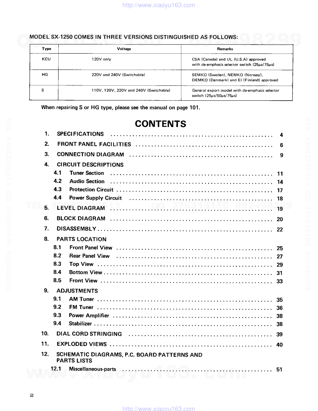
Type
Voltage
Remarks
KCU
120V only
CSA {Canada} and UL {U.S.A) approved
with de'emphasis selector switch (25psl75ps)
HG
22OV and 24OV (Switchable)
SEMKO {Sweden),
NEMKO (Norwav),
DEMKO (Denmark)
and El (Finland) approv€d
s
1IOV, 12OV,22OV and 240V {Switchable)
General export model with de-emphasis
selector
switch {25pslsops/75psl
MODEL SX.125O
COMES IN THREE VERSIONS
DISTINGUISHED
AS FOLLOWS:
When repairing S or HG type, please
see the manual on page 101.
CONTENTS
SPECIFICATIONS
FRONT PANEL FACILITIES
CONNECTION
DIAGRAM
CIFCUIT DESCRIPTIONS
4,1
Tuner Section
4.2
Audio Section
5.
6.
7.
8.
4 . 3 P r o t e c t i o n
C i r c u i t .
. . . . . . . , .
1 7
4.4 Power
Supply
Circuit
.......
18
L E V E L
D I A G R A M . , . .
. . . . . . . . . 1 9
B L O C K
D f A G R A M . . . . .
. . . . . . . 2 0
D l s A s s E M B L Y .
. . . . . . . . 2 2
PARTS LOCATION
8 . 1 F r o n t P a n e l
V i e w . .
. . . . . . . .
2 5
4 . 2 R e a r
P a n e l
V i e w
. . . . . . . . . , 2 7
8 . 3 T o p V i e w
. . . . . . . . 2 9
8 . 4 B o t t o m
V i e w
. . . . . ,
3 1
8 . 5 F r o n t
V i e w
. . . . . . . 3 3
ADJUSTMENTS
9.1 AM Tuner
. .. . 3b
9 . 2 F M T u n e r
. . . . . . . . . . . 3 6
9 . 3 P o w e r
A m p l i f i e r
. . . . . . . . . . . 3 8
9 . 4 S t a b i l i z e r
. . . . . . . . . . 3 8
D I A L C O R D S T R I N G I N G
. . . . . . . . 3 9
EXPLODED
VIEWS .
... . 40
SCHEMATIC
DIAGRAMS,
P.C. BOARD PATTERNS
AND
PARTS LISTS
1 .
2.
3.
4.
4
6
I
1 1
1 4
9.
I
i
I
10.
1 1 .
12.
51
12.1 Miscellaneous-parts
I
www. xiaoyu163. com
QQ 376315150
9
9
2
8
9
4
2
9
8
TEL 13942296513
9
9
2
8
9
4
2
9
8
0
5
1
5
1
3
6
7
3
Q
Q
TEL 13942296513 QQ 376315150 892498299
TEL 13942296513 QQ 376315150 892498299
http://www.xiaoyu163.com
\o
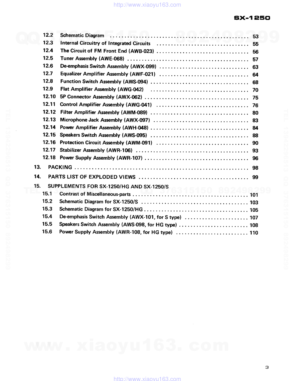
12.2
12.3
12.4
12.5
12.6
12.7
12.8
12.9
12.10
12.11
12.12
12.13
12.14
12.15
12.16
12.17
12.18
sx-1 25C,
Schematic Diagram
Internal Circuitry of Integrated Circuits
The Circuit of FM Front End (AWB-023)
Tuner Assembly (AWE-0681
De+mphasis Switch Assembty (AWX-099)
Equalizer Amplifier Assembly (AWF-021
)
Function Switch Assembly (AWS-094)
Flat Amplifier Assembly (AWG-042)
5P Connector Assembly (AWX-062)
Control Amplif ier Assembly (AWG-0411
Filter Amplif ier Assembly (AWM-089)
Microphone Jack Assembly (AWX-@71
Pourer Amplif ier Assembly (AWH-048)
Speakers Switch Assembly (AWS-G}S)
Protection Circuit Assembly (AWM-091)
Stabilizer Assembly (AWR-l 06)
Power Supply Assembly (AWR-I07)
PACKING
PARTS LIST OF EXPLODED
VIEWS .
SUPPLEMENTS
FOR SX-l250/HG AND SX-1250/5
15.1 Contrast
of Miscellaneous-parts
..
........101
15.2 Schematic
Diagram
for SX-1250/S
.....lO3
15.3 Schematic
Diagram
forSX-l2sOlHG.
..... lOb
15.4 De-emphasis
Switch Assembly
(AWX-101,
for S type) ..
.....1O7
15.5 Speakers
Switch Assembly
(AWS.098,
for HG type)
........
108
15.6 Poriver
Supply Assembly
(AWR-108,
for HG type)
.........110
s3
55
56
57
63
64
68
70
75
76
80
83
84
88
90
93
96
98
99
13.
14.
15.
I
a
!
www. xiaoyu163. com
QQ 376315150
9
9
2
8
9
4
2
9
8
TEL 13942296513
9
9
2
8
9
4
2
9
8
0
5
1
5
1
3
6
7
3
Q
Q
TEL 13942296513 QQ 376315150 892498299
TEL 13942296513 QQ 376315150 892498299
http://www.xiaoyu163.com
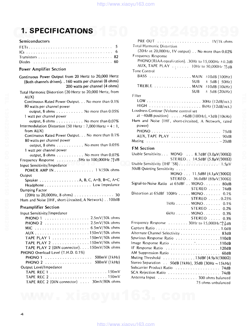
1. SPECIFICATIONS
Semiconductors
F E T S . . . .
. . . . . . 5
| C s . . . . .
. . . . . . 6
T r a n s i s t o r s
. . . . . . 8 2
D i o d e s
. .
. . . . . . 6 0
Power Amplif ier Section
C.ontinuous
Power Output from 20 Hertz to 20,000 Hertz
(Both channels
driven). . 160 watts per channel (8 ohms)
200 watts Per channel (4 ohms)
Total Harmonic Distortion (20 Hertz to 20,000 Hertz, from
AUX)
Continuous Rated Power Output. . . No more than 0.1%
80 watts per channel power
output, 8 ohms
. . . No more than 0.05%
1 watt per channel power
output,8 ohms
. . . No more than O.O7%
Intermodulation
Distortion
(50 Hertz : 7,000 Hertz = 4: l,
from AUX)
Continuous Rated Power Output. . . No more than 0 1%
80 watt! per channel power
output,8 ohms
. . . No more than 0.05%
1 watt per channel power
output, S ohms
. .
No more than 0.O1%
F r e q u e n c y
R e s p o n s e
. . . . . . . . . 5 H 2 t o 1 0 0 , 0 0 0 H 2 i l d B
Input Sensitivity/
| mpedan
ce
P O W E R
A r \ 4 P
| N . . . . . . . . .
Output
S p e a k e r . .
Headphone
Damping
Factor
. . . . . . . 1 V / 5 0 k o h m s
. A, B, C, A+8, B+C, A+C
. . . . . .
L o w l m p e d a n c e
( 2 0 H 2
t o 2 0 , 0 0 0 H 2 , 8
o h m s )
.
. . . . . . . 3 0
Hum and Noise (lHF, short-;ircuited,
A Network) . .100d8
Preamplif ier Section
Input Sensitivity/
lmped
ance
PHONO I
PHONO 2
t \ 4 t c . . . .
A U X , . . ,
T A P E P L A Y I . . . . . ,
T A P L P L A Y 2 . . . . . .
TAPE PLAY 2 (DlN conne(lor).
. .
PHONO
Overload
Level
(T.H.D.
0.1%)
PHONO I
PHONO
2
Output Level/l
mpedance
T A P L
R E C
I . . . , . ,
T A P E R L C 2 . . . . . .
TAPE REC 2 (DlN connector)
. . .
PRE OUT
Total lllrmonic Distortion
(20Hr ot 20,000Hr, I V ourpur) . . No more than O.02%
Frcquency
Rcsponse
PHONO
{R IAA equ,rlizrrion).
.30}12
ro 15,000H2
r0.2dB
A U X , T A P E
P L A Y . . . . . . .
t O H z t o 5 0 , 0 0 0 H . , l l d B
Tone Control
B A S S . . .
I ' R E B L E .
Filter
L O W . . . .
l V / 1 k o h m s
80dB
7 4dB
0.1%
H I G H , . .
Loudness
Contour (Volume control set
at 40dB position) . . . . .+6dB (100H2),
+3dB (t okHz)
Hum and Noise (lHF, short,circuited,
A Network, rated
power)
P H O N O . . . . . . . .
AUX, TAPE PLAY
l\4uting
..
FM Section
Usable
Sensitivity.
. . l\40No ..
S T E R E O . .
U s a b l e
S e n s i t i v i t y
( l H F ' 5 8 )
. . . . .
5 0 d B Q u i e t i n g
S e n s i t i v i t y
. . . .
l\40No . . .
S T E R E O . .
Signal-to-Noise
Ratio at65dBf . .
D i s t o r t i o n
a t 6 5 d B f l 0 0 H z . . . . .
l k H z . . . . . .
6 k H z .
. . [ 4 A l N 1 l 0 d B ( l 0 0 H z )
S U B t s d B ( s 0 H z )
. . l\4AlN 1'l0dB (tokHz)
S U B
t 5 d B ( 2 0 k H z )
. . 3 0 H z ( 1 2 d B / o c t . )
. . 8 kHz (12dB/oct.)
. . . 7 5 d B
. . . 9 0 d B
. . 20dB
8.7dBf (3.orv/300s})
l a.sdBf (s.8gV/300[l)
. . 1.5irV
11.sdBf
(a.1pV/3000)
36.0dBf
(69sV/300())
M O N O . . . . . . .
S T E R E O . . . . .
i \ 4 0 N o . . . . . .
S T E R E O . . . .
M O N O . . .
. . .
S T E R E O . . . .
. 0.25%
. 0 . 1 %
. 0.2/o
. 2.5mV/50k ohms
. 2.5mV/50k ohms
. 6.5mV/50k ohms
. 1 50mV/50k ohms
. 1 50mV/50k ohms
. I 50mv/50k ohms
. 150mV/50k ohms
. . 500mV (1 kHz)
. . s00mV (1kHz)
. . . . . . . . 1 5 0 m V
. . . . . . . . 1 5 0 m V
. 30mV/80k ohms
Frequency
Response
. . . l \ 4 0 N o
. . . . . . . 0 . 3 %
STEREO . . . . . O.3Vo
. . 30Hz to l5,000Hri?
3dB
C a p t u r e
R a t i o
. . . . . . . . . . l . O d B
A l t e r n a t c C h a n n e l S e l e c t i v i t y
. . . . . . . .
8 3 d B
S p u r i o u s
R e s p o n s e
R a t i o . . .
. . . . . . . 1 1 O d B
l m a g e
R c s p o n s e
R a t i o
. . .
. . . . . . . . . 1 1 0 d 8
l F R e s p o n s e
R a t i o . . .
. . . 1 2 0 d 8
A M S u p p r e s s i o n
R a t i o
. . .
. . . . . . . . . 6 0 d 8
/ V l u t i n g T h r e s h o l d
. . . . . 1 3 d B f ( 4 . 9 p v l 3 0 0 4 )
Stereo Separation . . 50dB (lkHz), 35dB (30H2-t5kHz)
S u b c a r r i e r P r o d u c t R a t i o
. . . . . . . . . .
1 4 d B
S C A R e j e c t i o n
R a t i o
. . .
. . . . . . . . . . 7 4 d 8
Antenna Input
300 ohms balanced
75 ohms unbalanced
I
I
www. xiaoyu163. com
QQ 376315150
9
9
2
8
9
4
2
9
8
TEL 13942296513
9
9
2
8
9
4
2
9
8
0
5
1
5
1
3
6
7
3
Q
Q
TEL 13942296513 QQ 376315150 892498299
TEL 13942296513 QQ 376315150 892498299
http://www.xiaoyu163.com
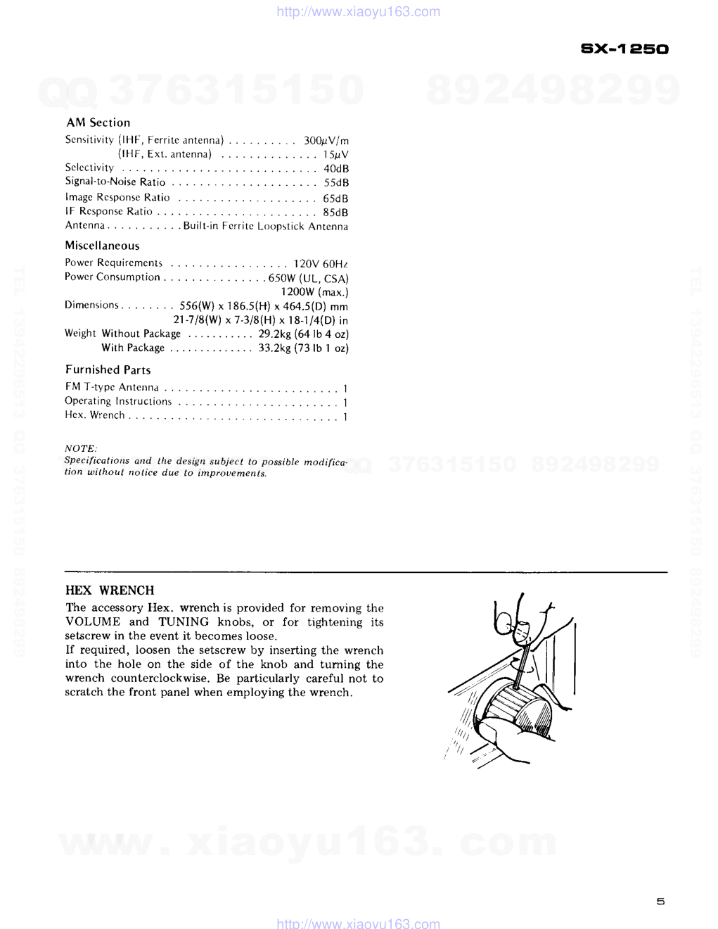
six-1 Elscl
A\,?
AM Section
Scnsitivity
(lHF, Ferritc antenna)
(lll F, Ext. antenna)
Sclcctivity
S i g n a l - t o - N o i s e
R a t i o . . . . . . . .
l m a g e
R c s p o n s e
R a t i o . . . . . . .
lF Rcsponse
Ratio . . .
Antenna
. .
l\4iscellaneous
Power
Rcquircmcnts
. . . 1 2 0 V
6 0 H Z
. . . . . . . 6 s 0 w ( u L , c s A )
'1200W
(max.)
Powcr Consumption
D i m e n s i o n s . . . . . . . .
5 5 6 ( W )
x 1 8 6 . 5 ( H )
x 4 6 4 . 5 ( D )
m m
21-7l8(w)
x 7.3/8(H)
x 181/4(D) in
Weight Without Packag€
.
. 29.2kg(641b
4 oz)
With Package
..... 33.2kg
(73 lb 1 oz)
. Built'in Fcrrite
. . . . . . 3 0 0 p V / m
. . . . . . . . . l 5 i r v
. . . . . . . . . 4 0 d 8
. . . . . . . . . 5 5 d 8
. . . . . . . . . 6 5 d B
. . . . . . . . . 8 5 d B
Loopstick
Antenna
Furn ished Parts
Fl\4 T-typc Antcnnd . .
Opcrating
Instructions
Hex. Wrench
. 1
, 1
. t
NOTE:
Specifications
ond the desigtr subject to possible modifica.
tion uithout notice due to improuements.
s
HEX WRENCH
The accessory Hex. wrench is provided for removing the
VOLUME and TUNING knobs, or for tightening its
setscrew in the event it becomes loose.
If required, loosen the setscrew by inserting the wrench
into the hole on the side of the knob and tuming the
wrench counterclockwise. Be particularly careful not to
scratch the front panel when employing the wrench.
5
www. xiaoyu163. com
QQ 376315150
9
9
2
8
9
4
2
9
8
TEL 13942296513
9
9
2
8
9
4
2
9
8
0
5
1
5
1
3
6
7
3
Q
Q
TEL 13942296513 QQ 376315150 892498299
TEL 13942296513 QQ 376315150 892498299
http://www.xiaoyu163.com
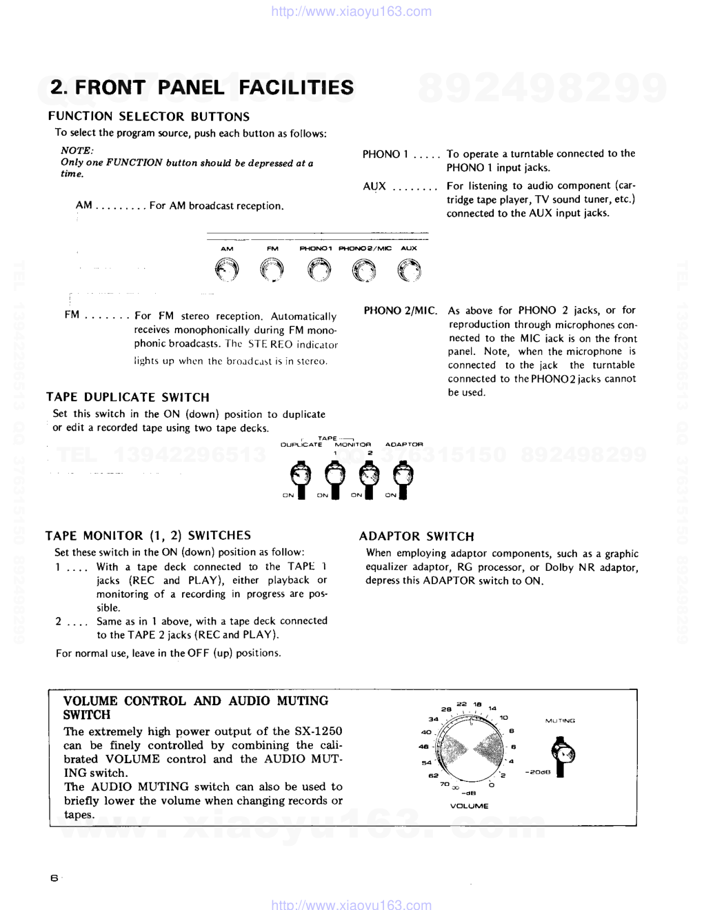
2. FRONT PANEL FACILITIES
FUNCTION SELECTOR BUTTONS
To select the program source, push each button as follows:
NOTE:
Only one FUNCTION button should be depresaed ot o
ttme.
A M . . . . . . . . .
F o r A M b r o a d c a s t r e c e p t i o n .
P H O N O
1 . . . . .
A U X . . . . . . . .
o o o
A
\ - ' o
. . . . For FlVl stereo reception. Automatically
receives
monophonically during FlVl mono-
phonic broadcasts.
Th0 5TE REO indic.rror
l i i h t s u p w h e n l h e b r " J , l L . r . t
r \ n \ l c r c u .
PHONO 2/MtC.
TAPE DUPLICATE SWITCH
Set thi5 switch in the ON (down) position to duplicate
or edit a recorded tape using two tape decks.
To operate a turntable connected to the
PHONO 1 input jacks.
For listening to audio component (car-
tridge tape player, TV sound tuner, etc.)
connected to the AUX input jacks.
As above for PHONO 2 iacks, or for
reproduction through microphones
con-
nected to the Mlc iack is on the front
panel. Note, when the microphone is
connected to the iack the turntable
connected to the PHONO2 iacks cannot
De useo.
FM
VOLIJME CONTROL AND AUDIO MUTING
SWITCH
The extremely high power output of the SX-1250
can be finely controlled by combining the cali-
brated VOLUME control and the AUDIO MUT-
ING switch.
The AUDIO MUTING switch can also be used to
briefly lower the volume when changing records or
taDes.
r
VOL!ME
.-.
I
rt
I
IItII
i
i
I
vItI
'I
I
It
I
IIIIii
YII
ADAPTOR SWITCH
When employing adaptor components, such as a graphic
equalizer adaptor, RG processor, or Dolby NR adaptor,
depress this ADAPTOR switch to ON.
s ? F $
TAPE MONTTOR (1, 2) SWTTCHES
Set these switch in the ON (down) position as follow:
1 .. .. With a taDe deck connected to the TAPE I
jacks (REC and PLAY), either playback or
monitoring of a recording in progre5s are pos-
sible.
2 .. .. Same as in 1 above, with a tape deck connected
to the TAPE 2 jacks (REC and PLAY).
For normal use, leave in the OFF (up) positions.
www. xiaoyu163. com
QQ 376315150
9
9
2
8
9
4
2
9
8
TEL 13942296513
9
9
2
8
9
4
2
9
8
0
5
1
5
1
3
6
7
3
Q
Q
TEL 13942296513 QQ 376315150 892498299
TEL 13942296513 QQ 376315150 892498299
http://www.xiaoyu163.com
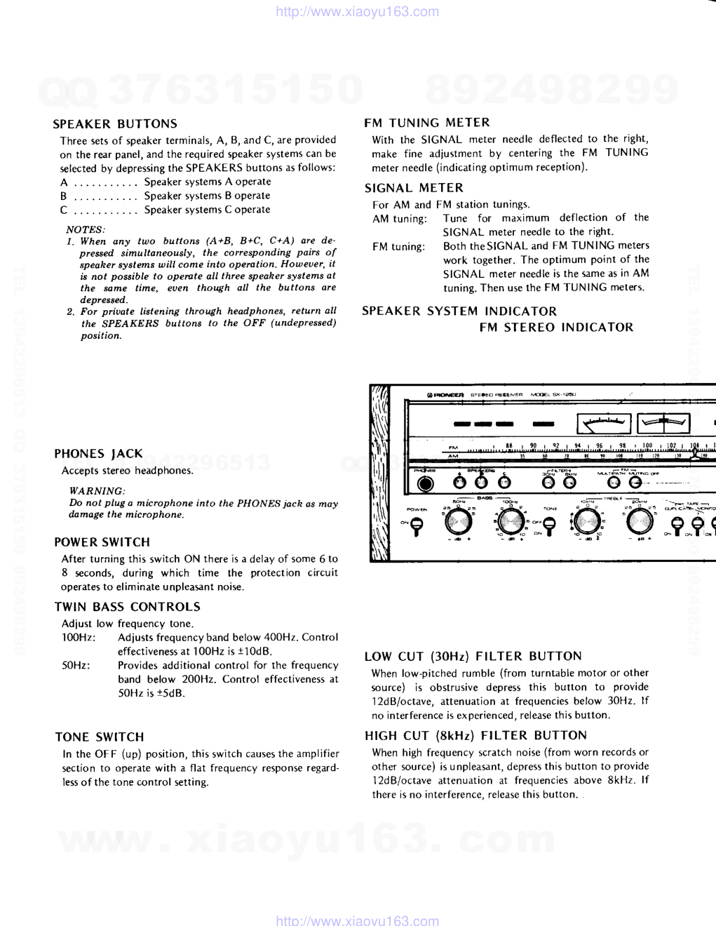
SPEAKER
BUTTONS
Three sets of speaker terminals, A, B, and C, are provided
on the rear panel, and the required speaker systems can be
selected by depressing
the SPEAKERS buttons as follows:
A . . . . . . . . . . .
S p e a k e r
s y s t e m s A o p e r a t e
B . . . . . . . . . . .
S p e a k e r
s y s t e m s
B o p e r a t e
C , . . . . . . . . . .
S p e a k e r
s y s t e m s
C o p e r a t e
NO?ESr
1. Whetr any two buttons (A+8, B+C, C+A) ore de'
preaeed simultaneously, the eorresponding pairs of
speaker systems will come into operation. Howeuer, it
is not possible to operote all three speaher systems ot
the same time, euen though all the buttons ore
depressed.
2. For priuote listening through heodphones, return all
the SPEAKERS buttons to the OFF (undepressed)
Dosition.
PHONES 'ACK
Accepts stereo headphones.
WARNING:
Do not plug a microphone into the PHONES jach os may
domage the microphone.
POWER
SWITCH
After turning this switch ON there is a delay of some 6 to
8 seconds, during which time the protection circuit
operates to eliminate unpleasant norse.
TWIN BASS CONTROLS
Adiust low frequency tone.
100H2:
Adiusts frequency band below 400H2. Control
effectiveness
at 100H2 is r10dB.
50Hz:
Provides additional control for the frequency
band below 200H2. Control effectiveness
at
50Hz is r5dB.
TONE SWITCH
In the OFF (up) position, this switch causes
the amplifier
section to operate with a flat frequency response regard'
less of the tone control setting.
FM TUNING METER
With the SIGNAL meter needle deflected to
make fine adiustment by centering the FM
meter needle (indicating
optimum reception).
SIGNAL METER
the right,
TUN ING
TU
Sel
ob
st
Ft\
Le
For AN4 and
Al\4 tuning:
FM tuning:
Flvl station tunings.
Tune for maximum deflection of the
SIGNAL meter needle to the right.
Both the SIGNAL and FM TUN ING meters
work together. The optimum point of the
SIGNAL meter needle
is the same as in AM
tuning. Then use the Fl\4 TUNING rn€ters.
su
tw
su
oe
SPEAKER
SYSTEM INDICATOR
FM STEREO INDICATOR
LOW CUT (30H2) FILTER BUTTON
when low-oitched rumble {from turntable motor or other
source) is obstrusive depress this button to provide
l2dBloctave, attenuation at frequencies below 30H2. lf
no interference is experienced,
release
this button.
HIGH CUT (8kHz) FILTER BUTTON
When high frequency scratch noise (from worn records or
other source) is unpleasant,
depress this button to provide
12dB/octave attenuation at frequencies above 8kHz. lf
there is no interference,
release
this button.
FM
W
oe
the
tnt
A
10
T
20
www. xiaoyu163. com
QQ 376315150
9
9
2
8
9
4
2
9
8
TEL 13942296513
9
9
2
8
9
4
2
9
8
0
5
1
5
1
3
6
7
3
Q
Q
TEL 13942296513 QQ 376315150 892498299
TEL 13942296513 QQ 376315150 892498299
http://www.xiaoyu163.com
I of the
t.
G meters
nt of the
as in AM
m€Iers.
TOR
or other
provide
lOHz. lf
rcords
or
,provide
3kHz. lf
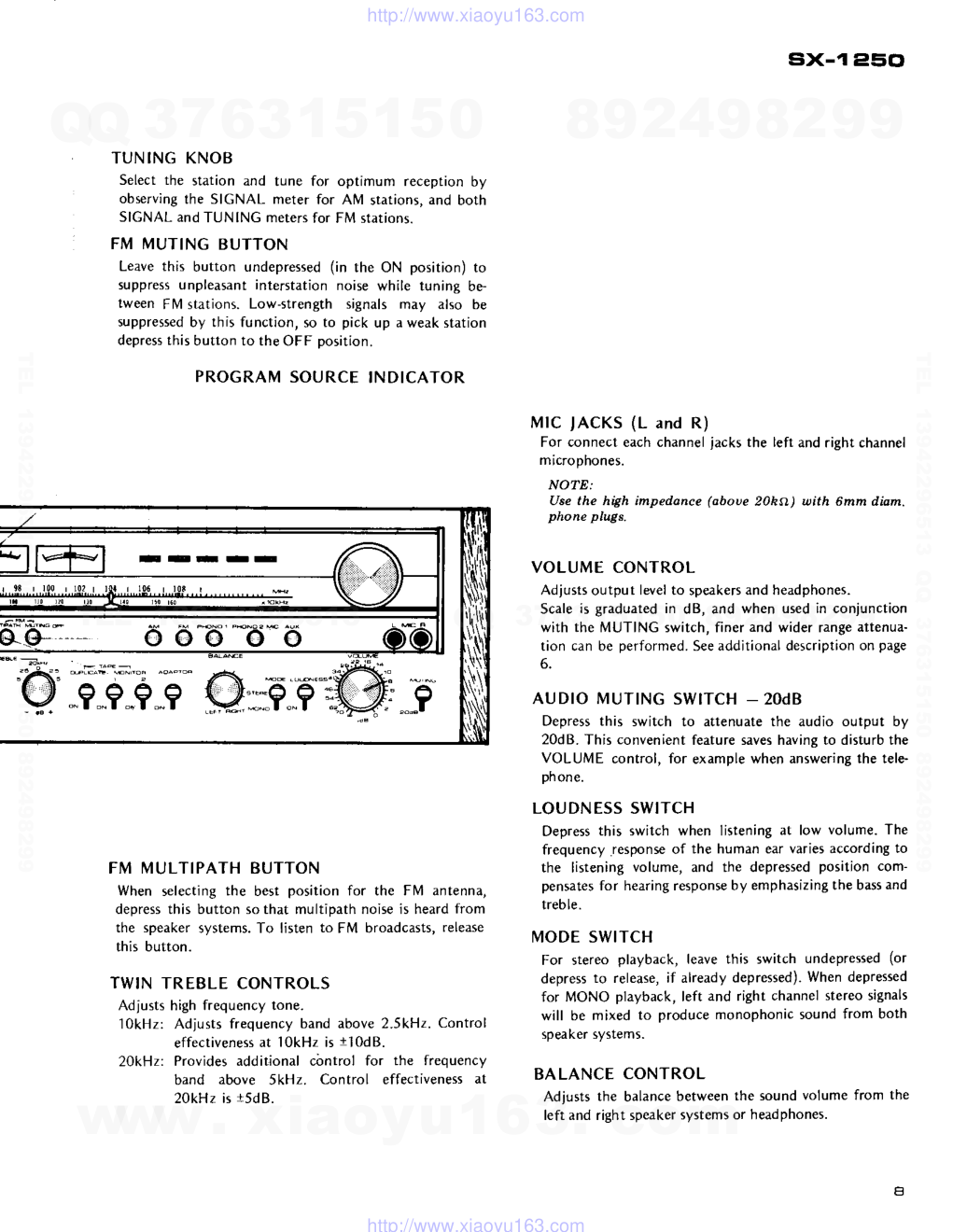
TUNING KNOB
Select the station and tune for optimum reception by
observing the SIGNAL meter for AlVl stations, and both
SICNAL and TUNING meters for FM stations.
FM MUTING BUTTON
Leave this button undepressed (in the ON position) to
suppress unpleasant interstation noise while tuning be-
tween F l\4 stations. Low-strength signals may also be
suppressed
by this function, so to pick up a weak station
depress
this button to the OFF position.
PROGRAM SOURCE INDICATOR
FM MULTIPATH BUTTON
When selecting the best position for the Fl\4 antenna,
depress this button sothat multipath noise is heard from
the speaker systems. To listen to FN,l broadcasts,
release
this button.
TWIN TREELE CONTROLS
Adjusts high frequency tone.
1okHz: Adjusts frequency band above 2.5kHz. Control
effectiveness
at lokHz is r10dB.
20kHz: Provides additional control for the frequency
band above 5kHz. Control effectiveness at
20kHz is r5d B.
six-1 e50
MIC JACKS (L and R)
For connect each channel jack5 the left and right channel
microphone5.
NOTE:
Use the hEh impedance (oboue 20ks7) with 6mm diatn.
phone plugs.
VOLUME CONTROL
Adjusts output level to speakers
and headphones.
Scale is graduated in dB, and when used in conjunction
with the MUTING switch, finer and wider range attenua-
tion can be performed. See additional description on page
6.
AUDIO MUTING SWITCH _2OdB
Depress this switch to attenuate the audio output by
20dB. This convenient feature saves having to disturb the
VOLUME control, for example when answering the tele-
ph on e.
LOU DN ESS SWITCH
Depress this switch when listening at low volume. The
frequency response of the human ear varies according to
the listening volume, and the depressed position com-
pensates
for hearing response
by emphasizing
the bass and
treble.
IIIODE SWITCH
For stereo playback, leave this switch undepressed
(or
depress to release, if already depressed).
When depressed
for MONO playback, left and right channel stereo signals
will be mixed to produce monophonic sound from both
speaker systems.
BALANCE CONTROL
Adjusts the balance between the sound volume from the
left and right speaker systems or headphones.
right,
o 6ru'"-6*6
www. xiaoyu163. com
QQ 376315150
9
9
2
8
9
4
2
9
8
TEL 13942296513
9
9
2
8
9
4
2
9
8
0
5
1
5
1
3
6
7
3
Q
Q
TEL 13942296513 QQ 376315150 892498299
TEL 13942296513 QQ 376315150 892498299
http://www.xiaoyu163.com
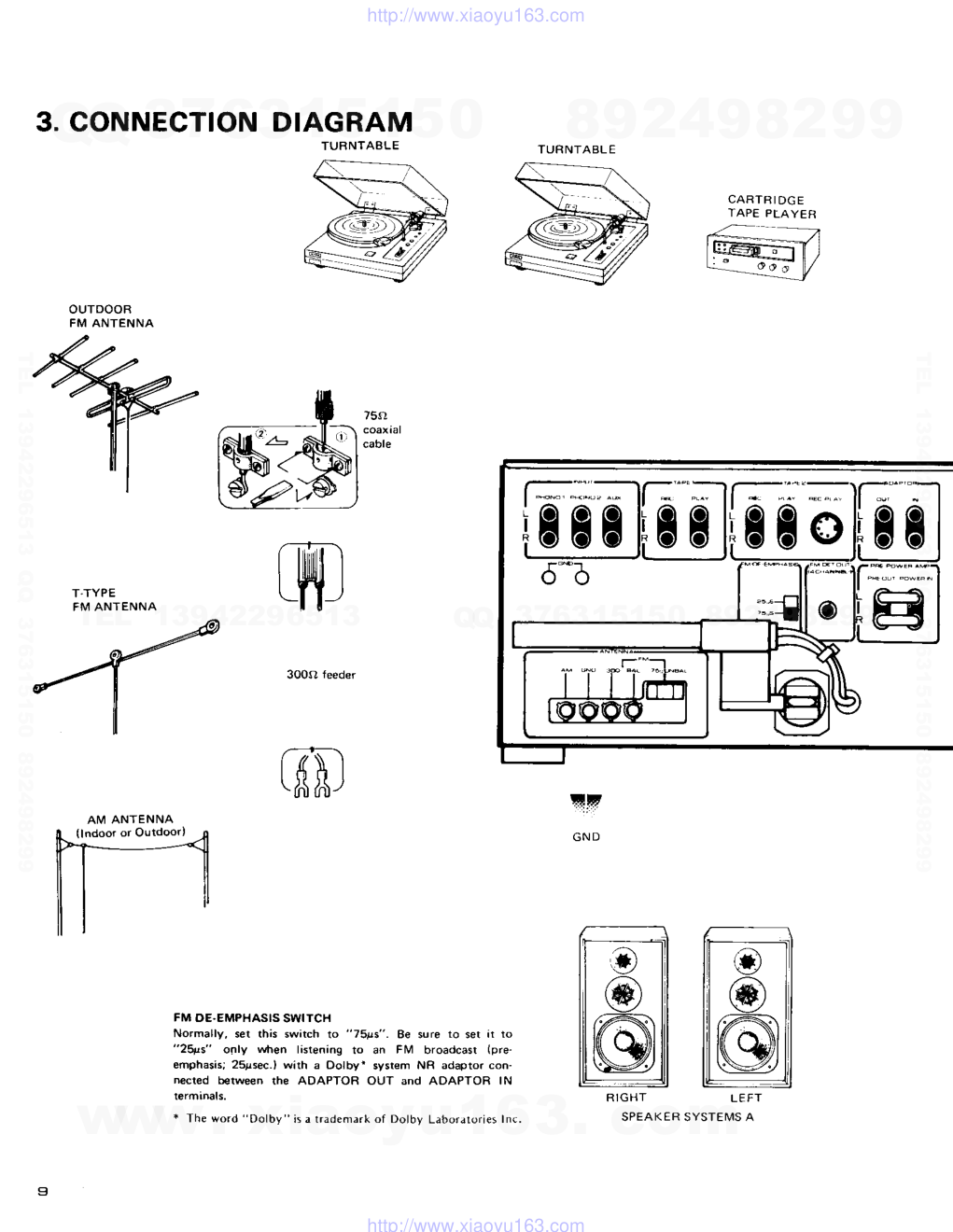
3. CONNECTION DIAGRAM
TURNTAELE
OUTDOOR
FM ANTENNA
T.TYPE
FM ANTENNA
TAPE
3O0A teeder
FM OE.EMPHASIS SWITCH
Normally, set this swatch to "75!s".
Be sure to set ir to
"25ps"
only
when listening to an F[,
broadcast (pre-
ernphasis; 25rrsec.l with a Oolby'
system NR adaptor con-
nected berween the ADAPTOR
OUT and ADAPTOR
lN
* The word "Dolby" i! a trademark of Dolby Laboratories Inlj.
ffi-[]
4.V
G N D
TURNTABL
E
R I G H T
LEFT
R I G
S P E A K E R S Y S T E M S A
www. xiaoyu163. com
QQ 376315150
9
9
2
8
9
4
2
9
8
TEL 13942296513
9
9
2
8
9
4
2
9
8
0
5
1
5
1
3
6
7
3
Q
Q
TEL 13942296513 QQ 376315150 892498299
TEL 13942296513 QQ 376315150 892498299
http://www.xiaoyu163.com
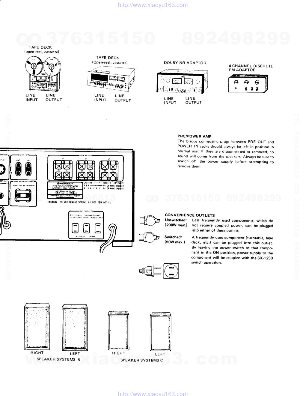
IAPE OECK
(open{eel, casselre}
L I N E
L I N E
INPUT
OUIPUT
L I N E
L I N E
INPU-T
OUTPUT
irulr(il -00 r0r ftrovt ScRtyis
yr 30r rtr 0T ct
D O L B Y N R A D A P T O R
4 C H A N N E L D I S C R E T E
FM ADAPTOR
o s e
. I e 0
L I N E
L I N E
INPUT
OUTPUT
PR€/POWE R AMP
The bridg€ connecting plugs beiween pRE OUT and
POWER lN iacks should always be teft in position in
normal us€. ll rhey are disconnected or removed, no
sound will come from the speakers. Atways be sure to
swatch off the power supply before artempring to
CONVENIENCE
OUTLETS
Unswitchod: Less frequentty used components, which do
l2O0W max.) not require coupled power, can be ptugged
into either ot these outlets.
A frequ€ntly used component (turntabte, tape
deck. elc.) can be plugged into this outlet.
By leaving the power switch of rhat compo,
nent in the ON position, povver suppty ro the
componenr wi
be coupled with the sx_1250
switch operation.
l r
t P
t - t t - t t - l
t=J t=J u
Switchsd:
(sow max.l
Itl:i.i+l
rl '
EE
R I G H T
L E F T
R I G H T
S P E A K E R S Y S T E M S 8
S P E A K E R S Y S T E M S C
www. xiaoyu163. com
QQ 376315150
9
9
2
8
9
4
2
9
8
TEL 13942296513
9
9
2
8
9
4
2
9
8
0
5
1
5
1
3
6
7
3
Q
Q
TEL 13942296513 QQ 376315150 892498299
TEL 13942296513 QQ 376315150 892498299
http://www.xiaoyu163.com
\ f
4. CIRCUIT DESCRIPTIONS
4.1 TUNER SECTION
FM Front End
The FM front end is composed of a tuning circuit
employing a 5-gang variable capacitor, a 2-stage RF
amplifier and mixer employing dual gate MOS
FETs, and a local oscillator with buffer. An equiva-
lent of a cascode amplifier is produced by AC
grounding gate-2 of the dual gate MOS FET,
allowing stable RF amplification at high gain.
The output signal of the RF amplifier is applied to
gate-1 of the mixer stage MOS FET, while the loca.l
oscillator output signal is applied to gate-2. This
technique minimizes input power ftom the local
oscillator, resulting in low mutual interference even
if the received signal input level is high.
A variation of a Clapp circuit forms the local
oscillator. Inclusion of a buffer amplifier between
local oscillator and mixer reduces local oscillator
load, eliminating distortion of the oscillation wave-
form. Drawing effect of the local oscillator is also
eliminated.
15 !rut8at.
Etx-1 ElEiCt
FM lF Section
Four integrated circuits (ICs) and four dual element
ceramic filters compose this section. HA1201
(diagram on page 56) is a differential amplifier with
a constant current source and functions as a
current-limiting limiter. HA1137 (diagram on page
55) contains IF limiter amplifier, quadrature detec-
tor, meter drive and muting circuits. The detector
circuit contained within this IC is not used in the
SX-1250 however, and instead the IF signal is
taken ftom the stage prior to the detector and
applied to TA7061AP. This latter IC is a 3-stage
differential amplifier (diagam on page 56) and its
output goes to the ratio detector for FM detection.
t-
100 0 0 ..
L
Fig. L Circuitry of Flvl tront end
Fig. 2. Block diagram
for HA1137
www. xiaoyu163. com
QQ 376315150
9
9
2
8
9
4
2
9
8
TEL 13942296513
9
9
2
8
9
4
2
9
8
0
5
1
5
1
3
6
7
3
Q
Q
TEL 13942296513 QQ 376315150 892498299
TEL 13942296513 QQ 376315150 892498299
http://www.xiaoyu163.com
Multiplex Decoder
The multiplex decoder contains three sections and
employs an IC (HA1196) with a block diagram as
shown in Fig. 3 (see page 55 for circuit).
1. Switching Signal Generator
A PLL (phase locked loop) system is employed.
76kHz is generated by the VCO (voltage controlled
oscillator: an oscillator in which frequency is
controlled by a voltage) and converted into 38kHz
by a frequency divider, then divided again to
become 19kHz. This signal and the stereo pilot
component (19kHz) of the detected signal are
applied to a phase comparator where the difference
between them is converted into a voltage. By
feedback this voltage is applied to the VCO. And
the oscillator sig4al is locked to the pilot signal.
This loop is termed PLL and a 38kHz switching
signal synchronized to the pilot signal is obtained
and employed as a switching signal.
2. Automatic stereo detector
With the PLL locked to the pilot sig.nal, the pilot
signal and a 19kHz signal of the same phase are
produced. A voltage is then obtained at the phase
comparator that is proportional to the pilot signal
amplitude. As it increases, the lamp lights and the
switch becomes on. The switching signal is applied
to the demodulator.
Conposilo
irgral
oulpur
F i g . 3 .
However, if the FM muting signal is also applied to
pin 12, the detector circuit becomes disabled
(grounded). Therefore a switching signal to the
demodulator is not supplied and mono reproduc-
tion is obtained.
3. Demodulator
Two differential amplifiers are employed in a
switching circuit (Fig. 4). The composite signal is
applied to the base of Q3. Q1 and Q2 are alter-
nately switched ON and OFF by the switching
signal. The composite signal amplified at Q3 is
demodulated by the switching of Q1 and Q2. Q6
and Q3 are loosely coupled at their emitters by R1,
R2 and R3. Q6 is driven in opposite phase to Q3
and its low level composite signal output is de-
modulated by switching of Q4 and Q5. The de-
modulated signals in opposite phase are combined
at the collectors of Q1 and Q2, cancelling crosstalk.
Adequate current flow is required in Q3 and Q6
for low distorbion. However, if the base bias voltage
is raised, the voltage range available at the collector
is reduced and clipping occurs (power supply
voltage is limited by IC voltage requirement). For
this reason, current from an external source is
inserted at Q3 and Q6 collectors and become 11
and I2 in Fig. 4. The same amount of curlent is
removed at the emitters of Q3 and Q6 to become
I3 and 14 in Fig. 4. Q3 and Q6 therefore operate
with adequate current and distortion in this stage is
remarkably reduced. A feedback amplifier amplifies
the demodulated signal to produce the IC outputs.
I'lrt ing
sip,l
Block diagram
lor HAl 196
I
I
I
www. xiaoyu163. com
QQ 376315150
9
9
2
8
9
4
2
9
8
TEL 13942296513
9
9
2
8
9
4
2
9
8
0
5
1
5
1
3
6
7
3
Q
Q
TEL 13942296513 QQ 376315150 892498299
TEL 13942296513 QQ 376315150 892498299
http://www.xiaoyu163.com
Ai0
FM Muting Circuit (Fig. 5)
DC voltage emetges from pin 12 of IC (HA1137) in
the event of more than l7OkHz detuning or low
input level (less than 4.9pV antenna input conver-
sion). This is employed for shorting the AF output
circuit to perform muting by the reed relay.
8X-1 25cl
Multipath Monitor Circuit
When multipath reflections exist in the received
signal, the signal is converted into AM and PM
(amplitude modulation
and phase modulation)
forms. Since the amplitude of the actual FM signal
is fixed, by converting this AM component into a
sound and listening to it, the existence (and
amount) of multipath reflection can be determined.
Short term level variations (audio frequency) are
taken as a signal from HA1137 SIGNAL meter
drive terminal
(pin 13). By setting the FM
MULTIPATH switch to ON during FM reception,
this signal becomes connected to the audio ampli-
fier and can be heard as a sound which indicates
conditions of multipath refl ection.
AM Tuner
The AM tuner employs a S-gang variable capacitor
and an IC (HA1138) with 1-stage of RF and 2-stage
of IF amplification. Fig. 6 shows the HA1138
block diagram (see page 55 for circuit).
Fig. 5. Circuitry of Fl\4 muting
It outprt
ciruuil
t
l
, " /
c {
* ) ,
lod
tatal
Fig. 4. Basic circuitry of demodulator
Schmitd
Dircuit
Fig. 6. Block diagram
for HA1 l38
www. xiaoyu163. com
QQ 376315150
9
9
2
8
9
4
2
9
8
TEL 13942296513
9
9
2
8
9
4
2
9
8
0
5
1
5
1
3
6
7
3
Q
Q
TEL 13942296513 QQ 376315150 892498299
TEL 13942296513 QQ 376315150 892498299
http://www.xiaoyu163.com
4.2 AUDIO SECTION
Equalizer Amplifier
The equalizer amplifier is shown in Fig. 7. The ftst
stage (Ql & Q2) is a PNP transistor unbalanced
differential amplifier. High voltage gain is provided
in the following stage (Q3) by a bootstrap circuit
(C1 & R1). The output stage (Q4 & Qb) is a com-
plementary symmetrical SEPP circuit. The high
voltage utility factor of the SEPP circuit provides a
high maximum output voltage. Dynamic range of
the equalizer amplifrer is therefore wide and over-
load input lettel at O.lVo distortion is 500mV (rms
at lkHz).
Equalizer elements (C2, C3, R2, R3) are polysty-
rene film capacitors with tolerances within 117o
and metal film resistors with tolerances better than
i1%. These lead to a deviation with respect to the
RIAA playback standard within t0.2dB. Due to
the balanced plus and minus power supply, the
input and the output points become essentially 0V,
reducing click noise during FUNCTION switch
operation.
Tape and Adaptor Circuits
With the DUPLICATE switch OFF, the program
source selected by the function switches are ob-
tained at the TAPE REC jacks (Fig. 8).
The TAPE MONITOR 1 switch selects between the
program source selectd by the function switch
and the input at the TAPE 1 PLAY jacks (Fig.9).
The TAPE MONITOR 2 switch selects between the
signal selected by the TAPE MONIIOR
1 switch
and the input at the TAPE 2 PLAY jacks (Fig.9).
IIPI I
ntt 2
Ptat
tut
9
9
I
Y
oxJ. -
oll-'"-
t":l':ffirno*'
lrtrrotrToRz
stllcll
rxitch
ixilch
Fig.9. TaPe monitor circuit
When the DUPLICATE
switch is set to ON, the
TAPE 1 REC jacks are connected to the TAPE 2
PLAY
jacks, and the TAPE 2 REC jacks to the
TAPE 1 PLAY jack's (Fig. 10).
Tltt I
IlPt 2
Fig. 10. Tape duplicate circuit
The signal selected by the TAPE MONITOR 2
switch appears at the ADAPTOR OUT jacks (Fig'
11). The ADAPTOR switch selects between the
signal selected by the TAPE MONITOR 2 switch
and the input at the A-DAPTOR IN jacks (Fig. 11)'
lll
TAPI I
ntc
TIPI 2
IrI
tt t0 l0t 2
rritch
r0ltl||t
sritch
Fig. 1 1. ADAPTOR iacks
tnctior
sritch
MODE Switch
When the MODE switch is set to the MONO posi
tion, the left and right channels are shorted in the
stage following the tape and adaptor circuits.
,l
l
t
i
i
R ,
c" [" t'
Fig. 7. Schematic diagram for Equalizer amplifier
1 4
Fig. 8. TAPE REC jacks
www. xiaoyu163. com
QQ 376315150
9
9
2
8
9
4
2
9
8
TEL 13942296513
9
9
2
8
9
4
2
9
8
0
5
1
5
1
3
6
7
3
Q
Q
TEL 13942296513 QQ 376315150 892498299
TEL 13942296513 QQ 376315150 892498299
http://www.xiaoyu163.com
-
A':o
BALANCE Control
A no-loss HB type variable resistor at center posi-
tion is employed. An SEPP circuit is inserted as a
buffer in the following stage.
Muting Circuit
When the MUTING switch is set to the -20dB
position, the signal is attenuated by 20dB.
Loudness Circuit
This circuit is operated ON or OFF by the LOUD-
NESS switch and is intended to compensate for
audibility characteristics of the human ear at low
volumes. The VOLUME control variable resistor is
tapped. Connecting a CR network at this point
enhances low and high frequencies at low volumes.
Tone Controls
Twin tone controls are employed with the SX-
1250. These consist of ultra-low and ultra-high
(sub) controls in addition to the conventional
BASS and TREBLE (main) controls.
The signal is amplified to required level by a 2-stage
FET and transistor direct coupled amplifier, after
which a 2-stage NFB type tone control ctcuit is
provided. The sub controls form the first stage and
the main controls form the second stage of this
circuit. With NFB type tone controls, C-B feedback
is applied to a single transistor amplifier. Frequency
response becomes variable by providing selectivity
in the feedback circuit. The basic circuit of this
stage is shown in Fig. 12.
BX-1 25Ct
Fig. 13. Midrange
operation
of NFB type
tone control circuit
Low Frequency Operation
The reactance of C1 and C2 increases at low fte-
quency to form a circuit as shown in Fig. 14. This
reactance increases in proportion to the frequenry
declines. Also, the NFB amount varies greatly
according to VR1 slider position. The circuit gain
at low frequencies can therefore be varied by VR1.
Fig. 14. Low frequency operation of NFB type
tone control circuit
High Frequency Operation
The considerably smaller reactance of C1 and C2 at
high frequency in comparison with VRl effectively
shorts VR1 to from an equivalent circuit such as
that shown in Fig. 15. C3 reactance decreases in,
the same degree that the frequency increases and
the NFB amount is now mainly controlled by the
VR2 slider position. Consequently, the gain at
high frequencies can be varied by VR2.
High frequency operation of N
tone control circuit
hpn
I ,
vn,
t ?
[,-c, { Pc "
n .
I c "
)
0rt!!t
t.
tt,
[.
Fig. 12. Basic
circuitry of NFB type tone control circuit
Midrange Operation
The Cl and C2 reactances are considerably smaller
thal VRl
at frequencies above midrange, effec-
tively shorting VRl. At frequencies below mid-
range, C3 reactance becomes large and in effect,
opens the circuit. Consequently, the circuit be-
comes equivalent to that shown in Fig. 13 with
respect to the midrange. In this figure, the circuits
parameters are not changed by any change in posi-
tion of the VR1 and VR2 sliders. Ttre NFB amount
is therefore fixed and the circuit gain is also fixed
without regard to VR1 and VR2 slider positions.
Fis. 15.
FB type
www. xiaoyu163. com
QQ 376315150
9
9
2
8
9
4
2
9
8
TEL 13942296513
9
9
2
8
9
4
2
9
8
0
5
1
5
1
3
6
7
3
Q
Q
TEL 13942296513 QQ 376315150 892498299
TEL 13942296513 QQ 376315150 892498299
http://www.xiaoyu163.com
Tone Defeat Circuit
By setting the TONE switch to OFF, the above
described tone control circuit becomes bypassed.
Filter Circuits ( Fig. 16)
These are NFB type active filters with -12dB/
octave slopes. The circuit combines a 2-stage CR
element and emitter follower. Normal function of
the emitter follower is provided in the passband
and by 100% NFB, gain becomes essentially "1".
NFB is cancelled in the area of the cutoff fre-
quency, composing a peak in the frequency re-
sponse. This leads to improved and sharper CR
filter response. In the actual circuit, CR elements
for low and high filters both employ the same
emitter follower and each can be selected ON-OFF.
Power Amplifier
Fig. 17 shows the power amplifier section. The
input stage is composed of Q1 & Q2 differential
amplifier, with the input signal applied to e1. eg
& Q4 differential amplifier comprise the second
stage, with Q3 output composd at Q4 by Qb &
Q6 cunent mirror. Connecting collector and base
of Q5 produces the equivalent of a diode. Q3
collector cunent produces a forward voltage be-
tween Qb base and emitter, biasing Q6. Rl and R2
in this circuit are equal, while Qb arrd Q6 are the
same type transistors. Consequently, when voltages
between bases and emitters of Qb & Q6 are equal,
cunent flows in these transistors also become
equal. This results in equal current flows in Q3 and
Q6. Mutually opposite phase signals drive Q3 and
Q4, resulting in mutually opposite phase collector
cunents. Q4 and Q6 therefore operate as push-pull.
+fcc.
Fig. 16. Basic
circuitry of filters
Power stage bias voltage is supplied by the voltage
drop across D1, D2 and VR2. VR2 is a semi-fixed
resistor for power stage bias adjustment, while D1
and D2 are Varistors for temperature compen-
sation.
A 3-stage Darlington connection is employed in the
power stage (Q7-Q14),
with output transistors
Q11-Q14 in a complementary symmetrical parallel
+ YcC,
Il0[ tlLTIn sritch
:
r
i
I
tl
s
Fig. 17. Schematic diagram for power amplifier
www. xiaoyu163. com
QQ 376315150
9
9
2
8
9
4
2
9
8
TEL 13942296513
9
9
2
8
9
4
2
9
8
0
5
1
5
1
3
6
7
3
Q
Q
TEL 13942296513 QQ 376315150 892498299
TEL 13942296513 QQ 376315150 892498299
http://www.xiaoyu163.com
AO
connection. The output center point is at 0V from
the balanced plus and minus power supply, while
LOOT> DC NFB is applied to Q2 through R3.
Because of this, circuit DC gain becomes OdB and
DC voltage of the output center point is deter-
mined by Ql base voltage. VR1 is a semi-fixed
resistor for fine adjustment of the center point
voltage to compensate for irregularities in circuit
elements.
SPEAKERS Switches
The SX-1250 is provided with 3 sets of speaker
terminals (A, B, C). Since the power amplifier can
become overloaded if all three sets are used simul-
taneously, when all 3 SPEAKERS switches are set
to ON, the circuit functions as if all switches were
OFF and the indicator lamps extinguish.
4.3 PROTECTION CIRCUIT
This circuit protects the power transistors in case
of overload, the speakers in case of power amplifier
malfunction, and also performs a muting function
when the power supply is turned ON or OFF. The
protection circuit is composed of three sections
(Fig. 18).
Porrr n|0lili!r
+ lcc
Fig. 18. Block diagram of protection circuit
1. Relay Driver Circuit (Fig. 19)
The relay which connects the output circuits is
driven by this circuit. It also performs a muting
function to prevent unpleasant noise during ON-
OFF operation of the power supply as well as
opening the output circuit on command from the
detector circuits,
Muting Operation
When the power supply is turned ON, Q6 base is
reverse biased through D6 and R19-R21, turning
Q6 OFF. Q7 base potential rises as C4 charges
through R22 & R23, and Q7 turns ON several
seconds later. The collector current of Q? then
six-1 eE'c'
flows through the relay coil, operating the relay to
turn on the power amplifier output circuit. The
reverse bias of Q6 base from D6 & R19-R21 dis-
appears when the power supply is set from ON to
OFF. Q6 remains ON however, due to the residual
power supply voltage. C4 very rapidly discharges,
Q7 base potential drops and Q7 turns OFF. The
relay releases and the power amplifier output
circuit tums OFF.
Note:
Q5 is normally
OFF due to bdse bias and does not
participate in the muting operotion.
Opetation by Detector Circuit Comrnand
Command from the detector circuits pass through
one of D3, D4 or D5 and are applied in the form of
a cutrent flow. Q5 is normally reverse biased
through R14, but when a large current flows
through on of these diodes, Q5 base potential
declines according to the voltage drop at R14.
Q5 then becomes ON, Q6 base potential rises and
QG becomes ON. C4 rapidly discharges and Q7
base potential drops, turning Q7 OFF. The relay
releases and the power amplifier output circuit
becomes cut off.
ts
l . 5 l
Fig. 19. Schematic diagram of relay driver circuit
2, Overload Detector Circuit
Shorting of the power amplifier load or a load
impedance below the specified value causes a
command to be sent to the relay drive circuit.
This is illustrated in Fig. 20.
With the output stage in class B operation, when
Qa is operating in the positive half cycle, Qb
becomes cut off and the signal current flows as
indicated by the solid arrows in Fig. 20. Point D
potential at this time is the point A potential
divided by Rl and R3. Also, point C potential is
the point A potential divided by RE1 and RL
(load). Point D is connected to Q1 base and point
C to Ql emitter through R2 and RE2. When RL is
extremely small, the point C potential becomes
considerably lower than point D. This potential
difference forward biases Q1. Q1 tums ON and
current flows in D3.
+ lcc
a
www. xiaoyu163. com
QQ 376315150
9
9
2
8
9
4
2
9
8
TEL 13942296513
9
9
2
8
9
4
2
9
8
0
5
1
5
1
3
6
7
3
Q
Q
TEL 13942296513 QQ 376315150 892498299
TEL 13942296513 QQ 376315150 892498299
http://www.xiaoyu163.com
Qb operates in the negative half cycle and Qa
becomes cut off. The signal flows is indicated by
the broken line arrows in the center of Fig. 20.
Q1 is biased by the potential difference between
point C and point E. If RL is extremely small, the
point C potential becomes considerably higher
than that of point E. Q1 tums ON and current
flows in D3.
If large current flows in Qa and Qb, Q1 becomes
ON due to the RE1 and RE2 voltage drops, and
current flows in D3. Cl prevents faulty operation
due to external noise.
lar
Fig. 20. Basic circuitrv for overload detector
3. Center Point Potential Detector Circuit
If a DC potential is produced at the junction point
of the power amplifier, a command is sent to the
relay drive circuit. Fig. 21 shows this operating
principle.
Q3 and Q4 compose a differential amplifier. When
the same input is applied to both input terminals
(Q3 and Q4 bases), no output is present. However,
if there is a difference between the terminal inputs,
the difference is amplified and becomes the output
between the two collectors. During normal opera-
tion, an AC signal only is present at the junction
point. As C2 reactance is sufficiently low, the same
signal is applied to Qg and Q4 bases, resulting in an
absence of output at the collector sides.
When a DC potential is produced at the junction
point, it becomes the input of Q3 only. If the
voltage is negative, Q3 collector current declines
And at Q4 the collector current increases and the
potential drops, causing current to flow through
D4,
If the DC voltage is positive, Q3 collector cunent
increases and the potential drops, while at e4 the
collector curent decreases and the potential rises.
Current therefore flows through D5.
Fig. 21. Basic circuitry for center point
potential detector
4.4 POWER SUPPLY CIRCUTT
AII power supplied are regulated up to the power
amplifier predriver stage. Independent power trans-
former secondary windings are employed for left
and right channels in the power stage. Each channel
is also supplied from an independent bridge recti-
fier and two 22,OOOpF capacitors. Position lamps
are lighted by DC from a regulated power supply
for stable illumination.
Inrush Current Suppressor
Circuit
Ordinarily, power transformer inrush cunent when
the power supply is tumed on is opposed by DC
resistance of the winding and instantaneous induct-
ance of the air core. In the toroidal power trans
former used in the SX-1250, both these factors are
very low. Combined with the high charging cunent
of the four 22,OOO1F capacitors in the secondary,
inrush current can reach several hundred amperes.
A resistors is therefore provided in series with the
primary coil to suppress ttris inrush current to
sevetal tens of amperes. This resistor becomes
shorted after power tlansformer excitation.
Ihe inrush suppressor circuit is shown in Fig. 22.
51 is the POWER switch and S2 a relay contact.
The Microtemp is a temperature responding fuse.
52 is open before power is turned on, connecting
the power transformer primary coil in series with
R1 and the Microtemp. After power has been
turned on, the relay operates when DC current is
obtained from the rectifier, closing 52. If 32 fails
to close, due to power supply or relay malfunction,
R1 heating opens the Microtemp (109'C operating
temperature), thus opening the primary circuit.
1 E }
il..*'.i
luo,
www. xiaoyu163. com
QQ 376315150
9
9
2
8
9
4
2
9
8
TEL 13942296513
9
9
2
8
9
4
2
9
8
0
5
1
5
1
3
6
7
3
Q
Q
TEL 13942296513 QQ 376315150 892498299
TEL 13942296513 QQ 376315150 892498299
http://www.xiaoyu163.com
I
F!
sx-1 eE'cl
o
Fig, 22. Basic circuitry for inrush current suppressor
5. LEVEL DIAGRAM
AUX
( TAPE)
PHONO
t!ilc
IdBv]
30
20
I
l0
-20
- 3 0
- 4 0
- 5 0
60
I
0
0
i
-----T------
i
i
SPEAKER
39v
|
?-
I
/
I
/-
I
Po'il�ER
tN rv /
I
i
tux tt0,rv
?
/
/
;
FREQUENCY:
lkHz
Mtu b.5mv
PH0N0
2.smv
- 8. 3dB
www. xiaoyu163. com
QQ 376315150
9
9
2
8
9
4
2
9
8
TEL 13942296513
9
9
2
8
9
4
2
9
8
0
5
1
5
1
3
6
7
3
Q
Q
TEL 13942296513 QQ 376315150 892498299
TEL 13942296513 QQ 376315150 892498299
http://www.xiaoyu163.com
6. BLOCK DIAGRAM
FM 75J} UNBAL.
r
FM 3OOO
BAL.
L
G N D C l
7rl
A M
TU NING meter
Sgo
Sro
AUX
PHONO
1"
PHONO
2
M I C
PHONO
2
PHONO
I
A U X
EQ. AMPLIFIER
l--------
RIAA
POWER SUPPLY
l-
I |APE 1
rAPF_
2
r
t--------l
r--------r
ADAPTOR
r--a
OUI IN
-t
I
I
I
. l - - - - +
REC PLAY REC PLAY
II
A C POWER
i20v
SIGNAL
meter
-E*--f
I
I
ffi
h a
k
k
i
_ _ _ J
Srr
Srz
Srs
Sr+
Srr
Srz
Srg
Sr+
Buffer
AC outtets
Rectif ier
-
f
AM runer
---+ FM tuner
Diol scole iilurnin..rtion
PO
Power omp.
www. xiaoyu163. com
QQ 376315150
9
9
2
8
9
4
2
9
8
TEL 13942296513
9
9
2
8
9
4
2
9
8
0
5
1
5
1
3
6
7
3
Q
Q
TEL 13942296513 QQ 376315150 892498299
TEL 13942296513 QQ 376315150 892498299
http://www.xiaoyu163.com
H,\1.l37
r-eltv
fAlo6lAP Rotio Detector
T77r.
'_ Mul!ip!91Dgcg!.e1-
r - -
-
- l
S W I T C H E S
,
S r :
P O W E R
( F U N C T I O N
)
S t t : A M
S r z : F M
S r 3 : P H 0 N 0 1
Sra: PH0N0
Z/tvll}
S . r s : A U X
Sre :
TAPE M0NIT0R
1
Srr:
TAPE MONiTOR
2
SrB: fAPE DUPLICATE
S r g : A D A P T O R
S z o : M O D E
S z r : M U T I N G
S z z : L 0 U D N E S S
Szg: T0NE
Sza: LOW FILTER
SZS: HIGH FILTER
siX-1 eEicl
( sprRxERs
I
S Z e : S P E A K E R S
A
S zr :
S PEAKERS
B
S Zg :
S PEAKERS
C
Bu f l'er
Szg
Szs :
Sso :
Set :
FM MUTING
FM MULT I PATIi
FM DE.EMPHASIS
PRE OUT
PRE OUT
SPEAKER
A
SPEAKER B
SPEAKER C
P H O N E S
SPEAKER
A
SPEAKER
B
SPEAKER
C
FM Mutino
Circuit
r -
L - - R e A -
TI
,
L P F
I
I
I
_l
I
I
I
I
J
I
I
I
200 kHz
tro,p
I
I
l-
^ o v c o l
)12 killer
I
f - - -
J
I
I srrnro
I i i n d i : o t o r
h . t A
1,1 Jf-_- OUI9
CONTROL SECTION
- - - 1
_ POWqR
AMr_ry __
r
-
-
f
i .l-"r-r. |
Over-current
I
+ ,1 l€fl:il:i.,'
Hivi ":
VOL UME
T*
f, Szz
Szs
I
Sz: I
I
I
I
I
,{
Sz.t
PROTECTION
CIRCUT
Relqy
drive
!
J
I
TREBLE
AC 7,5V
2 1
www. xiaoyu163. com
QQ 376315150
9
9
2
8
9
4
2
9
8
TEL 13942296513
9
9
2
8
9
4
2
9
8
0
5
1
5
1
3
6
7
3
Q
Q
TEL 13942296513 QQ 376315150 892498299
TEL 13942296513 QQ 376315150 892498299
http://www.xiaoyu163.com
7. DISASSEM BLY
Top Plate
Remove the six sctews (A) to detach the top plat€.
Wooden Cover
Remove the two screws (B) on each sideof the wooden cover.
Bottom Plate
Remove the fifteen screws to detach the bottom plate.
Fiq. 25
www. xiaoyu163. com
QQ 376315150
9
9
2
8
9
4
2
9
8
TEL 13942296513
9
9
2
8
9
4
2
9
8
0
5
1
5
1
3
6
7
3
Q
Q
TEL 13942296513 QQ 376315150 892498299
TEL 13942296513 QQ 376315150 892498299
http://www.xiaoyu163.com
ItIs
o
6l
I
I
Front Panel
Loosen the setscrews of TUNING and VOLUME knobs with a hexagonal wrench. Remove
all the knobs by pulling. Remove the two screws from the top edge of the front panel.
Remove the three nuts from the sub-tone and volume control shafts.
Speakers Switch Asse
Remove the four scre
Filter Ampli
Remove tlte t
Front panel
Loosen the setscrews
www. xiaoyu163. com
QQ 376315150
9
9
2
8
9
4
2
9
8
TEL 13942296513
9
9
2
8
9
4
2
9
8
0
5
1
5
1
3
6
7
3
Q
Q
TEL 13942296513 QQ 376315150 892498299
TEL 13942296513 QQ 376315150 892498299
http://www.xiaoyu163.com
Tone Amplifier Assembly
Remove the three screws (C).
sx-1 e5cl
Fis.28
Flat Amplifier Assembly
Remove the three screws (D).
;witcnnssemuryl
@
he four screws (E).
Microphone Jack Assembly
Filter Amplifier Assembly
Remove the two screws (F).
..' --#*"-ove
the two screws (H)'
Function Switch Assembly
Remove the two screws (G).
Fis. 29
www. xiaoyu163. com
QQ 376315150
9
9
2
8
9
4
2
9
8
TEL 13942296513
9
9
2
8
9
4
2
9
8
0
5
1
5
1
3
6
7
3
Q
Q
TEL 13942296513 QQ 376315150 892498299
TEL 13942296513 QQ 376315150 892498299
http://www.xiaoyu163.com
8. PARTS LOCATION
&1 FRONTPANELVIEW
Kmb (FILTER 30Hzl
AAO.114
Knob (SPEAKE
RS C)
AAO.t 14
Knob (SPEAKERS
B)
AAD.114
-Knob (FILTER SkHz)
AAD.114
Knob (SPEAKERS
A)-.
AAD.114
Knob (POWER)
AAD.113
Knob (BASS sOHz)
AAB-1q)
Knob (BASS looHzl
AAB-IM
l
e5
I
Knob {TONE)-
AAD.I13
Knob (TREBLE 1916.1- -i
AAB.1(x)
Knob (TREBLE 2OkHz)
AAB.l(x)
www. xiaoyu163. com
QQ 376315150
9
9
2
8
9
4
2
9
8
TEL 13942296513
9
9
2
8
9
4
2
9
8
0
5
1
5
1
3
6
7
3
Q
Q
TEL 13942296513 QQ 376315150 892498299
TEL 13942296513 QQ 376315150 892498299
http://www.xiaoyu163.com
(FM MULTIPATH}
Knob (AM)
AAD.114
Knob (FM)
AAD.I I4
Knob (PHONO l)
AAD.I14
Knob (PHONO
2/MlCl
AAD-I14
Knob (AUXI
AAD-I14
Knob (Tuning)
A'iM-034
(MUTTNGI
AAD-113
(voLuME)
AAB- 104
(LOUDNESS)
AAD.113
(MODE)
AAD.113
Knob {BALANCE}
AA8-1m
(ADAPTORI
AAD-I13
(TAPE MONITOR 2}
AAD.114
(FM MUTING)
AAD.I14
panel a3s6rnbly
AN8.386
(TAPE MONITOR 1}
AAO-113
(TAPE OUPLICATE}
AAD.113
AAD-113
www. xiaoyu163. com
QQ 376315150
9
9
2
8
9
4
2
9
8
TEL 13942296513
9
9
2
8
9
4
2
9
8
0
5
1
5
1
3
6
7
3
Q
Q
TEL 13942296513 QQ 376315150 892498299
TEL 13942296513 QQ 376315150 892498299
http://www.xiaoyu163.com
rrl
8.2 REAR PANEL VIEW
Terminal (TAPE 2)
AKB-O3O
Terminal (TAPE 1)
AKB.O3O
Terminal (INPUT)
AKB.O33
Terminal (GND)
AKE-012
Bar'antenna
holder
w72.O92
a
0
Ferrite bar-antenna
ATB.O51
Terminal (ANTENNA)
AKA.O04
slide switch (DE-EMPHAStS)
ASH-015
www. xiaoyu163. com
QQ 376315150
9
9
2
8
9
4
2
9
8
TEL 13942296513
9
9
2
8
9
4
2
9
8
0
5
1
5
1
3
6
7
3
Q
Q
TEL 13942296513 QQ 376315150 892498299
TEL 13942296513 QQ 376315150 892498299
http://www.xiaoyu163.com
€ix-1 esc'
Connector socket 5P (REC/PLAY)
AKP-OO7
Terminal (ADAPTOR)
AKB,O3O
Terminal (SPEAKERS)
AKE.O14
Terminal (PRE/POWER
AtVP)
AK8-030
AC power cord
ADG.O13
AC socket (AC OUTLETS)
AKP.O05
Terminal (FM DET OUT)
AKB,O19
www. xiaoyu163. com
QQ 376315150
9
9
2
8
9
4
2
9
8
TEL 13942296513
9
9
2
8
9
4
2
9
8
0
5
1
5
1
3
6
7
3
Q
Q
TEL 13942296513 QQ 376315150 892498299
TEL 13942296513 QQ 376315150 892498299
http://www.xiaoyu163.com
8.4 BOTTOM VIEW
Fl
F u s e 1 A ( F U 1 )
A E K . 1 0 6
Fuse lA (F U2)
AEK.106
Fuse 1A (FU3)
A E K . 1 0 6
Fuse 1A (FU4)
A E K . 1 0 6
Fuse LSA (F U5)
A E K , 1 0 4
Function switch assembly
AWS.O94
Flat amplif ier assembly
AWG.042
I
\
6
!.
{ .
)
www. xiaoyu163. com
QQ 376315150
9
9
2
8
9
4
2
9
8
TEL 13942296513
9
9
2
8
9
4
2
9
8
0
5
1
5
1
3
6
7
3
Q
Q
TEL 13942296513 QQ 376315150 892498299
TEL 13942296513 QQ 376315150 892498299
http://www.xiaoyu163.com
si)<-1 E!50
r&r
Ferrite balun
r22-025
F use 124 (FU6, primary)
AE K.301
Power supply assembly
A W R . 1 0 7
Filter amplif ier assemblY
AWM.O89
Speakers
switch assembly
AWS.O95
Ceramic
capacitor
(0.01/r
F 150V)
ACG 003
Control amplif ier assembly
AWG.O41
l r
I
r
l
' l ' i ' r
d ' i ' ' l
www. xiaoyu163. com
QQ 376315150
9
9
2
8
9
4
2
9
8
TEL 13942296513
9
9
2
8
9
4
2
9
8
0
5
1
5
1
3
6
7
3
Q
Q
TEL 13942296513 QQ 376315150 892498299
TEL 13942296513 QQ 376315150 892498299
http://www.xiaoyu163.com
8.5 FRONT VIEW
Indicator (STER EO)
AAT-028
Indicator (SP-A, SP-B. SP'C)
AAT.O26
PUSh
SWitCh
(SPEAKE RS)
ASG-094
Phone
jack (PHONES)
AKN.Ol O
Lever switch (PowER)
ASK.080
Variable resistor (102k.s-step, BASS S0Hz)
ACV-165
Variabte resistor (102.6k, 11-step, BASS 1oOHz)
ACV-166
t { . ,
Lever switch (TONE)
ASK.090
Variable
resistor
(99k, l1-srep,
TREBLE l0kHz)
ACV,167
riBI
I.iEI
EE
F E o o
rl
L
"il'c[
E E.'rJ
--I
O'O['O,O.d
Variable
resistor
(102k,5-step,
TR EB LE 20kHz)
ACV-168
www. xiaoyu163. com
QQ 376315150
9
9
2
8
9
4
2
9
8
TEL 13942296513
9
9
2
8
9
4
2
9
8
0
5
1
5
1
3
6
7
3
Q
Q
TEL 13942296513 QQ 376315150 892498299
TEL 13942296513 QQ 376315150 892498299
http://www.xiaoyu163.com
Ls/er srryitch (TAPE MO
ASK-092
Larer $vitch (TAPE MONTTOR t)
ASK-092
Lever switch (DUPLICATE)
ASK-O84
Double meter (SIGNAL/TUN ING)
A!AW-(MO
Push slr,itch (FILTER, FM MUTING,
MULTIPATH}
ASG-098
Dial scale plate
AAG-106
Tuning shaft assembly
AXA-I11
Push $r'itch (AM, FM, PHONOI,
PHONOZMIC}
ASG-095
Phone iack (MlC)
AKN.OI3
Laner switch (MUTING)
ASK.090
Variable resistor (50k, 32-step, VOLUME)
ACV-169
Lever slrrritch ( LOU DN ESS)
ASK-090
Lever slrvitch (MODE)
ASK.090
Variable resistor (100k-HB, BALANCE)
ACV.163
Lever srryitch (ADAPTOR )
ASK-092
(TAPE MONITOR 2)
www. xiaoyu163. com
QQ 376315150
9
9
2
8
9
4
2
9
8
TEL 13942296513
9
9
2
8
9
4
2
9
8
0
5
1
5
1
3
6
7
3
Q
Q
TEL 13942296513 QQ 376315150 892498299
TEL 13942296513 QQ 376315150 892498299
http://www.xiaoyu163.com
f f
9. ADJUSTMENTS
9.1 AM TUNER
1. Set function switch to AM.
2. Connect AM signal generator through 1k-ohm
reslstor to ANI antenna terminal.
3. Set DUPLICATE switch to OFF and connect
an AC voltmeter to TAPE 1 REC jacks.
4. Set AM SG for ,100IIz 30% modulation 100dB
output.
5. Set SX-1250 dial indication and ANI SG fre-
quency for 600kHz.
6. Adjust 'f3 core for maximum reading on AC
voltmeter.
7. Set SX-1250 dial inclication and A\l SG fre
quency for 1,,100kH2.
AC Voltmeter
€
TC2 TC3
sx-1 escl
lt. Adjust
'l'C1 for ma-rimum reading on Af)
vollmeter.
9. Set ANl SG for 30dB output.
10. Set SX-1250 dial indication and ANI SG fre-
quency for 600kHz.
11. Adjust
T3,
T,1 and bar antenna core for
maximum reading on AC voltmeter.
12. Set SX-1250 dial indication and ANI SG fre-
quency for 1,400kH2.
13. Adjust TCl,
TC2 and TC3 for ma-rimum
reading on AC voltmeter.
1.1. Repeat steps 10-13 to eliminate variations in
AC voltmeter readings.
t'f
j
?* XOr
il1
.1,{
1l
I"
C-
:
l:
I
I
I
@ :
AM Signal Generator
il4ll
t-l
a l ^
oo
o
o
@ @ c o
o
T C l
q
F is. 30
www. xiaoyu163. com
QQ 376315150
9
9
2
8
9
4
2
9
8
TEL 13942296513
9
9
2
8
9
4
2
9
8
0
5
1
5
1
3
6
7
3
Q
Q
TEL 13942296513 QQ 376315150 892498299
TEL 13942296513 QQ 376315150 892498299
http://www.xiaoyu163.com
9.2 FM TUNER
FM Front End
1. Set function switch to FM.
2. Set FM MUTING switch to OFF'
3. Connect FM signal generator through 300-ohm
dummy load to 300 ohm FM antenna terminals'
4. Set DUPLICATE switch to OFF and connect
AC voltmeter to TAPE 1 REC jacks.
5. Set FM SG for 100dB output at 400H2 and
100% modulation-
6. Set SX-1250 dial indication and FM SG fre-
quency for 87 .4MHz.
7. Adjust Tb core for maximum indication on
SIGNAL meter.
8. Set FM SG for 8dB output and adjust cores of
T1. T2. T3 and T4 for maximum reading on
AC voltmeter.
9. Set FM SG for 100dB outPut.
10. Set Sx-1250 dial indication and FM SG fre-
quency for 106MHz.
11. Adjust
TCb for
maximum
indication
on
SIGNAL meter.
12. Set FM SG for 8dB output and adjust TC1'
TC2, TC3 and TC4 for maximum reading on
AC voltmeter.
13. Repeat steps 5-12
to eliminate variations in
AC voltmeter readings.
14. After completing above adjustments, adjust T6
core for rnaximum reading on AC voltmeter.
Bottom View ol FM Front End
Tuner Assembly
15. Connect DC voltmeter to terminal No'43.
16. Turn VR1 and VRS fully counter-clockwise.
17. Detune SX-1250 to where only noise is re-
ceived and adjust T1 core for center of sca.le
indication on TUNING meter.
18. Set FM SG for 98MHz 60dB outPut.
19. T\rne SX-1250 for exact center of scale indica-
tion on TUNING meter.
20. Adjust T2 upper core for 0V (t10mV) between
terminal No.43 and gound.
21. Adjust T2 lower core for minimum distortion.
22. Repeat steps 20-21
several times.
23. Set FM SG for 100d8 output and adjust VR1
so that SIGNAL meter indicates 4.7 on the
scale.
Multiplex Decoder
24. Connect MPX SG (multiplex signal generator)
to the external modulator terminals of the FM
SG and set the FM SG for external modulation.
25. Connect PILOT OUT terminal of MPX SG to
horizontal input terminal of oscilloscope.
26. Using a probe, connect oscilloscope vertical
input terminal to terminal No. 9.
27. Set FM SG for 98MHz 60dB output un-
modulated.
28. Tune SX-1250 for exact center of scale indica-
tion on TUNING meter.
29. Adjust VRZ so that 4 : 1 frequency ratio Lis-
sajous' (see note below) figure becomes sta-
tionary.
30. Set FM SG for lkHz (L or R), ):67.5kH2
deviation, 19kHz (pilot signal) and !7.5kHz
modulation.
31. Adjust VR3 for minimum L-R crosstalk.
Signal ot lerminal No. g is 76kH2 souloolh wouc ond
MPx SG pilot out is a 19hHz sinewaue- These form a
Lissajous' figure such as shoun in Fig. 32.
o
I
)
I
.A-
\v/
) O
,tl
lll,
lll''
rll
t
c1
36
Fis. 31
F ig. 32
www. xiaoyu163. com
QQ 376315150
9
9
2
8
9
4
2
9
8
TEL 13942296513
9
9
2
8
9
4
2
9
8
0
5
1
5
1
3
6
7
3
Q
Q
TEL 13942296513 QQ 376315150 892498299
TEL 13942296513 QQ 376315150 892498299
http://www.xiaoyu163.com
rjp
six-1 e=;cl
Oscilloscope
HO R tZ.
DC Voltmeter
VR3 VR 1 T1 No.43
FIM Siqnal Generator
y.M
I
Probe
VE RT
i'
)
a
o o
a)
a \ / \ oo
IMPX Signal Generator
"?@3
X C D
I C D :
"
t
@ :
Ns.gt- a
Tuner Assembly
F lvl Front End
F is. 33
www. xiaoyu163. com
QQ 376315150
9
9
2
8
9
4
2
9
8
TEL 13942296513
9
9
2
8
9
4
2
9
8
0
5
1
5
1
3
6
7
3
Q
Q
TEL 13942296513 QQ 376315150 892498299
TEL 13942296513 QQ 376315150 892498299
http://www.xiaoyu163.com
I
9.3 POWER AMPLIFIER
1. Turn VR2 fully counter-clockwise before turn-
ing on the power.
2. Remove jumper plugs connecting POWER IN
and PRE OUT jacks.
3. Connect 5.1k-ohm resistor to POWER IN jacks.
4. Set power amplifier for no load.
5. Set POWER switch to ON.
6. Adjust VR1 for 0V between terminal No. 9 and
ground.
7. Adjust VR2 for 100mV between terminals
No.7 (+) and No.19 ( ).
8. Allow set to warm up for at least 10 minutes,
then readiust.
9.4 STABILIZER
1. Adjust VR1 for 65V between terminals No.17
(+) and No.12 (ground).
2. Adjust VR2 for 65V between terminals No.12
(ground) and No.16 ( ).
)
I
I
Stabilizer
Power Amplif ier
Fig. 34
Fis.35
3A
www. xiaoyu163. com
QQ 376315150
9
9
2
8
9
4
2
9
8
TEL 13942296513
9
9
2
8
9
4
2
9
8
0
5
1
5
1
3
6
7
3
Q
Q
TEL 13942296513 QQ 376315150 892498299
TEL 13942296513 QQ 376315150 892498299
http://www.xiaoyu163.com
)
)
)II
)a
)
)II
10. DIAL CORD STRINGING
1. Remove the wooden cover and the front panel.
2. Remove the three screws to detach the blind
sash (Fig. 36).
3. Tum tuning drum fully clockwise (as viewed
from X direction in Fig. 37).
4. Tie one end of cord to stud on inner section of
tuning drum (more easily performed by loos-
ening setscrew and temporarily removing tuning
drum from shaft).
5. Route cord through tuning drum cutout, make a
half tum
around the drum, then route in
sequence to pulley A.
6. Wind cord 3 tums clockwise (as viewed from
rear panel) around tuning shaft, thdn roul,e to
pulley B-pulley C-pulley D.
7. Wind cord two turns around tuning drum and
tie to spring hook so that tension is applied to
the cord.
8. Tum TUNING knob and confirm normal cord
motion, then trim off excess cord.
9. T\-rn the tuning knob fully counterclockwise
and fix the dial pointer to cord so that it indi-
cates 87.4MHz on the dial scale.
Starting point (87 .4MHzl
. -
" r y 1 7
- - T - ! -
Dial pointer
\
uning shaft
Eix-1 e=io
Dial Pointer Installation Caution
Metal portion of dial pointer is plated. If this
section is touched directly by hand or fingerprints
and other irnpurities,
it is difficult
to remove
dirt ftom aventurine finish. As this is not desirable
in terms of both appearance and anticonosion,
take extreme care not to touch the metal section
when handling the dial pointer.
F is. 36
Spring hook
www. xiaoyu163. com
QQ 376315150
9
9
2
8
9
4
2
9
8
TEL 13942296513
9
9
2
8
9
4
2
9
8
0
5
1
5
1
3
6
7
3
Q
Q
TEL 13942296513 QQ 376315150 892498299
TEL 13942296513 QQ 376315150 892498299
http://www.xiaoyu163.com
11. EXPLODED
VIEWS
NOMENCLATURE OF SCREWS,
WASHERS AND NUTS
The following symbols stand for screws, washers and nuts as shown in exploded view.
Sytnbol
De.cription
Shapo
Braziar h€ed tapping scraw
(l-t-,
\J-
PT
Pan hg6d tapping acrew
fh--l
\l-'
BT
Binding h€ad tapping scr€w
F
CT
Countorsunk hoad tapping 3crew
t\rr'''
TT
Trur3 head tapping screw
F
ocT
Oval counteraunk head tapping
F
PM
Psn ho€d machins screw
F
CM
Countgriunk h6ad machin6
F
ocM
Oval countor{nk head
F
TM
Truss hoad machine screw
F
BM
Binding head machine scrow
Sr=
PSA
Pan hsad scr6w with spring
Gl=
PSB
Pan head scr6w with spring
lock waahsr and flat wa3har
q-
PSF
Pao head 3cro$, $rith flat washor
qtr
)
EXAMPLE
PM 3x8
T T-*rthinmm(/)
I
L
diameter
in mm ( d )
r
Symbol
Symbol
Deacription
Shap6
EW
E type washer
/fr
{ l
Flat wash€r
o I
sw
Spring lock ltasher
A
{
\:,
I
N
Nut
@
E
Washer faced nut
@ t r
rTw
lntornel toothod lock washer
@
l
oTw
Outernal roothed lock washer
# t
sc
slotted s€t screw (Cone pointl
C E D
SF
Slotted s€t sdrew {Flat oointl
C
D
H S
H6x6gon sockat headless s€t
o
@
ocw
Oval countersunk head wood
cw
Count€rsunk h€ed wood screw
BW
Round head wood screw
,
FC,
Lr -.1
(]r1-_+
' 1 i r
F l - r
9d,,1r
l .
- . I '
-r- T r
.,
I,
I
I
I
thickness
in mm (r |
-,
I I
o'"meter
in mm (d )
f--J
l
-
-SYmbol
40
www. xiaoyu163. com
QQ 376315150
9
9
2
8
9
4
2
9
8
TEL 13942296513
9
9
2
8
9
4
2
9
8
0
5
1
5
1
3
6
7
3
Q
Q
TEL 13942296513 QQ 376315150 892498299
TEL 13942296513 QQ 376315150 892498299
http://www.xiaoyu163.com
.Y:'�=
Screw lvl4xg
ABA.123
t
Wooden cover
AlrrM-049
TQ! pl
A$E-1
Knob (['lUTlNG, LOU
Knob (POWER, TON
Knob (TAPE DUFLI
Coil spring
nr s"a ,|l!;o?3
Ssevy 4xf 5
ABA-1I3
AEC.258
Front panel assembly
ANB-386
Washer laced nut
ABN-024
tt'
6
Knob (8ASS 50H2, loOHz)
-
(
.aa
Knob {TREBLE
1okHz,
20kHz)
Knob IBALANCE)
AA8-lO0
Mask
AED,O18
gS"
@-
Knob (Tuning)
AAA-034
Knob (VOLUME)
AAB.104
A A D - 1 1 3
www. xiaoyu163. com
QQ 376315150
9
9
2
8
9
4
2
9
8
TEL 13942296513
9
9
2
8
9
4
2
9
8
0
5
1
5
1
3
6
7
3
Q
Q
TEL 13942296513 QQ 376315150 892498299
TEL 13942296513 QQ 376315150 892498299
http://www.xiaoyu163.com
BX.1 PEO
M4x8
23
Screw 3x8
ABA-@1
NOTE:
Parts indicated in gireen type cannot be supplied.
Screw 3x8
ABA-081
See Page 48.
See Pages 4it-47.
Screw 4xB
ABA-012
Foot
AEC-178
Screw 418
ABA-012
{r\4uTrNG,
IOUDNESS,
MODE)
(POWER,
TPNE, ADAPTOR
)
{TAPE DUIILICATE,
MONITOR)
'l
i
Screw 4x8 l
ABA-012 :
RT ,fx 16
Foot
AEC-178
1 1 3
RT 4x16
www. xiaoyu163. com
QQ 376315150
9
9
2
8
9
4
2
9
8
TEL 13942296513
9
9
2
8
9
4
2
9
8
0
5
1
5
1
3
6
7
3
Q
Q
TEL 13942296513 QQ 376315150 892498299
TEL 13942296513 QQ 376315150 892498299
http://www.xiaoyu163.com
Top Side Component ( FRONTI
Pulley shaft
A B A - 1 1 4
Pu lley
AEC-101
RT 3x6 _
RT 3x8
Acrylic board
AEC-272
RT 3x6
Bubber spacer
RT 3x6
AEBO87
Lamp assembly (PL1-PL4, 8
AEL.Os6
. _ . .
. r . d y ! - -
Rubber brackei B
AEB-086
RT 3x8
Indicator (STEREO
AAT.O28
Indicator (SP-A, B, C)
AAT.O26
Lamp bo€rd a$embly
AWX-O$
T 3x8
BT 3x6
Pulley.!haft
ABA.114
Pulley
Aec-101
RT 3x6
RT 3x6
Tuning
AXA.
RT 3
Lamp with leads (8V, 50mA)
sP.A (PL5)
AEL.O74
SP.B (PL6)
AEL.072
sP,c (PL7)
AEL.O73
RT 3x8
Double meter {SIGNAL/TUNING)
AAW-O4O
STEREO
(PL13)
AEll{tt'."'.".
Dial scale board
AAG.106
n;;;;; b;;;i;i;
AEB.085
Lamp with
AM (PL8)
AEL,O76
FM (PLg)
AE L.075
leads (8V, 50mA)
PH-l (PLl0)
AE L.074
PH-2 {PLl 1)
AEL.O72
AUX (PLI2)
AE 1.073
PH-2, AUX)
Pulley shaft
ABA-114
Pulley (small)
AEC-256
\
Tuning shaft assembly
A X A - 1 I 1
Indicator
(AM, FM, PH-1,
AAT.O27
Washer
9,y'
M45-086
Nut 9C
871-004
\
Shaft covar
AAT.O25
Blind sash
AAP-037
Panel base
ABN.O22
Dial pointcr
AAF-051
BT3x6
www. xiaoyu163. com
QQ 376315150
9
9
2
8
9
4
2
9
8
TEL 13942296513
9
9
2
8
9
4
2
9
8
0
5
1
5
1
3
6
7
3
Q
Q
TEL 13942296513 QQ 376315150 892498299
TEL 13942296513 QQ 376315150 892498299
http://www.xiaoyu163.com
H.2 {P&t 1)
iEL.07f
rUX {PLl2l
rEL-07$
NOTE:
Parts indicated in green type cannot be supplied.
RT 3x6
p assembly
(PL1-PL4, 8V 0.3A)
.056
.amp bllrd assembly
\WX.O$
i r , . . t
RT 3x6
Tuner assembly
AWE.O68
Tuning drum assembly
AXA.OTO
RT 3x6
n t J x b
Equalizer amplifier
assembly
AWF-O21
RT 3xo
I
f
i
l
.x
ds (8V€0mA)
'H.1 {PLt0}
tEL.07a
FM front ond
AWB.O23
, PH-2, TUX)
8T&6
Panel base
ABN-022
Pulley shaft
A B A - 1 1 4
Pu lley (small)
A
Q,-\--l
\N
www. xiaoyu163. com
QQ 376315150
9
9
2
8
9
4
2
9
8
TEL 13942296513
9
9
2
8
9
4
2
9
8
0
5
1
5
1
3
6
7
3
Q
Q
TEL 13942296513 QQ 376315150 892498299
TEL 13942296513 QQ 376315150 892498299
http://www.xiaoyu163.com
Top Side Component (REAR)
RT 3x10
Connection cable housing
ADX.O37
Transistor
25D555-R
RT 3x10
PIM 3x16
RT 3xl O
Electrolytic
ACH-056
Screw 3xg
ABA-OO2
Transistor socket
AKH-OO1
Transistor
2SB600R Insulator wafer
AEC-076
RT 3x10
capacitor 22
80v
N4
le
RT 3xB
RT 3x6
RT 3x6
.:,
Connecting plate
AKF.O53
Spring lock washer
ABE-018
Binding head screw l\4 4x5
ABA-129
RT 3X
Connecting
pb
AKF.O53
Spring lock te
ABE.018 ,
Binding head screw M 4i
Cq
Apl
PIV
ABA.129
www. xiaoyu163. com
QQ 376315150
9
9
2
8
9
4
2
9
8
TEL 13942296513
9
9
2
8
9
4
2
9
8
0
5
1
5
1
3
6
7
3
Q
Q
TEL 13942296513 QQ 376315150 892498299
TEL 13942296513 QQ 376315150 892498299
http://www.xiaoyu163.com
six-1 ElEiCl
Powor amplif ier assembly
AW-|l-o48
Connection cable housing
ADX-033
Connection cable housing
ADX-032
NOTE:
Parts indicated in green type cannot be supplied.
Connection cable housing
Protection circuit assembly a^^^."
awni-rjrii
- * -"*""''
XBT."rTi"cablehousins
Screw 3xg
ABA
Stabilizer assembly ADX'036
AWR.106
capacitor 22,000!F 80V
I i nr a'ro
(
9
- Connection cable housing
AOX.030
Connection cable housing
ADX-034
. _
Connection cable housing
I
ADXO3s
Connection cable housing
ADX.O39
- Connection cable housino
ADX.O33
-
Connection cable housino
ADX-032
ABA.987
\
i Power transformii
Screw 4x8
'
Arr-267
RT 3x6
nnecting plate
:F-053
[ing lock washer
rE.018
screw M 4x5
Reinforced plate \
\l
Power Amplif ier assemblv
AWH-(XA
Screw 3xB
ABA-O02
Electrolytic
ACH-056
Screw 4x6
ABA-128
Connection cable housing
ADX.O38
Insulator wafer
AEC-O76
Transistor
25B600-RPM 3x 16
-:-
I lansrslor Cover
I
Transistor
25D555-R
RT 3x10
RT 3xt0
RT 3x6
www. xiaoyu163. com
QQ 376315150
9
9
2
8
9
4
2
9
8
TEL 13942296513
9
9
2
8
9
4
2
9
8
0
5
1
5
1
3
6
7
3
Q
Q
TEL 13942296513 QQ 376315150 892498299
TEL 13942296513 QQ 376315150 892498299
http://www.xiaoyu163.com
Rear P
T
T€
AK
Deem
AWX
t
A
lnternal to
ABE{06
. . , , . . : C
www. xiaoyu163. com
QQ 376315150
9
9
2
8
9
4
2
9
8
TEL 13942296513
9
9
2
8
9
4
2
9
8
0
5
1
5
1
3
6
7
3
Q
Q
TEL 13942296513 QQ 376315150 892498299
TEL 13942296513 QQ 376315150 892498299
http://www.xiaoyu163.com
Rear Panel Component
NOTE:
Parts indicated in green type cannot be supplied.
Terminal (TAPE 2)
AKB.O3O
Terminal (PRE/POWER
AMP\
AKB-03O
Screw 3x8
- nge-oo2
Terminal (FM DET OUT)
AKB-019
Terminal (TAPE 1)
AKB.O3O
De-emphasis switch assembly
AWX-O99
Terminal (lNPUTl
AKB.O33
AC socket (AC OUTLETS)
AKP-OO5
Terminal (SPEAKERS)
AKE.O14
Terminal (ADAPTOR)
AKB-O30
5P connector assembly
AWX-062
lnternal toothed lock washer
Nlt 70
Bl1-010
ABE.006
' 4 t , , , , . .
. .
t
RT 3x8
Terminal (ANTENNA)
AKA-004
RT 3x8
Strain relief
AEC.079
Screw 3x8
ABA-OO2
AC power cord
ADG-OI3
3M 3x8
RT 3x10
Strain relief
AEC-O79
Terminal {GND)
AKE.O12
RT 3xl0
q1 3"g
RT 3x8
RT 3x#
RT 3xl0
Fearite
bar-antenna
AT8.{FI
RT 3xo
Bar-atrtenna
holder
w72-fJp2
A
B
c
D
A
B
c
D
48
www. xiaoyu163. com
QQ 376315150
9
9
2
8
9
4
2
9
8
TEL 13942296513
9
9
2
8
9
4
2
9
8
0
5
1
5
1
3
6
7
3
Q
Q
TEL 13942296513 QQ 376315150 892498299
TEL 13942296513 QQ 376315150 892498299
http://www.xiaoyu163.com
sx-1 e5Cl
A
B
c
D
A
D
Flat Ampli{ier Assembly (AWG-042}
NOTE:
Parts indicated in green type cannot be supplied.
Lever svr,itch
(MON ITOB 2)
AKS-092
Lever s1,/itch
(DUPLICATE)
ASK-084
Lever switch (|\4ONITOR 1)
ASK.092
-Lever switch (ADAPTOR)
ASK-092
yariable resistor {100k-HB, BALANCE)
ACV-163
Variable
resistor
(50k,32-step,
vOLUME)
ACV.169
Screw
A B A - 1 I 6
Lever s,witch {MUTING)
ASK.O90
switch (LOUDN
-090
Lever switch (MODE)
ASK.090
Washer faced nut
ABN.O24
Union nut
ABN-021
Control Amplifier Assembly (AYYG-041)
Variable resistor
(102.6k, 11-stcp, BASS I OOHz)
ACV-166
Variable resistor
(102k, s-step,
BASS 50Hz)
ACV-165
Lever switch (TONE)
ASK-090
Variable resistor
(99k, 11-step,
TREBLE 10kH
ACV.167
Variable resistor
(102k, 5-step,
TREBLE 20kHz)
ACV.168
Washer faced nut
ABN-024
Screw 3x6
A B A - 1 1 6
1. 本站所有素材,仅限学习交流,仅展示部分内容,如需查看完整内容,请下载原文件。版权声明
2. 会员在本站下载的所有素材,只拥有使用权,著作权归原作者所有。
3. 所有素材,未经合法授权,请勿用于商业用途,会员不得以任何形式发布、传播、复制、转售该素材,否则一律封号处理。
4. 如果素材损害你的权益请联系客服QQ:77594475 处理。