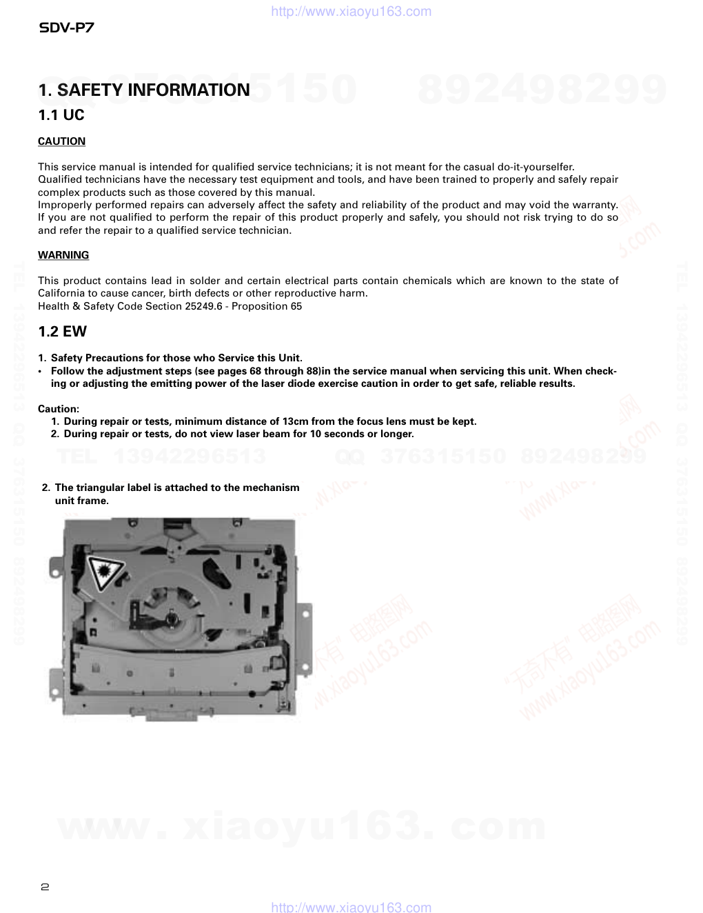
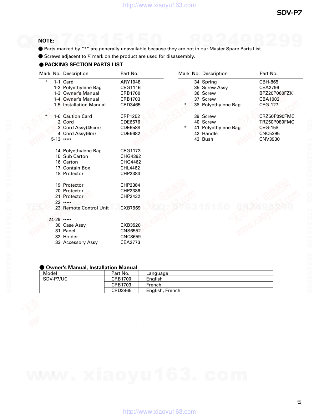
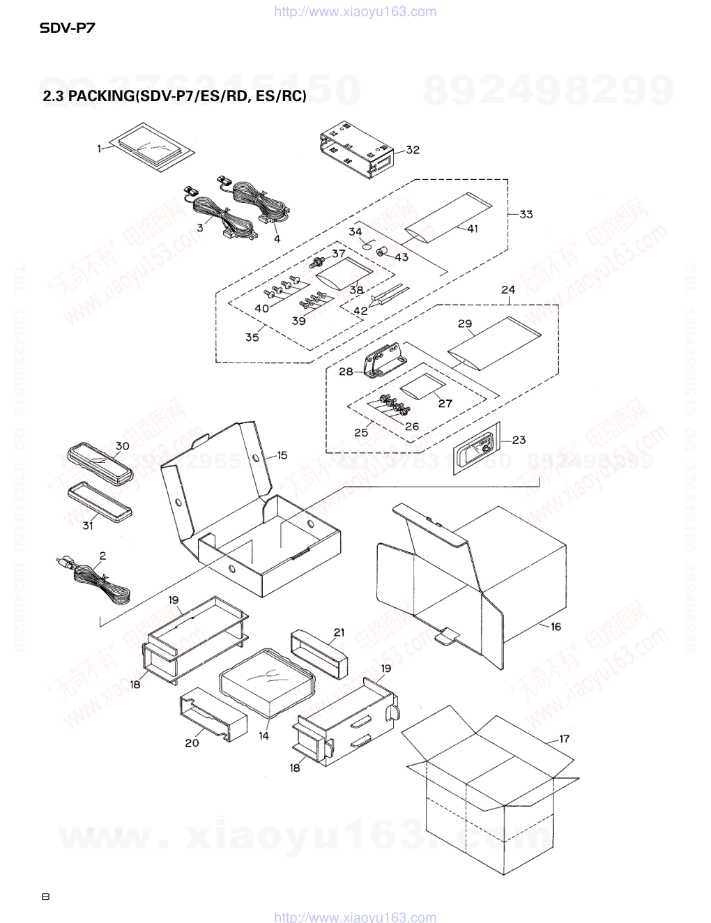
先锋PIONEER SDV-P7电路图
 "先锋PIONEER SDV-P7电路图-0")
 "先锋PIONEER SDV-P7电路图-1")
 "先锋PIONEER SDV-P7电路图-2")
 "先锋PIONEER SDV-P7电路图-3")
 "先锋PIONEER SDV-P7电路图-4")
 "先锋PIONEER SDV-P7电路图-5")
 "先锋PIONEER SDV-P7电路图-6")
 "先锋PIONEER SDV-P7电路图-7")
 "先锋PIONEER SDV-P7电路图-8")
 "先锋PIONEER SDV-P7电路图-9")
PIONEER CORPORATION 4-1, Meguro 1-Chome, Meguro-ku, Tokyo 153-8654, Japan PIONEER ELECTRONICS SERVICE INC. P.O.Box 1760, Long Beach, CA 90801-1760 U.S.A. PIONEER EUROPE NV Haven 1087 Keetberglaan 1, 9120 Melsele, Belgium PIONEER ELECTRONICS ASIACENTRE PTE.LTD. 253 Alexandra Road, #04-01, Singapore 159936 C PIONEER CORPORATION 2001 K-ZZA. MAY 2001 Printed in Japan ORDER NO. CRT2688 DVD PLAYER SDV-P7 UC,EW,ES/RC,ES/RD Service Manual - This service manual should be used together with the following manual(s): Model No. Order No. Mech. Module Remarks CX-954 CRT2670 MS2 DVD Mech. module:Circuit Description, Mech.Description, Disassembly CONTENTS 1. SAFETY INFORMATION ............................................2 2. EXPLODED VIEWS AND PARTS LIST.......................4 3. BLOCK DIAGRAM AND SCHEMATIC DIAGRAM ...18 4. PCB CONNECTION DIAGRAM ................................46 5. ELECTRICAL PARTS LIST ........................................58 6. ADJUSTMENT..........................................................67 7. GENERAL INFORMATION .......................................89 7.1 DIAGNOSIS ........................................................89 7.1.1 DISASSEMBLY .........................................89 7.1.2 CONNECTOR FUNCTION DESCRIPTION.......91 7.2 PARTS .................................................................92 7.2.1 IC................................................................92 7.2.2 DISPLAY..................................................107 7.3 OPERATIONAL FLOW CHART.........................108 8. OPERATIONS AND SPECIFICATIONS...................109 SDV-P7/UC - Manufactured under license from Dolby Laboratories. "Dolby" and the double-D symbol are trademarks of Dolby Laboratories. - DVD Player Service Precautions 1. Never adjust the LD VR in the pickup unit to protect the pickup from electrical damages. 2. For pickup unit(service)(CXX1530) handling, please refer to"Disassembly"(see page 89). During replacement, handling precautions shall be taken to prevent an electrostatic discharge(set the short switch of the pickup unit to the SHORT side). 3. During disassembly, be sure to turn the power off since an internal IC might be destroyed when a connector is plugged or unplugged. 4. Please adjusting the skew after changing the pickup unit(see page 71). www. xiaoyu163. com QQ 376315150 9 9 2 8 9 4 2 9 8 TEL 13942296513 9 9 2 8 9 4 2 9 8 0 5 1 5 1 3 6 7 3 Q Q TEL 13942296513 QQ 376315150 892498299 TEL 13942296513 QQ 376315150 892498299 http://www.xiaoyu163.com 2 SDV-P7 1. SAFETY INFORMATION 1.1 UC CAUTION This service manual is intended for qualified service technicians; it is not meant for the casual do-it-yourselfer. Qualified technicians have the necessary test equipment and tools, and have been trained to properly and safely repair complex products such as those covered by this manual. Improperly performed repairs can adversely affect the safety and reliability of the product and may void the warranty. If you are not qualified to perform the repair of this product properly and safely, you should not risk trying to do so and refer the repair to a qualified service technician. WARNING This product contains lead in solder and certain electrical parts contain chemicals which are known to the state of California to cause cancer, birth defects or other reproductive harm. Health & Safety Code Section 25249.6 - Proposition 65 1.2 EW 1. Safety Precautions for those who Service this Unit. • Follow the adjustment steps (see pages 68 through 88)in the service manual when servicing this unit. When check- ing or adjusting the emitting power of the laser diode exercise caution in order to get safe, reliable results. Caution: 1. During repair or tests, minimum distance of 13cm from the focus lens must be kept. 2. During repair or tests, do not view laser beam for 10 seconds or longer. 2. The triangular label is attached to the mechanism unit frame. www. xiaoyu163. com QQ 376315150 9 9 2 8 9 4 2 9 8 TEL 13942296513 9 9 2 8 9 4 2 9 8 0 5 1 5 1 3 6 7 3 Q Q TEL 13942296513 QQ 376315150 892498299 TEL 13942296513 QQ 376315150 892498299 http://www.xiaoyu163.com 3 SDV-P7 On the top of the player. CAUTION : VORSICHT : ADVARSEL : VARNING : VARO! : VISIBLE AND INVISIBLE LASER RADIATION WHEN OPEN. AVOID EXPOSURE TO BEAM. SICHTBARE UND UNSICHTBARE LASERSTRAHLUNG, WENN ABDECKUNG GEÖFFNET NICHT DEM STRAHL AUSSETZEN! SYNLIG OG USYNLIG LASERSTRÅLING VED ÅBNING UNDGÅ UDSÆTTELSE FOR STRÀLING. SYNLIG OCH OSYNLIG LASERSTRÅLNING NÄR DENNA DEL ÄR ÖPPNAD BETRAKTA EJ STRÅLEN. AVATTAESSA ALTISTUT NÄKYVÄ JA NÄKYMÄTTÖMÄLLE LASERSATEIL YLLE. ÄLÄ KATSO SÄTEESEN. VRW1699 CLASS 1 LASER PRODUCT WARNING! The AEL (accessible emission level )of the laser power output is less than CLASS 1 but the laser component is capable of emitting radiation exceeding the limit for CLASS 1. A specially instructed person should do servicing operation of the apparatus. Laser diode characteristics Wave length: DVD:640~660nm CD:770~810nm Maximum output:2.44mw(Emitting period :9sec.) DVD:743mw(Emitting period : unlimited) Additionla Laser Caution Transistors Q1104 and Q1108 in PCB drive the laser diodes for DVD and CD respectively. When Q1104 or Q1108 is shorted between their terminals, the laser diodes for DVD or CD will radiate beam. If the top cover is removed with no disc loaded while such short-circuit is continued, the naked eyes may be exposed to the laser beam. www. xiaoyu163. com QQ 376315150 9 9 2 8 9 4 2 9 8 TEL 13942296513 9 9 2 8 9 4 2 9 8 0 5 1 5 1 3 6 7 3 Q Q TEL 13942296513 QQ 376315150 892498299 TEL 13942296513 QQ 376315150 892498299 http://www.xiaoyu163.com 4 SDV-P7 2.1 PACKING(SDV-P7/UC) 2. EXPLODED VIEWS AND PARTS LIST www. xiaoyu163. com QQ 376315150 9 9 2 8 9 4 2 9 8 TEL 13942296513 9 9 2 8 9 4 2 9 8 0 5 1 5 1 3 6 7 3 Q Q TEL 13942296513 QQ 376315150 892498299 TEL 13942296513 QQ 376315150 892498299 http://www.xiaoyu163.com 5 SDV-P7 * 1-1 Card ARY1048 1-2 Polyethylene Bag CEG1116 1-3 Owner’s Manual CRB1700 1-4 Owner’s Manual CRB1703 1-5 Installation Manual CRD3465 * 1-6 Caution Card CRP1252 2 Cord CDE6576 3 Cord Assy(45cm) CDE6588 4 Cord Assy(6m) CDE6682 5-13 ••••• 14 Polyethylene Bag CEG1173 15 Sub Carton CHG4392 16 Carton CHG4462 17 Contain Box CHL4462 18 Protector CHP2383 19 Protector CHP2384 20 Protector CHP2386 21 Protector CHP2432 22 ••••• 23 Remote Control Unit CXB7969 24-29 ••••• 30 Case Assy CXB3520 31 Panel CNS6552 32 Holder CNC8659 33 Accessory Assy CEA2773 34 Spring CBH-865 35 Screw Assy CEA2796 36 Screw BPZ20P060FZK 37 Screw CBA1002 * 38 Polyethylene Bag CEG-127 39 Screw CRZ50P090FMC 40 Screw TRZ50P080FMC * 41 Polyethylene Bag CEG-158 42 Handle CNC5395 43 Bush CNV3930 Mark No. Description Part No. Mark No. Description Part No. - PACKING SECTION PARTS LIST NOTE: - Parts marked by “*” are generally unavailable because they are not in our Master Spare Parts List. - Screws adjacent to ∇ mark on the product are used for disassembly. - Owner's Manual, Installation Manual Model Part No. Language SDV-P7/UC CRB1700 English CRB1703 French CRD3465 English, French www. xiaoyu163. com QQ 376315150 9 9 2 8 9 4 2 9 8 TEL 13942296513 9 9 2 8 9 4 2 9 8 0 5 1 5 1 3 6 7 3 Q Q TEL 13942296513 QQ 376315150 892498299 TEL 13942296513 QQ 376315150 892498299 http://www.xiaoyu163.com 6 SDV-P7 2.2 PACKING(SDV-P7/EW) www. xiaoyu163. com QQ 376315150 9 9 2 8 9 4 2 9 8 TEL 13942296513 9 9 2 8 9 4 2 9 8 0 5 1 5 1 3 6 7 3 Q Q TEL 13942296513 QQ 376315150 892498299 TEL 13942296513 QQ 376315150 892498299 http://www.xiaoyu163.com 7 SDV-P7 1-1 Polyethylene Bag CEG1116 1-2 Owner’s Manual CRB1700 1-3 Owner’s Manual CRB1701 1-4 Owner’s Manual CRB1702 1-5 Owner’s Manual CRB1703 1-6 Owner’s Manual CRB1704 1-7 Owner’s Manual CRB1705 1-8 Installation Manual CRD3464 * 1-9 Caution Card CRP1251 * 1-10 Caution Card CRP1252 * 1-11 Warranty Card CRY1157 2 Cord CDE6576 3 Cord Assy(45cm) CDE6588 4 Cord Assy(6m) CDE6682 5 Accessory Assy CEA1917 6 Screw CBA1284 7 Handle CNC5395 8 Bush CNV1009 * 9 Polyethylene Bag E36-615 10 Screw Assy CEA1926 * 11 Polyethylene Sheet CNM5157 12 Screw CRZ50P090FMC 13 Screw TRZ50P080FMC 14 Polyethylene Bag CEG-162 15 Sub Carton CHG4392 16 Carton CHG4396 17 Contain Box CHL4396 18 Protector CHP2383 19 Protector CHP2384 20 Protector CHP2386 21 Protector CHP2432 22 Remote Sensor Assy CXB7618 23 Remote Control Unit CXB7969 24 Accessory Assy CEA2827 25 Screw Assy CEA2938 26 Screw(M6x16) CBA1295 * 27 Polyethylene Bag E36-613 28 Angle CNC9520 * 29 Polyethylene Bag E36-637 30 Case Assy CXB3520 31 Panel CNS6552 32 Holder CNC8659 Mark No. Description Part No. Mark No. Description Part No. - PACKING SECTION PARTS LIST - Owner's Manual, Installation Manual Model Part No. Language SDV-P7/EW CRB1700 English CRB1701 Spanish CRB1702 German CRB1703 French CRB1704 Italian CRB1705 Dutch CRD3464 English, Spanish, French, German, Italian, Dutch www. xiaoyu163. com QQ 376315150 9 9 2 8 9 4 2 9 8 TEL 13942296513 9 9 2 8 9 4 2 9 8 0 5 1 5 1 3 6 7 3 Q Q TEL 13942296513 QQ 376315150 892498299 TEL 13942296513 QQ 376315150 892498299 http://www.xiaoyu163.com 8 SDV-P7 2.3 PACKING(SDV-P7/ES/RD, ES/RC) www. xiaoyu163. com QQ 376315150 9 9 2 8 9 4 2 9 8 TEL 13942296513 9 9 2 8 9 4 2 9 8 0 5 1 5 1 3 6 7 3 Q Q TEL 13942296513 QQ 376315150 892498299 TEL 13942296513 QQ 376315150 892498299 http://www.xiaoyu163.com 9 SDV-P7 1-1 Polyethylene Bag CEG1116 1-2 Owner’s Manual CRB1700 1-3 Installation Manual(ES/RD) CRB1738 Installation Manual(ES/RC) CRD3466 * 1-4 Caution Card CRP1252 1-5 Owner’s Manual(ES/RC) CRB1706 2 Cord CDE6576 3 Cord Assy(45cm) CDE6588 4 Cord Assy(6m) CDE6682 5-13 ••••• 14 Polyethylene Bag CEG-162 15 Sub Carton CHG4392 16 Carton(ES/RD) CHG4464 Carton(ES/RC) CHG4463 17 Contain Box(ES/RD) CHL4464 Contain Box(ES/RC) CHL4463 18 Protector CHP2383 19 Protector CHP2384 20 Protector CHP2386 21 Protector CHP2432 22 ••••• 23 Remote Control Unit CXB7969 24 Accessory Assy CEA2828 25 Screw Assy CEA2938 26 Screw(M6x16) CBA1295 * 27 Polyethylene Bag E36-613 28 Angle CNC9521 * 29 Polyethylene Bag E36-637 30 Case Assy CXB3520 31 Panel CNS6553 32 Holder CNC8659 33 Accessory Assy CEA2002 34 Spring CBH-865 35 Screw Assy CEA2003 36 ••••• 37 Screw CBA1284 * 38 Polyethylene Bag CEG-127 39 Screw CRZ50P090FMC 40 Screw TRZ50P080FMC * 41 Polyethylene Bag CEG-158 42 Handle CNC5395 43 Bush CNV1009 Mark No. Description Part No. Mark No. Description Part No. - PACKING SECTION PARTS LIST - Owner's Manual, Installation Manual Model Part No. Language SDV-P7/ES/RC CRB1700 English CRB1706 Chinese CRD3466 English, Chinese - Owner's Manual, Installation Manual Model Part No. Language SDV-P7/ES/RD CRB1700 English CRB1738 English www. xiaoyu163. com QQ 376315150 9 9 2 8 9 4 2 9 8 TEL 13942296513 9 9 2 8 9 4 2 9 8 0 5 1 5 1 3 6 7 3 Q Q TEL 13942296513 QQ 376315150 892498299 TEL 13942296513 QQ 376315150 892498299 http://www.xiaoyu163.com 10 SDV-P7 2.4 EXTERIOR(SDV-P7/UC) A C B A C B 70 71 83 89 90 91 85 87 73 76 34 30 41 23 1 1 3 3 31 18 18 19 17 33 20 36 93 21 29 35 28 32 27 24 16 37 37 25 22 26 75 74 92 44 77 80 88 43 79 78 86 84 82 72 72 81 45-2 72 56 59 49 47 47 50 51 55 54 48 64 3 46 52 62 65 69 66 46 46 46 15 4 11 5 68 63 42 96 58 67 45-1 61 53 60 57 72 38 40 39 98 97 10 4 4 4 9 2 2 4 94 95 70 6 8 7 14 12 13 A B C D E www. xiaoyu163. com QQ 376315150 9 9 2 8 9 4 2 9 8 TEL 13942296513 9 9 2 8 9 4 2 9 8 0 5 1 5 1 3 6 7 3 Q Q TEL 13942296513 QQ 376315150 892498299 TEL 13942296513 QQ 376315150 892498299 http://www.xiaoyu163.com 11 SDV-P7 1 Screw BMZ30P040FZK 2 Screw BSZ26P060FMC 3 Screw BSZ30P060FMC 4 Screw(M2x2.2) CBA1419 5 Transistor(Q907) 2SD2396 6 Cord Assy CDE6588 7 Fuse(4A) CEK1001 8 Cap CNS1472 9 Cable CDE6600 10 Cord CDE6601 11 Cord Assy CDE6606 12 Cord Assy CDE6682 13 Fuse(4A) CEK1001 14 Cap CNS1472 15 Cord Assy CDE6721 16 Button(EJECT) CAC6839 17 Screw(M2x2) CBA1176 18 Washer CBF1038 19 Washer CBF1039 20 Spring CBH2428 21 Spring CBH2429 22 Spring CBL1512 23 Holder CNC9096 24 Cover CNM6854 25 Panel CNS6278 26 Pin CNV6486 27 Lighting Conductor CNV6487 28 Gear CNV6507 29 Arm CNV6508 30 Panel PCB Unit CWM7887 31 Socket(CN851) CKS3550 32 Connector(CN852) CKS4462 33 Damper Unit CXB5070 34 Holder Unit CXB6357 35 Clutch Unit CXB6358 36 Holder Unit CXB7506 37 Screw IMS20P045FZK 38 Case CNB2672 39 Bracket CNC9396 40 Bracket CNC9397 41 Insulator CNM7258 42 Sheet CNM7457 43 IC(IC861) TSOP1840SB1 44 Panel CNS6552 45 Audio Control Unit CWM7684 46 Screw BSZ26P060FMC 47 Clamper CEF1008 48 Pin Jack(CN202) CKB1049 49 Plug(CN901) CKS-461 * 50 Plug(CN701) CKS-792 51 Plug(CN101) CKS1043 52 Connector(CN304) CKS2104 53 Connector(CN301) CKS3124 54 Pin Jack(CN161) CKS3144 55 Connector(CN102) CKS3408 56 Plug(CN801) CKS3537 57 Connector(CN601) CKS3814 58 Connector(CN203) CKS3902 59 Connector(CN201) CKS4052 60 Connector(CN702) CKS4362 61 Connector(CN204) CKS4496 62 Connector(CN302) CKS4533 63 Panel CNB2673 64 Holder CNC9392 65 Holder CNC9393 66 Holder CNC9394 67 Holder CNC9502 68 Heat Sink CNC9518 69 Connector(CN303) HKS-193 70 Resistor RS1/2PMF102J 71 Grille Panel Assy CXB8306 72 Screw BPZ20P100FZK 73 Button(OPEN) CAC6780 74 Button(POWER) CAC6989 75 Button(PLAY/PAUSE, STOP) CAC6990 76 Button(+,-) CAC6991 * 77 Badge CAH1754 78 Spring CBH2430 79 Spring CBH2431 80 Spring CBH2491 81 Cover CNS6282 82 Holder CNV6505 83 Holder CNV6506 84 Keyboard Unit CWM7888 85 LCD CAW1687 86 Connector(CN861) CKS4524 87 Holder CNC9395 88 Cushion CNM7260 89 Spacer CNM7585 90 Rubber CNV6708 91 Lighting Conductor CNV6709 92 Grille Unit CXB7539 93 Chassis Unit CXB7243 94 Remote Control Unit CXB7969 95 Cover CZN5357 96 DVD Mechanism Module(MS2) CXK6111 97 Insulator CNM7533 98 Ferrite CTX1086 - EXTERIOR SECTION PARTS LIST Mark No. Description Part No. Mark No. Description Part No. www. xiaoyu163. com QQ 376315150 9 9 2 8 9 4 2 9 8 TEL 13942296513 9 9 2 8 9 4 2 9 8 0 5 1 5 1 3 6 7 3 Q Q TEL 13942296513 QQ 376315150 892498299 TEL 13942296513 QQ 376315150 892498299 http://www.xiaoyu163.com 12 SDV-P7 A C B A C B 70 71 83 89 90 91 85 87 73 76 34 30 41 23 1 1 3 3 31 18 18 19 17 33 20 36 93 21 29 35 28 32 27 24 16 37 37 25 22 26 75 74 92 44 77 80 88 43 79 78 86 84 82 72 72 81 45-2 72 56 59 49 47 47 50 51 55 54 48 64 3 46 52 62 65 69 66 46 46 46 15 4 11 5 68 63 42 96 58 67 45-1 61 53 60 57 72 38 40 39 98 97 10 4 4 4 9 2 2 4 94 95 70 6 8 7 14 12 13 A B C D E 2.5 EXTERIOR(SDV-P7/EW) www. xiaoyu163. com QQ 376315150 9 9 2 8 9 4 2 9 8 TEL 13942296513 9 9 2 8 9 4 2 9 8 0 5 1 5 1 3 6 7 3 Q Q TEL 13942296513 QQ 376315150 892498299 TEL 13942296513 QQ 376315150 892498299 http://www.xiaoyu163.com SDV-P7 1 Screw BMZ30P040FZK 2 Screw BSZ26P060FMC 3 Screw BSZ30P060FMC 4 Screw(M2x2.2) CBA1419 5 Transistor(Q907) 2SD2396 6 Cord Assy CDE6588 7 Fuse(4A) CEK1001 8 Cap CNS1472 9 Cable CDE6600 10 Cord CDE6601 11 Cord Assy CDE6606 12 Cord Assy CDE6682 13 Fuse(4A) CEK1001 14 Cap CNS1472 15 Cord Assy CDE6721 16 Button(EJECT) CAC6839 17 Screw(M2x2) CBA1176 18 Washer CBF1038 19 Washer CBF1039 20 Spring CBH2428 21 Spring CBH2429 22 Spring CBL1512 23 Holder CNC9096 24 Cover CNM6854 25 Panel CNS6278 26 Pin CNV6486 27 Lighting Conductor CNV6487 28 Gear CNV6507 29 Arm CNV6508 30 Panel PCB Unit CWM7887 31 Socket(CN851) CKS3550 32 Connector(CN852) CKS4462 33 Damper Unit CXB5070 34 Holder Unit CXB6357 35 Clutch Unit CXB6358 36 Holder Unit CXB7506 37 Screw IMS20P045FZK 38 Case CNB2672 39 Bracket CNC9396 40 Bracket CNC9397 41 Insulator CNM7258 42 Sheet CNM7457 43 IC(IC861) TSOP1840SB1 44 Panel CNS6552 45 Audio Control Unit CWM7683 46 Screw BSZ26P060FMC 47 Clamper CEF1008 48 Pin Jack(CN202) CKB1049 49 Plug(CN901) CKS-461 * 50 Plug(CN701) CKS-792 51 Plug(CN101) CKS1043 52 Connector(CN304) CKS2104 53 Connector(CN301) CKS3124 54 Pin Jack(CN161) CKS3144 55 Connector(CN102) CKS3408 56 Plug(CN801) CKS3537 57 Connector(CN601) CKS3814 58 Connector(CN203) CKS3902 59 Connector(CN201) CKS4052 60 Connector(CN702) CKS4362 61 Connector(CN204) CKS4496 62 Connector(CN302) CKS4533 63 Panel CNB2673 64 Holder CNC9392 65 Holder CNC9393 66 Holder CNC9394 67 Holder CNC9502 68 Heat Sink CNC9518 69 Connector(CN303) HKS-193 70 Resistor RS1/2PMF102J 71 Grille Panel Assy CXB8305 72 Screw BPZ20P100FZK 73 Button(OPEN) CAC6780 74 Button(POWER) CAC6989 75 Button(PLAY/PAUSE, STOP) CAC6990 76 Button(+,-) CAC6991 * 77 Badge CAH1754 78 Spring CBH2430 79 Spring CBH2431 80 Spring CBH2491 81 Cover CNS6282 82 Holder CNV6505 83 Holder CNV6506 84 Keyboard Unit CWM7888 85 LCD CAW1687 86 Connector(CN861) CKS4524 87 Holder CNC9395 88 Cushion CNM7260 89 Spacer CNM7585 90 Rubber CNV6708 91 Lighting Conductor CNV6709 92 Grille Unit CXB7538 93 Chassis Unit CXB7242 94 Remote Control Unit CXB7969 95 Cover CZN5357 96 DVD Mechanism Module(MS2) CXK6111 97 Insulator CNM7533 98 Ferrite CTX1086 - EXTERIOR SECTION PARTS LIST Mark No. Description Part No. Mark No. Description Part No. 13 www. xiaoyu163. com QQ 376315150 9 9 2 8 9 4 2 9 8 TEL 13942296513 9 9 2 8 9 4 2 9 8 0 5 1 5 1 3 6 7 3 Q Q TEL 13942296513 QQ 376315150 892498299 TEL 13942296513 QQ 376315150 892498299 http://www.xiaoyu163.com 14 SDV-P7 2.6 EXTERIOR(SDV-P7/ES/RD,/ES/RC) A C B A C B 70 71 83 89 90 91 85 87 73 76 34 30 41 23 1 1 3 3 31 18 18 19 17 33 20 36 93 21 29 35 28 32 27 24 16 37 37 25 22 26 75 74 92 44 77 80 88 43 79 78 86 84 82 72 72 81 45-2 72 56 59 49 47 47 50 51 55 54 48 64 3 46 52 62 65 69 66 46 46 46 15 4 11 5 68 63 42 96 58 67 45-1 61 53 60 57 72 38 40 39 98 97 10 4 4 4 9 2 2 4 94 95 70 6 8 7 14 12 13 A B C D E www. xiaoyu163. com QQ 376315150 9 9 2 8 9 4 2 9 8 TEL 13942296513 9 9 2 8 9 4 2 9 8 0 5 1 5 1 3 6 7 3 Q Q TEL 13942296513 QQ 376315150 892498299 TEL 13942296513 QQ 376315150 892498299 http://www.xiaoyu163.com 15 SDV-P7 1 Screw BMZ30P040FZK 2 Screw BSZ26P060FMC 3 Screw BSZ30P060FMC 4 Screw(M2x2.2) CBA1419 5 Transistor(Q907) 2SD2396 6 Cord Assy CDE6588 7 Fuse(4A) CEK1001 8 Cap CNS1472 9 Cable CDE6600 10 Cord CDE6601 11 Cord Assy CDE6606 12 Cord Assy CDE6682 13 Fuse(4A) CEK1001 14 Cap CNS1472 15 Cord Assy CDE6721 16 Button(EJECT) CAC6839 17 Screw(M2x2) CBA1176 18 Washer CBF1038 19 Washer CBF1039 20 Spring CBH2428 21 Spring CBH2429 22 Spring CBL1512 23 Holder CNC9096 24 Cover CNM6854 25 Panel CNS6278 26 Pin CNV6486 27 Lighting Conductor CNV6487 28 Gear CNV6507 29 Arm CNV6508 30 Panel PCB Unit CWM7887 31 Socket(CN851) CKS3550 32 Connector(CN852) CKS4462 33 Damper Unit CXB5070 34 Holder Unit CXB6357 35 Clutch Unit CXB6358 36 Holder Unit CXB7506 37 Screw IMS20P045FZK 38 Case CNB2693 39 Bracket CNC9396 40 Bracket CNC9397 41 Insulator CNM7258 42 Sheet CNM7457 43 IC(IC861) TSOP1840SB1 44 Panel CNS6553 45 Audio Control Unit(ES/RD) CWM7686 Audio Control Unit(ES/RC) CWM7685 46 Screw BSZ26P060FMC 47 Clamper CEF1008 48 Pin Jack(CN202) CKB1049 49 Plug(CN901) CKS-461 * 50 Plug(CN701) CKS-792 51 Plug(CN101) CKS1043 52 Connector(CN304) CKS2104 53 Connector(CN301) CKS3124 54 Pin Jack(CN161) CKS3144 55 Connector(CN102) CKS3408 56 Plug(CN801) CKS3537 57 Connector(CN601) CKS3814 58 Connector(CN203) CKS3902 59 Connector(CN201) CKS4052 60 Connector(CN702) CKS4362 61 Connector(CN204) CKS4496 62 Connector(CN302) CKS4533 63 Panel CNB2673 64 Holder CNC9392 65 Holder CNC9393 66 Holder CNC9394 67 Holder CNC9502 68 Heat Sink CNC9518 69 Connector(CN303) HKS-193 70 Resistor RS1/2PMF102J 71 Grille Panel Assy(ES/RD) CXB8308 Grille Panel Assy(ES/RC) CXB8307 72 Screw BPZ20P100FZK 73 Button(OPEN) CAC6780 74 Button(POWER) CAC6989 75 Button(PLAY/PAUSE, STOP) CAC6990 76 Button(+,-) CAC6991 * 77 Badge CAH1754 78 Spring CBH2430 79 Spring CBH2431 80 Spring CBH2491 81 Cover CNS6282 82 Holder CNV6505 83 Holder CNV6506 84 Keyboard Unit CWM7888 85 LCD CAW1687 86 Connector(CN861) CKS4524 87 Holder CNC9395 88 Cushion CNM7260 89 Spacer CNM7585 90 Rubber CNV6708 91 Lighting Conductor CNV6709 92 Grille Unit CXB7540 93 Chassis Unit CXB7620 94 Remote Control Unit CXB7969 95 Cover CZN5357 96 DVD Mechanism Module(MS2) CXK6111 97 Insulator CNM7533 98 Ferrite CTX1086 - EXTERIOR SECTION PARTS LIST Mark No. Description Part No. Mark No. Description Part No. www. xiaoyu163. com QQ 376315150 9 9 2 8 9 4 2 9 8 TEL 13942296513 9 9 2 8 9 4 2 9 8 0 5 1 5 1 3 6 7 3 Q Q TEL 13942296513 QQ 376315150 892498299 TEL 13942296513 QQ 376315150 892498299 http://www.xiaoyu163.com 16 SDV-P7 2.7 DVD MECHANISM MODULE F www. xiaoyu163. com QQ 376315150 9 9 2 8 9 4 2 9 8 TEL 13942296513 9 9 2 8 9 4 2 9 8 0 5 1 5 1 3 6 7 3 Q Q TEL 13942296513 QQ 376315150 892498299 TEL 13942296513 QQ 376315150 892498299 http://www.xiaoyu163.com 17 SDV-P7 1 DVD core unit V CWX2574 2 Terminal(CN1703) CKF1065 3 Terminal(CN1705) CKF1065 4 Terminal(CN1706) CKF1065 5 Connector(CN1100) CKS3749 6 Connector(CN1701) CKS4052 7 Connector(CN1700) CKS4374 8 Connector(CN1300) CKS4507 9 Screw(M2x3) CBA1486 10 Screw CBA1535 11 Screw(M2x2.2) CBA1547 12 Screw(M2x2.2) CBA1548 13 Screw(M1.4x2) CBA1549 14 Damper CNV6927 15 Washer CBF1038 16 Spring CBH2394 17 Spring CBH2395 18 Spring CBH2396 19 Spring CBH2397 20 Spring CBH2398 21 Spring CBH2399 22 Spring CBH2400 23 Spring CBH2401 24 Spring CBH2402 25 Spring CBH2403 26 Spring CBH2404 27 Spring CBH2405 28 Spring CBH2406 29 Spring CBH2407 30 Spring CBH2408 31 Spring CBH2410 32 Spring CBH2411 33 Spring CBH2413 34 Spring CBH2414 35 Spring CBL1499 36 Spring CBL1500 37 Sheet CNM7590 38 Pickup Unit(Service)(DP4)CXX1530 39 Shaft CLA3878 40 Shaft CLA3879 41 Shaft CLA3881 42 Lever CNC8988 43 Bracket CNC8992 44 Arm CNC8994 45 Sheet CNM6883 46 Sheet CNM6884 47 PCB CNP5971 48 Ball CNR1189 49 Guide CNV6352 50 Guide CNV6353 51 Guide CNV6354 52 Guide CNV6355 53 Guide CNV6356 54 Clamper CNV6357 55 Arm CNV6358 56 Gear CNV6361 57 Gear CNV6362 58-61 ••••• 62 Rack CNV6367 63 Damper CNV6368 64 Arm CNV6369 65 Arm CNV6370 66 Gear CNV6372 67 Holder CNV6374 68 Rack CNV6376 69 Arm CNV6377 70 Arm CNV6378 71 Arm CNV6379 72 Gear Unit CXB5959 73 Holder CNV6383 74 Guide CNV6384 75 Holder CNV6385 76 Lever Unit CXB5943 77 Holder Unit CXB5944 * 78 Holder Unit CXB5947 79 Frame Unit CXB5948 80 Frame Unit CXB5949 81 Arm Unit CXB5950 82 Arm Unit CXB5951 83 Arm Unit CXB5952 84 Chassis Unit CXB5953 85 Arm Unit CXB5954 86 Motor Unit(CRG) CXB5955 87 Screw Unit CXB5957 88 Roller Unit CXB5958 89 Washer CBF1060 90 Spring CBH2170 91 Roller CNV6068 92 Holder CNV6210 93 Washer YE20FUC 94 Motor Unit(LOAD) CXB5960 95 Motor Unit(SPDL) CXB6218 96 Washer YE15FUC 97 Screw IMS20P030FMC * 98 Shaft CLA3877 * 99 Gear CNV6359 * 100 Caller CNV6382 * 101 Arm Unit CXB5945 102 Cover CNC9532 103 Washer CBF1087 104 Roller CNV6928 105 Shaft CLA4091 106 Shaft CLA4092 107 Guide CNV6805 108 Connector(CN1702) CKS4282 109 Screw (M2x3.5) CBA1560 110 Screw (M2x2.2) CBA1419 Mark No. Description Part No. Mark No. Description Part No. - DVD MECHANISM MODULE SECTION PARTS LIST www. xiaoyu163. com QQ 376315150 9 9 2 8 9 4 2 9 8 TEL 13942296513 9 9 2 8 9 4 2 9 8 0 5 1 5 1 3 6 7 3 Q Q TEL 13942296513 QQ 376315150 892498299 TEL 13942296513 QQ 376315150 892498299 http://www.xiaoyu163.com 18 SDV-P7 1 2 3 4 1 2 3 4 D C B A CN801 CN852 CN851 CN861 ILM+B 11 REMOTE 5 FLPILM+B 13 LCDEN 1 LCDCLK 3 LCDDT 4 LCDCS 2 KEYDT1 7 csens 10 11 5 13 KEYDT0 6 9 5 1 3 6 2 4 10 4 8 6 10 reset reset/FlASH ILM+B REMOTE LCDINH LCDCLK LCDDATA LCDCE KEYDT1 CSENS RESET 12 12 2 11 VIDEO5 Q915 Q921 Q918 Q931 Q917 Q930 Q929 Q913 Q914 SWVDD REMIN 45 SYSPW 21 DVSELL 26 91 csens 98 reset 11 IC 601 (1/2) PE5229A SYSTEM CONTROLLER MEMHLD 80 LEDCS 49 LEDEN 50 LEDCLK 48 KEYDT1 76 KEYDT0 75 LEDDT 47 Q908 MSVD 32 SWVDD IC 861 TSOP1840SB1 3 1 60 57 61 62 IC 862 LC75822W LCD DRIVER REMOTE CONTROL SENSOR 12 10 7 11 9 3 KEY MATRIX LCD SWVDD D872 D873 B KEYBOARD UNIT 1 3 4 2 7 C PANEL PCB UNIT E OPTICAL PCB IC 691 TC7W53FU IC 603 S-80734ANDYI 2 1 RESET VDD Q907 VD8V BU Q902 Q901 VDD BU CN601 CN302 CN304 CN303 CN301 6 8 7 5 CN702 Q701 Q702 Q703 Q605 VDD BZ601 PEE 100 MSMCVD 34 4 DVD3.3V Q Q SYSPW 21 CPU +3.3V IC 301 TC7W125FU 3 8 2 1 1 1 4 2 A AUDIO CONTROL PCB Q301 VDD Q302 Q905 BU IC 901 BA08SF SYSRE 1 Q906 VIDEO5 BU S851 EJECT 12 1 8 7 6 8 SWVDD 9 9 8 5 SWVDD VDD 1 ILMPW2 1 3 3 SRAM+3.3V MSMVD 33 14 14 SWVDD 30 28 F DVD CORE UNIT V Q1104 Q1108 Q1105 Q1107 Q1102 65LD 78LD 2 41 4 VSHF Q1109 LCDSG1 Q1110 LCDSG2 Q1111 LCDSG3 CN1100 CN1300 LPC01 RFENV LPC02 5 7 IC 1101 NJM2904M IC 1704 TC74VCX08FT IC 1701 M5M5V216ATP-70HI IC1702 PD6354B FEP IC 1100 AN8702FH ODC IC 1400 MNZS25BDAUB ADSC IC 1200 MN677061ZYUB 59 XWR 100 MCK33 10 12 11 13 8 11 30 124 99 110 33 5 2 3 3 CPU IC 1700 PE5277A 62 63 78 90 X1700 5MHz X2ENV CLKOUT 94 23 36 33 117 6 17 1 2 3 11 116 86 107 59 104 2 4 2 1 4 2 2 1 1 1 97 71 83 79 96 105 CD/DVD X2 X1 XWR BUSISO XRES XCSSRAM FSSW VCONTA VCONTB XUWR DISCDET TILT1 TILT2 TILT3 AVREF ADENA DSCSNS Q1700 S1301 S1303 S1304 S1302 IC 1705 TC7SH04FU IC 1706 TC7SH32FU IC 1509 TC74VCX74FT IC 1503 TC74VCX74FT IC 1504 TC74VCX04FT SRAM FLASH MEMORY IC 1500 MSM56V16160F SDRAM IC 1403 TC74LCX2 IC 1405 TC7SH04FU IC 1506 SM8703A IC 1501 MSM56V16160F SDRAM IC 1802 BA033SFP IC 1804 BA00BC0WFP 2 IC 1803 BA18BC0WFP XBWR VGOUT CLK27 EXTCK HCLK 19 22 24 23 2 4 3 1 10 11 2 1 CLOCK G Q1600 Q1601 F1600 IC 1601 AK4380VT Q1602 AV CHIP IC 1502 MN677532JAUB IC 1300 BA5985FM VD63 27 6 7 8 PU UNIT(SERVICE)(DP4) A,B1-4,C,RF+,RF- M SPINDLE MOTOR M CARRIGE MOTOR M LOADING MOTOR FOP,FOM,TOP,TOM EC,CONT COP,COM DRIVER BLOCK 9 LOM 10 LOP CLAMP SW 12cm detect SW 8cm detect SW L/E ON/OFF SW GBAL, TBAL, FBAL Q EXTCK,SRCKAV,AOUT0,LRCKAV A0-17,D0-15 CTS,DTR,RXPC,TXPC,VPP, SOCOMN,SCKCOM 1 VCC33 4 VCC18 4 VCC27 4 85 IEC958 3. BLOCK DIAGRAM AND SCHEMATIC DIAGRAM 3.1 BLOCK DIAGRAM www. xiaoyu163. com QQ 376315150 9 9 2 8 9 4 2 9 8 TEL 13942296513 9 9 2 8 9 4 2 9 8 0 5 1 5 1 3 6 7 3 Q Q TEL 13942296513 QQ 376315150 892498299 TEL 13942296513 QQ 376315150 892498299 http://www.xiaoyu163.com 19 SDV-P7 5 6 7 8 5 6 7 8 D C B A CN702 6 3 10 11 12 4 Q701 Q702 Q703 Q605 DD AV BUS OUT CONNECTOR BZ601 IC 905 BA00ASFP 4 2 IC 903 BA5250-ADJ 6 1 3 D3.3V Q909 Q916 Q923 Q924 BU SYS+B Q911 Q912 CPU +3.3V DVD 3.3V Q919 Q920 BU SYS+B IC 901 BA08SFP SYSREG. 4 1 IC 601 (2/2) PE5229A SYSTEM CONTROLLER IC 202 NJM2246M 2 7 IC 204 BA7623F 2 3 4 7 6 IC 203 NJM2235M 7 IC 201 NJM2267M 1 5 Q161 BU RMUTE 27 DVSSEL 26 MUTE 28 DV5VSEL 25 bsens 93 Q104 BU Q163 Q107 Q108 Q164 FVIDEO RVIDEO RAL FL RAR 6 CN202 CN161 IC 101 NJM4558MD 1 7 IC 102 BA3131FS 20 9 3 18 1 14 7 CN101 6 FR 8 ASENB 7 BUS– 4 BUS+ 1 CN102 CN901 7 IC 103 TA2050F 13 1 8 BUSL+ 5 BUS– 1 BUS+ 8 ASENB 11 BUSL– 10 BUSR– BU ACC MASTER SLAVE (IP) 9 BUSR+ 15 10 12 IP-OUT IP-IN asens 92 PBSENS 30 MESN 69 Q602 S601 3 4 PB 2 Q603 CN201 VIDEOOUT 13 AUDIO Rch OUT TXD/RXD/DTR/CTS 29 IC 604 TC74VHCT08AFT VCONTB 18 6 4 AMUTE 19 D EXTENSION PCB CN204 CN203 EXTERNAL Q927 Q928 DAC+5V MSAMUTE 42 REMPW LED-V REMIN NEW AV SENS AVONOUT IPSEL1 +3.3V Q926 5 Q653 3 1 REAR MUTE VIDEO AUDIO VDD Q601 Q654 Q652 Q651 BU 4A AUDIO Lch OUT 26 5 3 8 2 COMP OUT 3 4 28 26 22 15 12 11 12 IC 1500 SM56V16160F8TKFM SDRAM IC 1403 TC74LCX244FT IC 1506 SM8703AV IC 1501 SM56V16160F8TKFM SDRAM 19 1 7 12 22 24 23 1 CLOCK GEN VCONTB VIDEO OUT Rch OUT Lch OUT AMUTE VCONTA Q1600 602 CN1700 CN1701 VCC33 VCC Q1603 PC,TXPC,VPP,SICOMN, OMN,SCKCOMN 1 1 CN1702 34 CN1701 DAC+5V 7 DAC+5V 6 SRAM+3.3V 5 CPU+3.3V 35 36 SRAM+3.3V CPU+3.3V 23 VCONTB www. xiaoyu163. com QQ 376315150 9 9 2 8 9 4 2 9 8 TEL 13942296513 9 9 2 8 9 4 2 9 8 0 5 1 5 1 3 6 7 3 Q Q TEL 13942296513 QQ 376315150 892498299 TEL 13942296513 QQ 376315150 892498299 http://www.xiaoyu163.com 20 SDV-P7 1 2 3 4 1 2 3 4 D C B A > > > > > CN1702 CN1701 C CN851 A AUDIO CONTROL PCB Audio Control Unit Consists of Audio Control PCB Extension PCB Optical PCB F 2/2 ILMPW2 V V V V V V V V V V V V V V V V V V V V V V V A A A A A A VIDEO LINE AUDIO LINE V White 100% 0.5Vp-p 2Vp-p 2Vp-p 1Vp-p 2Vp-p 2Vp-p CD(0dB) 3.2dBs A A-a 3.2 OVERALL CONNECTION DIAGRAM(GUIDE PAGE) Note: When ordering service parts, be sure to refer to “EXPLODED VIEWS AND PARTS LIST” or “ELECTRICAL PARTS LIST”. A-a A-b A-a A-b A-b A-a Large size SCH diagram Guide page Detailed page www. xiaoyu163. com QQ 376315150 9 9 2 8 9 4 2 9 8 TEL 13942296513 9 9 2 8 9 4 2 9 8 0 5 1 5 1 3 6 7 3 Q Q TEL 13942296513 QQ 376315150 892498299 TEL 13942296513 QQ 376315150 892498299 http://www.xiaoyu163.com 21 SDV-P7 5 6 7 8 5 6 7 8 D C B A A A-b M/S select SW R619 10K:UC 22K:EW 33K:ES/RC R618 33K:UC 22K:EW 47K:ES/RD 4A > > > > NEW AV IN CONNECTOR NEW AV OUT CONNECTOR E CN303 FRONT VIDEO REAR VIDEO Decimal points for resistor and capacitor fixed values are expressed as : 2.2 2R2 0.022 R022 ← ← The > mark found on some component parts indicates the importance of the safety factor of the part. Therefore, when replacing, be sure to use parts of identical designation. Symbol indicates a resistor. No differentiation is made between chip resistors and discrete resistors. NOTE : Symbol indicates a capacitor. No differentiation is made between chip capacitors and discrete capacitors. AUDIO OUT Lch AUDIO OUT Rch :The power supply is shown with the marked box. V V V V V V V V V V V A A A A A A A A A A A A A A A A 1Vp-p at 75Ω White 100% 1Vp-p 1Vp-p at 75Ω CD(0dB) 2.2dBs CD(0dB) 2.2dBs CD(0dB) 2.2dBs www. xiaoyu163. com QQ 376315150 9 9 2 8 9 4 2 9 8 TEL 13942296513 9 9 2 8 9 4 2 9 8 0 5 1 5 1 3 6 7 3 Q Q TEL 13942296513 QQ 376315150 892498299 TEL 13942296513 QQ 376315150 892498299 http://www.xiaoyu163.com 22 SDV-P7 1 2 3 4 1 2 3 4 D C B A > > CN1701 C CN851 A AUDIO CONTROL PCB Audio Control Unit Consists of Audio Control PCB Extension PCB Optical PCB ILMPW2 V V V V V V V V V V V V V V A A A VIDEO LINE AUDIO LINE V 2Vp-p 2Vp-p A-a A-b A-a 1 www. xiaoyu163. com QQ 376315150 9 9 2 8 9 4 2 9 8 TEL 13942296513 9 9 2 8 9 4 2 9 8 0 5 1 5 1 3 6 7 3 Q Q TEL 13942296513 QQ 376315150 892498299 TEL 13942296513 QQ 376315150 892498299 http://www.xiaoyu163.com 23 SDV-P7 5 6 7 8 5 6 7 8 D C B A A-a A-b A-a > > > CN1702 F 2/2 V V V V V V V V V V V V V V V V V V A A A White 100% 0.5Vp-p 2Vp-p 1Vp-p 2Vp-p p p CD(0dB) 3.2dBs 2 3 www. xiaoyu163. com QQ 376315150 9 9 2 8 9 4 2 9 8 TEL 13942296513 9 9 2 8 9 4 2 9 8 0 5 1 5 1 3 6 7 3 Q Q TEL 13942296513 QQ 376315150 892498299 TEL 13942296513 QQ 376315150 892498299 http://www.xiaoyu163.com 24 SDV-P7 1 2 3 4 1 2 3 4 D C B A > > NEW AV IN CONNECTOR NEW AV OUT CONNECTOR FRONT VIDEO REAR VIDEO Decimal points for resistor and capacitor fixed values are expressed as : 2.2 2R2 0.022 R022 ← ← The > mark found on some component parts indicates the importance of the safety factor of the part. Therefore, when replacing, be sure to use parts of identical designation. Symbol indicates a resistor. No differentiation is made between chip resistors and discrete resistors. NOTE : Symbol indicates a capacitor. No differentiation is made between chip capacitors and discrete capacitors. AUDIO OUT Lch AUDIO OUT Rch :The power supply is shown with the marked box. V V V V V V V V V V A A A A A A A A A A A A A A A A 1Vp-p at 75Ω White 100% 1Vp-p 1Vp-p at 75Ω CD(0dB) 2.2dBs CD(0dB) 2.2dBs CD(0dB) 2.2dBs A-a A-b A-b 1 www. xiaoyu163. com QQ 376315150 9 9 2 8 9 4 2 9 8 TEL 13942296513 9 9 2 8 9 4 2 9 8 0 5 1 5 1 3 6 7 3 Q Q TEL 13942296513 QQ 376315150 892498299 TEL 13942296513 QQ 376315150 892498299 http://www.xiaoyu163.com 25 SDV-P7 5 6 7 8 5 6 7 8 D C B A A-a A-b A-b M/S select SW R619 10K:UC 22K:EW 33K:ES/RC R618 33K:UC 22K:EW 47K:ES/RD 4A > E CN303 2 3 www. xiaoyu163. com QQ 376315150 9 9 2 8 9 4 2 9 8 TEL 13942296513 9 9 2 8 9 4 2 9 8 0 5 1 5 1 3 6 7 3 Q Q TEL 13942296513 QQ 376315150 892498299 TEL 13942296513 QQ 376315150 892498299 http://www.xiaoyu163.com 26 SDV-P7 1 2 3 4 1 2 3 4 D C B A 3.3 KEYBOARD UNIT B www. xiaoyu163. com QQ 376315150 9 9 2 8 9 4 2 9 8 TEL 13942296513 9 9 2 8 9 4 2 9 8 0 5 1 5 1 3 6 7 3 Q Q TEL 13942296513 QQ 376315150 892498299 TEL 13942296513 QQ 376315150 892498299 http://www.xiaoyu163.com 27 SDV-P7 5 6 7 8 5 6 7 8 D C B A B RESET B KEYBOARD UNIT C CN852 www. xiaoyu163. com QQ 376315150 9 9 2 8 9 4 2 9 8 TEL 13942296513 9 9 2 8 9 4 2 9 8 0 5 1 5 1 3 6 7 3 Q Q TEL 13942296513 QQ 376315150 892498299 TEL 13942296513 QQ 376315150 892498299 http://www.xiaoyu163.com 28 SDV-P7 1 2 3 4 1 2 3 4 D C B A LCDINH LCDCE EJECT C PANEL PCB UNIT A CN801 B CN861 3.4 PANEL PCB UNIT C www. xiaoyu163. com QQ 376315150 9 9 2 8 9 4 2 9 8 TEL 13942296513 9 9 2 8 9 4 2 9 8 0 5 1 5 1 3 6 7 3 Q Q TEL 13942296513 QQ 376315150 892498299 TEL 13942296513 QQ 376315150 892498299 http://www.xiaoyu163.com 29 SDV-P7 1 2 3 4 1 2 3 4 D C B A CN1700 Audio Control Unit Consists of Audio Control PCB Extension PCB Optical PCB D EXTENSION PCB F 2/2 E CN302 A E OPTICAL PCB Audio Control Unit Consists of Audio Control PCB Extension PCB Optical PCB 3.5 EXTENSION PCB 3.6 OPTICAL PCB D www. xiaoyu163. com QQ 376315150 9 9 2 8 9 4 2 9 8 TEL 13942296513 9 9 2 8 9 4 2 9 8 0 5 1 5 1 3 6 7 3 Q Q TEL 13942296513 QQ 376315150 892498299 TEL 13942296513 QQ 376315150 892498299 http://www.xiaoyu163.com 30 SDV-P7 1 2 3 4 1 2 3 4 D C B A MN677061ZYUB 5.0V 8.0V POWER SUPPLY 5.0V 3.3V POWER SUPPLY 5.0V 3.3V POWER SUPPLY 3.3V 2.7V 2.2V 1.65V 2.2V 1.65V 2 8 3 0 4 7 9 1 6 RF SIGNAL FOCUS SERVO LINE TRACKING SERVO LINE CARRIAGE SERVO LINE SPINDLE SERVO LINE CLOCK LINE F T C S CLK F T F T F T F T F T F T F T F T F T F T S C C S S C C S S C M M2 SPINDLE MOTOR CXB6218 M M3 CARRIAGE MOTOR CXB5955 M M1 LOADING MOTOR CXB5960 1/2 F DVD CORE UNIT V(FRONT END) 2/2 F 2/2 F PICKUP UNIT(SERVICE)(DP4) RF AMP BLOCK DISC DETECT SWITCH DRIVER BLOCK SERVO CONTROLLER BLOCK SERVO-C 3.7 DVD MECHANISM MODULE(1/2)(GUIDE PAGE) F 1/2 F-a 1/2 www. xiaoyu163. com QQ 376315150 9 9 2 8 9 4 2 9 8 TEL 13942296513 9 9 2 8 9 4 2 9 8 0 5 1 5 1 3 6 7 3 Q Q TEL 13942296513 QQ 376315150 892498299 TEL 13942296513 QQ 376315150 892498299 http://www.xiaoyu163.com 31 SDV-P7 5 6 7 8 5 6 7 8 D C B A SYSTEM CONTROLLER I/F SYSTEM CONTROLLER I/F MNZS25BDAUB 680 680 680 680 680 680 POWER SUPPLY 3.3V 2.7V 5 ^ & % $ # @ ! S C S C CLK 33.8MHz CLK CLK CLK CLK 2/2 F 2/2 F 2/2 F K CPU I/F OPTICAL DISC CONTROLLER BLOCK ODC-CPU I/F MPEG STREAM F 1/2 F-b 1/2 www. xiaoyu163. com QQ 376315150 9 9 2 8 9 4 2 9 8 TEL 13942296513 9 9 2 8 9 4 2 9 8 0 5 1 5 1 3 6 7 3 Q Q TEL 13942296513 QQ 376315150 892498299 TEL 13942296513 QQ 376315150 892498299 http://www.xiaoyu163.com 32 SDV-P7 1 2 3 4 1 2 3 4 D C B A POWER SUPPLY 5.0V 3.3V 2 2V 2.2V 1.65V 8 3 0 RF SIGNAL FOCUS SERVO LINE TRACKING SERVO LINE CARRIAGE SERVO LINE SPINDLE SERVO LINE CLOCK LINE F T C S CLK F T 1/2 F DVD CORE UNIT V(FRONT END) 2/2 F PICKUP UNIT(SERVICE)(DP4) RF AMP BLOCK SERVO-CPU I/F 1 2 3 F-a F-b F-a 1/2 (1/2) (1/2) www. xiaoyu163. com QQ 376315150 9 9 2 8 9 4 2 9 8 TEL 13942296513 9 9 2 8 9 4 2 9 8 0 5 1 5 1 3 6 7 3 Q Q TEL 13942296513 QQ 376315150 892498299 TEL 13942296513 QQ 376315150 892498299 http://www.xiaoyu163.com 33 SDV-P7 5 6 7 8 5 6 7 8 D C B A MN677061ZYUB 5.0V 8.0V POWER SUPPLY 5.0V 3.3V POWER SUPPLY 3.3V 2.7V 2.2V 1.65V 2 8 4 7 9 1 6 F T F T F T F T F T F T F T F T F F T S S C C S S C C S S C M M2 SPINDLE MOTOR CXB6218 M M3 CARRIAGE MOTOR CXB5955 M M1 LOADING MOTOR CXB5960 2/2 F DISC DETECT SWITCH DRIVER BLOCK SERVO CONTROLLER BLOCK 4 5 F-a 1/2 F-a F-b (1/2) (1/2) www. xiaoyu163. com QQ 376315150 9 9 2 8 9 4 2 9 8 TEL 13942296513 9 9 2 8 9 4 2 9 8 0 5 1 5 1 3 6 7 3 Q Q TEL 13942296513 QQ 376315150 892498299 TEL 13942296513 QQ 376315150 892498299 http://www.xiaoyu163.com 34 SDV-P7 1 2 3 4 1 2 3 4 D C B A SYSTEM CONTROLLER I/F SYSTEM CONTROLLER I/F MNZS25BDAUB POWER SUPPLY 3.3V 2.7V 5 CLK 33.8MHz CLK 2/2 F 2/2 F -CPU I/F OPTICAL DISC CONTROLLER BLOCK ODC-CPU I/F 1 2 3 F-b 1/2 F-a F-b (1/2) (1/2) www. xiaoyu163. com QQ 376315150 9 9 2 8 9 4 2 9 8 TEL 13942296513 9 9 2 8 9 4 2 9 8 0 5 1 5 1 3 6 7 3 Q Q TEL 13942296513 QQ 376315150 892498299 TEL 13942296513 QQ 376315150 892498299 http://www.xiaoyu163.com 35 SDV-P7 5 6 7 8 5 6 7 8 D C B A 680 680 680 680 680 680 ^ & % $ # @ ! S C S C CLK CLK CLK 2/2 F CK MPEG STREAM 4 5 F-b 1/2 F-a F-b (1/2) (1/2) www. xiaoyu163. com QQ 376315150 9 9 2 8 9 4 2 9 8 TEL 13942296513 9 9 2 8 9 4 2 9 8 0 5 1 5 1 3 6 7 3 Q Q TEL 13942296513 QQ 376315150 892498299 TEL 13942296513 QQ 376315150 892498299 http://www.xiaoyu163.com 36 SDV-P7 1 2 3 4 1 2 3 4 D C B A R1814 0R0 R1813 0R0 R1812 0R0 R1815 0R0 PD6354B C1728 18p C1727 18p 1/2 F 1/2 F 1/2 F 1/2 F 1/2 F 1/2 F MICRO COMPUTER BLOCK POWER SUPPLY POWER SUPPLY 3.3V CLOCK FREQUENCY 5MHz 1.8V 6.3V(5.0V) 2.7V 3.3V › D CN204 3.8 DVD MECHANISM MODULE(2/2)(GUIDE PAGE) F-a 2/2 F 2/2 www. xiaoyu163. com QQ 376315150 9 9 2 8 9 4 2 9 8 TEL 13942296513 9 9 2 8 9 4 2 9 8 0 5 1 5 1 3 6 7 3 Q Q TEL 13942296513 QQ 376315150 892498299 TEL 13942296513 QQ 376315150 892498299 http://www.xiaoyu163.com 37 SDV-P7 5 6 7 8 5 6 7 8 D C B A MN677532JAUB 470 200 A CN201 1/2 F 1/2 F MPEG STREAM 2/2 F DVD CORE UNIT V(BACK END) AV CHIP BLOCK CLK 33.8MHz AUDIO 2ch ANALOG OUT A CN301 POWER SUPPLY 3.3V * ( ) ¤ ‹ Silks : L1519,L1520,L1521 ⁄ L1536 Silk : R1536 F-b 2/2 F 2/2 www. xiaoyu163. com QQ 376315150 9 9 2 8 9 4 2 9 8 TEL 13942296513 9 9 2 8 9 4 2 9 8 0 5 1 5 1 3 6 7 3 Q Q TEL 13942296513 QQ 376315150 892498299 TEL 13942296513 QQ 376315150 892498299 http://www.xiaoyu163.com 38 SDV-P7 1 2 3 4 1 2 3 4 D C B A R1814 0R0 R1813 0R0 R1812 0R0 R1815 0R0 PD6354B 1/2 F 1/2 F 1/2 F 1/2 F 1/2 F 1/2 F POWER SUPPLY 1.8V 6.3V(5.0V) 2.7V 3.3V › D CN204 1 F-a F-b F-a 2/2 (2/2) (2/2) www. xiaoyu163. com QQ 376315150 9 9 2 8 9 4 2 9 8 TEL 13942296513 9 9 2 8 9 4 2 9 8 0 5 1 5 1 3 6 7 3 Q Q TEL 13942296513 QQ 376315150 892498299 TEL 13942296513 QQ 376315150 892498299 http://www.xiaoyu163.com 39 SDV-P7 5 6 7 8 5 6 7 8 D C B A C1728 18p C1727 18p MICRO COMPUTER BLOCK POWER SUPPLY 3.3V CLOCK FREQUENCY 5MHz 2 F-a 2/2 F-a F-b (2/2) (2/2) www. xiaoyu163. com QQ 376315150 9 9 2 8 9 4 2 9 8 TEL 13942296513 9 9 2 8 9 4 2 9 8 0 5 1 5 1 3 6 7 3 Q Q TEL 13942296513 QQ 376315150 892498299 TEL 13942296513 QQ 376315150 892498299 http://www.xiaoyu163.com 40 SDV-P7 1 2 3 4 1 2 3 4 D C B A 1 470 A CN201 1/2 F 2/2 F DVD CORE UNIT V(BACK END) AV CHIP BLOCK CLK 33.8MHz AUDIO 2ch ANALOG OUT ¤ ‹ Silks : L1519,L1520,L1521 D CN204 F-b 2/2 F-a F-b (2/2) (2/2) www. xiaoyu163. com QQ 376315150 9 9 2 8 9 4 2 9 8 TEL 13942296513 9 9 2 8 9 4 2 9 8 0 5 1 5 1 3 6 7 3 Q Q TEL 13942296513 QQ 376315150 892498299 TEL 13942296513 QQ 376315150 892498299 http://www.xiaoyu163.com 41 SDV-P7 5 6 7 8 5 6 7 8 D C B A 2 MN677532JAUB 200 1/2 F MPEG STREAM A CN301 POWER SUPPLY 3.3V * ( ) Silks : L1519,L1520,L1521 ⁄ L1536 Silk : R1536 F-a F-b (2/2) (2/2) F-b 2/2 www. xiaoyu163. com QQ 376315150 9 9 2 8 9 4 2 9 8 TEL 13942296513 9 9 2 8 9 4 2 9 8 0 5 1 5 1 3 6 7 3 Q Q TEL 13942296513 QQ 376315150 892498299 TEL 13942296513 QQ 376315150 892498299 http://www.xiaoyu163.com 42 SDV-P7 1 FEY 500mV/div. 1ms/div. Focus search 2 CH1: ASF 3 CH2: RFENV Focus search 200ms/div. 1ms/div. 1 CH1: FEY 500mV/div. 1ms/div. 4 CH2: FD 1V/div. 1ms/div. Focus close 2 CH1: ASF 3 CH1: RFENV Focus close 1 CH1: FEY 5 CH2: FOK Focus close 500mV/div. 10ms/div. 6 CH1: TEY 500mV/div. 1ms/div. Focus close(DVD) 6 CH1: TEY 500mV/div. 1ms/div. Focus close(CD) 1 CH1: FEY 4 CH2: FD Play 500mV/div.20ms/div. 6 CH1: TEY 7 CH2: TD Play 500mV/div.20ms/div. 8 CH1: RFOUT 0.1V/div. 0.1µs/div. Play(DVD surroundings on inside) 8 CH1: RFOUT 0.1V/div. 0.2µs/div. Play(CD) 6 CH1: TEY 9 CH2: CRGDRV Surroundings on inside-> surroundings on outside 500mV/div. 100ms/div. VHALF→ VHALF→ VHALF→ VHALF→ VHALF→ VHALF→ VHALF→ VHALF→ VHALF→ VHALF→ 200mV/div. 2ms/div. VHALF→ VHALF→ VHALF→ VHALF→ VHALF→ VHALF→ VHALF→ - Waveforms Note:1. The encircled number denote measuring pointes in the circuit diagram. 2. Reference voltage VHALF : 1.65V www. xiaoyu163. com QQ 376315150 9 9 2 8 9 4 2 9 8 TEL 13942296513 9 9 2 8 9 4 2 9 8 0 5 1 5 1 3 6 7 3 Q Q TEL 13942296513 QQ 376315150 892498299 TEL 13942296513 QQ 376315150 892498299 http://www.xiaoyu163.com 43 SDV-P7 8 CH1: RFOUT200mV/div. 100µs/div. 0 CH2: BDO 2V/div. 100µs/div. Black dot 4 CH1: FD 1V/div. 100µs/div. 7 CH2: TD 500mV/div. 100µs/div. Black dot 6 CH1: TEY 1 CH2: FEY EDC1 mode set up(DVD) 500mV/div.1s/div. VHALF→ VHALF→ VHALF→ VHALF→ VHALF→ VHALF→ ! CH1: STD1 @ CH2: STD4 # CH3: STD7 $ CH4: STENABLE G→ 5V/div. 2µs/div. G→ G→ G→ ←T % CH1: AVRTM ^ CH2: STCLK & CH3: STVALID $ CH4: STENABLE G→ 5V/div. 2µs/div. G→ G→ G→ ←T % CH1: AVRTM ^ CH2: STCLK & CH3: STVALID $ CH4: STENABLE G→ 5V/div. 50µs/div. G→ G→ G→ ←T * CH1: AOUT0 ( CH2: SRCKAV ) CH3: LRCKAV G→ 2V/div. 2µs/div. G→ G→ ←T ⁄ CH1: IEC958 1V/div. 500ns/div. G→ ←T ¤ CH1: LO ‹ CH2: RO G→ 1V/div. 500µs/div. G→ ←T › CH1: COMPO 200mV/div. 10µs/div. [White 100% output] G→ www. xiaoyu163. com QQ 376315150 9 9 2 8 9 4 2 9 8 TEL 13942296513 9 9 2 8 9 4 2 9 8 0 5 1 5 1 3 6 7 3 Q Q TEL 13942296513 QQ 376315150 892498299 TEL 13942296513 QQ 376315150 892498299 http://www.xiaoyu163.com 44 SDV-P7 1 2 3 4 1 2 3 4 D C B A 3.9 PU UNIT(REFERENCE) www. xiaoyu163. com QQ 376315150 9 9 2 8 9 4 2 9 8 TEL 13942296513 9 9 2 8 9 4 2 9 8 0 5 1 5 1 3 6 7 3 Q Q TEL 13942296513 QQ 376315150 892498299 TEL 13942296513 QQ 376315150 892498299 http://www.xiaoyu163.com 45 SDV-P7 www. xiaoyu163. com QQ 376315150 9 9 2 8 9 4 2 9 8 TEL 13942296513 9 9 2 8 9 4 2 9 8 0 5 1 5 1 3 6 7 3 Q Q TEL 13942296513 QQ 376315150 892498299 TEL 13942296513 QQ 376315150 892498299 http://www.xiaoyu163.com 46 SDV-P7 1 2 3 4 1 2 3 4 D C B A E IC,Q AV-BUS OUT AV OUT IP-IN F CN1701 CORD ASSY DSEN ADJ VR901 A 4. PCB CONNECTION DIAGRAM 4.1 AUDIO CONTROL PCB A A AUDIO CONTROL PCB NOTE FOR PCB DIAGRAMS 1. The parts mounted on this PCB include all necessary parts for several destination. For further information for respective destinations, be sure to check with the schematic dia- gram. 2. Viewpoint of PCB diagrams Capacitor Connector P.C.Board Chip Part SIDE A SIDE B www. xiaoyu163. com QQ 376315150 9 9 2 8 9 4 2 9 8 TEL 13942296513 9 9 2 8 9 4 2 9 8 0 5 1 5 1 3 6 7 3 Q Q TEL 13942296513 QQ 376315150 892498299 TEL 13942296513 QQ 376315150 892498299 http://www.xiaoyu163.com 47 SDV-P7 5 6 7 8 5 6 7 8 D C B A IP-IN IP-OUT E CN303 C CN851 FRONT FRONT VIDEO REAR VIDEO M/S SELECT A A A : CONNECTION NOTE A SIDE A www. xiaoyu163. com QQ 376315150 9 9 2 8 9 4 2 9 8 TEL 13942296513 9 9 2 8 9 4 2 9 8 0 5 1 5 1 3 6 7 3 Q Q TEL 13942296513 QQ 376315150 892498299 TEL 13942296513 QQ 376315150 892498299 http://www.xiaoyu163.com 48 SDV-P7 1 2 3 4 1 2 3 4 D C B A A A AUDIO CONTROL PCB www. xiaoyu163. com QQ 376315150 9 9 2 8 9 4 2 9 8 TEL 13942296513 9 9 2 8 9 4 2 9 8 0 5 1 5 1 3 6 7 3 Q Q TEL 13942296513 QQ 376315150 892498299 TEL 13942296513 QQ 376315150 892498299 http://www.xiaoyu163.com 49 SDV-P7 5 6 7 8 5 6 7 8 D C B A IC,Q MSGND CP3.3V A SIDE B www. xiaoyu163. com QQ 376315150 9 9 2 8 9 4 2 9 8 TEL 13942296513 9 9 2 8 9 4 2 9 8 0 5 1 5 1 3 6 7 3 Q Q TEL 13942296513 QQ 376315150 892498299 TEL 13942296513 QQ 376315150 892498299 http://www.xiaoyu163.com 50 SDV-P7 1 2 3 4 1 2 3 4 D C B A C CN852 POWER PLAY STOP CHP/TR- CHP/TR+ RESET LCD 4.2 KEYBOARD UNIT B KEYBOARD UNIT B B KEYBOARD UNIT SIDE A SIDE B www. xiaoyu163. com QQ 376315150 9 9 2 8 9 4 2 9 8 TEL 13942296513 9 9 2 8 9 4 2 9 8 0 5 1 5 1 3 6 7 3 Q Q TEL 13942296513 QQ 376315150 892498299 TEL 13942296513 QQ 376315150 892498299 http://www.xiaoyu163.com 51 SDV-P7 1 2 3 4 1 2 3 4 D C B A A CN801 B CN861 EJECT C PANEL PCB UNIT C C PANEL PCB UNIT 4.3 PANEL PCB UNIT SIDE A SIDE B www. xiaoyu163. com QQ 376315150 9 9 2 8 9 4 2 9 8 TEL 13942296513 9 9 2 8 9 4 2 9 8 0 5 1 5 1 3 6 7 3 Q Q TEL 13942296513 QQ 376315150 892498299 TEL 13942296513 QQ 376315150 892498299 http://www.xiaoyu163.com 52 SDV-P7 1 2 3 4 1 2 3 4 D C B A CN1700 F 4.4 EXTENSION PCB D EXTENSION PCB D EXTENSION PCB D SIDE A SIDE B www. xiaoyu163. com QQ 376315150 9 9 2 8 9 4 2 9 8 TEL 13942296513 9 9 2 8 9 4 2 9 8 0 5 1 5 1 3 6 7 3 Q Q TEL 13942296513 QQ 376315150 892498299 TEL 13942296513 QQ 376315150 892498299 http://www.xiaoyu163.com 53 SDV-P7 1 2 3 4 1 2 3 4 D C B A E 4.5 OPTICAL PCB A CN302 E OPTICAL PCB www. xiaoyu163. com QQ 376315150 9 9 2 8 9 4 2 9 8 TEL 13942296513 9 9 2 8 9 4 2 9 8 0 5 1 5 1 3 6 7 3 Q Q TEL 13942296513 QQ 376315150 892498299 TEL 13942296513 QQ 376315150 892498299 http://www.xiaoyu163.com 54 SDV-P7 1 2 3 4 1 2 3 4 D C B A IC,Q M2 M3 M1 PICKUP UNIT (SERVICE) (DP4) 4.6 DVD CORE UNIT V DVD CORE UNIT V F F www. xiaoyu163. com QQ 376315150 9 9 2 8 9 4 2 9 8 TEL 13942296513 9 9 2 8 9 4 2 9 8 0 5 1 5 1 3 6 7 3 Q Q TEL 13942296513 QQ 376315150 892498299 TEL 13942296513 QQ 376315150 892498299 http://www.xiaoyu163.com 55 SDV-P7 5 6 7 8 5 6 7 8 D C B A ADJ M2 M3 A CN201 A CN301 D CN204 SIDE A F www. xiaoyu163. com QQ 376315150 9 9 2 8 9 4 2 9 8 TEL 13942296513 9 9 2 8 9 4 2 9 8 0 5 1 5 1 3 6 7 3 Q Q TEL 13942296513 QQ 376315150 892498299 TEL 13942296513 QQ 376315150 892498299 http://www.xiaoyu163.com 56 SDV-P7 1 2 3 4 1 2 3 4 D C B A L1521 L1519 L1520 R1535 R1443 R1442 L/E ON/OFF DVD CORE UNIT V F F www. xiaoyu163. com QQ 376315150 9 9 2 8 9 4 2 9 8 TEL 13942296513 9 9 2 8 9 4 2 9 8 0 5 1 5 1 3 6 7 3 Q Q TEL 13942296513 QQ 376315150 892498299 TEL 13942296513 QQ 376315150 892498299 http://www.xiaoyu163.com 57 SDV-P7 5 6 7 8 5 6 7 8 D C B A IC,Q CLAMP 12cm DETECT 8cm DETECT SIDE B F www. xiaoyu163. com QQ 376315150 9 9 2 8 9 4 2 9 8 TEL 13942296513 9 9 2 8 9 4 2 9 8 0 5 1 5 1 3 6 7 3 Q Q TEL 13942296513 QQ 376315150 892498299 TEL 13942296513 QQ 376315150 892498299 http://www.xiaoyu163.com 58 SDV-P7 5. ELECTRICAL PARTS LIST NOTES: - Parts whose parts numbers are omitted are subject to being not supplied. - The part numbers shown below indicate chip components. Chip Resistor RS1/_S___J,RS1/__S___J Chip Capacitor (except for CQS.....) CKS....., CCS....., CSZS..... =====Circuit Symbol and No.===Part Name Part No. --- ------ ------------------------------------------ ------------------------- Audio Control Unit Consists of Audio Control PCB Extension PCB Optical PCB Unit Number : CWM7684(SDV-P7/UC) Unit Number : CWM7683(SDV-P7/EW) Unit Number : CWM7685(SDV-P7/ES/RC) Unit Number : CWM7686(SDV-P7/ES/RD) Unit Name : Audio Control Unit MISCELLANEOUS IC 101 IC NJM4558MD IC 102 IC BA3131FS IC 103 IC TA2050F IC 151 IC HA12187FP IC 201 IC NJM2267M IC 202 IC NJM2246M IC 203 IC NJM2235M IC 204 IC BA7623F IC 301 IC TC7WT125FU IC 601 IC PE5229A IC 603 IC S-80734ANDYI IC 604 IC TC74VHCT08AFT IC 605 IC TC74VHC08FT IC 691 IC TC7W53FU IC 901 IC BA08SFP IC 903 IC BP5250 IC 905 IC BA00ASFP Q 104 Transistor IMD2A Q 107 Transistor DTC323TU Q 108 Transistor DTC323TU Q 161 Transistor IMD2A Q 163 Transistor DTC323TU Q 164 Transistor DTC323TU Q 301 Transistor DTA123EU Q 302 Transistor DTC114EU Q 601 Transistor DTC114EU Q 602 Transistor DTC124EU Q 603 Transistor DTC124EU Q 604 Transistor DTA144EU Q 605 Transistor DTC124EK Q 607 Transistor 2SC2412K Q 651 Transistor 2SC2412K Q 652 Transistor 2SC2412K Q 653 Transistor 2SC2412K Q 654 Transistor 2SA1037K Q 701 Transistor 2SA1037K Q 702 Transistor DTC124EU Q 703 Transistor IMD2A Q 901 Transistor 2SD1760F5 Q 902 Transistor IMD2A Q 905 Transistor IMD2A Q 906 Transistor 2SD1760F5 Q 907 Transistor 2SD2396 Q 908 Transistor IMD2A Q 909 Transistor 2SJ529S Q 910 Transistor 2SA1797 Q 911 Transistor 2SA1797 Q 912 Transistor DTC124EU Q 913 Transistor 2SA1037K Q 914 Transistor DTC124EU Q 915 Transistor 2SA1037K Q 916 Transistor 2SA1037K Q 917 Transistor 2SA1037K Q 918 Transistor DTC124EU Q 919 Transistor 2SA1037K Q 920 Transistor DTC124EU Q 921 Transistor DTC124EU Q 922 Transistor 2SC2412K Q 923 Transistor 2SC2412K Q 924 Transistor DTC114EU Q 926 Transistor DTC114EU Q 927 Transistor IMD2A Q 928 Transistor 2SC2412K Q 929 Transistor 2SA1037K Q 930 Transistor DTC124EU Q 931 Transistor DTC115EUA D 101 Diode 1SS355 D 102 Diode 1SS355 D 163 Diode 1SS355 D 164 Diode 1SS355 D 202 Diode UDZ12(B) D 203 Diode UDZ12(B) D 601 Diode MA111 D 602 Diode UDZ8R2(B) D 603 Diode DAN202U D 651 Diode UDZ7R5(B) D 652 Diode UDZ5R6(B) D 653 Diode MA111 D 654 Diode MA111 D 701 Diode UDZ12(B) D 702 Diode UDZ12(B) D 703 Diode UDZ12(B) D 704 Diode UDZ12(B) D 705 Diode UDZ12(B) D 706 Diode UDZ12(B) D 707 Diode UDZ12(B) D 708 Diode UDZ12(B) D 709 Diode DAN202U D 710 Diode DAN202U D 801 Diode UDZ12(B) D 802 Diode UDZ12(B) D 803 Diode UDZ12(B) D 804 Diode UDZ12(B) D 805 Diode UDZ12(B) D 806 Diode UDZ12(B) =====Circuit Symbol and No.===Part Name Part No. --- ------ ------------------------------------------ ------------------------- A D E www. xiaoyu163. com QQ 376315150 9 9 2 8 9 4 2 9 8 TEL 13942296513 9 9 2 8 9 4 2 9 8 0 5 1 5 1 3 6 7 3 Q Q TEL 13942296513 QQ 376315150 892498299 TEL 13942296513 QQ 376315150 892498299 http://www.xiaoyu163.com 59 SDV-P7 D 807 Diode UDZ12(B) D 808 Diode UDZ12(B) D 811 Diode UDZ12(B) D 901 Diode ERA15-02VH D 902 Diode UDZS5R6(B) D 903 Diode ERA15-02VH D 904 Diode SC802-06 D 905 Diode HZS9L(B1) D 906 Diode F2J4S D 907 Diode HZS6L(B2) D 908 Diode F2J4S D 909 Diode ERA15-02VH D 910 Diode MA111 D 911 Diode F2J4S D 912 Diode UDZS5R6(B) D 913 Diode MA111 L 102 Inductor CTF1399 L 103 Inductor CTF1399 L 104 Inductor CTF1473 L 105 Inductor CTF1379 L 106 Inductor CTF1379 L 107 Inductor CTF1473 L 108 Inductor CTF1379 L 109 Inductor CTF1379 L 110 Inductor CTF1379 L 111 Inductor CTF1379 L 112 Inductor CTF1379 L 113 Inductor CTF1379 L 114 Inductor CTF1379 L 115 Inductor CTF1379 L 116 Inductor CTF1379 L 117 Inductor CTF1379 L 118 Inductor CTF1379 L 119 Inductor CTF1473 L 151 Inductor CTF1379 L 161 Inductor CTF1379 L 162 Inductor CTF1379 L 163 Inductor CTF1473 L 201 Inductor CTF1399 L 202 Inductor CTF1305 L 203 Inductor CTF1305 L 204 Inductor LCTA150J2520 L 205 Inductor CTF1383 L 206 Inductor CTF1383 L 209 Inductor CTF1473 L 211 Inductor CTF1379 L 213 Inductor CTF1379 L 214 Inductor CTF1379 L 215 Inductor CTF1473 L 216 Inductor CTF1473 L 302 Inductor CTF1379 L 601 Inductor CTF1379 L 602 Inductor CTF1305 L 603 Inductor CTF1379 L 604 Inductor CTF1420 L 605 Inductor CTF1420 L 606 Inductor CTF1306 L 607 Inductor CTF1306 L 608 Inductor CTF1399 L 609 Inductor CTF1420 L 610 Inductor CTF1305 L 611 Inductor CTF1305 L 613 Inductor CTF1379 L 614 Inductor CTF1379 L 615 Inductor CTF1379 L 616 Inductor CTF1379 L 617 Inductor CTF1379 L 618 Inductor CTF1379 L 619 Inductor CTF1379 L 620 Inductor CTF1379 L 621 Inductor CTF1379 L 622 Inductor CTF1379 L 623 Inductor CTF1379 L 651 Ferri-Inductor LAU2R2K L 701 Inductor CTF1473 L 702 Inductor CTF1379 L 703 Inductor CTF1379 L 704 Inductor CTF1379 L 705 Inductor CTF1379 L 706 Inductor CTF1379 L 707 Inductor CTF1379 L 712 Inductor CTF1383 L 713 Inductor CTF1379 L 714 Inductor CTF1379 L 715 Inductor CTF1473 L 716 Inductor CTF1379 L 717 Inductor CTF1379 L 718 Inductor CTF1383 L 719 Inductor CTF1379 L 720 Inductor CTF1379 L 721 Inductor CTF1473 L 722 Inductor CTF1379 L 723 Inductor CTF1379 L 724 Inductor CTF1379 L 901 Coil CTH1113 L 902 Coil CTH1246 L 903 Coil CTH1246 L 904 Coil CTH1246 L 908 Inductor CTF1399 X 601 Radiator 12.5829MHz CSS1495 S 601 Slide Switch(M/S SELECT) CSH1051 S 651 Switch(DSEN) CSN1039 FU 201 Fuse 2A CEK1190 FU 202 Fuse 2A CEK1190 FU 701 Fuse 2A CEK1190 FU 702 Fuse 2A CEK1190 FU 901 Fuse 400mA CEK1184 FU 902 Fuse 400mA CEK1184 FU 903 Fuse 2A CEK1190 EF 901 Filter CCG1164 EF 902 EMI Filter CCG1165 BZ 601 Buzzer CPV1050 VR 901 Semi-fixed 470Ω(B) CCP1338 RESISTORS R 105 RS1/16S152J R 106 RS1/16S152J R 107 RS1/16S333J R 108 RS1/16S333J R 111 RS1/16S0R0J R 112 RS1/16S0R0J R 113 RS1/16S472J R 114 RS1/16S472J R 115 RS1/16S104J R 116 RS1/16S104J R 117 RS1/16S473J R 118 RS1/16S473J R 119 RS1/16S332J R 120 RS1/16S332J R 121 RS1/16S473J R 122 RS1/16S473J R 123 RS1/16S821J R 124 RS1/16S821J R 125 RS1/16S223J R 126 RS1/16S223J R 127 RS1/16S102J R 128 RS1/16S102J R 129 RS1/16S223J R 130 RS1/16S223J R 131 RS1/16S181J =====Circuit Symbol and No.===Part Name Part No. --- ------ ------------------------------------------ ------------------------- =====Circuit Symbol and No.===Part Name Part No. --- ------ ------------------------------------------ ------------------------- www. xiaoyu163. com QQ 376315150 9 9 2 8 9 4 2 9 8 TEL 13942296513 9 9 2 8 9 4 2 9 8 0 5 1 5 1 3 6 7 3 Q Q TEL 13942296513 QQ 376315150 892498299 TEL 13942296513 QQ 376315150 892498299 http://www.xiaoyu163.com 60 SDV-P7 R 132 RS1/16S181J R 133 RS1/16S472J R 134 RS1/16S472J R 135 RS1/16S473J R 137 RS1/16S102J R 138 RS1/16S102J R 151 RS1/16S473J R 152 RS1/16S102J R 153 RS1/16S473J R 154 RS1/16S102J R 155 RS1/16S101J R 156 RS1/16S101J R 161 RS1/16S821J R 162 RS1/16S821J R 163 RS1/16S223J R 164 RS1/16S223J R 165 RS1/16S102J R 166 RS1/16S102J R 201 RS1/16S151J R 202 RS1/16S105J R 203 RS1/16S101J R 204 RS1/16S101J R 205 RS1/16S105J R 206 RS1/16S105J R 207 RS1/16S101J R 208 RS1/16S105J R 209 RS1/16S101J R 210 RS1/16S151J R 211 RS1/16S151J R 212 RS1/16S151J R 213 RS1/16S151J R 214 RS1/16S105J R 215 RS1/16S151J R 216 RS1/16S151J R 217 RS1/16S151J R 218 RS1/16S151J R 219 RS1/16S151J R 221 RS1/8S0R0J R 222 RS1/8S0R0J R 301 RS1/16S621J R 302 RS1/16S221J R 306 RS1/16S473J R 308 RS1/16S361J R 601 RS1/16S473J R 602 RS1/16S102J R 603 RS1/16S473J R 604 RS1/16S473J R 605 RS1/16S473J R 606 RS1/16S473J R 607 RS1/16S473J R 609 RS1/16S102J R 610 RS1/16S102J R 611 RS1/16S102J R 612 RAB4C102J R 613 RS1/16S102J R 614 RAB4C102J R 615 RAB4C102J R 616 RS1/16S102J R 617 RS1/16S473J R 618 (SDV-P7/UC) RS1/16S333J (SDV-P7/EW) RS1/16S223J (SDV-P7/ES/RC) RS1/16S103J (SDV-P7/ES/RD) RS1/16S473J R 619 (SDV-P7/UC) RS1/16S103J (SDV-P7/EW) RS1/16S223J (SDV-P7/ES/RC) RS1/16S333J R 622 RS1/16S103J R 623 RS1/16S473J R 624 RS1/16S224J R 625 RS1/16S102J R 626 RS1/16S102J R 627 RS1/16S473J R 628 RS1/16S473J R 629 RS1/16S102J R 630 RS1/16S473J R 631 RS1/16S473J R 632 RS1/16S102J R 633 RS1/16S473J R 634 RS1/16S102J R 635 RS1/16S102J R 636 RAB4C102J R 640 RS1/16S473J R 641 RS1/16S472J R 642 RS1/16S102J R 643 RS1/16S472J R 644 RS1/16S473J R 645 RS1/16S333J R 651 RS1/16S473J R 652 RS1/16S473J R 653 RS1/16S223J R 654 RS1/16S223J R 655 RS1/16S223J R 656 RS1/16S4R7J R 657 RS1/16S473J R 658 RS1/16S222J R 659 RS1/16S223J R 660 RS1/16S472J R 661 RS1/16S183J R 662 RS1/16S182J R 663 RS1/16S473J R 664 RS1/16S473J R 665 RS1/16S103J R 666 RS1/16S153J R 677 RS1/16S102J R 678 RS1/16S102J R 679 RS1/16S473J R 691 RS1/16S102J R 692 RS1/16S473J R 693 RS1/16S102J R 695 RS1/16S102J R 696 RS1/16S102J R 701 RS1/8S0R0J R 702 RS1/8S0R0J R 714 RS1/16S332J R 715 RS1/16S822J R 718 RS1/16S102J R 719 RS1/16S102J R 901 RS1/16S682J R 902 RD1/4PU122J R 904 RS1/16S473J R 908 RS1/16S561J R 909 RS1/16S561J R 910 RS1/16S472J R 911 RS1/16S3002D R 912 RS1/16S1002D R 914 RS1/16S332J R 915 RS1/16S473J R 916 RS1/16S473J R 917 RS1/16S391J R 918 RS1/16S561J R 919 RS1/16S473J R 920 RS1/16S682J R 921 RS1/16S273J R 922 RS1/16S822J R 923 RS1/16S392J R 924 RS1/16S473J R 925 RS1/16S1001D R 926 RS1/16S183J R 927 RS1/16S153J R 928 RS1/16S472J =====Circuit Symbol and No.===Part Name Part No. --- ------ ------------------------------------------ ------------------------- =====Circuit Symbol and No.===Part Name Part No. --- ------ ------------------------------------------ ------------------------- www. xiaoyu163. com QQ 376315150 9 9 2 8 9 4 2 9 8 TEL 13942296513 9 9 2 8 9 4 2 9 8 0 5 1 5 1 3 6 7 3 Q Q TEL 13942296513 QQ 376315150 892498299 TEL 13942296513 QQ 376315150 892498299 http://www.xiaoyu163.com 61 SDV-P7 R 929 RS1/16S222J R 930 RS1/16S221J R 931 RS1/16S183J R 932 RS1/16S153J R 933 RS1/16S3301D R 935 RD1/4PU241J R 936 RD1/4PU241J R 937 RD1/4PU470J R 938 RD1/4PU390J R 939 RD1/4PU390J R 940 RS1/16S180J R 941 RS1/16S180J R 942 RS1/16S180J R 943 RS1/16S180J R 944 RS1/16S180J R 945 RS1/16S180J R 946 RS1/16S4700D R 948 RS1/16S221J R 949 RS1/16S102J R 950 RS1/16S391J R 951 RS1/16S473J R 952 RS1/16S332J R 953 RS1/16S223J R 955 RS1/16S391J R 956 RS1/16S391J R 957 RS1/16S1801F CAPACITORS C 103 CEJQ100M16 C 104 CEJQ100M16 C 105 CEJQ101M6R3 C 106 CKSRYB104K16 C 109 CKSRYB104K16 C 110 CEJQ100M16 C 111 CEJQ101M10 C 113 CEJQ4R7M25 C 114 CEJQ4R7M25 C 115 CEJQNP100M10 C 116 CEJQNP100M10 C 117 CEJQ100M16 C 118 CKSRYB104K16 C 119 CEJQ100M16 C 121 CEJQ1R0M50 C 122 CEJQ1R0M50 C 123 CEJQ1R0M50 C 124 CEJQ1R0M50 C 125 CKSRYB104K16 C 129 CEJQ220M6R3 C 130 CEJQ101M6R3 C 131 CKSRYB103K50 C 133 CCSRCH220J50 C 134 CCSRCH220J50 C 151 CKSRYB104K16 C 152 CCSRCH471J50 C 153 CCSRCH471J50 C 161 CEJQ4R7M25 C 162 CEJQ4R7M25 C 165 CCSRCH221J50 C 201 470µF/6.3V CCH1182 C 202 CEJQ4R7M25 C 203 CEJQ1R0M50 C 204 CCSRCH220J50 C 207 CCSRCH220J50 C 208 CEJQ101M6R3 C 209 CKSRYB104K16 C 210 CEJQ100M16 C 211 CKSRYB104K16 C 212 CKSRYB103K50 C 213 CEJQ470M6R3 C 214 CCSRCH220J50 C 215 CEJQ100M16 C 216 CKSRYB104K16 C 217 CKSRYB104K16 C 218 CKSRYB103K50 C 219 CEJQ470M6R3 C 220 CCSRCH220J50 C 221 470µF/6.3V CCH1182 C 222 470µF/6.3V CCH1182 C 223 470µF/6.3V CCH1182 C 224 CKSRYB223K25 C 225 CEJQ470M6R3 C 226 CEJQ100M16 C 229 CCSRCH221J50 C 230 CCSRCH221J50 C 301 CCSRCH150J50 C 304 CKSRYB104K16 C 305 CEJQ100M16 C 601 CKSRYB103K50 C 602 CCSRCH101J50 C 604 CCSRCH270J50 C 605 CCSRCH270J50 C 606 CCSRCH101J50 C 608 CEJQ1R0M50 C 609 CKSRYB103K50 C 610 CEJQ1R0M50 C 611 CKSRYB102K50 C 612 CKSRYB102K50 C 613 CKSRYB102K50 C 614 CKSRYB102K50 C 651 CKSRYB472K50 C 652 CKSRYB103K50 C 691 CKSRYB104K16 C 701 CKSRYB103K50 C 702 CCSRCH221J50 C 901 2200µF/16V CCH1383 C 902 CKSRYB103K50 C 903 CEJQ101M10 C 904 CKSRYB103K50 C 905 1500µF/16V CCH1312 C 906 CEJQ100M16 C 908 CKSRYB103K50 C 909 220µF/16V CCH1180 C 910 CEJQ101M16 C 911 CKSRYB103K50 C 912 CKSRYB103K50 C 913 CEJQ101M10 C 914 CEJQ101M16 C 915 CKSRYB103K50 C 916 CKSRYB103K50 C 917 CEJQ101M10 C 919 CKSRYB103K50 C 920 CKSRYB104K16 C 921 CASA221M10 C 923 CEJQR33M50 C 924 CEJQ220M10 C 928 CKSQYB104K25 C 929 CKSRYB103K50 C 931 CKSRYB103K50 C 932 CEHAZL471M16 C 933 0.1F/5.5V CCL1023 C 934 CKSRYB102K50 C 935 470µF/10V CCH1019 C 936 CKSRYB102K50 C 937 470µF/10V CCH1019 C 938 3300µF/16V CCH1018 C 940 CKSRYB104K16 C 941 CKSRYB104K16 C 942 CEJQ100M16 =====Circuit Symbol and No.===Part Name Part No. --- ------ ------------------------------------------ ------------------------- =====Circuit Symbol and No.===Part Name Part No. --- ------ ------------------------------------------ ------------------------- www. xiaoyu163. com QQ 376315150 9 9 2 8 9 4 2 9 8 TEL 13942296513 9 9 2 8 9 4 2 9 8 0 5 1 5 1 3 6 7 3 Q Q TEL 13942296513 QQ 376315150 892498299 TEL 13942296513 QQ 376315150 892498299 http://www.xiaoyu163.com 62 SDV-P7 C 943 CKSRYB102K50 C 944 CKSRYB103K50 C 945 CKSRYB103K50 C 946 CEJQ100M16 C 947 CKSRYB222K50 Unit Number : CWM7888 Unit Name : Keyboard Unit MISCELLANEOUS IC 861 IC TSOP1840SB1 IC 862 IC LC75822W D 864 Diode DAN202U D 865 Diode DAN202U D 866 Diode DAP202U D 867 Diode DAP202U D 868 Diode DAN217U D 872 LED NSSW440-9159 D 873 LED NSSW440-9159 L 861 Inductor LCTA2R2J2520 S 861 Push Switch(RESET) CSG1111 S 862 Push Switch CSG1112 S 863 Switch CSG1107 S 864 Switch CSG1107 S 865 Switch CSG1107 S 866 Switch CSG1107 LCD CAW1687 RESISTORS R 861 RS1/16S101J R 863 RS1/16S104J R 864 RS1/16S0R0J R 865 RS1/16S472J R 866 RS1/16S122J R 867 RS1/16S182J R 868 RS1/16S392J R 869 RS1/16S123J R 870 RS1/16S102J R 871 RS1/16S102J R 872 RS1/16S102J R 873 RS1/16S101J R 874 RS1/16S102J R 875 RS1/16S472J R 881 RS1/16S680J R 882 RS1/16S820J R 884 RS1/16S180J R 885 RS1/16S820J R 886 RS1/16S820J R 887 RS1/16S820J R 888 RS1/16S820J CAPACITORS C 861 CKSRYB104K16 C 862 CKSRYB473K50 C 863 CCSRCH331J50 C 864 CKSRYB103K50 C 872 CKSQYB104K25 C 873 CKSQYB104K25 Unit Number : CWM7887 Unit Name : Panel PCB Unit MISCELLANEOUS D 851 LED CL220PGC S 851 Push Switch(EJECT) CSG1112 Unit Number : CWX2574 Unit Name : DVD Core Unit V MISCELLANEOUS IC 1100 IC AN8702FH IC 1101 IC NJM2904M IC 1200 IC MN677061ZYUB IC 1300 IC BA5985FM IC 1400 IC MNZS25BDAUB IC 1403 IC TC74LCX244FT IC 1405 IC TC7SH04FU IC 1500 IC MSM56V16160F8TKFM IC 1501 IC MSM56V16160F8TKFM IC 1502 IC MN677532JAUB IC 1503 IC TC74VCX74FT IC 1504 IC TC74VCX04FT IC 1506 IC SM8703AV IC 1509 IC TC74VCX74FT IC 1601 IC AK4380VT IC 1700 IC PE5277A IC 1701 IC M5M5V216ATP-70HI IC 1702 IC PD6354B IC 1704 IC TC74VCX08FT IC 1705 IC TC7SH04FU IC 1706 IC TC7SH32FU IC 1802 IC BA033SFP IC 1803 IC BA18BC0WFP IC 1804 IC BA00BC0WFP Q 1102 Transistor 2SD601A Q 1104 Transistor 2SB1260 Q 1105 Transistor 2SB709A Q 1107 Transistor UN2211 Q 1108 Transistor 2SB1260 Q 1109 Chip Transistor 2SC2712 Q 1110 Chip Transistor 2SC2712 Q 1111 Chip Transistor 2SC2712 Q 1600 Transistor 2SA1037K Q 1601 Transistor 2SA1037K Q 1602 Transistor FMG12 Q 1603 Transistor IMD2A Q 1700 Transistor DTA123JK D 1100 Diode 1SS355 D 1101 Diode 1SS355 D 1401 Diode UDZ2R7(B) D 1601 Chip Diode MA151WA D 1802 Diode S2G-6600 D 1804 Diode 1SR154-400 L 1201 Inductor CTF1409 L 1202 Inductor CTF1409 L 1401 Inductor CTF1409 L 1402 Inductor CTF1409 L 1403 Inductor CTF1395 L 1404 Inductor CTF1473 L 1500 Inductor CTF1395 L 1501 Inductor CTF1394 L 1502 Inductor CTF1409 L 1503 Inductor CTF1399 L 1504 Inductor CTF1399 L 1505 Inductor CTF1399 L 1506 Inductor CTF1409 L 1507 Inductor CTF1473 L 1508 Inductor CTF1473 L 1509 Inductor CTF1473 L 1512 Inductor CTF1470 L 1536 Inductor CTF1470 L 1600 Inductor CTF1473 L 1602 Inductor CTF1399 L 1700 Inductor CTF1395 L 1701 Inductor CTF1409 =====Circuit Symbol and No.===Part Name Part No. --- ------ ------------------------------------------ ------------------------- =====Circuit Symbol and No.===Part Name Part No. --- ------ ------------------------------------------ ------------------------- B C F www. xiaoyu163. com QQ 376315150 9 9 2 8 9 4 2 9 8 TEL 13942296513 9 9 2 8 9 4 2 9 8 0 5 1 5 1 3 6 7 3 Q Q TEL 13942296513 QQ 376315150 892498299 TEL 13942296513 QQ 376315150 892498299 http://www.xiaoyu163.com 63 SDV-P7 L 1702 Inductor CTF1473 L 1704 Inductor CTF1473 L 1720 Inductor CTF1473 X 1500 Resonator 27MHz CSS1531 X 1700 Ceramic Resonator 5MHz CSS1547 S 1301 Spring Switch(CLAMP) CSN1051 S 1302 Spring Switch(L/E ON/OFF) CSN1051 S 1303 Spring Switch(8cm DETECT) CSN1051 S 1304 Spring Switch(12cm DETECT) CSN1051 VR 1500 Semi-fixed 2.2kΩ(B) CCP1177 F 1600 Filter CTF1515 RESISTORS R 1101 RS1/16SS330J R 1102 RS1/16SS3R9J R 1103 RS1/16SS330J R 1104 RS1/16SS3R9J R 1105 RS1/16SS122J R 1106 RS1/16SS472J R 1107 RS1/16S6201D R 1108 RS1/16SS3R9J R 1109 RS1/16SS3R9J R 1110 RS1/16S1002D R 1113 RS1/16S2402D R 1114 RS1/16SS823J R 1115 RS1/16SS682J R 1116 RS1/16SS3R9J R 1117 RS1/16SS3R9J R 1118 RS1/16SS223J R 1119 RS1/16SS202J R 1120 RS1/16SS105J R 1121 RS1/16SS105J R 1122 RS1/16SS103J R 1123 RS1/16SS103J R 1124 RS1/16SS103J R 1125 RS1/16SS103J R 1126 RS1/16SS103J R 1127 RS1/16SS103J R 1128 RS1/16SS3R9J R 1129 RS1/16SS3R9J R 1130 RS1/16SS102J R 1131 RS1/16SS102J R 1132 RS1/16SS102J R 1133 RS1/16SS102J R 1134 RS1/16SS102J R 1135 Resistor Array RAB4CQ0R0J R 1136 RS1/16SS133J R 1137 RS1/16SS133J R 1138 RS1/16SS0R0J R 1139 RS1/16SS0R0J R 1140 RS1/16SS0R0J R 1141 RS1/16SS0R0J R 1142 RS1/16SS183J R 1143 RS1/16SS273J R 1144 RS1/16SS273J R 1145 RS1/16SS0R0J R 1146 RS1/16SS0R0J R 1147 RS1/16SS0R0J R 1148 RS1/16SS0R0J R 1149 RS1/16SS102J R 1150 RS1/16SS102J R 1151 RS1/16SS102J R 1152 RS1/16SS154J R 1153 RS1/16SS154J R 1154 RS1/16SS154J R 1156 RS1/16SS224J R 1157 RS1/16SS0R0J R 1201 RS1/16SS203J R 1202 RS1/16SS102J R 1203 RS1/16SS471J R 1204 RS1/16SS221J R 1205 RS1/16SS221J R 1206 RS1/16SS473J R 1207 RS1/16SS101J R 1208 RS1/16SS101J R 1209 RS1/16SS473J R 1210 RS1/16SS222J R 1212 RS1/16SS473J R 1213 RS1/16SS101J R 1215 RS1/16SS123J R 1216 RS1/16SS473J R 1219 RS1/16SS123J R 1220 RS1/16SS105J R 1221 RS1/16SS562J R 1222 RS1/16SS273J R 1223 RS1/16SS273J R 1226 RS1/16SS153J R 1227 RS1/16SS123J R 1228 RS1/16SS472J R 1229 RS1/16SS472J R 1230 RS1/16SS472J R 1231 RS1/16SS273J R 1232 RS1/16S6801D R 1233 RS1/16SS273J R 1234 RS1/16SS183J R 1235 RS1/16SS102J R 1242 Resistor Array RAB4CQ221J R 1245 RS1/16SS562J R 1246 RS1/16SS242J R 1251 RS1/16SS473J R 1255 RS1/16SS0R0J R 1257 RS1/16S221J R 1258 RS1/16SS221J R 1259 RS1/16SS221J R 1260 RS1/16SS221J R 1261 RS1/16SS221J R 1262 RS1/16SS273J R 1263 RS1/16SS273J R 1264 RS1/16SS104J R 1301 RS1/16S3902D R 1302 RS1/16S3902D R 1303 RS1/16S3002D R 1304 RS1/16S3902D R 1305 RS1/16SS221J R 1306 RS1/16SS0R0J R 1307 RS1/16SS221J R 1308 RS1/16S3002D R 1310 RS1/16SS102J R 1311 RS1/16S3902D R 1312 RS1/16S0R0J R 1314 RS1/16SS221J R 1321 RS1/16SS221J R 1323 RS1/16SS104J R 1324 RS1/16SS473J R 1325 RS1/16SS273J R 1400 Resistor Array RAB4CQ681J R 1401 Resistor Array RAB4CQ681J R 1403 RS1/16SS222J R 1405 RS1/16SS221J R 1406 RS1/16SS103J R 1409 RS1/16SS103J R 1413 RS1/16SS681J R 1416 RS1/16SS681J R 1417 RS1/16SS103J R 1418 RS1/16SS681J R 1425 RS1/16SS104J R 1426 RS1/16SS103J R 1429 RS1/16S470J =====Circuit Symbol and No.===Part Name Part No. --- ------ ------------------------------------------ ------------------------- =====Circuit Symbol and No.===Part Name Part No. --- ------ ------------------------------------------ ------------------------- www. xiaoyu163. com QQ 376315150 9 9 2 8 9 4 2 9 8 TEL 13942296513 9 9 2 8 9 4 2 9 8 0 5 1 5 1 3 6 7 3 Q Q TEL 13942296513 QQ 376315150 892498299 TEL 13942296513 QQ 376315150 892498299 http://www.xiaoyu163.com 64 SDV-P7 R 1434 RS1/16SS681J R 1436 RS1/16SS103J R 1437 RS1/16SS103J R 1438 RS1/16SS221J R 1439 Resistor Array RAB4CQ0R0J R 1440 Resistor Array RAB4CQ0R0J R 1441 RS1/16SS0R0J R 1442 RS1/16SS221J R 1443 RS1/16SS221J R 1500 RS1/16SS560J R 1501 RS1/16SS560J R 1502 RS1/16SS560J R 1503 RS1/16SS560J R 1504 RS1/16SS560J R 1505 RS1/16SS560J R 1506 RS1/16SS560J R 1507 RS1/16SS560J R 1508 RS1/16SS560J R 1509 RS1/16SS560J R 1510 RS1/16SS560J R 1511 RS1/16SS560J R 1513 RS1/16SS750J R 1514 RS1/16SS622J R 1515 RS1/16SS162J R 1516 RS1/16SS182J R 1517 RS1/16SS201J R 1518 RS1/16SS201J R 1519 RS1/16S101J R 1520 RS1/16S101J R 1521 RS1/16S101J R 1523 RS1/16SS221J R 1524 RS1/16S470J R 1527 RS1/16SS103J R 1529 RS1/16SS104J R 1534 RS1/16SS221J R 1535 RS1/16SS101J R 1537 RS1/16SS391J R 1538 RS1/16SS391J R 1539 Resistor Array RAB4CQ391J R 1540 Resistor Array RAB4CQ391J R 1541 Resistor Array RAB4CQ391J R 1542 Resistor Array RAB4CQ391J R 1543 Resistor Array RAB4CQ391J R 1544 Resistor Array RAB4CQ391J R 1545 Resistor Array RAB4CQ391J R 1546 RS1/16SS103J R 1548 RS1/16SS103J R 1549 RS1/16SS560J R 1550 RS1/16SS560J R 1551 RS1/16SS560J R 1552 RS1/16SS560J R 1553 RS1/16SS560J R 1554 RS1/16SS560J R 1555 RS1/16SS560J R 1556 RS1/16SS560J R 1557 RS1/16SS560J R 1558 RS1/16SS560J R 1559 RS1/16SS560J R 1560 RS1/16SS560J R 1561 RS1/16SS560J R 1562 RS1/16SS560J R 1563 RS1/16SS560J R 1564 RS1/16SS560J R 1565 RS1/16SS560J R 1566 RS1/16S101J R 1567 RS1/16SS560J R 1568 RS1/16SS560J R 1569 RS1/16SS560J R 1570 RS1/16SS560J R 1571 RS1/16SS560J R 1572 RS1/16SS560J R 1573 RS1/16SS560J R 1574 RS1/16SS560J R 1575 RS1/16SS560J R 1577 RS1/16S0R0J R 1579 RS1/16S0R0J R 1600 RS1/16SS271J R 1601 RS1/16SS152J R 1602 RS1/16SS101J R 1604 RS1/16S3300D R 1605 RS1/16SS122J R 1607 RS1/16SS0R0J R 1623 RS1/16SS102J R 1624 RS1/16SS102J R 1625 RS1/16SS223J R 1626 RS1/16SS223J R 1628 RS1/16S68R0D R 1634 RS1/16SS472J R 1635 RS1/16SS472J R 1636 RS1/16SS472J R 1637 RS1/16SS472J R 1701 RN1/16SE1502D R 1702 RS1/16SS221J R 1703 RS1/16SS221J R 1704 RS1/16SS104J R 1705 RS1/16SS103J R 1706 RS1/16SS103J R 1707 RS1/16SS221J R 1708 RS1/16SS0R0J R 1709 RS1/16SS221J R 1710 RS1/16SS473J R 1711 RS1/16SS330J R 1712 RS1/16SS0R0J R 1713 RS1/16SS104J R 1714 RS1/16SS104J R 1715 RS1/16SS472J R 1716 RS1/16SS104J R 1717 RS1/16SS473J R 1718 RS1/16SS104J R 1719 RS1/16SS104J R 1720 RS1/16SS473J R 1721 RS1/16SS104J R 1722 RS1/16SS104J R 1723 RS1/16SS473J R 1724 RS1/16SS221J R 1725 RS1/16S0R0J R 1726 RS1/16SS104J R 1727 RS1/16SS103J R 1728 RS1/16SS104J R 1729 RS1/16SS104J R 1730 RS1/16SS473J R 1733 RS1/16SS104J R 1734 RS1/16SS104J R 1735 RS1/16SS222J R 1736 RS1/16SS221J R 1737 RS1/16SS221J R 1738 RS1/16SS104J R 1739 RS1/16SS103J R 1740 RS1/16SS103J R 1741 RS1/16SS221J R 1742 RS1/16SS104J R 1743 RS1/16SS221J R 1744 RS1/16SS221J R 1745 RS1/16SS221J R 1746 RS1/16SS221J R 1747 RS1/16SS222J R 1748 RS1/16SS473J R 1749 RS1/16SS104J R 1750 RS1/16SS472J R 1751 RS1/16SS103J =====Circuit Symbol and No.===Part Name Part No. --- ------ ------------------------------------------ ------------------------- =====Circuit Symbol and No.===Part Name Part No. --- ------ ------------------------------------------ ------------------------- www. xiaoyu163. com QQ 376315150 9 9 2 8 9 4 2 9 8 TEL 13942296513 9 9 2 8 9 4 2 9 8 0 5 1 5 1 3 6 7 3 Q Q TEL 13942296513 QQ 376315150 892498299 TEL 13942296513 QQ 376315150 892498299 http://www.xiaoyu163.com 65 SDV-P7 R 1752 RS1/16SS104J R 1753 RS1/16SS104J R 1754 RS1/16SS104J R 1755 RS1/16SS104J R 1756 RS1/16SS473J R 1757 RS1/16SS472J R 1758 RS1/16SS104J R 1762 RS1/16SS104J R 1763 RS1/16SS104J R 1764 RS1/16SS104J R 1766 RS1/16SS104J R 1771 RS1/16SS104J R 1772 RS1/16SS104J R 1773 RS1/16SS104J R 1774 RS1/16SS473J R 1775 RS1/16SS221J R 1776 RS1/16SS104J R 1777 RS1/16SS104J R 1778 RS1/16SS0R0J R 1801 RS1/16S3902D R 1802 RS1/16S3302D R 1808 RS1/16SS102J R 1809 RS1/16SS102J R 1812 RS1/16S0R0J R 1813 RS1/16S0R0J R 1814 RS1/16S0R0J R 1815 RS1/16S0R0J CAPACITORS C 1100 CKSRYB105K10 C 1101 CKSRYB473K25 C 1102 CKSSYB103K16 C 1103 CSZSR101M6R3 C 1104 CKSSYB104K10 C 1105 CKSSYB104K10 C 1106 CKSRYB473K25 C 1107 CKSSYB103K16 C 1108 CSZSR101M6R3 C 1109 CKSSYB104K10 C 1110 CKSRYB154K10 C 1111 CCSSCH221J25 C 1114 CCSSCH330J50 C 1115 CKSSYB104K10 C 1116 CCSSCH221J25 C 1117 CKSRYB105K10 C 1118 CKSSYB104K10 C 1119 CKSSYB104K10 C 1120 CKSSYB104K10 C 1121 CKSSYB104K10 C 1122 CSZSC470M16 C 1123 CKSRYB273K25 C 1124 CKSSYB104K10 C 1125 CKSSYB104K10 C 1126 CKSSYB473K10 C 1127 CCSRCH561J50 C 1128 CKSSYB104K10 C 1129 CKSSYB104K10 C 1130 CCSRCH102J50 C 1131 CCSSCH120J50 C 1133 CCSRCH561J50 C 1134 CKSSYB104K10 C 1136 CCSSCH101J50 C 1137 CCSSCH101J50 C 1138 CCSSCH101J50 C 1139 CKSSYB104K10 C 1140 CKSSYB103K16 C 1141 CKSSYB104K10 C 1142 CKSSYB104K10 C 1143 CKSSYB473K10 C 1144 CKSSYB473K10 C 1145 CKSSYB103K16 C 1146 CKSSYB473K10 C 1148 CKSSYB103K16 C 1201 CKSRYB105K10 C 1202 CCSSCH101J50 C 1203 CKSRYB474K10 C 1204 CCSRCH561J50 C 1205 CCSRCH331J50 C 1206 CKSRYB105K10 C 1207 CKSSYB104K10 C 1208 CCSRCH471J50 C 1209 CCSRCH391J50 C 1210 CKSRYB105K10 C 1211 CCSSCH101J50 C 1212 CKSSYB104K10 C 1213 CKSRYB474K10 C 1214 CCSRCH102J50 C 1215 CCSRCH102J50 C 1216 CKSSYB562K25 C 1217 CCSRCH102J50 C 1218 CKSSYB104K10 C 1219 CKSSYB104K10 C 1220 CKSRYB474K10 C 1221 CCSSCH470J50 C 1222 CKSRYB183K25 C 1223 CCSRCH102J50 C 1224 CKSSYB104K10 C 1225 CKSSYB104K10 C 1227 CKSSYB103K16 C 1228 CKSSYB104K10 C 1229 CCSRCH102J50 C 1230 CKSSYB103K16 C 1231 CKSSYB104K10 C 1232 CKSRYB154K10 C 1233 CKSSYB104K10 C 1234 CKSSYB104K10 C 1235 CKSSYB104K10 C 1236 CKSSYB471K50 C 1241 CKSSYB103K16 C 1242 CKSSYB103K16 C 1243 CKSSYB104K10 C 1300 CKSSYB103K16 C 1301 CKSSYB103K16 C 1304 CKSRYB104K16 C 1305 CEV101M16 C 1308 CKSSYB104K10 C 1400 CKSSYB104K10 C 1401 CKSSYB104K10 C 1402 CKSSYB104K10 C 1403 CKSSYB104K10 C 1404 CKSSYB104K10 C 1405 CKSSYB104K10 C 1406 CKSSYB104K10 C 1407 CKSSYB104K10 C 1408 CKSSYB104K10 C 1409 CKSSYB104K10 C 1410 CKSSYB104K10 C 1411 CKSSYB104K10 C 1412 CKSSYB104K10 C 1413 CKSSYB104K10 C 1414 CKSRYB105K10 C 1415 CKSSYB104K10 C 1416 CKSSYB104K10 C 1418 CKSSYB471K50 C 1421 CKSSYB104K10 C 1423 CKSSYB104K10 C 1500 CKSSYB104K10 C 1501 CKSSYB104K10 C 1502 CKSSYB104K10 =====Circuit Symbol and No.===Part Name Part No. --- ------ ------------------------------------------ ------------------------- =====Circuit Symbol and No.===Part Name Part No. --- ------ ------------------------------------------ ------------------------- www. xiaoyu163. com QQ 376315150 9 9 2 8 9 4 2 9 8 TEL 13942296513 9 9 2 8 9 4 2 9 8 0 5 1 5 1 3 6 7 3 Q Q TEL 13942296513 QQ 376315150 892498299 TEL 13942296513 QQ 376315150 892498299 http://www.xiaoyu163.com 66 SDV-P7 C 1503 CKSSYB104K10 C 1504 CKSSYB104K10 C 1505 CKSSYB104K10 C 1506 CSZSC101M10 C 1507 CKSSYB104K10 C 1508 CKSSYB104K10 C 1509 CKSSYB104K10 C 1510 CKSSYB104K10 C 1511 CKSSYB104K10 C 1512 CKSSYB104K10 C 1513 CKSSYB104K10 C 1514 CKSSYB104K10 C 1515 CKSSYB104K10 C 1516 CKSSYB104K10 C 1517 CKSSYB104K10 C 1518 CKSSYB104K10 C 1519 CKSSYB104K10 C 1520 CKSSYB104K10 C 1521 CKSSYB104K10 C 1522 CKSSYB104K10 C 1523 CKSSYB104K10 C 1524 CKSSYB104K10 C 1525 CKSSYB104K10 C 1526 CKSSYB104K10 C 1527 CKSSYB104K10 C 1528 CKSSYB104K10 C 1529 CKSSYB471K50 C 1530 CKSSYB104K10 C 1532 CKSSYB104K10 C 1534 CCSSCH150J50 C 1535 CKSSYB104K10 C 1536 CKSSYB104K10 C 1537 CCSSCH150J50 C 1538 CKSSYB104K10 C 1539 CKSSYB104K10 C 1540 CKSRYB105K10 C 1541 CKSRYB105K10 C 1542 CKSSYB104K10 C 1543 CKSSYB104K10 C 1544 CKSSYB104K10 C 1545 CKSSYB104K10 C 1546 CKSSYB104K10 C 1547 CKSSYB104K10 C 1548 CKSSYB104K10 C 1549 CKSSYB104K10 C 1550 CKSSYB104K10 C 1551 CKSSYB104K10 C 1552 CKSSYB104K10 C 1553 CKSSYB104K10 C 1554 CKSSYB104K10 C 1555 CKSSYB104K10 C 1556 CKSSYB104K10 C 1570 CSZSR101M6R3 C 1571 CSZSR101M6R3 C 1572 CEV101M10 C 1573 CEV101M10 C 1574 CSZSC470M10 C 1575 CSZSC470M10 C 1576 CKSSYB104K10 C 1577 CKSSYB104K10 C 1578 CKSSYB104K10 C 1579 CKSSYB104K10 C 1600 CKSRYB104K16 C 1601 CSZSR4R7M16 C 1602 CKSSYB102K50 C 1608 CSZSR4R7M16 C 1609 CSZSR4R7M16 C 1634 10µF/10V CCH1349 C 1635 10µF/10V CCH1349 C 1636 CKSSYB104K10 C 1637 CKSSYB104K10 C 1700 CKSSYB104K10 C 1701 CKSSYB104K10 C 1702 CKSRYB105K10 C 1703 CKSRYB105K10 C 1704 CKSSYB104K10 C 1705 CKSRYB105K10 C 1706 CKSSYB104K10 C 1707 CKSRYB105K10 C 1708 CKSSYB104K10 C 1709 CKSSYB104K10 C 1710 CKSSYB104K10 C 1711 CKSSYB104K10 C 1712 CKSSYB103K16 C 1713 CKSSYB104K10 C 1714 CKSYB106K6R3 C 1715 CKSSYB104K10 C 1716 CKSSYB104K10 C 1717 CKSSYB104K10 C 1719 CKSSYB471K50 C 1720 CKSSYB103K16 C 1721 CKSSYB104K10 C 1722 CKSSYB103K16 C 1727 CCSRCH180J50 C 1728 CCSRCH180J50 C 1800 CKSRYB474K10 C 1801 CKSRYB474K10 C 1802 CKSRYB474K10 C 1803 CKSRYB474K10 C 1804 22µF/6.3V CCH1300 C 1805 22µF/6.3V CCH1300 C 1808 CSZSC101M10 C 1809 CCSRCH102J50 C 1810 CCSRCH102J50 C 1811 CSZSR101M6R3 C 1812 CSZSC101M10 Miscellaneous Parts List Pickup Unit(Service)(DP4) CXX1530 M 1 Motor Unit(LOADING) CXB5960 M 2 Motor Unit(CARRIAGE) CXB5955 M 3 Motor(SPINDLE) CXB6218 =====Circuit Symbol and No.===Part Name Part No. --- ------ ------------------------------------------ ------------------------- =====Circuit Symbol and No.===Part Name Part No. --- ------ ------------------------------------------ ------------------------- www. xiaoyu163. com QQ 376315150 9 9 2 8 9 4 2 9 8 TEL 13942296513 9 9 2 8 9 4 2 9 8 0 5 1 5 1 3 6 7 3 Q Q TEL 13942296513 QQ 376315150 892498299 TEL 13942296513 QQ 376315150 892498299 http://www.xiaoyu163.com 67 SDV-P7 6. ADJUSTMENT 6.1 AUDIO CONTROL PCB SECTION ADJUSTMENT FRONT VR901 CN201 1 40 20 MSGND CP3.3V - Adjustment Point - Test Point 3.3V POWER SUPPLY ADJUSTMENT DVD Mechanism Module : Play No. Test Point Adjustment Point Adjustment Method 1 CP3.3V, MSGND VR901 DC V Meter : 3.41V±10mV www. xiaoyu163. com QQ 376315150 9 9 2 8 9 4 2 9 8 TEL 13942296513 9 9 2 8 9 4 2 9 8 0 5 1 5 1 3 6 7 3 Q Q TEL 13942296513 QQ 376315150 892498299 TEL 13942296513 QQ 376315150 892498299 http://www.xiaoyu163.com 68 SDV-P7 6.2 DVD ADJUSTMENT 1) Precautions This product uses 5V and 3.3V as standard voltages. The electrical potential that is the reference for signals, is not GND, but VREF (approximately 2.2V) and VHALF (approximately 1.65V). During product adjustments, if the reference voltage is mistakenly taken as GND, and a grounding contact is made, not only would it be impossible to measure the accurate electrical potential, but also the servo motor would malfunction, resulting in the application of a strong impact on the pick up. The following precaution- ary measures should be strictly adhered to, in order to avoid such problems. The reference voltage and GND should not be confused when using the minus probe of a measurement device. When an oscilloscope is being used special care should be taken to make sure that the reference voltage is not connected to the probe of ch1 (on the minus side), while the probe of ch2 (on the minus side), is connected to GND. Further, since the body frame of most mea- surement devices have the same electrical potential as the minus side of the probe, the body frame of the mea- surement device should be set to floating ground. If the reference voltage is connected to GND by mis- take, turn the regulator OFF immediately, or turn the power OFF. • Remove the filters and wires used for measurements only after the regulator has been turned OFF. • After the power supply is turned on, regulator ON the following adjustment and measurement are promptly done. • Whenever the product is in the test mode, the software will not take any protective action. For this reason, special care should be taken to make sure that no mechanical or electrical shock could be applied to the product when taking measurements in the test mode. • Whenever the EJECT key is pressed to eject the disk, no other keys, other than the EJECT key, should be pressed until the disk eject action has been complet- ed. • Press the EJECT key only after the disk has stopped completely. • If the product hangs up turn the power OFF immedi- ately. • Laser didoes may be damaged, if the volume switch for the laser power adjustment of the pick up unit, is turned. • Please connect with the head unit of the IP BUS comfor- mity and do the test mode. Attention) There is a head unit that the test mode does not operate. • Test mode starting procedure Reset while pressing the 4 and 6 keys together. Please use the " remote control unit of the product accessory" after the test mode starts. www. xiaoyu163. com QQ 376315150 9 9 2 8 9 4 2 9 8 TEL 13942296513 9 9 2 8 9 4 2 9 8 0 5 1 5 1 3 6 7 3 Q Q TEL 13942296513 QQ 376315150 892498299 TEL 13942296513 QQ 376315150 892498299 http://www.xiaoyu163.com 69 SDV-P7 Test mode In Set source to DVD Start test mode FE test mode Power On Power Off CRG + CRG – LD_ON Focus close adjustment Focus Search Power Off CRG + CRG – T.Bal and other adjustments Focus Jump Power Off Focus Jump ID Search Tracking Open T. Jump +/– ID specification Track number specification Error Rate measurement (Note 2) Reproduction speed switching (Note 3) Power Off CRG – Tracking close adjustment CRG + Disc Type (Note 1) Eject EDC1 mode EDC2 mode 1 8 1 2 Focus Search Stop 2 3 4 8 1 2 3 4 8 1 2 5 6 7 3, 4 8 1 3 4 5 CRG_HOME 6 1 2 3 2~5 EJECT Power off condition Power on condition Focus close condition 2 Focus close condition 1 Tracking close condition 1~4 ID Search Start 5 Jump start 4 3 0000 0000 0FFF 0000 0FFF 0000 1X00 0000 1FFF 0000 0X00 0000 1A00 0000 1100 0000 TEST FE offset coefficient TE offset coefficient AS offset coefficient ENV offset coefficient TG offset coefficient DBALt coefficient FE MAX level FE MIN level AS MAX level ENV MAX level FE normalization feature Spindle gain coefficient TBAL Coefficient GBAL Coefficient TE normalization feature FBAL Coefficient Focus Gain Coefficient Tracking Gain Coefficient AS normalization adjustment feature 2FFF 0000 Layer L0:2000 0000 Layer L1:2100 0000 Layer L0:4X00 0000 Layer L1:4X00 0000 3000 0000 3FFF 0000 3B00 0000 DVD x CAV orCD x 2CLV: 4X00 0000 DVD x 1CAV orCD x 1CLV: 4X00 0000 3C00 0000 4A00 0000 Jump+: 4B00 0000 ID display Track number display 4000 0000 4X00 0000 Error Rate Focus Gain Coefficient Tracking Gain Coefficient AS normalization adjustment feature Operation while key is being pushed. Operation while key is being pushed. Operation while key is being pushed. Operation while key is being pushed. 2B00 0000 2C00 0000 Note 1: At this stage select the media type. Various settings are carried out according to the media selection made here. Note 2: While measurements are being taken, only the operation, for which the measurement is being taken, is allowed. Note 3: Reproduction (play) speed is selectable from: DVD x 1CAV ↔ x 1CLV, CD x 2CLV ↔ x 1CLV 2 : DVD, single-layer 3 : DVD, dual-layer 4 : CD 5 : CD-RW - Front-End test mode flow chart www. xiaoyu163. com QQ 376315150 9 9 2 8 9 4 2 9 8 TEL 13942296513 9 9 2 8 9 4 2 9 8 0 5 1 5 1 3 6 7 3 Q Q TEL 13942296513 QQ 376315150 892498299 TEL 13942296513 QQ 376315150 892498299 http://www.xiaoyu163.com 70 SDV-P7 Layer 0 selected Layer 1 selected EDC1 mode ID designation 1 2 1~4 EDC1 start 5 Layer 0 selected Layer 1 selected EDC2 mode ID designation 1 2 1~4 EDC2 start 5 F-close and F-search cannot be executed, unless LD-ON is set. [If F-close isn't executed within 9 seconds after LD-ON, it switches to LD-OFF automatically. And even if F-search is executed within 9 seconds after LD-ON, it also switches to LD-OFF.] 0000 0000 0000 0000 0100 0000 1103 0000 Layer0:10** **** Layer1:11** **** ** ****: ID specification value Layer0:20** **** Layer1:21** **** ** ****: Present ID value 0000 0000 1003 0000 0100 0000 1103 0000 0000 0000 1003 0000 Layer0:10** **** Layer1:11** **** ** ****: ID specification value Layer0:20** **** Layer1:21** **** ** ****: Present ID value The track number designation is selected from the track numbers already prepared for selection. Switching to cyclic operation is made at step 3, and the decision is finalized (entered) in step 4. For CD: Tracks 1, 4, 10, 11 and 32. For DVD: Tracks 1, 4, 10, 11, 32, 64 and 100. Method for designating an ID address: • A number of digits are determined through commands 1 and 2. Numerical UP/DOWN operations are performed through commands 3 and 4. The decision is finalized (entered) with command 5. Error status from DVD micurocomputer Contents Display 0X50 Mecha. error No dislay 0X40 No disc No dislay 0X30 The temperature is abnormal Thermal Protection in Motion 0X20 Read error Error-02-XX 0XE2 Non-playable disc NON-PLAYABLE DISC 0X90 Drrerent region disc DFFERENT REGION DISC 0XFF Undefined error Error-FF Error code of read error(Part of XX) Error Code Contents Display 0X99 Data cannot read Please condirm the disc 0X80 The address cannot be found Please condirm the disc 0X90 Focus error Please condirm the disc 0X91 Spindle lock NG DVD is stopping because mechanism detected abnormality 0X92 Carrige home NG DVD is stopping because mechanism detected abnormality 0X93 FOK error Please condirm the disc 0X94 ID/Subcode cannot be read Please condirm the disc 0X95 High spindle rotation Please condirm the disc 0X96 Row spindle rotation DVD is stopping because mechanism detected abnormality 0X98 TOC cannot be found Please condirm the disc 0X9A AV chip error DVD is stopping because mechanism detected abnormality 0X9B RecaveryNG(BE) DVD is stopping because mechanism detected abnormality OSD display Error Code List www. xiaoyu163. com QQ 376315150 9 9 2 8 9 4 2 9 8 TEL 13942296513 9 9 2 8 9 4 2 9 8 0 5 1 5 1 3 6 7 3 Q Q TEL 13942296513 QQ 376315150 892498299 TEL 13942296513 QQ 376315150 892498299 http://www.xiaoyu163.com 71 SDV-P7 Skew adjustment connection diagram • DVD core unit V GND1 RFOUT IC1100 Oscilloscope - Skew adjustment If any of the following replacements have been performed on the system, adjustments for pick up, must be conducted: 1. Pick up unit replacement 2. Spindle motor replacement 3. Carriage chassis replacement 4. Pick up unit main shaft replacement 5. Pick up unit sub-shaft replacement Measurement device and tools : Oscilloscope Allen key wrench 40-pin flexible extension Adhesive material(GEM1033) Screw rock(GYL1001) Disk used : GGV1018 Measurement reference : GND1 Measurement point : RFOUT www. xiaoyu163. com QQ 376315150 9 9 2 8 9 4 2 9 8 TEL 13942296513 9 9 2 8 9 4 2 9 8 0 5 1 5 1 3 6 7 3 Q Q TEL 13942296513 QQ 376315150 892498299 TEL 13942296513 QQ 376315150 892498299 http://www.xiaoyu163.com 72 SDV-P7 PU diagram Adhesive material (GEM1033) Skew adjustment screw A Screw rock(GYL1001) Skew adjustment screw B Screw rock(GYL1001) Symptoms that can occur if proper adjustments are not made: Error rate reaches 10 (10 or less under normal condi- tions). The RF jitter becomes more pronounced - the RF waveform becomes deformed. Retraction of the tracking and the servo motor, become unstable. Cautions for performing adjustments: Do not look directly into the laser beam for any prolonged periods of time. Procedure: 1. Replace the cable, connecting the product's main unit and the DVD mechanical module, with a 40-pin extended flex- ible cable (GGD1170), and turn the DVD mechanical module upside down, in order to proceed with pick-up unit adjust- ments. 2. Remove adhesive materials from the pick-up unit, using tweezers. (Note) Make sure that adhesive material fragments are not scattered while removing the adhesive from the unit. Be also very careful not to exert excessive force on the actuator. 3. Connect the unit to an oscilloscope, referring to the connection diagram. 4. Turn the product power ON, and load the disk for adjustments (GGV1018). 5. Set the disk type to single-layer DVD in the front-end test mode, turn the power ON and then move the pick-up to the middle radius. 6. LD ON. 7. Close in the focus(Do not carry out 'T.Bal adjustment' and 'Tracking close'.) 8. Maximize the level by slightly turning the skew adjustment screw A, while looking at the RF waveform level on the oscilloscope. Next, maximize the level by turning the skew adjustment screw B, slightly. Repeat this procedure three times and adjust the unit to attain a maximum level. 9. Turn the power OFF in the test mode, and eject the disk after verifying that it has stopped spinning. 10. Apply adhesive and screw lock materials, to the locations specified in the pick-up diagram (shown below). Apply the adhesive material to secure the resin components on the pick-up chassis. Apply the screw lock material to secure the screws on the pick-up chassis. Do not apply any of these materials to the pick-up section or mechanical sections, which are not specified. Keep the unit away from vibration or shock until the materials securely fix the components and screws in place. -3 -4 www. xiaoyu163. com QQ 376315150 9 9 2 8 9 4 2 9 8 TEL 13942296513 9 9 2 8 9 4 2 9 8 0 5 1 5 1 3 6 7 3 Q Q TEL 13942296513 QQ 376315150 892498299 TEL 13942296513 QQ 376315150 892498299 http://www.xiaoyu163.com 73 SDV-P7 Are all reproduced images and sounds normal? NO NO NG NG NG NG NG Are all clocks operating normally? Conduct check 2 Is the streaming I/F operating normally? Conduct Is the audio circuit operating normally? Conduct check 4 Is the video circuit operating normally? Conduct check 5 Is SDRAM I/F operating normally? Conduct check 6 All checks normal? Start Go to the F.E. section check Repair or replace any defective unit Check completed NG NO OK OK OK OK OK OK YES YES YES Is the F.E. section normal? Are all power supply voltages normal? Conduct check 1 Is the microprocessor operating normally? Conduct check 7 - Back end section check flow chart www. xiaoyu163. com QQ 376315150 9 9 2 8 9 4 2 9 8 TEL 13942296513 9 9 2 8 9 4 2 9 8 0 5 1 5 1 3 6 7 3 Q Q TEL 13942296513 QQ 376315150 892498299 TEL 13942296513 QQ 376315150 892498299 http://www.xiaoyu163.com 74 SDV-P7 Check 1: Are all power supply voltages normal? Reproduce DVD-REF-A1(GGV1018) Title 1. Verify the voltage of the sensing pin. If results are not satisfactory, check to see if there are any problems with the resin flux cored solder, parts and components, in the vicinity of IC1801 through 1804 (the section marked 1 in the circuit dia- gram). NO. Verification location Rated value Unit 1 VD8-PGND 8±0.3 V 2 VD63-GND 5±0.25 V 3 VDD33-GND 3.3±0.3 V 4 SRVDD-GND 3.3±0.3 V 5 VCC5-GND 5±0.25 V 6 VCC33-GND 3.3±0.17 V 7 VCC27-GND 2.73±0.07 V 8 VCC18-GND 1.8±0.04 V www. xiaoyu163. com QQ 376315150 9 9 2 8 9 4 2 9 8 TEL 13942296513 9 9 2 8 9 4 2 9 8 0 5 1 5 1 3 6 7 3 Q Q TEL 13942296513 QQ 376315150 892498299 TEL 13942296513 QQ 376315150 892498299 http://www.xiaoyu163.com 75 SDV-P7 R1815 0R0 TO MAIN POWER SUPPLY R1813 0R0 R1812 0R0 R1814 0R0 1.8V 6.3V(5.0V) 2.7V 3.3V Schematic diagram 1 www. xiaoyu163. com QQ 376315150 9 9 2 8 9 4 2 9 8 TEL 13942296513 9 9 2 8 9 4 2 9 8 0 5 1 5 1 3 6 7 3 Q Q TEL 13942296513 QQ 376315150 892498299 TEL 13942296513 QQ 376315150 892498299 http://www.xiaoyu163.com 76 SDV-P7 Check 2: Are all clocks operating normally? Reproduce DVD-REF-A1(GGV1018) Title 1. Verify the circuit described in Figure 2. This check is the same for all DVD-V compatible modules. Checks are to be conducted with a GND reference. If locations listed under "verification location 2", can be verified, there will be no need to perform verifications for the loca- tions listed under "verification location 1." If the result is not satisfactory, check to see if there are any problems with the resin flux cored solder, parts and compo- nents, in the vicinity of IC1506 (the section marked 2 in the circuit diagram). Verification Verification NO. location 1 location 2 Media Rated value 1 Rated value 2 Rated value 3 (contact measurements) 1 CLK27 IC1502 99pin ALL 2.65V~VCC33 GND~0.65V 27MHz±50ppm 2 EXTCK IC1502 110pin DVD 2.65V~VCC33 GND~0.65V 36.8640MHz± IC1601 1pin 100ppm 3 EXTCK IC1502 110pin CD 2.65V~VCC33 GND~0.65V 33.8688MHz± IC1601 1pin 100ppm 4 MCK33 IC1400 100pin ALL 2.33~VCC33 GND~0.99V 33.8688MHz±100ppm Rated value 1 Rated value 3 Rated value 2 GND Clock rated values www. xiaoyu163. com QQ 376315150 9 9 2 8 9 4 2 9 8 TEL 13942296513 9 9 2 8 9 4 2 9 8 0 5 1 5 1 3 6 7 3 Q Q TEL 13942296513 QQ 376315150 892498299 TEL 13942296513 QQ 376315150 892498299 http://www.xiaoyu163.com 77 SDV-P7 POWER SUPPLY 3.3V 2.7V POWER SUPPLY 3.3V Schematic diagram 2 www. xiaoyu163. com QQ 376315150 9 9 2 8 9 4 2 9 8 TEL 13942296513 9 9 2 8 9 4 2 9 8 0 5 1 5 1 3 6 7 3 Q Q TEL 13942296513 QQ 376315150 892498299 TEL 13942296513 QQ 376315150 892498299 http://www.xiaoyu163.com 78 SDV-P7 Rated value 1 Rated value 2 GND Check 3: Is the streaming I/F operating normally? Reproduce DVD-REF-A1(GGV1018) Title 1. Verify the circuit described in Figure 3. This check is the same for all DVD-V compatible modules. Checks are to be conducted with a GND reference. If the locations listed under "verification location 2" can be verified, then there is no need to conduct verifications for the locations listed under "verification location 1." If the result is not satisfactory, check to see if there are any problems with the resin flux cored solder, parts and compo- nents, in areas where a problem occurs, for the overall sequence of “output " input" of the checked location. Verification NO. location 1 Verification Verification Rated Rated Reference Others (contact location 2 Media value 1 value 2 waveform measurements) 1 STD0 IC1502 83pin DVD 2V~VCC33 GND~0.8V Waveform 1 Line name OHDD6 at R1401 2 STD1 IC1502 82pin DVD 2V~VCC33 GND~0.8V Waveform 1 Line name OHDD9 at R1401 3 STD2 IC1502 81pin DVD 2V~VCC33 GND~0.8V Waveform 1 Line name OHDD10 at R1401 4 STD3 IC1502 80pin DVD 2V~VCC33 GND~0.8V Waveform 1 Line name OHDD11 at R1401 5 STD4 IC1502 78pin DVD 2V~VCC33 GND~0.8V Waveform 1 Line name OHDD12 at R1401 6 STD5 IC1502 77pin DVD 2V~VCC33 GND~0.8V Waveform 1 Line name OHDD13 at R1401 7 STD6 IC1502 76pin DVD 2V~VCC33 GND~0.8V Waveform 1 Line name OHDD14 at R1401 8 STD7 IC1502 75pin DVD 2V~VCC33 GND~0.8V Waveform 1 Line name OHDD15 at R1401 9 AVRTM IC1502 73pin DVD 2V~VCC33 GND~0.8V Waveform 2 Line name O/IOWR 10 STCLK IC1502 71pin DVD 2V~VCC33 GND~0.8V Waveform 2 Line name ODA2 11 STVALID IC1502 70pin DVD 2V~VCC33 GND~0.8V Waveform 2 Line name O/INTRO 12 MASTER IC1400 24pin DVD 2V~VCC33 GND~0.8V Waveform 2 Line name STENABLE Streaming I/F rated value www. xiaoyu163. com QQ 376315150 9 9 2 8 9 4 2 9 8 TEL 13942296513 9 9 2 8 9 4 2 9 8 0 5 1 5 1 3 6 7 3 Q Q TEL 13942296513 QQ 376315150 892498299 TEL 13942296513 QQ 376315150 892498299 http://www.xiaoyu163.com 79 SDV-P7 SYSTEM CONTROLLER I/F SYSTEM CONTROLLER I/F POWER SUPPLY 3.3V 2.7V POWER SUPPLY 3.3V Schematic diagram 3 www. xiaoyu163. com QQ 376315150 9 9 2 8 9 4 2 9 8 TEL 13942296513 9 9 2 8 9 4 2 9 8 0 5 1 5 1 3 6 7 3 Q Q TEL 13942296513 QQ 376315150 892498299 TEL 13942296513 QQ 376315150 892498299 http://www.xiaoyu163.com 80 SDV-P7 Check 4: Is the audio circuit operating normally? Reproduce DVD-REF-A1(GGV1018) Title 2 Chapter (48k/16-bit/1 kHz/0dB). This check is the same for all DVD-V compatible modules. Checks are to be conducted using GNDAU1 (sensing pins) as a reference. If the locations, listed under "verification location 2", can be verified, there is no need to conduct verifications for the locations listed under "verification location 1." If the result is not satisfactory, check to see if there are any problems with the resin flux cored solder, parts and compo- nents, in the vicinity of the main components (the section marked 4 in the circuit diagram circuit diagram). NO. Verification Verification Rated Rated Reference location 1 location 2 value 1 value 2 waveform 1 AOUT0 IC1601 pin-3 For 2.2V 0.8V Waveform 3 CXK6113, include also and over and lower CN1701 pin-37 2 SRCKAV IC1601 pin-2 For 2.2V 0.8V Waveform 3 CXK6113, include also and over and lower CN1701 pin-38 4 LRCKAV IC1701 pin-4 2.2V 0.8V Waveform 3 CXK6113, include also and over and lower CN1701 pin-36 Rated value1 Rated value 2 GND Three serial output rated values Checks are conducted with the measurement circuit below. NO. Verification Verification Rated value Reference location 1 location 2 waveform 4 LO CN1701 15pin 1120±150mV Waveform 4 5 RO CN1702 12pin 1120±150mV Waveform 4 Analog audio outputs (LO and RO) rated values LO and RO output measurement circuit NO. Verification Verification Rated value 1 Rated value 2 Reference location 1 location 2 waveform 6 IEC958 CN1702 2pin 2.2V and over 0.8V and lower Waveform 5 Rated value 22k AAGND HOST I/F RO LO Q1602.3 Peripheral muting circuit These resistors are inserted. www. xiaoyu163. com QQ 376315150 9 9 2 8 9 4 2 9 8 TEL 13942296513 9 9 2 8 9 4 2 9 8 0 5 1 5 1 3 6 7 3 Q Q TEL 13942296513 QQ 376315150 892498299 TEL 13942296513 QQ 376315150 892498299 http://www.xiaoyu163.com 81 SDV-P7 AUDIO 2ch ANALOG OUT POWER SUPPLY 3.3V Schematic diagram 4 www. xiaoyu163. com QQ 376315150 9 9 2 8 9 4 2 9 8 TEL 13942296513 9 9 2 8 9 4 2 9 8 0 5 1 5 1 3 6 7 3 Q Q TEL 13942296513 QQ 376315150 892498299 TEL 13942296513 QQ 376315150 892498299 http://www.xiaoyu163.com 82 SDV-P7 Check 5: Is the video circuit operated normally? Reproduce DVD-REF-A1(GGV1018) Title 2 Chapters (White 100IRE). Monitor the output with the oscilloscope, by setting the COMPO signal to a GND reference. Set the Trigger mode to the TV trigger, and the Trigger line to line-150. NO. Verification location Rated value Reference (sensing pin) waveform 1 COMPO 1.0±0.02Vpp Waveform 6 If the result is not satisfactory, check to see if there are any problems with resin flux cored solder, parts and compo- nents, in the vicinity of line-150 (the section marked 5 in the circuit diagram) and peripheral components Color burst Horizontal periodic signal Rated value When the result is not satisfactory, adjust the noise level to 1.0 + 0.02 Vpp. PEAK BOTTOM Pedestal COMPO signal Composite signal 100% output waveform www. xiaoyu163. com QQ 376315150 9 9 2 8 9 4 2 9 8 TEL 13942296513 9 9 2 8 9 4 2 9 8 0 5 1 5 1 3 6 7 3 Q Q TEL 13942296513 QQ 376315150 892498299 TEL 13942296513 QQ 376315150 892498299 http://www.xiaoyu163.com 83 SDV-P7 AV CHIP BLOCK POWER SUPPLY 3.3V Schematic diagram 5 www. xiaoyu163. com QQ 376315150 9 9 2 8 9 4 2 9 8 TEL 13942296513 9 9 2 8 9 4 2 9 8 0 5 1 5 1 3 6 7 3 Q Q TEL 13942296513 QQ 376315150 892498299 TEL 13942296513 QQ 376315150 892498299 http://www.xiaoyu163.com 84 SDV-P7 Check 6: Is SDRAM I/F operating normally? Reproduce DVD-REF-A1(GGV1018) Title 1. Verify the circuit described in Figure 6. This check is the same for all DVD-V compatible modules. Check the conductivity of both the "Verification location 1" and the "Verification location2." If the result is not satisfactory, check to see if there are any problems with the resin flux cored solder, parts and compo- nents, in areas where a problem occurs, for the overall sequence of “output " input" of the checked location. NO. Signal name Verification location 1 Verification location 2 Rated value Others 1 MA0 IC1500/1501 21pin IC1502 2pin 56Ω ± 5% Same for both IC1500 and IC1501. 2 MA1 IC1500/1501 22pin IC1502 4pin 56Ω ± 5% Same for both IC1500 and IC1501. 3 MA2 IC1500/1501 23pin IC1502 7pin 56Ω ± 5% Same for both IC1500 and IC1501. 4 MA3 IC1500/1501 24pin IC1502 10pin 56Ω ± 5% Same for both IC1500 and IC1501. 5 MA4 IC1500/1501 27pin IC1502 8pin 56Ω ± 5% Same for both IC1500 and IC1501. 6 MA5 IC1500/1501 28pin IC1502 6pin 56Ω ± 5% Same for both IC1500 and IC1501. 7 MA6 IC1500/1501 29pin IC1502 3pin 56Ω ± 5% Same for both IC1500 and IC1501. 8 MA7 IC1500/1501 30pin IC1502 207pin 56Ω ± 5% Same for both IC1500 and IC1501. 9 MA8 IC1500/1501 31pin IC1502 204pin 56Ω ± 5% Same for both IC1500 and IC1501. 10 MA9 IC1500/1501 32pin IC1502 201pin 56Ω ± 5% Same for both IC1500 and IC1501. 11 MA10 IC1500/1501 20pin IC1502 206pin 56Ω ± 5% Same for both IC1500 and IC1501. 12 MA11 IC1500/1501 19pin IC1502 203pin 56Ω ± 5% Same for both IC1500 and IC1501. 13 MDQ0 IC1500/1501 2pin IC1502 159pin 56Ω ± 5% Same for both IC1500 and IC1501. 14 MDQ1 IC1500/1501 3pin IC1502 162pin 56Ω ± 5% Same for both IC1500 and IC1501. 15 MDQ2 IC1500/1501 5pin IC1502 165pin 56Ω ± 5% Same for both IC1500 and IC1501. 16 MDQ3 IC1500/1501 6pin IC1502 168pin 56Ω ± 5% Same for both IC1500 and IC1501. 17 MDQ4 IC1500/1501 8pin IC1502 171pin 56Ω ± 5% Same for both IC1500 and IC1501. 18 MDQ5 IC1500/1501 9pin IC1502 175pin 56Ω ± 5% Same for both IC1500 and IC1501. 19 MDQ6 IC1500/1501 11pin IC1502 178pin 56Ω ± 5% Same for both IC1500 and IC1501. 20 MDQ7 IC1500/1501 12pin IC1502 181pin 56Ω ± 5% Same for both IC1500 and IC1501. 21 MDQ8 IC1500/1501 39pin IC1502 180pin 56Ω ± 5% Same for both IC1500 and IC1501. 22 MDQ9 IC1500/1501 40pin IC1502 177pin 56Ω ± 5% Same for both IC1500 and IC1501. 23 MDQ10 IC1500/1501 42pin IC1502 173pin 56Ω ± 5% Same for both IC1500 and IC1501. 24 MDQ11 IC1500/1501 43pin IC1502 170pin 56Ω ± 5% Same for both IC1500 and IC1501. 25 MDQ12 IC1500/1501 45pin IC1502 167pin 56Ω ± 5% Same for both IC1500 and IC1501. 26 MDQ13 IC1500/1501 46pin IC1502 164pin 56Ω ± 5% Same for both IC1500 and IC1501. 27 MDQ14 IC1500/1501 48pin IC1502 161pin 56Ω ± 5% Same for both IC1500 and IC1501. 28 MDQ15 IC1500/1501 49pin IC1502 158pin 56Ω ± 5% Same for both IC1500 and IC1501. 29 MCK IC1500/1501 35pin IC1502 185pin 56Ω ± 5% Same for both IC1500 and IC1501. 30 XWE IC1500/1501 15pin IC1502 193pin 56Ω ± 5% Same for both IC1500 and IC1501. 31 XCAS IC1500/1501 16pin IC1502 195pin 56Ω ± 5% Same for both IC1500 and IC1501. 32 XRAS IC1500/1501 17pin IC1502 196pin 56Ω ± 5% Same for both IC1500 and IC1501. 33 XCSM IC1500 18pin IC1502 199pin 56Ω ± 5% Same for both IC1500 and IC1501. 34 XCSE IC1501 18pin IC1502 198pin 56Ω ± 5% 35 DQMUM IC1500 14pin IC1502 192pin 56Ω ± 5% 36 DQMLM IC1500 36pin IC1502 189pin 56Ω ± 5% 37 DQMUE IC1500 14pin IC1502 190pin 56Ω ± 5% 38 DQMLE IC1500 36pin IC1502 187pin 56Ω ± 5% www. xiaoyu163. com QQ 376315150 9 9 2 8 9 4 2 9 8 TEL 13942296513 9 9 2 8 9 4 2 9 8 0 5 1 5 1 3 6 7 3 Q Q TEL 13942296513 QQ 376315150 892498299 TEL 13942296513 QQ 376315150 892498299 http://www.xiaoyu163.com 85 SDV-P7 POWER SUPPLY 3.3V Schematic diagram 6 www. xiaoyu163. com QQ 376315150 9 9 2 8 9 4 2 9 8 TEL 13942296513 9 9 2 8 9 4 2 9 8 0 5 1 5 1 3 6 7 3 Q Q TEL 13942296513 QQ 376315150 892498299 TEL 13942296513 QQ 376315150 892498299 http://www.xiaoyu163.com 86 SDV-P7 Check 7: Is the microprocessor operating normally? Verify the circuit described in Figure 7. This check is the same for all DVD-V compatible modules. Check the conductivity of both the "Verification location 1" and the "Verification location2." If the result is not satisfactory, check to see if there are any problems with the resin flux cored solder, parts and compo- nents, in areas where a problem occurs, for the overall sequence of "output – input" of the checked location. NO. Signal name Verification Verification Verification Rated value Others location 1 location 2 Media 1 A1 IC1700 142pin IC1502 35pin ALL 390Ω ± 5% 2 A2 IC1700 141pin IC1502 36pin ALL 390Ω ± 5% 3 A3 IC1700 140pin IC1502 37pin ALL 390Ω ± 5% 4 A4 IC1700 139pin IC1502 38pin ALL 390Ω ± 5% 5 A5 IC1700 138pin IC1502 40pin ALL 390Ω ± 5% 6 A6 IC1700 137pin IC1502 41pin ALL 390Ω ± 5% 7 A7 IC1700 136pin IC1502 42pin ALL 390Ω ± 5% 8 A8 IC1700 133pin IC1502 43pin ALL 390Ω ± 5% 9 A9 IC1700 132pin IC1502 45pin ALL 390Ω ± 5% 10 A10 IC1700 131pin IC1502 46pin ALL 390Ω ± 5% 11 A11 IC1700 130pin IC1502 47pin ALL 390Ω ± 5% 12 D0 IC1700 17pin IC1502 49pin ALL 390Ω ± 5% 13 D1 IC1700 16pin IC1502 50pin ALL 390Ω ± 5% 14 D2 IC1700 15pin IC1502 51pin ALL 390Ω ± 5% 15 D3 IC1700 14pin IC1502 54pin ALL 390Ω ± 5% 16 D4 IC1700 13pin IC1502 55pin ALL 390Ω ± 5% 17 D5 IC1700 12pin IC1502 56pin ALL 390Ω ± 5% 18 D6 IC1700 11pin IC1502 57pin ALL 390Ω ± 5% 19 D7 IC1700 10pin IC1502 59pin ALL 390Ω ± 5% 20 D8 IC1700 7pin IC1502 60pin ALL 390Ω ± 5% 21 D9 IC1700 6pin IC1502 61pin ALL 390Ω ± 5% 22 D10 IC1700 5pin IC1502 62pin ALL 390Ω ± 5% 23 D11 IC1700 4pin IC1502 64pin ALL 390Ω ± 5% 24 D12 IC1700 3pin IC1502 65pin ALL 390Ω ± 5% 25 D13 IC1700 2pin IC1502 66pin ALL 390Ω ± 5% 26 D14 IC1700 1pin IC1502 67pin ALL 390Ω ± 5% 27 D15 IC1700 144pin IC1502 69pin ALL 390Ω ± 5% 28 XCSAVR IC1700 101pin IC1704 5pin ALL 0Ω 29 XCSAVW IC1700 100pin IC1704 4pin ALL 0Ω 30 XCSAV IC1704 6pin IC1502 32pin ALL 390Ω ± 5% 31 XAVINT IC1700 39pin IC1502 27pin ALL 0Ω 32 XRD IC1700 95pin IC1502 31pin ALL 390Ω ± 5% 33 CLKOUT IC1700 90pin IC1509 3pin ALL 33Ω Dividing circuit For verification location 1, include also IC1054 pin-11 34 HCLK IC1509 5pin IC1502 33pin ALL 200Ω ± 5% 35 XWR IC1700 97pin IC1504 13pin ALL 0Ω 36 XBWR IC1503 8pin IC1502 30pin ALL 200Ω ± 5% www. xiaoyu163. com QQ 376315150 9 9 2 8 9 4 2 9 8 TEL 13942296513 9 9 2 8 9 4 2 9 8 0 5 1 5 1 3 6 7 3 Q Q TEL 13942296513 QQ 376315150 892498299 TEL 13942296513 QQ 376315150 892498299 http://www.xiaoyu163.com 87 SDV-P7 POWER SUPPLY 3.3V CLOCK FREQUENCY 5MHz POWER SUPPLY 3.3V Schematic diagram 7 www. xiaoyu163. com QQ 376315150 9 9 2 8 9 4 2 9 8 TEL 13942296513 9 9 2 8 9 4 2 9 8 0 5 1 5 1 3 6 7 3 Q Q TEL 13942296513 QQ 376315150 892498299 TEL 13942296513 QQ 376315150 892498299 http://www.xiaoyu163.com 88 SDV-P7 ! CH1: STD1 @ CH2: STD4 # CH3: STD7 $ CH4: STENABLE G→ 5V/div. 2µs/div. G→ G→ G→ ←T % CH1: AVRTM ^ CH2: STCLK & CH3: STVALID $ CH4: STENABLE G→ 5V/div. 2µs/div. G→ G→ G→ ←T % CH1: AVRTM ^ CH2: STCLK & CH3: STVALID $ CH4: STENABLE G→ 5V/div. 50µs/div. G→ G→ G→ ←T * CH1: AOUT0 ( CH2: SRCKAV ) CH3: LRCKAV G→ 2V/div. 2µs/div. G→ G→ ←T ⁄ CH1: IEC958 1V/div. 500ns/div. G→ ←T ¤ CH1: LO ‹ CH2: RO G→ 1V/div. 500µs/div. G→ ←T › CH1: COMPO 200mV/div. 10µs/div. [White 100% output] G→ Waveform1 Waveform2(1) Waveform2(2) Waveform3 Waveform4 Waveform5 Waveform6 Note:1. The encircled number denote measuring pointes in the circuit diagram. 2. Reference voltage VHALF : 1.65V www. xiaoyu163. com QQ 376315150 9 9 2 8 9 4 2 9 8 TEL 13942296513 9 9 2 8 9 4 2 9 8 0 5 1 5 1 3 6 7 3 Q Q TEL 13942296513 QQ 376315150 892498299 TEL 13942296513 QQ 376315150 892498299 http://www.xiaoyu163.com 89 SDV-P7 - Removing the Audio Control PCB (Fig.2) Straight the tabs at five locations indicated. Remove the two screws and then remove the Audio Control PCB. - Removing the Case (not shown) 1. Remove the Case. - Removing the DVD Mechanism Module (Fig.1) Remove the four screws. Disconnect the connector and then remove the DVD Mechanism Module. - Removing the Panel Assy (Fig.1) Remove the two screws and then remove the Panel Assy. Fig.1 7. GENERAL INFORMATION 7.1 DIAGNOSIS 7.1.1 DISASSEMBLY Fig.2 Audio Control PCB DVD Mechanism Module Panel Assy www. xiaoyu163. com QQ 376315150 9 9 2 8 9 4 2 9 8 TEL 13942296513 9 9 2 8 9 4 2 9 8 0 5 1 5 1 3 6 7 3 Q Q TEL 13942296513 QQ 376315150 892498299 TEL 13942296513 QQ 376315150 892498299 http://www.xiaoyu163.com 90 SDV-P7 - Handling the mechanical module 1. The mechanical module should be handled by holding the upper frame and main frame of the mechanical mod- ule. 2. The front section of the upper frame is not very sturdy, so this section should not be held too firmly (see fig. 3). - Removing the DVD Core Unit V 1. Bring the mechanism to a locked position (disk load standby position). 2. Turn the mechanical module upside down. 3. Set the pick-up flexible cable to a shorted position on the land end (the other is auxiliary), and turn the SW knob in the direction opposite to OP (see fig. 4). 4. Remove the pick-up flexible cable and the CRG flexible cable from the connector. Remove the solder on the lead wires of the load motor. 5. Remove a screw and two solders then remove the hold- er. 6. Remove screws at three locations, and remove the DVD Core Unit V (lift the board in the direction of the white arrow shown in fig. 5, and remove it out diago- nally). - Removing the PU unit (see fig. 6) 1. Lift the pick-up rack to the center of the axis of the rack, turn it 90 degrees first, then press on it lightly, and fix it in place temporarily. 2. Remove the screw that keeps the main shaft clamp spring in place, and remove the main shaft clamp spring. 3. Remove the PU unit with the main shaft attached. Do not hold onto this area. Short Auxiliary land Fig. 3 Fig. 4 Fig. 5 DVD Core Unit V Holder Fig. 6 Main shaft CRG motor PU unit PU rack Main shaft clamp spring www. xiaoyu163. com QQ 376315150 9 9 2 8 9 4 2 9 8 TEL 13942296513 9 9 2 8 9 4 2 9 8 0 5 1 5 1 3 6 7 3 Q Q TEL 13942296513 QQ 376315150 892498299 TEL 13942296513 QQ 376315150 892498299 http://www.xiaoyu163.com 91 SDV-P7 7.1.2 CONNECTOR FUNCTION DESCRIPTION AV-BUS OUT 8mm MAX FRONT VIDEO OUTPUT REAR VIDEO OUTPUT Lch OUTPUT Rch OUTPUT 1. GND 2. PARKING BRAKE 3. ACC 4. BACKUP 1 2 3 4 1 2 3 4 5 6 7 8 9 10 11 12 13 1. COMP GND 2. COMP(OUT) 3. REMPW 4. IP-SEL1 5. IP-SEL2 6. LED-V 7. GND 8. PEEMUTE 9. PEE- 10. REMIN 11. NEW AV SENSE 12. AVONOUT 13. PEE+ 1. BUS+ 2. GND 3. GND 4. NC 5. BUS- 6. GND 7. BUS L+ INPUT 8. ASENB 9. BUS R+ INPUT 10. BUS R- INPUT 11. BUS L- INPUT 8 9 10 11 5 6 7 1 2 3 4 IP-BUS INPUT 1 2 3 4 1. GND 2. GND 3. NC 4. OPTOUT 11 10 9 8 7 6 5 4 3 2 1 1. BUS+ 2. IPGND 3. IPGND 4. NC 5. BUS- 6. IPGND 7. BUS L OUTPUT 8. ASENB 9. BUS R OUTPUT 10. IPGND 11. IPGND IP-BUS OUTPUT OPTICAL OUTPUT 1. PEE- 2. PEE+ 3. PEE MUTE 4. COMP GND 5. COMP IN 6. IP_SEL2 7. AVONIN 8. LED_V 9. GND 10. REMIN(REMOUT) 11. NEW AV SENSE NEW AV OUTPUT NEW AV INPUT 1 2 3 4 5 6 7 8 9 11 10 12 13 www. xiaoyu163. com QQ 376315150 9 9 2 8 9 4 2 9 8 TEL 13942296513 9 9 2 8 9 4 2 9 8 0 5 1 5 1 3 6 7 3 Q Q TEL 13942296513 QQ 376315150 892498299 TEL 13942296513 QQ 376315150 892498299 http://www.xiaoyu163.com 92 SDV-P7 7.2 PARTS 7.2.1 IC BP5250 TC74VHCT08AFT BA08SFP BA00ASFP PE5229A LC75822W AN8702FH MN677061ZYUB MNZS25BDAUB TC74LCX244FT MSM56V16160F8TKFM TC74VCX74FT MN677532JAUB TC74VCX04FT SM8703AV PD6354B AK4380VT TC74VCX08FT PE5277A BA033SFP BA18BC0WFP BA00BC0WFP CONTROL CIRCUIT DRIVE CIRCUIT OVER CURRENT DETECTION CIRCUIT 1 2 3 4 5 6 7 VCTL Vi SW GND IS Vo VADJ BP5250 14 VCC 13 4B 12 4A 11 4Y 10 3B 9 3A 8 3Y 1A 1 1B 2 1Y 3 2A 4 2B 5 2Y 6 GND 7 * TC74VHCT08AFT GND VCC CTL 3 2 1 OUT 4 NC 5 Reference voltage + VCC BA08SFP GND VCC CTL 3 2 1 OUT 4 NF 5 Reference voltage + VCC BA00ASFP IC's marked by * are MOS type. Be careful in handling them because they are very liable to be damaged by electrostatic induction. www. xiaoyu163. com QQ 376315150 9 9 2 8 9 4 2 9 8 TEL 13942296513 9 9 2 8 9 4 2 9 8 0 5 1 5 1 3 6 7 3 Q Q TEL 13942296513 QQ 376315150 892498299 TEL 13942296513 QQ 376315150 892498299 http://www.xiaoyu163.com 93 SDV-P7 - Pin Functions(PE5229A) Pin No. Pin Name I/O Format Function and Operation 1 LCDPOW O C LCD power output 2 NC Not used 3 ROMDATA O C (ROM correction)data output 4 ROMCLK O C (ROM correction)clock output 5 ROMCS O C (ROM correction)chip select output 6-10 NC Not used 11 reset (FLASH use)Reset 12, 13 XT2, 1 Clock input(Not used) 14 VSS GND 15, 16 X2, 1 System clock input 17 REGOFF Regulator operation specification signal 18 REGC Memory connection for the regulator output stabilization 19 VDD Power supply 20 NC Not used 21 SYSPW O C System power output 22 IPAUTO O C IP auto ON setting state output(H:auto ON) 23 NC Not used 24 IPPW O C (IPBUS)Driver power supply output 25 DVSVSEL O C IP-BUS line select(H:DVDS/L:NewAV-IN) 26 DVSSEL O C IP-BUS line select(H:DVDS/L:IP-IN) 27 RMUTE O C Rear mute output 28 MUTE O C System mute output(for IP-BUS) 29 NC Not used 30 PBSENS I Parking sense input 31 MSSRVD O C (MS2)SRVDD power output(3.3v) 32 MSVD O C (MS2)VD power output(8.0v) 33 MSMVD O C (MS2)Main power supply power output(5v) 34 MSMCVD O C (MS2)Microcomputer power output(3.3v) 35 IRQPWR O C (MS2)IRQPWR output 36 XRRESET O C (MS2)Reset output 37 TMODE O C (MS2)TEST mode output 38 NC Not used 39 TESTIN I Chip test program input 40 VSS GND 41 VDD Power supply 42 MSAMUTE I MS mute request 43 PILMPOW O C Loading slot illumination power output 44 NC Not used 45 SWVDD O C LED power supply output 46 NC Not used 47 LCDDATA O C (LED driver)Data output 48 LCDCLK O C (LED driver)Clock output 49 LCDCE O C (LED driver)enable output 50 LCDINH O C (LED driver)inhibit output 51 CODEIN I Model discrimination 52-60 NC Not used 61 RMMUTE O C Rear monitor mute output 62 NC Not used 63 FMMUTE O C Front monitor mute output 64 NC Not used 65 TSK O C Chip test(clock) 66 TSI I Chip test(data input) 67 TSO O C Chip test(Data output) 68 SEIHIN I Model discrimination input 69 MSIN I Master(H)/slave(L)select input 70 ISENS I Illumination sense input 71, 72 NC Not used www. xiaoyu163. com QQ 376315150 9 9 2 8 9 4 2 9 8 TEL 13942296513 9 9 2 8 9 4 2 9 8 0 5 1 5 1 3 6 7 3 Q Q TEL 13942296513 QQ 376315150 892498299 TEL 13942296513 QQ 376315150 892498299 http://www.xiaoyu163.com 94 SDV-P7 Pin No. Pin Name I/O Format Function and Operation 73 TEST IC test pin(FLASH use) 74 MODELIN I Model select input 75, 76 KEYDT0, 1 I Key input 0, 1 77 VDSENS I MS2VD sense 78 DISCSET I (MS2)DISC sense input 79 NC Not used 80 MEMHLD O C Memory hold output(standby=L,active=H) 81 adpw O C A/D converter power supply output 82 (VDD) A/D power supply 83 (VDD) A/D reference voltage 84 (GND) A/D GND 85 RX I (IP-BUS)data input 86 TX O C (IP-BUS)data output 87 NC Not used 88, 89 NC Not used 90 dsens I Detach sense 91 remin I Remote control input 92 asens I Acc sense input 93 bsens I Bup sense input 94 NC Not used 95 MSTOSYS I MS2 control (Rx) 96 SYSTOMS O C MS2 control (Tx) 97 NC Not used 98 csens I CLOSE sense 99 NC Not used 100 PEE O C Beep tone output Format Meaning C C MOS 30 31 50 51 80 81 100 1 *PE5229A * LC75822W . S1~S53 :Segment output . COM1,COM2 :Common output . VLCD :LCD bias voltage establishment . OSC :Oscillator . CE,CL,DI :Serial data forward input . VSS,VDD :Power supply . inh :Initial signal input inh=[L](VSS) Off(S1~S53,COM1,2=[L]) inh=[H](VDD) On . OPEN :Not used 1 2 3 4 S1 S2 S3 S4 5 S5 6 S6 7 S7 8 S8 9 S9 10 S10 11 S11 12 S12 13 S13 14 S14 15 S15 16 S16 17 S17 18 S18 19 S19 20 S20 21 S21 22 S22 23 S23 25 S24 26 S25 27 S26 28 S27 29 S28 30 S29 31 S30 32 S31 24 OPEN 33 S32 34 S33 35 S34 36 S35 37 S36 38 S37 39 S38 40 S39 41 S40 42 S41 43 S42 44 S43 45 S44 46 S45 47 S46 48 S47 49 S48 50 S49 51 S50 52 S51 53 S52 54 S53 55 OSC 56 VDD 59 VSS 60 CE 61 CL 63 COM2 64 COM1 62 DI 58 VLCD 57 inh www. xiaoyu163. com QQ 376315150 9 9 2 8 9 4 2 9 8 TEL 13942296513 9 9 2 8 9 4 2 9 8 0 5 1 5 1 3 6 7 3 Q Q TEL 13942296513 QQ 376315150 892498299 TEL 13942296513 QQ 376315150 892498299 http://www.xiaoyu163.com 95 SDV-P7 *AN8702FH 1 2 3 4 LPC1 LPCO1 LPC2 LPCO2 5 6 7 8 TBAL FBAL POFLT DTRD 9 10 IDGT TGBAL 11 12 13 14 STANBY SEN SCK STDI 15 16 JLINE RSCL 17 18 19 20 TEN TEOUT ASN ASAOUT 21 22 23 24 FEOUT VSS TG VDD 25 26 GND2 FEN 27 28 29 30 VREF2 VCC2 VHALF DFLTON 31 32 DCFLT DFLTOP 48 47 46 45 RFINN RFINP TESTSG AGCO 44 43 42 41 PEAK BOTTOM RFENV BDO 40 39 OFTR AGCG 38 37 36 35 DCRF RFC VCC3 RFOUT 34 33 GND3 RFDIFO 64 63 62 61 HDTYPE VIN12 VIN11 GND1 60 59 58 57 VIN3 VIN2 VIN1 VREF1 56 55 VCC1 VIN4 54 53 52 51 VIN10 VIN9 VIN8 VIN7 50 49VIN5 VIN6 AMP ADD SW ADD ADD ADD ADD ADD ADD EQ EQ TBAL TBAL LPC AMP SIF REG AGC Cont. EQ VGA FBAL J-Line S-Line TGBAL BDO Det. OFTR Det. Level Cont. Level Cont. FC Cont. Boost Cont. Vol. Adj. ADD ADD Differential Phase Det. Mirro Det. Tangential Phase Det. HOLD www. xiaoyu163. com QQ 376315150 9 9 2 8 9 4 2 9 8 TEL 13942296513 9 9 2 8 9 4 2 9 8 0 5 1 5 1 3 6 7 3 Q Q TEL 13942296513 QQ 376315150 892498299 TEL 13942296513 QQ 376315150 892498299 http://www.xiaoyu163.com 96 SDV-P7 - Pin Functions(MN677061ZYUB) Pin No. Pin Name I/O Function and Operation 1 AS I Full adder signal input 2 TE I Phase-contrast/Three beam tracking error input 3 FE I Focus error input 4 AVDD Analog power supply (3.3V) 5 FODRV O Focus driver output 6 TRDRV O Tracking driver output 7 AVSS1 Analog GND 8 ARF I Equivalent RF+ input 9 arf I Equivalent RF- input 10,11 IREF1,2 I DBAL reference current input 1,2 12,13 DSLF1,2 I/O DSL capacitor input/output 1,2 14 AVDD2 Analog power supply (3.3V) 15 VHALF Reference voltage (1.65±0.1V) 16,17 NC Not used 18 VREFH Reference voltage (2.2±0.1V) 19 RVI I/O VERFH reference current resistor input/output 20 AVSS2 Analog GND 21,22 PLFLT1,2 O PLL capacitor output 1,2 23 JITOUT I/O Jitter signal monitor input/output 24 N.C.1 I Open 25 N.C.2 I/O Pull up 26 NC Not used 27 AVDD3 Analog power supply (3.3V) 28 N.C.3 I Pull up 29 N.C.4 Not used 30 AVSS3 Analog GND 31 N.C.5 Pull up 32 N.C.6 Not used 33 N.C.7 Open 34 TRCRS I Track cross production signal input 35 VCOF I/O JFVCO control voltage input/output 36 DBALO O DSL balance adjustment output 37 JLIN O J-line set output 38 AVDD4 Analog power supply (3.3V) 39 LOUT O Analog audio left output 40 ROUT O Analog audio right output 41 AVSS4 I Analog GND 42 GBAL O Tangential balance adjustment output 43 TBAL O Tracking balance adjustment output 44 FBAL O Focus balance adjustment output 45 VSS331 I/O GND 46 VDD331 I/O power supply (3.3V) 47 OFTR I Off track signal input 48 SYSCLK I System clock input 49 BDO I RF dropout signal input 50 TSTSG O Calibration signal output 51 TRSDRV O Traverse driver output 52 SPDRV O Spindle driver output 53 FG I FG signal input 54 N.C.8 Not used 55 CRGDRV O Carriage driver output 56 N.C.10 Not used 57 VSS251 GND 58 VDD251 Power supply 59 DTRD I Data read control signal output 60 LDGT I GND 61 LRCK O LR channel data strobe output 62 SBBCLK O CD sub code synchronism signal output www. xiaoyu163. com QQ 376315150 9 9 2 8 9 4 2 9 8 TEL 13942296513 9 9 2 8 9 4 2 9 8 0 5 1 5 1 3 6 7 3 Q Q TEL 13942296513 QQ 376315150 892498299 TEL 13942296513 QQ 376315150 892498299 http://www.xiaoyu163.com 97 SDV-P7 *MNZS25BDAUB 36 37 72 73 108 109 144 1 Pin No. Pin Name I/O Function and Operation 63 PLLOK I PLL drag OK signal input 64 IDHOLD GND 65 DACLRCK I 1bit DAC - LR channel data strobe input 66 DACDATA I CD 1bit DAC channel data input 67 tron O Tracking ON output 68 DACCLK O 1bit DAC channel data shift clock input 69 IPFLG O CIRG error flag output 70 SUBC O CD sub code output 71 cldck O CD sub code data frame clock output 72 MINTEST I GND 73 TEST I GND 74 VSS332 I/O GND 75 VDD332 I/O power supply (3.3V) 76 CHCK40 O SRDATA clock output 77–80 DAT3–0 O SRDATA output 3–0 81 VSS333 I/O GND 82 VDD333 I/O power supply (3.3V) 83 TX O Digital audio interface data output 84 XRESET I Reset input 85 ENS I Servo DSC serial I/F chip select input 86 ENC I CIRC serial I/F chip select input 87 CPUIRQ O Interrupt request output to system computer 88 CPUCLK I System computer serial I/F clock input 89 CPUDTIN I System computer serial I/F data input 90 CPUDTOUT O System computer serial I/F data output 91,92 MONA,B O Monitor terminal output A,B 93 CDPLLOK O CD PLL drag OK signal output 94 N.C.12 Not used 95 VSS252 GND 96 VDD252 Power supply 97,98 N.C. Pull up 99 TG I Tangential phase-contrast input 100 REFNV I RF envelop input *MN677061ZYUB 25 26 50 51 75 76 100 1 www. xiaoyu163. com QQ 376315150 9 9 2 8 9 4 2 9 8 TEL 13942296513 9 9 2 8 9 4 2 9 8 0 5 1 5 1 3 6 7 3 Q Q TEL 13942296513 QQ 376315150 892498299 TEL 13942296513 QQ 376315150 892498299 http://www.xiaoyu163.com 98 SDV-P7 - Pin Functions(MNZS25BDAUB) Pin No. Pin Name I/O Function and Operation 1 HDD15 I/O ATAPI HOST data input/output 15 2 HDD0 I/O ATAPI HOST data input/output 0 3 HDD14 I/O ATAPI HOST data input/output 14 4 VDD31 I/O power supply (3.3V) 5 HDD1 I/O ATAPI HOST data input/output 1 6 HDD13 I/O ATAPI HOST data input/output 13 7 HDD2 I/O ATAPI HOST data input/output 2 8 VSS1 GND 9 HDD12 I/O ATAPI HOST data input/output 12 10 VDD21 Digital power supply (2.7V) 11 HDD3 I/O ATAPI HOST data input/output 3 12 HDD11 I/O ATAPI HOST data input/output 11 13 HDD4 I/O ATAPI HOST data input/output 4 14 HDD10 I/O ATAPI HOST data input/output 10 15 VDD32 I/O power supply (3.3V) 16 HDD5 I/O ATAPI HOST data input/output 5 17 HDD9 I/O ATAPI HOST data input/output 9 18 VSS2 GND 19 HDD6 I/O ATAPI HOST data input/output 6 20 HDD8 I/O ATAPI HOST data input/output 8 21 HDD7 I/O ATAPI HOST data input/output 7 22 VDDH ATAPI reference power supply (5.0V) 23 reset Reset input 24 MASTER I/O ATAPI master/slave select input/output 25 int) O System computer interrupt output 0 26 int! O System computer interrupt output 1 27 WAITODC O System computer bus wait control output 28 mrst O System computer reset output 29 DASPST I DASP initialize value input 30 VDD33 I/O power supply (3.3V) 31 NC Not used 32 P2 O PORT output 33 UATASEL I Internal clock select input 34 VSS3 GND 35 PVSSDRAM1 GND 36 PVDDDRAM1 Digital power supply (2.7V) 37,38 CPUADR17,16 I System computer address input 17,16 39 PVSSDRAM2 GND 40–43 CPUADR15-12 I System computer address input 15-12 44 PVDDDRAM2 Digital power supply (2.7V) 45–55 CPUADR11-1 I System computer address input11-1 56 VSS4 GND 57 CPUADR0 I System computer address input 0 58 cs I System computer chip select input 59 wr I System computer write signal input 60 rd I System computer read signal input 61 VDD34 I/O power supply (3.3V) 62,63 CPUDT7,6 I/O System computer data input/output 7,6 64,65 PTESTDRAM0,1 GND 66 VDD22 Digital power supply (2.7V) 67 VSS5 GND 68–70 CPUDT5-3 I/O System computer data input/output 5-3 71 VSS6 GND 72–74 CPUDT2-0 I/O System computer data input/output 2-0 75 CLKOUT1 O System computer clock output 1 76 VDD35 I/O power supply (3.3V) 77 NC Not used 78 DTRD O CAPA read gate output 79 NC Not used www. xiaoyu163. com QQ 376315150 9 9 2 8 9 4 2 9 8 TEL 13942296513 9 9 2 8 9 4 2 9 8 0 5 1 5 1 3 6 7 3 Q Q TEL 13942296513 QQ 376315150 892498299 TEL 13942296513 QQ 376315150 892498299 http://www.xiaoyu163.com 99 SDV-P7 Pin No. Pin Name I/O Function and Operation 80 BDO I RF dropout signal input 81 LRCK I LR identifier signal input 82 SBBCLK I CD sub code block clock input 83 VSS7 GND 84 MMOD GND 85 rst I System reset input 86 VDD23 Digital power supply (2.7V) 87 CLKOUT2 O System computer clock output 2 88 PLLOK O Frame mark detect signal output 89 NC Not used 90 DACLRCK O LR identifier signal output 91 DACDATA O Serial output 92 tron I Tracking ON input 93,94 NC Not used 95 DACCLK I 1bit DAC Serial output clock input 96 IPFLG I Interpolation flag input 97 TX I TX input 98 LRCK I VSS 99 VSS8 GND 100 OSCI1 I Oscillator pin input 101 OSCO1 O Oscillator pin output 102 VDD36 I/O power supply (3.3V) 103 PVSS GND 104 PVDD I/O power supply (3.3V) 105 P1 VDD3 106 P0 VDD3 107 VSS9 GND 108 NC Not used 109 SUBC I Sub code serial input 110 XCLDCK I Sub code Frame clock input 111 CHCK4 I Read clock input to DAT3-0 112–115 DAT3-0 I Read data input from DISC 3-0 116 VDD37 I/O power supply (3.3V) 117 SCLOCK I/O Pull up 118 SDATA I/O Pull up 119–122 MONI3-0 O Internal signal monitor output 3-0 123 VSS10 GND 124 eject I Eject detect input 125 VDD24 Digital power supply (2.7V) 126 trycl I Tray close detect input 127 dasp I/O ATAPI drive active/slave connect input/output 128 cs#fx I ATAPI HOST chip select input 129 cs!fx I ATAPI HOST chip select input 130 VDD38 I/O power supply (3.3V) 131 DA2 I/O ATAPI HOST address input/output 2 132 DA0 I/O ATAPI HOST address input/output 0 133 pdiag I/O ATAPI slave/master diagnosis input/output 134 VSS11 GND 135 DA1 I/O ATAPI HOST address input/output 1 136 iocs!^ O ATAPI HOST data bus width select output 137 INTRQ O ATAPI HOST interrupt request output 138 VDD39 I/O power supply (3.3V) 139 dmack I ATAPI HOST DMA response input 140 IORDY O ATAPI HOST ready output 141 iord I/O ATAPI HOST data read input/output 142 VSS12 GND 143 iowr I/O ATAPI HOST data write input/output 144 DMARQ O ATAPI HOST DMA request output www. xiaoyu163. com QQ 376315150 9 9 2 8 9 4 2 9 8 TEL 13942296513 9 9 2 8 9 4 2 9 8 0 5 1 5 1 3 6 7 3 Q Q TEL 13942296513 QQ 376315150 892498299 TEL 13942296513 QQ 376315150 892498299 http://www.xiaoyu163.com 100 SDV-P7 14 1Y3 13 2A2 12 1Y4 11 2A1 10 GND 9 2Y1 8 1A4 1 1oe 2 1A1 3 2Y4 4 1A2 5 2Y3 6 1A3 7 2Y2 15 2A3 16 1Y2 17 2A4 18 1Y1 19 2oe 20 VCC DQ1 2 DQ2 3 VssQ 4 DQ3 5 DQ4 6 VccQ 7 DQ5 8 DQ6 9 VssQ 10 DQ7 11 DQ8 12 VccQ 13 LDQM 14 WE 15 CAS 16 RAS 17 CS 18 A11 19 A10 20 A0 21 A1 22 A2 23 A3 24 48 DQ15 47 VssQ 46 DQ14 45 DQ13 44 VccQ 43 DQ12 42 DQ11 41 VssQ 40 DQ10 39 DQ9 38 VccQ 37 NC 36 UDQM 35 CLK 34 CKE 33 NC 32 A9 31 A8 30 A7 29 A6 28 A5 27 A4 26 Vss Vcc 1 Vcc 25 49 DQ16 50 Vss CLK : System clock cs : Chip select CKE : Clock enable A0-A10 :Address input A11 : Bank select address input ras : Row address strobe cas : Column address strobe we : Write enable UDQM,LDQM : Data input/output mask DQi : Data input/output *TC74LCX244FT *MSM56V16160F8TKFM 14 VCC 13 2clr 12 2D 11 2CK 10 2pr 9 2Q 8 2q 1clr 1D 1CK 1pr 1Q 1q GND 1 2 3 4 5 6 7 CK D q Q CK D q Q *TC74VCX74FT www. xiaoyu163. com QQ 376315150 9 9 2 8 9 4 2 9 8 TEL 13942296513 9 9 2 8 9 4 2 9 8 0 5 1 5 1 3 6 7 3 Q Q TEL 13942296513 QQ 376315150 892498299 TEL 13942296513 QQ 376315150 892498299 http://www.xiaoyu163.com 101 SDV-P7 - Pin Functions(MN677532JAUB) Pin No. Pin Name I/O Function and Operation 1 VDD-1 Power supply 2 MA0 O Bank sell and address 3 MA6 O Bank sell and address 4 MA1 O Bank sell and address 5 VSS-5 GND 6 MA5 O Bank sell and address 7 MA2 O Bank sell and address 8 MA4 O Bank sell and address 9 VDD-9 Power supply 10 MA3 O Bank sell and address 11 TEST9 O Test signal 12 XRST I System reset 13 TEST8 O Test signal 14 LVDD-14 O Lch Power supply 15-18 TEST7-4 O Test signal 19 VSS-19 GND 20 TEST3 O Test signal 21 RFF-21 O Repeat first field flag output 22 TEST1 O Test signal 23 RFF-23 O Repeat first field flag output 24 VSS-24 O GND 25,26 HMD1,0 I Host CPU select 27 XHINT O Interrupt strobe 28 XDK O Data acknowledge 29 VSS-29 GND 30 XWR I Write enable 31 XRD I Read enable 32 XCS I Chip select 33 HCLK I Host CPU clock 34 VDD-34 Power supply 35-38 HA1-4 I Address bus 39 LVDD-39 Lch Power supply 40-43 HA5-8 I Address bus 44 VSS-44 GND 45-47 HA9-11 I Address bus 48 VDD-48 I Power supply 49-51 HD0-2 I/O Data bus 52 VSS-52 GND 53 VDD-53 I Power supply 54-57 HD3-6 I/O Data bus 58 VSS-58 GND 59-62 HD7-10 I/O Data bus 63 LVDD-63 Lch Power supply 64-67 HD11-14 I/O Data bus 68 VSS-68 GND 69 HD15 I/O Data bus 70 AUDSTR I Data strobe 71 VSTR I Data strobe 72 VRQ O DMA request 73 AVRTM I Select separation signal 74 VDD-74 Power supply 75-78 STD7-4 I Stream data/CD-Audio bypass port 79 LVDD-79 Lch Power supply 80-83 STD3-0 I Stream data/CD-Audio bypass port 84 VSS-84 GND 85 IECOUT O IEC958 data output 86 TEST10 O Test signal 87 LVDD-87 Lch Power supply www. xiaoyu163. com QQ 376315150 9 9 2 8 9 4 2 9 8 TEL 13942296513 9 9 2 8 9 4 2 9 8 0 5 1 5 1 3 6 7 3 Q Q TEL 13942296513 QQ 376315150 892498299 TEL 13942296513 QQ 376315150 892498299 http://www.xiaoyu163.com 102 SDV-P7 Pin No. Pin Name I/O Function and Operation 88 DACCK O DAC clock output 89 LRCK O LR clock output 90 SRCK O Bit clock output 91 VDD-91 Power supply 92-94 ADOUT0-2 O Audio data output 95 VSS-95 GND 96 CLKMON O Clock monitor 97 CLK121 I 121.5MHz clock input 98 VDD-98 O Power supply 99 CLK27 I 27MHz clock input 100 PLLAVDD PLL analog power supply 101 TCPOUT O OPEN 102 PLLAVSS O OPEN 103 CKIO I 81MHz clock select 104 PLLVDD PLL 105 LVDD-105 Lch power supply 106 CLK81 I 81MHz clock input 107 VSS-107 I GND 108 APLLVDD Analog PLL power supply 109 ATCPOUT O OPEN 110 EXTCK I Outside clock output 111 VDD-111 Power supply 112 APLLAVDD Analog PLL audio power supply 113 AVROUT OPEN 114 AVCOIN GND 115 APLLAVSS Analog PLL audio GND 116 VREFB I DAC reference input 117 IREFB I DAC resistance terminal for bias current setting 118 COMPB I DAC capacity connection terminal for stabilization 119 VBOUT O C analog output 120 AVDD1 Analog power supply 121 VREFG I DAC reference input 122 IREFG I DAC resistance terminal for bias current setting 123 COMPG I DAC capacity connection terminal for stabilization 124 VGOUT O Cb composite analog output 125 AVSS1 Analog GND 126 VREFC I DAC reference input 127 IREFC I DAC resistance terminal for bias current setting 128 COMPC I DAC capacity connection terminal for stabilization 129 VCOUT O Cr C analog output 130 AVDD0 Analog power supply 131 VREFY I DAC reference input 132 IREFY I DAC resistance terminal for bias current setting 133 COMPY I DAC capacity connection terminal for stabilization 134 VYOUT O Y analog output 135 AVSS0 Analog GND 136 N.C. Not used 137 ACKIO I Audio PLL test mode 138 MODE121 I Clock mode select 139 PLLTEST PLL test 140,141 TESTSEL0,1 O Test signal 142 DCTEST I DC test mode 143 XVSYNCO I/O Vertical sync input/output 144 XHSYNCO I/O Horizontal sync input/output 145 VCLK O Video data clock 146 LVDD-146 Lch power supply 147-150 VD0-3 O Video data bus 151 VSS-151 GND 152-155 VD4-7 O Video data bus www. xiaoyu163. com QQ 376315150 9 9 2 8 9 4 2 9 8 TEL 13942296513 9 9 2 8 9 4 2 9 8 0 5 1 5 1 3 6 7 3 Q Q TEL 13942296513 QQ 376315150 892498299 TEL 13942296513 QQ 376315150 892498299 http://www.xiaoyu163.com 103 SDV-P7 Pin No. Pin Name I/O Function and Operation 156 VDD-156 Power supply 157 VSS-157 GND 158 MDQ15 I/O I/O data SDRAM 159 MDQ0 I/O I/O data SDRAM 160 VDD-160 Power supply 161 MDQ14 I/O I/O data SDRAM 162 MDQ1 I/O I/O data SDRAM 163 VSS-163 GND 164 MDQ13 I/O I/O data SDRAM 165 MDQ2 I/O I/O data SDRAM 166 VDD-166 Power supply 167 MDQ12 I/O I/O data SDRAM 168 MDQ3 I/O I/O data SDRAM 169 VSS-169 GND 170 MDQ11 I/O I/O data SDRAM 171 MDQ4 I/O I/O data SDRAM 172 VDD-172 Power supply 173 MDQ10 I/O I/O data SDRAM 174 LVDD-174 Lch power supply 175 MDQ5 I/O I/O data SDRAM 176 VSS-176 GND 177 MDQ9 I/O I/O data SDRAM 178 MDQ6 I/O I/O data SDRAM 179 VDD-179 Power supply 180 MDQ8 I/O I/O data SDRAM 181 MDQ7 I/O I/O data SDRAM 182 VSS-182 GND 183 MCKI I SDRAM CLK input 184 VDD-184 Power supply 185 MCK I SDRAM CLK 186 VSS-186 GND 187 DQMLE O Lower byte DQ mask of extended SDRAM 188 LVDD-188 Lch power supply 189 DQMLM O Lower byte DQ mask of main SDRAM 190 DQMUE O Upper byte DQ mask of extended SDRAM 191 VDD-191 Power supply 192 DQMUM O Upper byte DQ mask of main SDRAM 193 XWE O Write signal of SDRAM 194 VSS-194 GND 195 XCAS O CAS of SDRAM 196 XRAS O RAS of SDRAM 197 VDD-197 Power supply 198 XCSE O CS of extended SDRAM 199 XCSM O CS of main SDRAM 200 VSS-200 GND 201 MA9 O Bank sell and address 202 LVDD-202 Lch power supply 203 MA11 O Bank sell and address 204 MA8 O Bank sell and address 205 VDD-205 Power supply 206 MA10 O Bank sell and address 207 MA7 O Bank sell and address 208 VSS-208 GND www. xiaoyu163. com QQ 376315150 9 9 2 8 9 4 2 9 8 TEL 13942296513 9 9 2 8 9 4 2 9 8 0 5 1 5 1 3 6 7 3 Q Q TEL 13942296513 QQ 376315150 892498299 TEL 13942296513 QQ 376315150 892498299 http://www.xiaoyu163.com 104 SDV-P7 *MN677532JAUB 14 VCC 13 6A 12 6Y 11 5A 10 5Y 9 4A 8 4Y 1A 1 1Y 2 2A 3 2Y 4 3A 5 3Y 6 GND 7 *TC74VCX04FT www. xiaoyu163. com QQ 376315150 9 9 2 8 9 4 2 9 8 TEL 13942296513 9 9 2 8 9 4 2 9 8 0 5 1 5 1 3 6 7 3 Q Q TEL 13942296513 QQ 376315150 892498299 TEL 13942296513 QQ 376315150 892498299 http://www.xiaoyu163.com 105 SDV-P7 *SM8703AV VSS 2 MO1 3 MCK 4 MLEN 5 VDDA 6 V8SA 7 XTI 8 XTO 9 RSV 10 RSV 11 SO1 12 22 SO5 21 RSV 20 SO2 19 VDD1 18 VSS1 17 RSV 16 SO3 15 SO4 14 VDD2 13 VSS2 VDD 1 23 FSEL/MDT 24 MO2 External Interface Oscillator Divider0 Divider1 Divider1 Divider0 Phase Comparator0 Phase Comparator1 Charge Pump0 Charge Pump1 LPF0 LPF1 VCO0 VCO1 Divider 1 3 2 AOUTL LRCK 4 8 7 6 5 SMUTE/CSN PDN VCOM 16 15 14 13 VREF MCLK 12 11 10 9 BICK SDTI P/S VDD DFS/CCLK DIF0/CDTI AOUTR VSS DZF µP Interface Audio Data Interface De-emphasis Control Clock Divider 8X Interpolator Modulator LPF 8X Interpolator Modulator LPF *AK4380VT A14 2 A13 3 A12 4 A11 5 A10 6 A9 7 A8 8 NC 9 NC 10 11 12 13 14 A18 15 A17 16 A7 17 A6 18 A4 19 A3 20 A2 21 A1 22 23 24 48 VSS 47 46 ce 45 A16 44 A0 43 byte 42 DQ15/A-1 41 VSS 40 DQ7 39 DQ6 38 37 DQ13 36 DQ12 35 DQ4 34 VCC 33 DQ11 32 DQ10 31 DQ2 30 DQ9 29 DQ1 28 DQ8 DQ0 oe A15 1 25 26 27 A5 DQ3 DQ5 DQ14 A-1,A0-A18 : Address input DQ0-DQ15 : Data input/output ce : Chip enable oe : Output enable we : Write enable reset : Hardware reset RY/by : Ready/Busy output byte : 8bit, 16bit mode select VCC : Supply voltage VSS : GND NC : Not used we reset NC NC RY/by *PD6354B 6 4 1 3 2 7 5 9 11 14 12 13 8 10 VCC 4B 4A 3B 3A 3Y 1A 1B 1Y 2A 2B 2Y GND 4Y *TC74VCX08FT www. xiaoyu163. com QQ 376315150 9 9 2 8 9 4 2 9 8 TEL 13942296513 9 9 2 8 9 4 2 9 8 0 5 1 5 1 3 6 7 3 Q Q TEL 13942296513 QQ 376315150 892498299 TEL 13942296513 QQ 376315150 892498299 http://www.xiaoyu163.com 106 SDV-P7 INTC RPU SIO UART0/CSI0 UART1/CSI1 UART2 CSI2 PWM0 PWM1 ADC PORT ROM RAM 256k BYTE 10k BYTE CPU PC 32bit Ballel Sifter System Register General Register (32bit X 32) Multiplier (32 X 32 64) ALU Instruction Queue BCU MEMC DRAMC ROMC DMAC CG System Controller NMI XAVINT, XADSCINT, RESERVED, CTS LOCKDET, CRGSENS, OFTR TILT1/TILT, TILT3/CLOCK, XODCRES, AVREFOFF SOCOMN SICOMN SCKCOMN SLVSTS HSTCMD LTDAC TXPC RXPC SOADSC SIADSC SCKADSC AVREF AVSS IRQPWR LCDRFOFF TILT2/BIAS VSS VDD XRESET MODE0-MODE2 CVSS CVDD X2 X1 CLKOUT CKSEL ADSCENS, ADSCENC, CONT, OEIC XODCINT1, XODCINT0, CDLOCK, FG D0-D15 A0-A20 WAITODC XLWR XUWR LOAD XRD CD/DVD VERENT XUCHKENT XUBE XLBE EJECT DACINPUT FS44_48 XCSODC DISCDET RESERVED, XCSAVR XCSFLSH, BUSISO XCSAVW, XCSSRAM BMUTE AMUTE OPENSENS, EJECTSENS, CRGADIN, FOK, RFENV, DISCSENS, TEMP EMPH, DISCSET, VCONTA, VCONTB MCKENA DTR EDCF, TMODE, XADSCRES, XAVRES, LTFEP *PE5277A GND VIN VC 2 1 VDD 4 NC 5 Reference voltage + 3 GND VIN VC 2 1 VDD 4 NC 5 Vref + 3 BA033SFP BA18BC0WFP www. xiaoyu163. com QQ 376315150 9 9 2 8 9 4 2 9 8 TEL 13942296513 9 9 2 8 9 4 2 9 8 0 5 1 5 1 3 6 7 3 Q Q TEL 13942296513 QQ 376315150 892498299 TEL 13942296513 QQ 376315150 892498299 http://www.xiaoyu163.com 107 SDV-P7 GND VIN VC 2 1 VDD 4 C 5 Vref + 3 BA00BC0WFP 7.2.2 DISPLAY - CAW1687 SEGMENT 5(COM) 2 2 2 2 2 1 4 3 2 1 1 1 1 1 1 1 1 1 20 9 8 7 6 5 4 3 2 1 10 9 8 7 6 5 4 3 2 1 www. xiaoyu163. com QQ 376315150 9 9 2 8 9 4 2 9 8 TEL 13942296513 9 9 2 8 9 4 2 9 8 0 5 1 5 1 3 6 7 3 Q Q TEL 13942296513 QQ 376315150 892498299 TEL 13942296513 QQ 376315150 892498299 http://www.xiaoyu163.com 108 SDV-P7 VDD=5V 41pin Power ON bsens=L asens=L dsens=L bsens 93pin asens 92pin dsens 90pin MSVD←H 32pin MSMVD←H 33pin MSMCVD←H 34pin ADPW←L 81pin MEMHLD←H 80pin POW key operative Completes power-on operation. (After that, proceed to each source operation) SYSPW←H 21pin Starts communication with MS2. Power ON In this case, if only SYSTOMS(96pin) works and MSTOSYS(95pin) does not work, MS2 may be defective. 7.3 OPERATIONAL FLOW CHART www. xiaoyu163. com QQ 376315150 9 9 2 8 9 4 2 9 8 TEL 13942296513 9 9 2 8 9 4 2 9 8 0 5 1 5 1 3 6 7 3 Q Q TEL 13942296513 QQ 376315150 892498299 TEL 13942296513 QQ 376315150 892498299 http://www.xiaoyu163.com 109 SDV-P7 8. OPERATIONS AND SPECIFICATIONS 8.1 OPERATIONS Key Finder Remote Controller MENU TOP AUDIO RTN S.TITLE DISP ANGLE RGB WIDE ANGLE 2 1 3 C 4 5 6 10 7 8 9 0 RGB POWER BAND BSSM/ ch call MENU REAR V.SEL OPEN/CLOSE ANGLE CLEAR DVD TV q e r t y u o !0 w i !2 !4 !5 !6 !7 !8 !9 !3 !1 @0 @1 @2 @3 @4 q Remote control code selection switch w TOP MENU button e MENU button r AUDIO button t SUBTITLE button y ANGLE button u REVERSE (1) button i PLAY/PAUSE (6) button o PREVIOUS (4) button !0 OPEN/CLOSE (0) button !1 Number buttons !2 RETURN button !3 POWER button !4 DISPLAY button !5 Joystick !6 STEP (e)/(E) buttons !7 Remote control operation mode switch !8 FORWARD (¡) button !9 RGB button @0 STOP (7) button @1 NEXT (¢) button @2 WIDE button @3 ANGLE ( )/( ) buttons @4 CLEAR button @5 RESET button @6 Disc loading slot @7 OPEN button @8 Eject button www. xiaoyu163. com QQ 376315150 9 9 2 8 9 4 2 9 8 TEL 13942296513 9 9 2 8 9 4 2 9 8 0 5 1 5 1 3 6 7 3 Q Q TEL 13942296513 QQ 376315150 892498299 TEL 13942296513 QQ 376315150 892498299 http://www.xiaoyu163.com 110 SDV-P7 This Product z Playback Mode Indicator The indicator lights when any of the playback modes is operating. x Playback Disc Indicator An indicator lights to show the type of disc playing. c CD Track Number Indicator During CD playback, this indicates the number of the track playing. Note: • This product plays one standard 12 cm (5 in.) or 8 cm (3 in.) single disc at a time. Do not use an adapter when playing 8 cm (3 in.) disc. • Do not insert anything into the Disc Loading Slot other than discs that are compatible with this product. • The DVD function can be turned ON/OFF with the disc remaining in this product. • A disc left partially inserted after ejection may incur damage or fall out. @8 @6 !3 i @0 o @1 @5 @7 z x c POWER Note: • Use to open the front panel when loading or ejecting a disc. • Be sure to close the front panel after loading or ejecting a disc. www. xiaoyu163. com QQ 376315150 9 9 2 8 9 4 2 9 8 TEL 13942296513 9 9 2 8 9 4 2 9 8 0 5 1 5 1 3 6 7 3 Q Q TEL 13942296513 QQ 376315150 892498299 TEL 13942296513 QQ 376315150 892498299 http://www.xiaoyu163.com 111 SDV-P7 Switching Power ON/OFF Switching Power ON When Using the IP-BUS Mode Switch the display image source to this product. For details, refer to the connected unit’s manual. Press the SOURCE button on the Head Unit. Press repeatedly until DVD is selected, and the disc starts playing. When Using the STAND ALONE Mode Operate after confirming the Operation mode switch is set to DVD. Switch the display image source to this product. For details, refer to the connected unit’s manual. Press the POWER button. Power to this product switches ON and a disc starts play- ing. When using a remote sensor, the remote sensor indica- tor lights. Note: • If you were previously playing a DVD, playback of that disc resumes from where you left off. • With some discs, a menu may be displayed. MENU TOP MENU AUDIO RTN S.TITLE DISP POWER 2 1 2 1 Switching Power OFF When Using the IP-BUS Mode Press the SOURCE button for 1 second on the Head Unit. Power to the Multi-Channel AV Master Unit switches OFF. When Using the STAND ALONE Mode Press the POWER button. Power to this product switches OFF. When using a remote sensor, the remote sensor indicator goes out. When using a rear display in the IP-BUS Mode • Even if the source selected with the head unit is not DVD, if you switch power to this product ON with the POWER button, you can watch the DVD picture from this product on the rear display. • Regardless of whether the head unit is switched ON/OFF, you can switch power to this product ON/OFF. Precautions concerning the IP-BUS Mode • When you have switched power to this product ON by pressing the POWER button, be sure not to forget to switch power to this product OFF. If you switch power to this prod- uct OFF after switching to DVD video display, the display shows that power to this product has been switched OFF. • When you eject a source disc (CD or MD) selected with the head unit, power to the head unit switches OFF. Depending on the connection method, the picture on the rear display may disappear. MENU TOP MENU AUDIO RTN S.TITLE DISP POWER www. xiaoyu163. com QQ 376315150 9 9 2 8 9 4 2 9 8 TEL 13942296513 9 9 2 8 9 4 2 9 8 0 5 1 5 1 3 6 7 3 Q Q TEL 13942296513 QQ 376315150 892498299 TEL 13942296513 QQ 376315150 892498299 http://www.xiaoyu163.com 112 SDV-P7 Disc (DVD/Video CD/CD) Playback Press the PLAY/PAUSE (6) button. The playback mark ( ) is displayed for 4 seconds and the disc starts playing. Note: • Pressing the PLAY/PAUSE (6) button when a disc is playing, pauses playback. • If the last disc played was a DVD, playback starts from the point on that disc where you stopped play previously. With some discs, a menu may be displayed and playback may not be possible from where you left off previously. Working with the Menu Screen When DVDs offering menu or Video CDs featuring the PBC (Playback Control) function start playing, a menu is displayed. With DVDs Use the joystick to select the desired MENU option. Click the joystick. Playback starts from the selected menu option. 7 To Display the Menu You can display the menu by pressing the MENU button or TOP MENU button while a disc is playing. Pressing either of these buttons again lets you start playback from the loca- tion selected from the menu. For details, refer to the instructions provided with the disc. Note: • The way to display the menu differs depending on the disc. MENU TOP MENU AUDIO RTN S.TITLE DISP ANGLE RGB BAND BSSM/ ch call DVD TV RGB 2 MENU TOP MENU AUDIO RTN S.TITLE DISP ANGLE RGB BAND BSSM/ ch call DVD TV RGB 1 ANGLE RGB WIDE BAND BSSM/ ch call MENU REAR V.SEL OPEN/CLOSE ANGLE DVD TV RGB With Video CDs Press the number buttons to select a desired menu option. Playback starts from the selected menu option. Operation with the joystick is not possible. 7 To Display the Menu You can display the menu by pressing the RETURN button while PBC playback. For details, refer to the instructions provided with the disc. Note: • When menu are two or more pages long, press the PREVIOUS (4)/NEXT (¢) button to switch between displays. • To play a disc without using a menu (without PBC playback), when the disc is stopped press the appropriate number button to select the desired track. To return to PBC playback, stop playback and press the PLAY/PAUSE (6) button. Chapter and Track Advance/Return Skipping to the Next Chapter/Track During play, press the NEXT (¢) button. Chapter/track numbers are displayed for 8 seconds and you advance to the next chapter/track. Returning to the Previous Chapter/Track During play, press the PREVIOUS (4) but- ton. Chapter/track numbers are displayed for 8 seconds and you return to the beginning of the current chapter/track. Press the PREVIOUS (4) button twice in succession takes you to the beginning of the chapter/track before the current chap- ter/track. S.TITLE DISP ANGLE RGB WIDE BAND BSSM/ ch call MENU REAR V.SEL OPEN/CLOSE ANGLE CLEAR 2 1 DVD TV 3 C RGB ANGLE RGB WIDE BAND BSSM/ ch call MENU REAR V.SEL OPEN/CLOSE ANGLE DVD TV RGB WIDE OPEN/CLOSE ANGLE CLEAR 2 1 3 C 4 5 6 10 7 8 9 0 www. xiaoyu163. com QQ 376315150 9 9 2 8 9 4 2 9 8 TEL 13942296513 9 9 2 8 9 4 2 9 8 0 5 1 5 1 3 6 7 3 Q Q TEL 13942296513 QQ 376315150 892498299 TEL 13942296513 QQ 376315150 892498299 http://www.xiaoyu163.com 113 SDV-P7 Specifying Title/Chapter/Track (Direct Search) Specifying Title Press the number button corresponding to a desired title number when the disc is stopped. Title number is displayed for 8 seconds and playback starts from the selected title. To select 3, press button 3. To select 10, press buttons 10 and 0 in order. To select 23, press buttons 10, 10 and 3 in order. Specifying Chapter Press the number button corresponding to a desired chapter number during playback. Chapter number is displayed for 8 seconds and playback starts from the selected chapter. To select 3, press button 3. To select 10, press buttons 10 and 0 in order. To select 23, press buttons 10, 10 and 3 in order. Specifying Track Press the number button corresponding to a desired track number. Track number is displayed for 8 seconds and playback starts from the selected track. To select 3, press button 3. To select 10, press buttons 10 and 0 in order. To select 23, press buttons 10, 10 and 3 in order. Note: • With some discs, the prohibited mark “ ” may be displayed and operation may not be possi- ble. • With Video CD, Direct Search is not possible during PBC playback. WIDE OPEN/CLOSE ANGLE CLEAR 2 1 3 C 4 5 6 10 7 8 9 0 WIDE OPEN/CLOSE ANGLE CLEAR 2 1 3 C 4 5 6 10 7 8 9 0 WIDE OPEN/CLOSE ANGLE CLEAR 2 1 3 C 4 5 6 10 7 8 9 0 Disc Fast Forward/Reverse Fast Forward During play, continue pressing the FOR- WARD (¡) button. The fast forward mark ( ) is displayed while pressing the button and disc fast forward is performed. Release the FORWARD (¡) button at the point you want to watch/listen. Playback resumes from that point. Note: • If you continue pressing the FORWARD (¡) button for 5 seconds, the color of the fast for- ward mark ( ) changes from white to blue. When this happens, fast forward continues even if you release the FORWARD (¡) button. To resume playback at a desired point, press the PLAY/PAUSE (6) button. • If you fast forward to the end of a CD, fast forward continues from the beginning of the disc. • Fast forward may not be possible at certain locations on some discs. If this happens, normal playback automatically resumes. Fast Reverse During play, continue pressing the REVERSE (1) button. The fast reverse mark ( ) is displayed while pressing the button and disc fast reverse is performed. Release the REVERSE (1) button at the point you want to watch/listen. Playback resumes from that point. Note: • If you continue pressing the REVERSE (1) button for 5 seconds, the color of the fast reverse mark ( ) changes from white to blue. When this happens, fast reverse continues even if you release the REVERSE (1) button. To resume playback at a desired point, press the PLAY/PAUSE (6) button. • If you fast reverse to the beginning of a CD, normal playback resumes. • Fast reverse may not be possible at certain locations on some discs. If this happens, normal playback automatically resumes. 2 S.TITLE DISP ANGLE RGB WIDE RGB BAND BSSM/ ch call MENU REAR V.SEL OPEN/CLOSE ANGLE DVD TV 1 2 S.TITLE DISP ANGLE RGB WIDE BAND BSSM/ ch call MENU REAR V.SEL DVD TV RGB 1 www. xiaoyu163. com QQ 376315150 9 9 2 8 9 4 2 9 8 TEL 13942296513 9 9 2 8 9 4 2 9 8 0 5 1 5 1 3 6 7 3 Q Q TEL 13942296513 QQ 376315150 892498299 TEL 13942296513 QQ 376315150 892498299 http://www.xiaoyu163.com 114 SDV-P7 Stopping Playback Press the STOP (7) button. Note: • When you stop DVD or Video CD playback (during PBC playback only) by pressing the STOP (7) button, that location on the disc is memorized enabling playback from that point when you play the disc again. ANGLE RGB WIDE BSSM/ ch call MENU REAR V.SEL OPEN/CLOSE ANGLE 2 1 TV 3 C RGB www. xiaoyu163. com QQ 376315150 9 9 2 8 9 4 2 9 8 TEL 13942296513 9 9 2 8 9 4 2 9 8 0 5 1 5 1 3 6 7 3 Q Q TEL 13942296513 QQ 376315150 892498299 TEL 13942296513 QQ 376315150 892498299 http://www.xiaoyu163.com 115 SDV-P7 Hide-away TV Tuner (e.g. GEX-P7000TV) (sold separately) Multi-CD player (sold separately) Green Gray AV cable (supplied with the Multi-Channel AV Master Unit) V.SEL cable (supplied with the display) RCA cable (supplied) RCA cable (sold separately) Blue Yellow IP-BUS cable (supplied with the Multi- Channel AV Master Unit) Optical cable (supplied with the Multi-Channel AV Master Unit) 20 pin cable (supplied with the TV tuner) IP-BUS cable (supplied with the display) IP-BUS cable (supplied with the TV tuner) Blue Blue Blue Black Black AV system Display (e.g. AVX-P7300CD) (sold separately) Red Green Gray Gray Green 20 pin cable (supplied with the display) FM MODULATOR IP-BUS MAIN UNIT IP-BUS AV MASTER Blue STAND ALONE IP-BUS 15 cm 40 cm Yellow Blue Blue Multi-Channel AV Master Unit (e.g. AVM-P9000) (sold separately) Not used. This product 6 m Yellow (front video output) Black When Connecting the Multi-Channel AV Master Unit www. xiaoyu163. com QQ 376315150 9 9 2 8 9 4 2 9 8 TEL 13942296513 9 9 2 8 9 4 2 9 8 0 5 1 5 1 3 6 7 3 Q Q TEL 13942296513 QQ 376315150 892498299 TEL 13942296513 QQ 376315150 892498299 http://www.xiaoyu163.com 116 SDV-P7 Hide-away TV Tuner (e.g. GEX-P7000TV) (sold separately) IP-BUS cable (supplied with the TV tuner) Blue Black Red Green 20 pin cable (supplied with the display) FM MODULATOR IP-BUS MAIN UNIT IP-BUS AV MASTER STAND ALONE IP-BUS Head Unit (sold separately) This product Blue IP-BUS cable (sold separately) 15 cm 40 cm AV-BUS cable (sold separately) Red Blue AV system display (e.g. AVX-7300) (sold separately) Not used. When Connecting the Head Unit This product features a built-in remote sensor. If it is installed in a location where reception of the remote control signal is not possible, use a separately sold remote sensor. STAND ALONE IP-BUS This product Remote sensor (sold separately) Display with RCA input jacks RCA cable (supplied) To audio inputs To video input RCA cable (sold separately) Yellow (front video output) White (audio output (Left)) Red (audio output (Right)) When Connecting the Display with RCA Input Jacks Connecting a rear display Instead of video output for viewing on a front display, you can connect for video output enabling viewing on a rear display (for passengers in the rear of the car). If you decide to use a rear display, be sure to follow the warnings on the next page. www. xiaoyu163. com QQ 376315150 9 9 2 8 9 4 2 9 8 TEL 13942296513 9 9 2 8 9 4 2 9 8 0 5 1 5 1 3 6 7 3 Q Q TEL 13942296513 QQ 376315150 892498299 TEL 13942296513 QQ 376315150 892498299 http://www.xiaoyu163.com 117 SDV-P7 When Using a Display Connected Rear Video Output This product’s rear video output is for connection of a display to enable passengers in the rear seats to watch the DVD or Video CD. WARNING • NEVER install the display in a location that enables the Driver to watch the DVD or Video CD while Driving. STAND ALONE IP-BUS This product Display with RCA input jacks RCA cable (supplied) To audio inputs To video input RCA cable (sold separately) Yellow (rear video output) White (audio output (Left)) Red (audio output (Right)) Light green Used to detect the ON/OFF status of the parking brake. This lead must be connected to the power supply side of the parking brake switch. Parking brake switch Red To electric terminal controlled by ignition switch (12 V DC) ON/OFF. Fuse resistor Fuse holder Black (ground) To vehicle (metal) body. Power supply side Ground side Connection method 2. Clamp firmly with needle-nosed pliers. Clamp the parking brake switch power supply side lead. Note: • The position of the parking brake switch depends on the vehicle model. For details, consult the vehicle Owner’s Manual or dealer. This Product 1. Yellow To terminal always supplied with power regardless of ignition switch position. Connecting the Power Cord This product comes with two kinds of power cord. Use the short cord when installing this product in the dashboard, and the long cord when installing it on the floor. www. xiaoyu163. com QQ 376315150 9 9 2 8 9 4 2 9 8 TEL 13942296513 9 9 2 8 9 4 2 9 8 0 5 1 5 1 3 6 7 3 Q Q TEL 13942296513 QQ 376315150 892498299 TEL 13942296513 QQ 376315150 892498299 http://www.xiaoyu163.com SDV-P7 8.2 SPECIFICATIONS General Power source ...... 14.4 V DC (10.8 – 15.1 V allowable) Grounding system .................................. Negative type Max. current consumption ...................................... 4 A Backup current ........................................ 10 mA or less Dimensions (DIN) (chassis) ........ 180 (W) × 50 (H) × 150 (D) mm [7-1/8 (W) × 2 (H) × 5-7/8 (D) in] (nose) .............. 188 (W) × 58 (H) × 19 (D) mm [7-3/8 (W) × 2-1/4 (H) × 3/4 (D) in] (D) (chassis) ........ 178 (W) × 50 (H) × 155 (D) mm [7 (W) × 2 (H) × 6-1/8 (D) in] (nose) .............. 170 (W) × 46 (H) × 14 (D) mm [6-3/4 (W) × 1-3/4 (H) × 1/2 (D) in] Weight .................................................. 1.3 kg (2.9 lbs) Audio (with DVD, at Sampling frequency 96 kHz) Frequency response ................................ 5 – 44,000 Hz Signal-to-noise ratio [For U.S. and Canadian models] ............................ 97 dB (1 kHz) (IHF-A network) (CD: 96 dB (1 kHz) (IHF-A network)) Signal-to-noise ratio [Other area models] ............................ 97 dB (1 kHz) (IEC-A network) (CD: 96 dB (1 kHz) (IEC-A network)) Dynamic range ...................................... 96 dB (1 kHz) (CD: 95 dB (1 kHz)) Distortion ............................................ 0.008 % (1 kHz) Output Level .................................. 1.0 V (1 kHz, 0 dB) Number of channels ...................................... 2 (stereo) Player System .................................... DVD-Video, Video CD, Compact disc audio system Usable discs .... DVD-Video, Video CD, Compact disc Signal format .................... Sampling frequency: 44.1/48/96 kHz Number of quantization bits: 16/20/24; linear Region Number .......................... For U.S. and Canadian models: 1 For European models: 2 For Southeast Asian models: 3 For South American and Oceanian models: 4 Video Output level ............................ 1.0 Vp-p/75 Ω (±0.2 V) Note: • Specifications and the design are subject to possible modification without notice due to improvements. www. xiaoyu163. com QQ 376315150 9 9 2 8 9 4 2 9 8 TEL 13942296513 9 9 2 8 9 4 2 9 8 0 5 1 5 1 3 6 7 3 Q Q TEL 13942296513 QQ 376315150 892498299 TEL 13942296513 QQ 376315150 892498299 http://www.xiaoyu163.com
版权声明
1. 本站所有素材,仅限学习交流,仅展示部分内容,如需查看完整内容,请下载原文件。
2. 会员在本站下载的所有素材,只拥有使用权,著作权归原作者所有。
3. 所有素材,未经合法授权,请勿用于商业用途,会员不得以任何形式发布、传播、复制、转售该素材,否则一律封号处理。
4. 如果素材损害你的权益请联系客服QQ:77594475 处理。