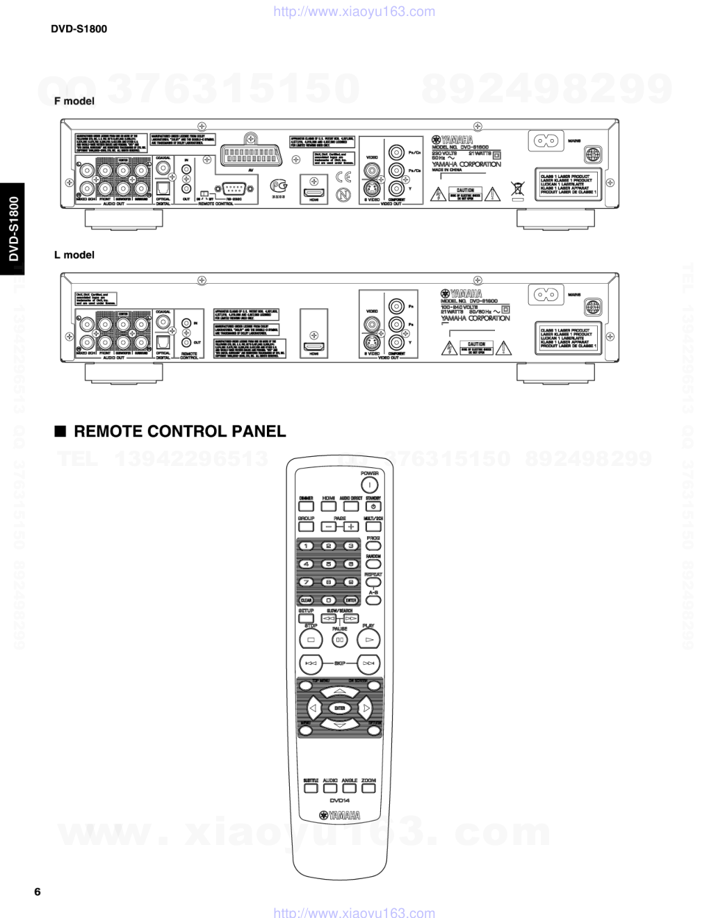
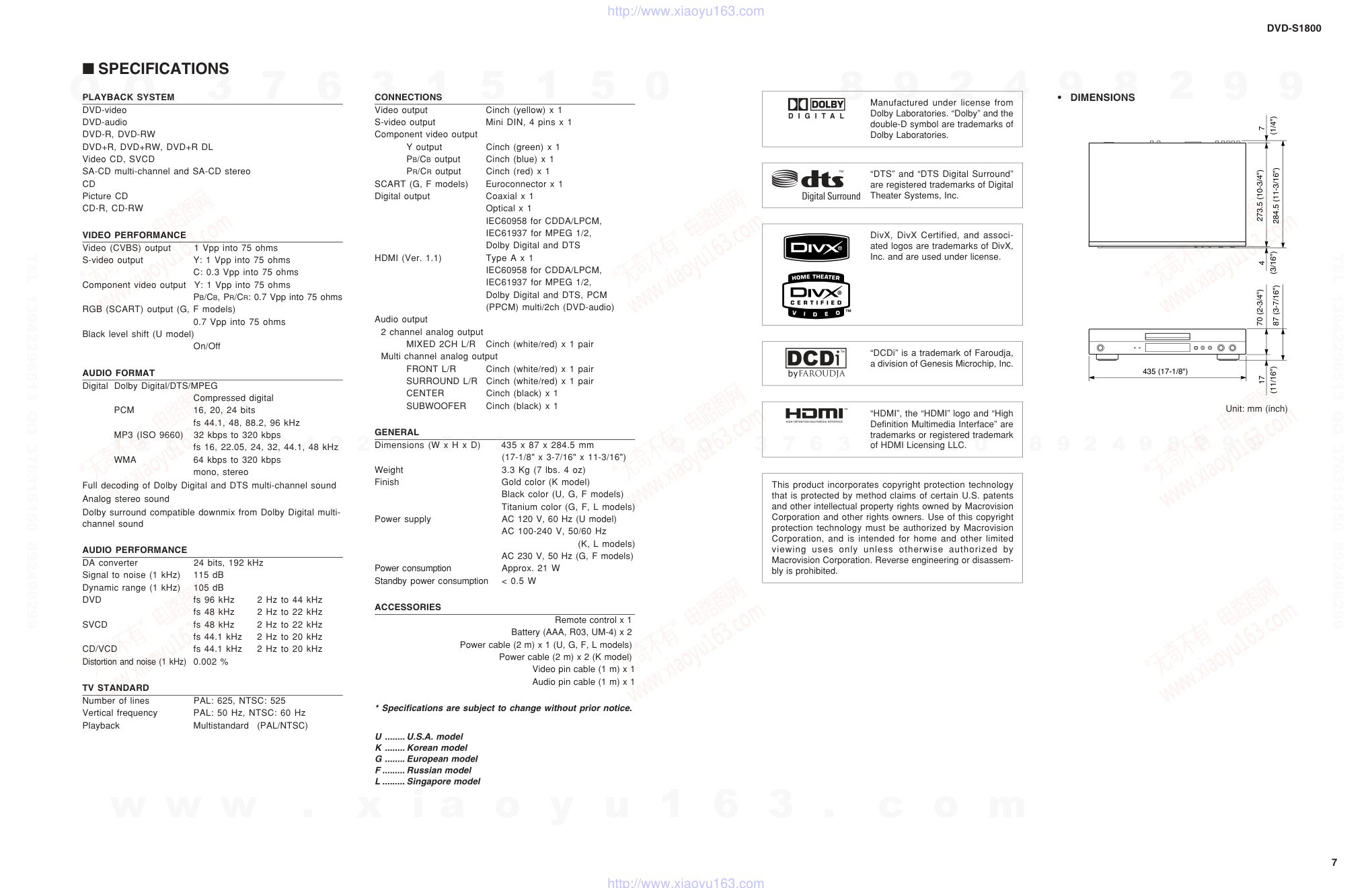
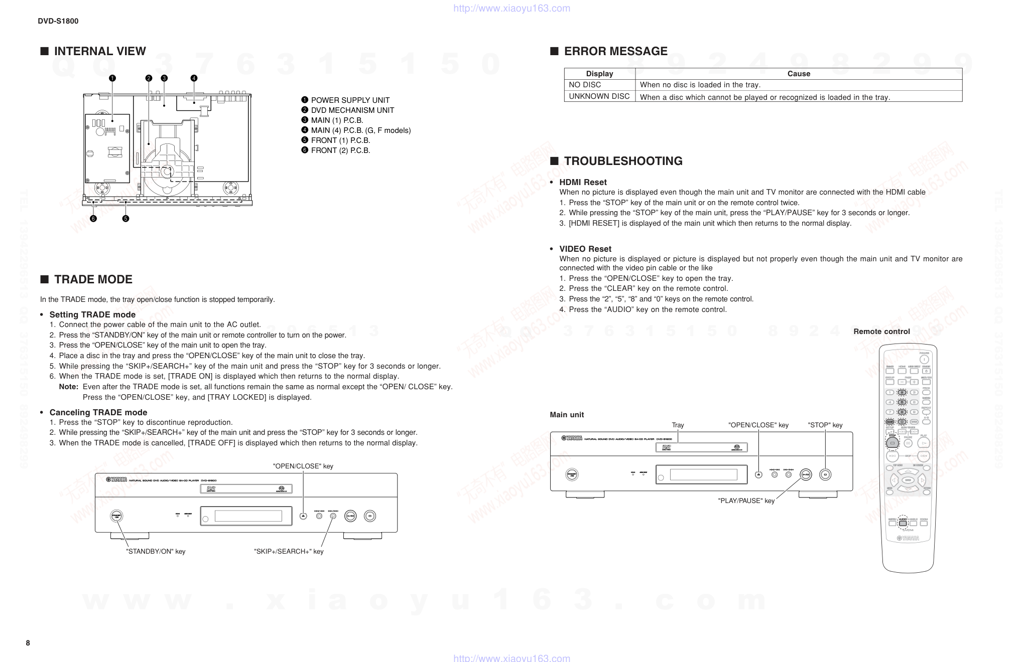
DVD-S1800电路原理图
 "DVD-S1800电路原理图-0")
 "DVD-S1800电路原理图-1")
 "DVD-S1800电路原理图-2")
 "DVD-S1800电路原理图-3")
 "DVD-S1800电路原理图-4")
 "DVD-S1800电路原理图-5")
 "DVD-S1800电路原理图-6")
 "DVD-S1800电路原理图-7")
 "DVD-S1800电路原理图-8")
 "DVD-S1800电路原理图-9")
SERVICE MANUAL 1 0 1 0 7 3 IMPORTANT NOTICE This manual has been provided for the use of authorized YAMAHA Retailers and their service personnel. It has been assumed that basic service procedures inherent to the industry, and more specifically YAMAHA Products, are already known and understood by the users, and have therefore not been restated. WARNING: Failure to follow appropriate service and safety procedures when servicing this product may result in personal injury, destruction of expensive components, and failure of the product to perform as specified. For these reasons, we advise all YAMAHA product owners that any service required should be performed by an authorized YAMAHA Retailer or the appointed service representative. IMPORTANT: The presentation or sale of this manual to any individual or firm does not constitute authorization, certification or recognition of any applicable technical capabilities, or establish a principle-agent relationship of any form. The data provided is believed to be accurate and applicable to the unit(s) indicated on the cover. The research, engineering, and service departments of YAMAHA are continually striving to improve YAMAHA products. Modifications are, therefore, inevitable and specifications are subject to change without notice or obligation to retrofit. Should any discrepancy appear to exist, please contact the distributor's Service Division. WARNING: Static discharges can destroy expensive components. Discharge any static electricity your body may have accumulated by grounding yourself to the ground buss in the unit (heavy gauge black wires connect to this buss). IMPORTANT: Turn the unit OFF during disassembly and part replacement. Recheck all work before you apply power to the unit. DVD AUDIO/VIDEO SA-CD PLAYER DVD-S1800 P.O.Box 1, Hamamatsu, Japan DVD-S1800 2007 All rights reserved. This manual is copyrighted by YAMAHA and may not be copied or redistributed either in print or electronically without permission. '07.09 I CONTENTS TO SERVICE PERSONNEL ...................................... 2–4 PREVENTION OF ELECTROSTATIC DISCHARGE .... 4 LOCALE MANAGEMENT INFORMATION ................... 4 FRONT PANEL .............................................................. 5 REAR PANELS .......................................................... 5–6 REMOTE CONTROL PANEL ........................................ 6 SPECIFICATIONS.......................................................... 7 INTERNAL VIEW ........................................................... 8 TRADE MODE ................................................................ 8 ERROR MESSAGE ........................................................ 8 TROUBLESHOOTING ................................................... 8 DISASSEMBLY PROCEDURES ........................... 10–11 DISPLAY DATA ..................................................... 12–13 IC DATA ................................................................. 14–31 BLOCK DIAGRAM ....................................................... 32 WIRING DIAGRAM ...................................................... 33 PRINTED CIRCUIT BOARDS................................ 34–37 SCHEMATIC DIAGRAMS...................................... 38–44 REPLACEMENT PARTS LIST .............................. 45–47 REMOTE CONTROL.............................................. 48–49 www. xiaoyu163. com QQ 376315150 9 9 2 8 9 4 2 9 8 TEL 13942296513 9 9 2 8 9 4 2 9 8 0 5 1 5 1 3 6 7 3 Q Q TEL 13942296513 QQ 376315150 892498299 TEL 13942296513 QQ 376315150 892498299 http://www.xiaoyu163.com DVD-S1800 2 DVD-S1800 WALL OUTLET EQUIPMENT UNDER TEST AC LEAKAGE TESTER OR EQUIVALENT INSULATING TABLE WARNING: CHEMICAL CONTENT NOTICE! This product contains chemicals known to the State of California to cause cancer, or birth defects or other reproductive harm. DO NOT PLACE SOLDER, ELECTRICAL/ELECTRONIC OR PLASTIC COMPONENTS IN YOUR MOUTH FOR ANY REA- SON WHAT SO EVER! Avoid prolonged, unprotected contact between solder and your skin! When soldering, do not inhale solder fumes or expose eyes to solder/flux vapor! If you come in contact with solder or components located inside the enclosure of this product, wash your hands before handling food. 1. Critical Components Information Components having special characteristics are marked s and must be replaced with parts having specifications equal to those originally installed. 2. Leakage Current Measurement (For 120V Models Only) When service has been completed, it is imperative to verify that all exposed conductive surfaces are prop- erly insulated from supply circuits. G Meter impedance should be equivalent to 1500 ohms shunted by 0.15µF. G Leakage current must not exceed 0.5mA. G Be sure to test for leakage with the AC plug in both polarities. I TO SERVICE PERSONNEL All of the P.C.B.s installed in this unit and solder joints are soldered using the lead free solder. Among some types of lead free solder currently available, it is recommended to use one of the following types for the repair work. • Sn + Ag + Cu (tin + silver + copper) • Sn + Cu (tin + copper) • Sn + Zn + Bi (tin + zinc + bismuth) Caution: As the melting point temperature of the lead free solder is about 30°C to 40°C (50°F to 70°F) higher than that of the lead solder, be sure to use a soldering iron suitable to each solder. About lead free solder WARNING: Laser Safety This product contains a laser beam component. This component may emit invisible, as well as visible radiation, which may cause eye damage. To protect your eyes and skin from laser radiation, the following precautions must be used during servicing of the unit. 1) When testing and/or repairing any component within the product, keep your eyes and skin more than 30 cm away from the laser pick-up unit at all times. Do not stare at the laser beam at any time. 2) Do not attempt to readjust, disassemble or repair the laser pick-up, unless noted elsewhere in this manual. 3) CAUTION : Use of controls, adjustments or performance of procedures other than those specified herein may result in hazardous radiation exposure. www. xiaoyu163. com QQ 376315150 9 9 2 8 9 4 2 9 8 TEL 13942296513 9 9 2 8 9 4 2 9 8 0 5 1 5 1 3 6 7 3 Q Q TEL 13942296513 QQ 376315150 892498299 TEL 13942296513 QQ 376315150 892498299 http://www.xiaoyu163.com DVD-S1800 3 DVD-S1800 Laser Emitting conditions: 1) When the Top Cover is removed, and the STANDBY/ON SW is turned to the "ON" position, the laser component will emit a beam for several seconds to detect if a disc is present. During this time (5-10 sec.) the laser may radiate through the lens of the laser pick-up unit. Do not attempt any servicing during this period! If no disc is detected, the laser will stop emitting the beam. When a disc is loaded, you will not be exposed to any laser emissions. 2) The laser power level can be adjusted with the VR on the pick-up PWB, however, this level has been set by the factory prior to shipping from the factory. Do not adjust this laser level control unless instruction is provided elsewhere in this manual. Adjustment of this control can increase the laser emission level from the device. Laser Diode Properties Type: Semiconductor laser GaAlAs Wave length: 650 nm (DVD) 790 nm (VCD/CD) Output Power: 1.45 mW (DVD) 1.13 mW (VCD/CD) Beam divergence: 60 degrees VARO! : AVATTAESSA JA SUOJALUKITUS OHITETTAESSA OLET ALTTIINA NÄKYMÄTTÖMÄLLE LASER- S Ä T E I L Y L L E . Ä L Ä K A T S O SÄTEESEEN. VARNING! : OSYNLIG LASERSTRÅLNING NÄR DENNA DEL ÄR ÖPPNAD OCH SPÄRREN ÄR URKOPPLAD. BETRAKTA EJ STRÅLEN. www. xiaoyu163. com QQ 376315150 9 9 2 8 9 4 2 9 8 TEL 13942296513 9 9 2 8 9 4 2 9 8 0 5 1 5 1 3 6 7 3 Q Q TEL 13942296513 QQ 376315150 892498299 TEL 13942296513 QQ 376315150 892498299 http://www.xiaoyu163.com DVD-S1800 4 DVD-S1800 I PREVENTION OF ELECTROSTATIC DISCHARGE This product incorporates copyright protec- tion technology that is protected by method claims of certain U.S. patents and other intellectual property rights owned by Macrovision Corporation and other rights owners. Use of this copyright protection technology must be authorized by Macrovision Corporation, and is intended for home and other limited viewing uses only unless oth- erwise authorized by Macrovision Corpora- tion. Reverse engineering or disassembly is prohibited. The laser diode in the DVD mechanism may be damaged due to static electricity from clothes or the human body. Use caution to prevent electrostatic damage when servicing or handling the DVD-mechanism. 1. Grounding for electrostatic damage prevention Some devices, such as the DVD player, use an optical pickup (laser diode) that will be damaged by static electricity in the working environment. Only attempt service after ensuring that all grounding procedures have been completed. 1. Worktable grounding Put a grounded conductive material (sheet) or iron sheet on the area where the optical pickup is placed. 2. Human body grounding Use an anti-static wrist strap to discharge the static electricity from your body. 2. Handling Precautions for DVD mechanism 1. Handle the DVD mechanism gently, as it is an extremely high-precision assembly. 2. The flexible cable lines may break if an excessive force is applied to it. Use caution when handling the cable. 3. The semi-fixed resistor for laser power adjustment should not be adjusted. Do not turn the resistor. I LOCALE MANAGEMENT INFORMATION Locale Management Information : This DVD player is designed and manufactured to respond to the Locale Management Information that is recorded on a DVD disc. If the Locale number described on the DVD disc does not correspond to the Locale number of this DVD player, this DVD player cannot play this disc. Warning for power supply The primary side of the power supply carries live mains voltage when the player is connected to the mains even when the player is switched off ! This primary area is not shielded so it is possible to touch copper tracks and/or components when servicing the player. Service personnel have to take precautions to prevent touching this area or components in this area. Note: The screws on the DVD mechanism may never be touched, removed or re-adjusted. Handle the DVD mechanism with care when the unit has to be exchanged! The DVD mechanism is very sensitive for dropping or giving shocks. 1M-ohms Conductive material (sheet) or steel sheet Anti-static wrist strap 1 4 2 2 2 5 5 5 4 3 6 www. xiaoyu163. com QQ 376315150 9 9 2 8 9 4 2 9 8 TEL 13942296513 9 9 2 8 9 4 2 9 8 0 5 1 5 1 3 6 7 3 Q Q TEL 13942296513 QQ 376315150 892498299 TEL 13942296513 QQ 376315150 892498299 http://www.xiaoyu163.com www. xiaoyu163. com QQ 376315150 9 9 2 8 9 4 2 9 8 TEL 13942296513 9 9 2 8 9 4 2 9 8 0 5 1 5 1 3 6 7 3 Q Q TEL 13942296513 QQ 376315150 892498299 TEL 13942296513 QQ 376315150 892498299 http://www.xiaoyu163.com www. xiaoyu163. com QQ 376315150 9 9 2 8 9 4 2 9 8 TEL 13942296513 9 9 2 8 9 4 2 9 8 0 5 1 5 1 3 6 7 3 Q Q TEL 13942296513 QQ 376315150 892498299 TEL 13942296513 QQ 376315150 892498299 http://www.xiaoyu163.com DVD-S1800 7 “HDMI”, the “HDMI” logo and “High Definition Multimedia Interface” are trademarks or registered trademark of HDMI Licensing LLC. I SPECIFICATIONS Manufactured under license from Dolby Laboratories. “Dolby” and the double-D symbol are trademarks of Dolby Laboratories. • DIMENSIONS Unit: mm (inch) PLAYBACK SYSTEM DVD-video DVD-audio DVD-R, DVD-RW DVD+R, DVD+RW, DVD+R DL Video CD, SVCD SA-CD multi-channel and SA-CD stereo CD Picture CD CD-R, CD-RW VIDEO PERFORMANCE Video (CVBS) output 1 Vpp into 75 ohms S-video output Y: 1 Vpp into 75 ohms C: 0.3 Vpp into 75 ohms Component video output Y: 1 Vpp into 75 ohms PB/CB, PR/CR: 0.7 Vpp into 75 ohms RGB (SCART) output (G, F models) 0.7 Vpp into 75 ohms Black level shift (U model) On/Off AUDIO FORMAT Digital Dolby Digital/DTS/MPEG Compressed digital PCM 16, 20, 24 bits fs 44.1, 48, 88.2, 96 kHz MP3 (ISO 9660) 32 kbps to 320 kbps fs 16, 22.05, 24, 32, 44.1, 48 kHz WMA 64 kbps to 320 kbps mono, stereo Full decoding of Dolby Digital and DTS multi-channel sound Analog stereo sound Dolby surround compatible downmix from Dolby Digital multi- channel sound AUDIO PERFORMANCE DA converter 24 bits, 192 kHz Signal to noise (1 kHz) 115 dB Dynamic range (1 kHz) 105 dB DVD fs 96 kHz 2 Hz to 44 kHz fs 48 kHz 2 Hz to 22 kHz SVCD fs 48 kHz 2 Hz to 22 kHz fs 44.1 kHz 2 Hz to 20 kHz CD/VCD fs 44.1 kHz 2 Hz to 20 kHz Distortion and noise (1 kHz) 0.002 % TV STANDARD Number of lines PAL: 625, NTSC: 525 Vertical frequency PAL: 50 Hz, NTSC: 60 Hz Playback Multistandard (PAL/NTSC) CONNECTIONS Video output Cinch (yellow) x 1 S-video output Mini DIN, 4 pins x 1 Component video output Y output Cinch (green) x 1 PB/CB output Cinch (blue) x 1 PR/CR output Cinch (red) x 1 SCART (G, F models) Euroconnector x 1 Digital output Coaxial x 1 Optical x 1 IEC60958 for CDDA/LPCM, IEC61937 for MPEG 1/2, Dolby Digital and DTS HDMI (Ver. 1.1) Type A x 1 IEC60958 for CDDA/LPCM, IEC61937 for MPEG 1/2, Dolby Digital and DTS, PCM (PPCM) multi/2ch (DVD-audio) Audio output 2 channel analog output MIXED 2CH L/R Cinch (white/red) x 1 pair Multi channel analog output FRONT L/R Cinch (white/red) x 1 pair SURROUND L/R Cinch (white/red) x 1 pair CENTER Cinch (black) x 1 SUBWOOFER Cinch (black) x 1 GENERAL Dimensions (W x H x D) 435 x 87 x 284.5 mm (17-1/8" x 3-7/16" x 11-3/16") Weight 3.3 Kg (7 lbs. 4 oz) Finish Gold color (K model) Black color (U, G, F models) Titanium color (G, F, L models) Power supply AC 120 V, 60 Hz (U model) AC 100-240 V, 50/60 Hz (K, L models) AC 230 V, 50 Hz (G, F models) Power consumption Approx. 21 W Standby power consumption < 0.5 W ACCESSORIES Remote control x 1 Battery (AAA, R03, UM-4) x 2 Power cable (2 m) x 1 (U, G, F, L models) Power cable (2 m) x 2 (K model) Video pin cable (1 m) x 1 Audio pin cable (1 m) x 1 * Specifications are subject to change without prior notice. This product incorporates copyright protection technology that is protected by method claims of certain U.S. patents and other intellectual property rights owned by Macrovision Corporation and other rights owners. Use of this copyright protection technology must be authorized by Macrovision Corporation, and is intended for home and other limited viewing uses only unless otherwise authorized by Macrovision Corporation. Reverse engineering or disassem- bly is prohibited. 435 (17-1/8") 87 (3-7/16") 70 (2-3/4") 273.5 (10-3/4") 17 (11/16") 4 (3/16") 284.5 (11-3/16") 7 (1/4") U ........ U.S.A. model K ........ Korean model G ........ European model F ......... Russian model L ......... Singapore model “DTS” and “DTS Digital Surround” are registered trademarks of Digital Theater Systems, Inc. DivX, DivX Certified, and associ- ated logos are trademarks of DivX, Inc. and are used under license. “DCDi” is a trademark of Faroudja, a division of Genesis Microchip, Inc. w w w . x i a o y u 1 6 3 . c o m Q Q 3 7 6 3 1 5 1 5 0 9 9 2 8 9 4 2 9 8 T E L 1 3 9 4 2 2 9 6 5 1 3 9 9 2 8 9 4 2 9 8 0 5 1 5 1 3 6 7 3 Q Q TEL 13942296513 QQ 376315150 892498299 TEL 13942296513 QQ 376315150 892498299 http://www.xiaoyu163.com DVD-S1800 8 NO DISC UNKNOWN DISC When no disc is loaded in the tray. When a disc which cannot be played or recognized is loaded in the tray. I INTERNAL VIEW 1 2 3 4 5 6 1 2 3 4 5 6 POWER SUPPLY UNIT DVD MECHANISM UNIT MAIN (1) P.C.B. MAIN (4) P.C.B. (G, F models) FRONT (1) P.C.B. FRONT (2) P.C.B. � I ERROR MESSAGE I TRADE MODE In the TRADE mode, the tray open/close function is stopped temporarily. • Setting TRADE mode 1. Connect the power cable of the main unit to the AC outlet. 2. Press the “STANDBY/ON” key of the main unit or remote controller to turn on the power. 3. Press the “OPEN/CLOSE” key of the main unit to open the tray. 4. Place a disc in the tray and press the “OPEN/CLOSE” key of the main unit to close the tray. 5. While pressing the “SKIP+/SEARCH+” key of the main unit and press the “STOP” key for 3 seconds or longer. 6. When the TRADE mode is set, [TRADE ON] is displayed which then returns to the normal display. Note: Even after the TRADE mode is set, all functions remain the same as normal except the “OPEN/ CLOSE” key. Press the “OPEN/CLOSE” key, and [TRAY LOCKED] is displayed. • Canceling TRADE mode 1. Press the “STOP” key to discontinue reproduction. 2. While pressing the “SKIP+/SEARCH+” key of the main unit and press the “STOP” key for 3 seconds or longer. 3. When the TRADE mode is cancelled, [TRADE OFF] is displayed which then returns to the normal display. Display Cause I TROUBLESHOOTING • HDMI Reset When no picture is displayed even though the main unit and TV monitor are connected with the HDMI cable 1. Press the “STOP” key of the main unit or on the remote control twice. 2. While pressing the “STOP” key of the main unit, press the “PLAY/PAUSE” key for 3 seconds or longer. 3. [HDMI RESET] is displayed of the main unit which then returns to the normal display. • VIDEO Reset When no picture is displayed or picture is displayed but not properly even though the main unit and TV monitor are connected with the video pin cable or the like 1. Press the “OPEN/CLOSE” key to open the tray. 2. Press the “CLEAR” key on the remote control. 3. Press the “2”, “5”, “8” and “0” keys on the remote control. 4. Press the “AUDIO” key on the remote control. "STOP" key "PLAY/PAUSE" key Tray "OPEN/CLOSE" key Main unit Remote control "OPEN/CLOSE" key "STANDBY/ON" key "SKIP+/SEARCH+" key w w w . x i a o y u 1 6 3 . c o m Q Q 3 7 6 3 1 5 1 5 0 9 9 2 8 9 4 2 9 8 T E L 1 3 9 4 2 2 9 6 5 1 3 9 9 2 8 9 4 2 9 8 0 5 1 5 1 3 6 7 3 Q Q TEL 13942296513 QQ 376315150 892498299 TEL 13942296513 QQ 376315150 892498299 http://www.xiaoyu163.com 9 DVD-S1800 DVD-S1800 MEMO MEMO www. xiaoyu163. com QQ 376315150 9 9 2 8 9 4 2 9 8 TEL 13942296513 9 9 2 8 9 4 2 9 8 0 5 1 5 1 3 6 7 3 Q Q TEL 13942296513 QQ 376315150 892498299 TEL 13942296513 QQ 376315150 892498299 http://www.xiaoyu163.com 10 DVD-S1800 DVD-S1800 Fig. 1 I DISASSEMBLY PROCEDURES (Remove parts in disassembly order as numbered.) Disconnect the power cable from the AC outlet. 1. Removal of Top Cabinet a. Remove 6 screws (1). (Fig. 1) b. Lift up the rear side of the top cover, then remove rear- ward. (Fig. 1) 1 Top cover Front panel ass'y Front panel ass'y Front panel ass'y Tray lid Hook Hook Hook Hook DVD mechanism unit 1 1 1 2 3 4 4 Front Front DVD mechanism unit 2. Removal of DVD Mechanism Unit a. Eject the tray. (See “How to manually eject the tray”.) b. Remove the tray lid upward and close the tray. (Fig. 1) c. Remove 2 screws (2). (Fig. 1) d. Turn the traverse gear in the arrow direction until the P.C.B. of the DVD mechanism unit is seen. (Fig. 2) e. Solder the lands in the P.C.B. of the DVD mechanism unit with the anti-static soldering iron. (Fig. 2) Note • After you have finished repairing , connect the flexible flat cable to CN11 in advance and then re- move the solder from the short-circuit location with the anti-static soldering iron. www. xiaoyu163. com QQ 376315150 9 9 2 8 9 4 2 9 8 TEL 13942296513 9 9 2 8 9 4 2 9 8 0 5 1 5 1 3 6 7 3 Q Q TEL 13942296513 QQ 376315150 892498299 TEL 13942296513 QQ 376315150 892498299 http://www.xiaoyu163.com 11 DVD-S1800 DVD-S1800 CN12 CN11 CN13 CX41 MAIN (1) P.C.B. DVD mechanism unit Solder P.C.B. DVD mechanism unit Traverse gear Unlocked Locked Flexible flat cable CN11 CN11 3. Removal of Front Panel Ass’y a. Remove 4 screws (3). (Fig. 1) b. Remove 2 screws (4). (Fig. 1) c. Remove CX41. (Fig. 2) d. Remove 2 hooks and then remove the front panel ass’y forward. (Fig. 1) Fig. 2 e. Remove CN11, CN12 and CN13. (Fig. 2) f. Lift up the rear side of the DVD mechanism unit, then remove 2 hooks and remove rearward. (Fig. 1) Tray Loading gear Bottom side Tray Flatblade screwdriver • How to manually eject the tray a. Turn the loading gear in the direction indicated with a flatblade screwdriver until the tray is ejected. b. Gently pull the tray out. www. xiaoyu163. com QQ 376315150 9 9 2 8 9 4 2 9 8 TEL 13942296513 9 9 2 8 9 4 2 9 8 0 5 1 5 1 3 6 7 3 Q Q TEL 13942296513 QQ 376315150 892498299 TEL 13942296513 QQ 376315150 892498299 http://www.xiaoyu163.com 12 DVD-S1800 DVD-S1800 I DISPLAY DATA G F401 : HCA14SM16 (FRONT P.C.B.) G PIN CONNECTION G GRID ASSIGNMENT Pin No. Connection 25 NX Note : 1) F1, F2 ..... Filament pin 2) NP ..... No pin 3) NC ..... No connection 4) NX ..... No extended pin 3G 2G 4G 5G 6G 7G 8G 9G 1G (2G-14G) 10G 11G 1 2 3 4 5 6 7 8 9 10 11 12 13 14 15 16 17 18 19 20 21 22 23 24 25 26 27 28 29 30 31 32 33 34 35 12G 13G 14G j 1 PATTERN AREA 24 NX 23 NX 22 NX 21 NX 20 NX 19 NX 18 NX 17 NX 16 1G 15 NC 14 GR1 13 VDD 12 DIN 11 CLKB 10 CSB 9 RSTB 8 OSCO 7 OSCI 6 VEE 5 GND 4 NP 3 NP 2 F1 1 F1 Pin No. Connection 50 F2 49 F2 48 NP 47 NP 46 NX 45 NX 44 NX 43 NX NX NX NX NX NX NX NX NX NX NX NX NX NX NX NX NX NX 42 41 40 39 38 37 36 35 34 33 32 31 30 29 28 27 26 www. xiaoyu163. com QQ 376315150 9 9 2 8 9 4 2 9 8 TEL 13942296513 9 9 2 8 9 4 2 9 8 0 5 1 5 1 3 6 7 3 Q Q TEL 13942296513 QQ 376315150 892498299 TEL 13942296513 QQ 376315150 892498299 http://www.xiaoyu163.com 13 DVD-S1800 DVD-S1800 SG1 SG2 SG3 SG4 SG5 SG6 SG7 SG8 SG9 SG10 SG11 SG12 SG13 SG14 SG15 SG16 SG17 SG18 SG19 SG20 SG21 SG22 SG23 SG24 SG25 SG26 SG27 SG28 SG29 SG30 SG31 SG32 SG33 SG34 SG35 GR14 14G 1 2 3 4 5 6 7 8 9 10 11 12 13 14 15 16 17 18 19 20 21 22 23 24 25 26 27 28 29 30 31 32 33 34 35 GR13 13G 1 2 3 4 5 6 7 8 9 10 11 12 13 14 15 16 17 18 19 20 21 22 23 24 25 26 27 28 29 30 31 32 33 34 35 GR12 12G 1 2 3 4 5 6 7 8 9 10 11 12 13 14 15 16 17 18 19 20 21 22 23 24 25 26 27 28 29 30 31 32 33 34 35 GR11 11G 1 2 3 4 5 6 7 8 9 10 11 12 13 14 15 16 17 18 19 20 21 22 23 24 25 26 27 28 29 30 31 32 33 34 35 GR10 10G 1 2 3 4 5 6 7 8 9 10 11 12 13 14 15 16 17 18 19 20 21 22 23 24 25 26 27 28 29 30 31 32 33 34 35 GR9 9G 1 2 3 4 5 6 7 8 9 10 11 12 13 14 15 16 17 18 19 20 21 22 23 24 25 26 27 28 29 30 31 32 33 34 35 GR8 8G 1 2 3 4 5 6 7 8 9 10 11 12 13 14 15 16 17 18 19 20 21 22 23 24 25 26 27 28 29 30 31 32 33 34 35 GR7 7G 1 2 3 4 5 6 7 8 9 10 11 12 13 14 15 16 17 18 19 20 21 22 23 24 25 26 27 28 29 30 31 32 33 34 35 GR6 6G 1 2 3 4 5 6 7 8 9 10 11 12 13 14 15 16 17 18 19 20 21 22 23 24 25 26 27 28 29 30 31 32 33 34 35 GR5 5G 1 2 3 4 5 6 7 8 9 10 11 12 13 14 15 16 17 18 19 20 21 22 23 24 25 26 27 28 29 30 31 32 33 34 35 GR4 4G 1 2 3 4 5 6 7 8 9 10 11 12 13 14 15 16 17 18 19 20 21 22 23 24 25 26 27 28 29 30 31 32 33 34 35 GR3 3G 1 2 3 4 5 6 7 8 9 10 11 12 13 14 15 16 17 18 19 20 21 22 23 24 25 26 27 28 29 30 31 32 33 34 35 GR2 2G 1 2 3 4 5 6 7 8 9 10 11 12 13 14 15 16 17 18 19 20 21 22 23 24 25 26 27 28 29 30 31 32 33 34 35 GR1 1G G ANODE CONNECTION www. xiaoyu163. com QQ 376315150 9 9 2 8 9 4 2 9 8 TEL 13942296513 9 9 2 8 9 4 2 9 8 0 5 1 5 1 3 6 7 3 Q Q TEL 13942296513 QQ 376315150 892498299 TEL 13942296513 QQ 376315150 892498299 http://www.xiaoyu163.com 14 DVD-S1800 DVD-S1800 I IC DATA TRAY IR-RC Receiver Front Panel Concentrator SPI/I2C/GPIO/DDC MICROPROCESSOR SERVO v v v v v v v v AFE ADP DSP MCU VPU PLL 27 MHz 8/16 Mbits NOR Flash RESET 32/64/128 Mbits SDRAM IC11 Vaddis ZR36778 SPINDLE SLED OPU Disc loader RF amp Servo amp S/PDIF Audio ADC Stereo Mics 2 to 8 Speakers TV Monitor DAC IC11: ZR36778 (MAIN P.C.B.) MPEG decoder www. xiaoyu163. com QQ 376315150 9 9 2 8 9 4 2 9 8 TEL 13942296513 9 9 2 8 9 4 2 9 8 0 5 1 5 1 3 6 7 3 Q Q TEL 13942296513 QQ 376315150 892498299 TEL 13942296513 QQ 376315150 892498299 http://www.xiaoyu163.com 15 DVD-S1800 DVD-S1800 1 2 3 4,5 6 7 8 9 10 11 12 13 14 15 16 17 18-19 20 21 22 23 24 25 26 27 28 29 30 31 32 33 34 35 36 37 38 SSCRXD GPCI/O[17] PM[15] MEMCS[1]# GPCI/O[18] VDDP MEMAD [15,16] SYSIND[1,0] MEMAD[14] GCLKSEL MEMAD[13] FCUIF[29] MEMAD[12] PLLCFGA MEMDA[15] FCUIF[28] MEMAD[11] PLLCFGP MEMDA[7] FCUIF[9] GNDP MEMAD[10] FCUIF[20] MEMDA[14] FCUIF[27] MEMAD[9] FCUIF[19] MEMDA[6] FCUIF[8] MEMAD[8] FCUIF[18] MEMDA[13,5] FCUIF[26,7] MEMAD[20] MEMCS[2]# GPCI/O[19] VDDP MEMDA[12] FCUIF[25] MEMWR# FCUIF[0] MEMDA[4] FCUIF[6] VDDC MEMDA[11] FCUIF[24] MEMDA[3] FCUIF[5] MEMAD[19] PLLSEL GNDC MEMDA[10] FCUIF[23] MEMAD[18] GNDP MEMDA[2] FCUIF[4] MEMAD[17] MEMDA[9] FCUIF[22] MEMAD[7] FCUIF[17] MEMDA[1] FCUIF[3] MEMAD[6] I I/O O O I/O S O I O I O O O I I/O I/O O I I/O I/O S O O I/O I/O O O I/O I/O O O I/O I/O O O I/O S I/O I/O O O I/O O S I/O I/O I/O I/O O I S I/O I/O O S I/O I/O O I/O I/O O O I/O I/O O SSC data input General purpose I/O, monitored/controlled by the microprocessor or DSP or FCU SW Probe mux data output PNVM/SRAM chip select (active low) output General purpose I/O, monitored/controlled by the microprocessor or DSP SW 3.3 V digital periphery power supply PNVM/SRAM address bus outputs General purpose system configuration indication input / Level sampled during RESET PNVM/SRAM address bus output GCLKPOUT or GCLKA function selection / Level sampled during RESET PNVM/SRAM address bus output Flash card interface unit output signal PNVM/SRAM address bus output Audio PLL configuration input / Level sampled during RESET / In normal operation the pin must be low during RESET PNVM/SRAM bi-directional data bus Flash card interface unit I/O signal PNVM/SRAM address bus output Process PLL configuration input / Level sampled during RESET / In normal operation the pin must be low during RESET PNVM/SRAM bi-directional data bus Flash card interface unit I/O signals Digital periphery ground of 3.3 V supply PNVM/SRAM address bus output Flash card interface unit output signal PNVM/SRAM bi-directional data bus Flash card interface unit I/O signal PNVM/SRAM address bus outputs Flash card interface unit output signal PNVM/SRAM bi-directional data bus Flash card interface unit I/O signals PNVM/SRAM address bus outputs Flash card interface unit output signal PNVM/SRAM bi-directional data bus Flash card interface unit I/O signals PNVM/SRAM address bus outputs PNVM/SRAM chip select (active low) output General purpose I/O, monitored/controlled by the microprocessor or DSP SW 3.3 V digital periphery power supply PNVM/SRAM bi-directional data bus Flash card interface unit I/O signal PNVM/SRAM write enable (active low) output Flash card interface unit output signal PNVM/SRAM bi-directional data bus Flash card interface unit output signal 1.8 V digital core power supply PNVM/SRAM bi-directional data bus Flash card interface unit I/O signal PNVM/SRAM bi-directional data bus Flash card interface unit I/O signals PNVM/SRAM address bus outputs PLL frequency selection -108 MHz (low) or 135 MHz (high) / Level sampled during RESET Digital core ground of 1.8 V supply PNVM/SRAM bi-directional data bus Flash card interface unit I/O signal PNVM/SRAM address bus output Digital periphery ground of 3.3 V supply PNVM/SRAM bi-directional data bus Flash card interface unit I/O signals PNVM/SRAM address bus output PNVM/SRAM bi-directional data bus Flash card interface unit I/O signal PNVM/SRAM address bus outputs Flash card interface unit output signal PNVM/SRAM bi-directional data bus Flash card interface unit I/O signals PNVM/SRAM address bus outputs Pin Functions Direction Description No. www. xiaoyu163. com QQ 376315150 9 9 2 8 9 4 2 9 8 TEL 13942296513 9 9 2 8 9 4 2 9 8 0 5 1 5 1 3 6 7 3 Q Q TEL 13942296513 QQ 376315150 892498299 TEL 13942296513 QQ 376315150 892498299 http://www.xiaoyu163.com 16 DVD-S1800 DVD-S1800 39 40 41 42 43 44 45-46 47 48 49 50 51 52 53-57 58 59-61 62 63 64 65 66 67 68 69 70 71 72 73 74 75 76 77 78 79 80 81 82 83 84-86 87 88-90 91 FCUIF[16] MEMDA[8] FCUIF[21] MEMAD[5] FCUIF[15] VDDP MEMDA[0] FCUIF[2] MEMAD[4] FCUIF[14] MEMRD# FCUIF[1] MEMAD[3, 2] FCUIF[13, 12] MEMCS[0]# MEMAD[1] FCUIF[11] BOOTSEL[2] MEMAD[0] FCUIF[10] BOOTSEL[1] GNDP VDD-IP VDDP RAMADD [4, 3, 5, 2, 6] VDDP RAMADD [1, 7, 0] GNDP RAMADD[8] VDDC RAMADD[10] GNDC RAMADD[9] VDDP RAMADD[11] RAMCS[0]# RAMBA[1] RAMBA[0] GNDP RAMCS[1]# RAMRAS# RAMCAS# VDDP RAMWE# RAMDQM GNDPCLK PCLK VDDPCLK RAMDAT[8] GNDP RAMDAT [7, 9, 6] VDDP RAMDAT [10, 5, 11] GNDP O I/O I/O O O S I/O O I/O O O I/O O O O O O I O O I S S S O S O S O S O S O S O O O O S O O O S O O S O S I/O S I/O S I/O S Flash card interface unit output signal PNVM/SRAM bi-directional data bus Flash card interface unit I/O signal PNVM/SRAM address bus outputs Flash card interface unit output signal 3.3 V digital periphery power supply PNVM/SRAM bi-directional data bus Flash card interface unit output signal PNVM/SRAM address bus outputs Flash card interface unit output signal PNVM/SRAM read enable (active low) output Flash card interface unit I/O signal PNVM/SRAM address bus outputs Flash card interface unit output signal PNVM/SRAM chip select (active low) output PNVM/SRAM address bus outputs Flash card interface unit output signals Microprocessor SW boot (and execute) source selection: (high, high) - For production testing; (high, low) - Flash+SRAM (for debug monitor); (low, high) - First debug UART (low, low) - Flash (low) or Level sampled during RESET PNVM/SRAM address bus outputs Flash card interface unit output signals Microprocessor SW boot (and execute) source selection: (high, high) - For production testing; (high, low) - Flash+SRAM (for debug monitor); (low, high) - First debug UART (low, low) - Flash (low) or Level sampled during RESET Digital periphery ground of 3.3 V supply 3.3 V periphery reference voltage 3.3 V digital periphery power supply SDRAM address bus output 3.3 V digital periphery power supply SDRAM address bus output Digital periphery ground of 3.3 V supply SDRAM address bus output 1.8 V digital core power supply SDRAM address bus output Digital core ground of 1.8 V supply SDRAM address bus output 3.3 V digital periphery power supply SDRAM address bus output SDRAM chip select (active low) SDRAM bank select output SDRAM bank select output Digital periphery ground of 3.3 V supply SDRAM chip select (active low) output SDRAM row select (active low) output SDRAM column select (active low) output 3.3 V digital periphery power supply SDRAM write enable (active low) output SDRAM data masking (active high) output Digital ground of filtered 3.3 V supply for PCLK SDRAM clock output (same as internal processing clock) 3.3 V filtered digital power supply for PCLK SDRAM bi-directional data bus Digital periphery ground of 3.3 V supply SDRAM bi-directional data bus 3.3 V digital periphery power supply SDRAM bi-directional data bus Digital periphery ground of 3.3 V supply Pin Functions Direction Description No. www. xiaoyu163. com QQ 376315150 9 9 2 8 9 4 2 9 8 TEL 13942296513 9 9 2 8 9 4 2 9 8 0 5 1 5 1 3 6 7 3 Q Q TEL 13942296513 QQ 376315150 892498299 TEL 13942296513 QQ 376315150 892498299 http://www.xiaoyu163.com 17 DVD-S1800 DVD-S1800 92 93 94 95 96 97 98-100 101 102-104 105 106 107 108 109 110 111 112 113 114 115 116 117 118 119 120 121 122 123 124 125 126 RAMDAT[4] VDDC RAMDAT[12] GNDC RAMDAT[3] VDDP RAMDAT [13, 2, 14] GNDP RAMDAT [1, 15, 0] VDDP GPCI/O[20] CPUNMI SDATA[0] PM[0] GNDP ICGPCI/O[0] AOUT[3] SDATA[1] PM[1] IDGPCI/O[0] RAMCKE SDATA[2] PM[2] S/PDIFOUT SDATA[3] PM[3] AOUT[2] GPCI/O[21] SDATA[4] PM[4] AOUT[1] GPCI/O[22] PM[5] AOUT[0] SDATA[6] PM[6] GPAI/O AOUT[3] IDGPCI/O[0] PM[7] ALRCLK ABCLK GNDP-A2 AMCLK VDDP-A2 AIN GPCI/O[23] PM[8] GNDC VSYNC# HDFI GPI/O[24] DACTEST[9] PM[9] VDDC HSYNC# HDHS GPCI/O[25] GNDP VCLKx2 I/O S I/O S I/O S I/O S I/O S I/O I I O S I/O O I O I/O O I O O I O O I/O I O O I/O O O I O I/O O I/O O O O S I/O S I I/O O S O I I/O I O S O I I/O S O SDRAM bi-directional data bus 1.8 V digital core power supply SDRAM bi-directional data bus Digital core ground of 1.8 V supply SDRAM bi-directional data bus 3.3 V digital periphery power supply SDRAM bi-directional data bus Digital periphery ground of 3.3 V supply SDRAM bi-directional data bus 3.3 V digital periphery power supply General purpose I/O, monitored/controlled by the microprocessor or DSP SW Microprocessor non-maskable interrupt input SERVO channel sample data input for AFE by-pass Probe mux data output Digital periphery ground of 3.3 V supply General purpose I/O, monitored/controlled by the microprocessor or DSP SW When input, the pin can be used as general purpose external interrupt to the microprocessor Serial output of digital stereo audio SERVO channel sample data input for AFE by-pass Probe mux data output General purpose I/O, monitored/controlled by the microprocessor or DSP SW When input, the pin can be used as general purpose external interrupt to the DSP Clock enable signal to the SDRAM (for power down) SERVO channel sample data input for AFE by-pass Probe mux data output S/PDIF transmitter output for digital coded or reconstructed audio data SERVO channel sample data input for AFE by-pass Probe mux data output Serial outputs of digital stereo audio General purpose I/O, monitored/controlled by the microprocessor or DSP SW SERVO channel sample data inputs for AFE by-pass Probe mux data outputs Serial output of digital stereo audio General purpose I/O, monitored/controlled by the microprocessor or DSP SW Probe mux data outputs Serial output of digital stereo audio SERVO channel sample data input for AFE by-pass Probe mux data outputs General purpose I/O, monitored/controlled by the ADP SW Serial output of digital stereo audio General purpose I/O, monitored/controlled by the microprocessor or DSP SW When input, the pin can be used as general purpose external interrupt to the DSP Probe mux data output Digital audio left/right select output for the audio port / Square wave, at the sampling frequency / Programmable polarity Digital audio bit-clock output / Data on AOUT and AIN is output or latched, respectively, with the rising or falling (programmable) edge of this clock Digital ground filtered 3.3 V supply for AMCLK Audio master clock I/O / 128, 192, 256 or 384 times the sampling frequency (programmable) 3.3 V filtered digital power supply for AMCLK Serial input of digital stereo audio General purpose I/O, monitored/controlled by the microprocessor or DSP SW Probe mux data output Digital core ground of 1.8 V supply SD digital video vertical sync output signal HD digital video field index input signal General purpose I/O, monitored/controlled by the microprocessor or DSP SW DACs test input Probe mux data output 1.8 V digital core power supply SD digital video horizontal sync output signal HD digital video horizontal sync input signal General purpose I/O, monitored/controlled by the microprocessor or DSP SW Digital periphery ground of 3.3 V supply Digital video clock output / 27,000 (for SD interlaced), 54,000 (SD progressive) or 135,000 (for HD) MHz Pin Functions Direction Description No. www. xiaoyu163. com QQ 376315150 9 9 2 8 9 4 2 9 8 TEL 13942296513 9 9 2 8 9 4 2 9 8 0 5 1 5 1 3 6 7 3 Q Q TEL 13942296513 QQ 376315150 892498299 TEL 13942296513 QQ 376315150 892498299 http://www.xiaoyu163.com 18 DVD-S1800 DVD-S1800 127 128 129 130 131 132 133 134 135 136 137 138 139 140 141 142 143 144 145 146 147 148 149 150 151 152 153 154 155 156 157 158 159 COSYNC ICGPCI/O[1] VDDP VID[7] GPCI/O[26] VID[6] ICGPCI/O[2] VID[5] IDGPCI[1] GNDP VID[4] GPCI/O[27] VID[3] GPCI/O[28] SERVOCLK VID[2] GPCI/O[29] SSEL[0] VDDP VID[1] GPCI/O[30] SSEL[1] VID[0] ICGPCI/O[3] GNDP GNDA RESET# VDDA XO GCLKP GCLKA GPCI/O[31] GCLKPOUT VDDP ICGPCI/O[4] S/PDIFIN[0] GPCI/O[33] ICGPCI/O[5] S/PDIFIN[1] GPCI/O[34] IDGPCI/O[3] FCUIF[33] GNDP DUPRD0 GPCI/O[35] DUPTD0 GPCI/O[36] VDD-IP DUPRD1 GPCI/O[37] DUPTD1 GPCI/O[38] GNDDACD CVBS/G/Y (DAC A) CVBS/C (DAC D) O I/O S O I/O O I/O O I/O S O I/O O I/O O O I/O O S O I/O O O I/O S S ID S AO ID ID I/O O S I/O I I/O I/O I I/O I/O I S I I/O O I/O S I I/O O I/O S AO AO Composite sync output / Active only when component analog output is selected General purpose I/O, monitored/controlled by the microprocessor or DSP SW When input, the pin can be used as general purpose external interrupt to the microprocessor 3.3 V digital periphery power supply Digital 4: 2: 2 video luma/chroma output, interleaved U, Y V Y General purpose I/O, monitored/controlled by the microprocessor or DSP SW Digital 4: 2: 2 video luma/chroma output, interleaved U, Y V Y General purpose I/O, monitored/controlled by the microprocessor or DSP SW When input, the pin can be used as general purpose external interrupt to the microprocessor Digital 4: 2: 2 video luma/chroma output, interleaved U, Y V Y General purpose I/O, monitored/controlled by the microprocessor or DSP SW When input, the pin can be used as general purpose external interrupt to the DSP Digital periphery ground of 3.3 V supply Digital 4: 2: 2 video luma/chroma output, interleaved U, Y V Y General purpose I/O, monitored/controlled by the microprocessor or DSP SW Digital 4: 2: 2 video luma/chroma output, interleaved U, Y V Y General purpose I/O, monitored/controlled by the microprocessor or DSP SW SERVO channel clock output for AFE by-pass Digital 4: 2: 2 video luma/chroma output, interleaved U, Y V Y General purpose I/O, monitored/controlled by the microprocessor or DSP SW SERVO channel select output for AFE by-pass 3.3 V digital periphery power supply Digital 4: 2: 2 video luma/chroma output, interleaved U, Y V Y General purpose I/O, monitored/controlled by the microprocessor or DSP SW SERVO channel output for AFE by-pass Digital 4: 2: 2 video luma/chroma output, interleaved U, Y V Y General purpose I/O, monitored/controlled by the microprocessor or DSP SW When input, the pin can be used as general purpose external interrupt to the microprocessor Digital periphery ground of 3.3 V supply Ground plane of internal PLL circuit Reset input (active low) 1.8 V power supply for internal PLL circuit Output to a crystal that is connected to GCLKP If a crystal is not used at GCLKP, XO must be left not connected. 27.000MHz clock or crystal input for main processing clock generation. 27.000MHz clock input for audio master clock generation. General purpose I/O, monitored/controlled by the microprocessor or DSP SW GCLKP output 3.3 V digital periphery power supply General purpose I/O, monitored/controlled by the microprocessor or DSP SW When input, the pin can be used as general purpose external interrupt to the microprocessor S/PDIF receiver input for digital coded or reconstructed audio data General purpose I/O, monitored/controlled by the microprocessor or DSP SW General purpose I/O, monitored/controlled by the microprocessor or DSP SW When input, the pin can be used as general purpose external interrupt to the microprocessor S/PDIF receiver input for digital coded or reconstructed audio data General purpose I/O, monitored/controlled by the microprocessor or DSP SW General purpose I/O, monitored/controlled by the microprocessor or DSP SW When input, the pin can be used as general purpose external interrupt to the DSP Flash card interface unit input signal Digital periphery ground of 3.3 V supply First debug UART data input General purpose I/O, monitored/controlled by the microprocessor or DSP SW First debug UART data output General purpose I/O, monitored/controlled by the microprocessor or DSP SW 3.3 V periphery reference voltage Second debug UART data output General purpose I/O, monitored/controlled by the microprocessor or DSP SW Second debug UART data output General purpose I/O, monitored/controlled by the microprocessor or DSP SW Ground for the video DACs 3.3 V analog power supply When the Vaddis 778 outputs composite (SCART or non-SCART) video, this line is CVBS output When the Vaddis 778 outputs RGB, this line is the Green output When the Vaddis 778 outputs YUV, this line is the Y output When the other Vaddis 778 output are not SCART video, the output on this line can be either CVBS or C / the selection is independent of the specific selection of the other three DACs Pin Functions Direction Description No. www. xiaoyu163. com QQ 376315150 9 9 2 8 9 4 2 9 8 TEL 13942296513 9 9 2 8 9 4 2 9 8 0 5 1 5 1 3 6 7 3 Q Q TEL 13942296513 QQ 376315150 892498299 TEL 13942296513 QQ 376315150 892498299 http://www.xiaoyu163.com 19 DVD-S1800 DVD-S1800 Pin Functions Direction Description No. 160 161 162 163 164 165 166 167 168 169 170 171 172 173 174 175 176 177 178-183 184,185 186 187 188 189 190 191 192 193 194 195 196 197 198 VDDDAC Y/R/V (DAC B) C/B/U (DAC C) RSET GNDDACP GNDDABS2 GNDDACPS DACDRIVE[0] VDDDACS DACDRIVE[1] GNDDACDS VDDAFERF RFINP RFINN GNDAFERF VDDAFES ADCIN[7] ADCIN[6] ADCIN[5-0] VBIASS[0, 1] GNDAFES PWMACT[0] GPCI/O[39] DVDDAT[0] NRZDATA PWMACT[1] GPCI/O[40] DVDDAT[1] NRZCLK PWMCO[0] GPCI/O[41] DVDDAT[2] NRZLOCK GNDC PWMCO[1] GPCI/O[42] DVDDAT[3] NRZDFCT VDDC PWMCO[2] GPCI/O[43] FCUIF[34] DVDDAT[4] PWMCO[3] GPCI[44] FCUIF[35] IDGPCI/O[2] DVDDAT[5] GNDPWMS PWMCO[4] GPCI/O[45] DVDDAT[6] VDDPWMS PWMCO[5] GPCI/O[46] FCUIF[36] DVDDAT[7] S AO AO AI S S S AO S AO S S AI AI S S AI AI AI AI S O I/O I I O I/O I I O I/O I I S O I/O I I S O I/O O I O I/O I/O I/O I S O I/O I S O I/O I/O I When the Vaddis 778 outputs composite SCART video, this line is the Y output 3.3 V analog power supply for the video DACs When the Vaddis 778 outputs composite non-SCART video, this line is Y output When the Vaddis 778 output RGB, this line is the Red output When the Vaddis 778 outputs YUV, this line is the V output When the Vaddis 778 outputs composite SCART video, this line is the C output When the Vaddis 778 outputs composite (SCART or non-SCART) video, this line is C output When the Vaddis 778 outputs RGB, this line is the Blue output When the Vaddis 778 outputs YUV, this line is the U output Resistive load for gain adjustment of the DACs Ground for the video DACs 3.3 V analog power supply Common ground for the video and SERVO DACs Ground for the SERVO DAC 3.3 V analog power Drive DACs output signal 3.3 V SERVO DACs power supply Drive DACs output signal Ground for the SERVO DAC 3.3 V analog power supply 3.3 V analog RF (AFE) power supply RF positive input signal (differential input) // RF input signal (single ended) RF negative input signal (differential input) // RF reference input signal Analog RF (AFE) ground of 3.3 V supply 3.3 V analog SERVO (AFE) power supply SERVO ADC input signal (e.g. from RF amplifier) SERVO ADC input signal from RF amplifier SERVO ADC input signal (e.g. from RF amplifier) Servo analog signal reference voltage inputs Analog SERVO (AFE) ground of 3.3 V supply PWM0 output signal General purpose I/O, monitored/controlled by the microprocessor or DSP or FCU SW AV data input for FE by-pass NRZ data input for AFE and DRC by-pass PWM1 output signal General purpose I/O, monitored/controlled by the microprocessor or DSP or FCU SW AV data input for FE by-pass NRZ clock input for AFE and DRC by-pass PWM2 output signal General purpose I/O, monitored/controlled by the microprocessor or DSP SW AV data input for FE by-pass NRZ lock input for AFE and DRC by-pass Digital core ground of 1.8 V supply PWM3 output signal General purpose I/O, monitored/controlled by the microprocessor or DSP SW AV data input for FE by-pass NRZ defect input for AFE and DRC by-pass 1.8 V digital core power supply PWM4 output signal General purpose I/O, monitored/controlled by the microprocessor or DSP SW Flash card interface unit input signal AV data input for FE by-pass PWM5 output signal General purpose I/O, monitored/controlled by the microprocessor or DSP SW Flash card interface unit I/O signal General purpose I/O, monitored/controlled by the microprocessor or DSP SW When input, the pin can be used as general purpose external interrupt to the DSP AV data input for FE by-pass SERVO PWMs ground of 3.3 V supply PWM6 output signal General purpose I/O, monitored/controlled by the microprocessor or DSP SW AV data input for FE by-pass 3.3 V SERVO PWM power supply PWM7 output signal General purpose I/O, monitored/controlled by the microprocessor or DSP SW Flash card interface unit I/O signal AV data input for FE by-pass www. xiaoyu163. com QQ 376315150 9 9 2 8 9 4 2 9 8 TEL 13942296513 9 9 2 8 9 4 2 9 8 0 5 1 5 1 3 6 7 3 Q Q TEL 13942296513 QQ 376315150 892498299 TEL 13942296513 QQ 376315150 892498299 http://www.xiaoyu163.com 20 DVD-S1800 DVD-S1800 Pin Functions Direction Description No. 199 200 201 202 203 204 205 206 207 208 PWMCO[6] IDGPCI/O[4] FCUIF[32] DVDSTRB RFDAT[4] DEFFCT IDGPCI/O[5] FCUIF[37] DVDREQ ICGPI/O[6] DVDVALID GNDP ICGPI/O[7] DVDERR VDDP SLEDPULSE IDGPCI/O[6] FCUIF[30] DVDSOS SPIND LEPULSE IDGPCI/O[7] FCUIF[31] SSCCLK GPCI/O[47] SSCTXD GPCI/O[16] O I/O I/O I I I/O I/O I/O O I/O I S I/O I S I I/O I I I I/O I/O I/O I/O O I/O PMW8 output signal General purpose I/O, monitored/controlled by the microprocessor or DSP SW When input, the pin can be used as general purpose external interrupt to the DSP Flash card interface unit I/O signal AV data input for FE by-pass RF channel sample data inputs for AFE by-pass Disc defect input or output signal General purpose I/O, monitored/controlled by the microprocessor or DSP SW When input, the pin can be used as general purpose external interrupt to the DSP Flash card interface unit I/O signal AV data request output for FE by-pass / Programmable polarity General purpose I/O, monitored/controlled by the microprocessor or DSP or FCU SW When input, the pin can be used as general purpose external interrupt to the microprocessor AV data valid input for FE by-pass / Programmable polarity Digital periphery ground of 3.3 V supply General purpose I/O, monitored/controlled by the microprocessor or DSP or FCU SW When input, the pin can be used as general purpose external interrupt to the microprocessor AV error input for FE by-pass / Programmable polarity 3.3 V digital periphery power supply Sled optical encoder input General purpose I/O, monitored/controlled by the microprocessor or DSP SW When input, the pin can be used as general purpose external interrupt to the DSP Flash card interface unit output signal AV start of sector indication input for FE by-pass / Programmable polarity Spindle optical encoder input General purpose I/O, monitored/controlled by the microprocessor or DSP SW When input, the pin can be used as general purpose external interrupt to the DSP Flash card interface unit I/O signal SSC clock input signal General purpose I/O, monitored/controlled by the microprocessor or DSP or FCU SW SSC data output signal General purpose I/O, monitored/controlled by the microprocessor or DSP SW www. xiaoyu163. com QQ 376315150 9 9 2 8 9 4 2 9 8 TEL 13942296513 9 9 2 8 9 4 2 9 8 0 5 1 5 1 3 6 7 3 Q Q TEL 13942296513 QQ 376315150 892498299 TEL 13942296513 QQ 376315150 892498299 http://www.xiaoyu163.com 21 DVD-S1800 DVD-S1800 IC20: SAA7893HLC2 (MAIN P.C.B.) DSD decoder SAA7893HL HOST INTERFACE SDRAM INTERFACE SAA7893HL to 64 Mbit SDRAM to host host_sel sys_clk 27-35 MHz external PCM MBL615 to DSD/PCM DAC aud_clk 256/384/512/768*fs MEMORY MANAGER PI-bus control key HF data-bus REGISTER HOST INTERFACE DEMUX DECRYPTION/ SECTOR PROCESSOR PSP-KEY DECODER ADC AGC SACD AUDIO INTERFACE PI-BUS CONTROL 2, 5 or 6-channel LOSSLESS DECODER SPEAKER SETUP VOLUME CONTROL DELAY 8-CHANNEL DSD2PCM CONVERSION SWITCH MATRIX FRONT- END INTERFACE 1 2 3 4 5 6 7 8 9 10 11 12 13 14 15 16 17 18 19 20 21 22 23 24 25 26 27 28 29 30 31 32 33 34 35 36 37 38 39 40 41 42 43 44 45 46 47 48 49 50 51 52 53 54 55 56 57 58 59 60 61 62 63 64 102 101 100 99 98 97 96 95 94 93 92 91 90 89 88 87 86 85 84 83 82 81 80 79 78 77 76 75 74 73 72 71 70 69 68 67 66 65 128 127 126 125 124 123 122 121 120 119 118 117 116 115 114 113 112 111 110 109 108 107 106 105 104 103 H_A[1] H_DQ[15] H_DQ[14] GND_IO1 H_DQ[13] H_DQ[12] H_DQ[11] H_DQ[10] H_DQ[9] VCC_IO1 H_DQ[8] H_DQ[7] H_DQ[6] H_DQ[5] H_DQ[4] H_DQ[3] GND_IO2 H_procclock VCC_Core1 GND_Core1 sys_clk H_DQ[2] H_DQ[1] H_CSn H_DQ[0] H_RWn H_WAIT H_IRQn aud_clk PCM_dclk_in PCM_wclk_in VDDA VSSA biasin Agcinp Adcrefl VCC_IO7 GND_IO7 PCM_CeLf_in PCM_LeRi_in PCM_LsRs_in B_FLAG/SERR B_SYNC/Sync B_WCLK/SENB B_DATA/Be_dat(0) B_BCLK/SDCLK UDE_req Data_req Be_dat(1) Be_dat(2) Be_dat(3) Be_dat(4) Be_dat(5) Be_dat(6) Be_dat(7) TRST TMS VCC_IO2 TDO TDI TCK H_sel[0] H_sel[1] D_ADDR[3] D_DQ[13] D_DQ[2] D_DQ[12] GND_IO5 D_DQ[3] D_DQ[11] D_DQ[4] D_DQ[10] D_DQ[9] D_DQ[6] VCC_IO4 D_DQ[8] D_DQ[7] D_LDQM D_UDQM D_DQ[5] D_clk VCC_Core2 GND_Core2 GND_IO4 D_CASn D_RASn D_Wen D_ADDR[11] D_ADDR[12] D_ADDR[9] VCC_IO3 D_ADDR[13] D_ADDR[8] D_ADDR[10] D_ADDR[7] D_ADDR[0] D_ADDR[6] GND_IO3 D_ADDR[1] D_ADDR[5] D_ADDR[2] D_ADDR[4] H_A[2] H_A[3] H_A[4] H_A[5] H_A[6] H_A_sel RESETn DSD_PCM_11 DSD_PCM_9 DSD_PCM_10 VCC_IO6 DSD_PCM_8 DSD_PCM_7 DSD_PCM_6 DSD_PCM_5 DSD_PCM_4 GND_IO6 DSD_PCM_3 DSD_PCM_2 DSD_PCM_1 DSD_PCM_0 D_DQ[15] VCC_IO5 D_DQ[0] D_DQ[14] D_DQ[1] www. xiaoyu163. com QQ 376315150 9 9 2 8 9 4 2 9 8 TEL 13942296513 9 9 2 8 9 4 2 9 8 0 5 1 5 1 3 6 7 3 Q Q TEL 13942296513 QQ 376315150 892498299 TEL 13942296513 QQ 376315150 892498299 http://www.xiaoyu163.com 22 DVD-S1800 DVD-S1800 1 2 3 4 5 6 7 8 9 10 11 12 13 14 15 16 17 18 19 20 21 22 23 24 25 26 27 28 29 30 31 32 33 34 35 36 37 38 39 40 41 42 43 44 45 46 47 48 49 50 51 52 53 54 55 56 57 58 59 60 61 62 63 H_A[1] H_DQ[15] H_DQ[14] GND_IO1 H_DQ[13] H_DQ[12] H_DQ[11] H_DQ[10] H_DQ[9] VCC_IO1 H_DQ[8] H_DQ[7] H_DQ[6] H_DQ[5] H_DQ[4] H_DQ[3] GND_IO2 H_procclock VCC_Core1 GND_Core1 sys_clk H_DQ[2] H_DQ[1] H_CSn H_DQ[0] H_RWn H_WAIT H_IRQn aud_clk PCM_dclk_in PCM_wclk_in VDDA VSSA biasin Agcinp Adcrefl VCC_IO7 GND_IO7 PCM_CeLf_in PCM_LeRi_in PCM_LsRs_in B_FLAG/SERR B_SYNC/Sync B_WCLK/SENB B_DATA/Be_dat(0) B_BCLK/SDCLK UDE_req Data_req Be_dat(1) Be_dat(2) Be_dat(3) Be_dat(4) Be_dat(5) Be_dat(6) Be_dat(7) TRST TMS VCC_IO2 TDO TDI TCK H_sel[0] H_sel[1] Address bus Data bus Data bus GND I/O pads Data bus Data bus Data bus Data bus Data bus Vcc_I/O pads Data bus Data bus Data bus Data bus Data bus Data bus GND I/O pads Host processor EMI interface clock Core supply voltage Core ground System clock Data bus Data bus Host chip select; active LOW Data bus Read = 1; Write = 0 Wait signal Interrupt request; active LOW DSD audio clock PCM data clock PCM word clock VDD of ADC VSS of AGC and ADC; Connected to substrate Bias current input AGC positive input signal; HF in ADC decoupling VCC I/O pads GND I/O pads PCM data center or LFE PCM data left or right PCM data left or right surround I2S-bus flag (EDC flag) Sector sync or absolute time sync I2S-bus word clock or UDE data sense from host I2S-bus data or LSB data of parallel interface I2S-bus bit clock Host request data from front-end; routed via the SAA7893HL Data request for UDE Front-end parallel data interface Front-end parallel data interface Front-end parallel data interface Front-end parallel data interface Front-end parallel data interface Front-end parallel data interface Front-end parallel data interface Boundary scan reset Boundary scan mode select VCC I/O pads Output Boundary scan data input Boundary scan clock Host select signals: SAD16, MAD16 and SAD08 Host select signals: SAD16, MAD16 and SAD08 IN I/O10 I/O10 GND_IO I/O10 I/O10 I/O10 I/O10 I/O10 VCC_IO1 I/O10 I/O10 I/O10 I/O10 I/O10 I/O10 GND_IO IN VCC_core GND_core IN I/O10 I/O10 IN I/O10 IN O10 O10 IN IN IN VDDCO VSSCO APIO APIO APIO VCC_IO GND_IO IN IN IN IN IN IN IN IN IN O10 IN IN IN IN IN IN IN IN1 IN1 VCC_IO O10 IN1 IN IN IN Pin Symbol Description Type[1] Pin. Symbol Type[1] Description 64 65 66 67 68 69 70 71 72 73 74 75 76 77 78 79 80 81 82 83 84 85 86 87 88 89 90 91 92 93 94 95 96 97 98 99 100 101 102 103 104 105 106 107 108 109 110 111 112 113 114 115 116 117 118 119 120 121 122 123 124 125 126 127 128 D_ADDR[3] D_ADDR[4] D_ADDR[2] D_ADDR[5] D_ADDR[1] GND_IO3 D_ADDR[6] D_ADDR[0] D_ADDR[7] D_ADDR[10] D_ADDR[8] D_ADDR[13] VCC_IO3 D_ADDR[9] D_ADDR[12] D_ADDR[11] D_Wen D_RASn D_CASn GND_IO4 GND_Core2 VCC_Core2 D_clk D_DQ[5] D_UDQM D_LDQM D_DQ[7] D_DQ[8] VCC_IO4 D_DQ[6] D_DQ[9] D_DQ[10] D_DQ[4] D_DQ[11] D_DQ[3] GND_IO5 D_DQ[12] D_DQ[2] D_DQ[13] D_DQ[1] D_DQ[14] D_DQ[0] VCC_IO5 D_DQ[15] DSD_PCM_0 DSD_PCM_1 DSD_PCM_2 DSD_PCM_3 GND_IO6 DSD_PCM_4 DSD_PCM_5 DSD_PCM_6 DSD_PCM_7 DSD_PCM_8 VCC_IO6 DSD_PCM_10 DSD_PCM_9 DSD_PCM_11 RESETn H_A_sel H_A[6] H_A[5] H_A[4] H_A[3] H_A[2] O10 O10 O10 O10 O10 GND_IO O10 O10 O10 O10 O10 O10 VCC_IO O10 O10 O10 O10 O10 O10 GND_IO GND_core VCC_core O10 I/O10 O10 O10 I/O10 I/O10 VCC_IO I/O10 I/O10 I/O10 I/O10 I/O10 I/O10 GND_IO I/O10 I/O10 I/O10 I/O10 I/O10 I/O10 VCC_IO I/O10 O10 O10 O10 O10 GND_IO O10 O10 O10 O10 O10 VCC_IO O10 O10 O10 IN IN IN IN IN IN IN SDRAM address bus SDRAM address bus SDRAM address bus SDRAM address bus SDRAM address bus GND I/O pads SDRAM address bus SDRAM address bus SDRAM address bus SDRAM address bus SDRAM address bus SDRAM address bus Vcc I/O pads SDRAM address bus SDRAM address bus SDRAM address bus Read or write Row address select; active LOW Column address select; active LOW GND I/O pads Core ground Core supply voltage Clock signal needed for SDRAM Data bus DQ mask enable (upper) DQ mask enable (lower) Data bus Data bus Vcc I/O pads Data bus Data bus Data bus Data bus Data bus Data bus GND I/O pads Data bus Data bus Data bus Data bus Data bus Data bus Vcc_IO pads Data bus 6-channel data output 6-channel data output 6-channel data output 6-channel data output GND I/O pads 6-channel data output 6-channel data output 6-channel data output 6-channel data output 2-channel data output VCC I/O pads 2-channel data output 2-channel clock or control 2-channel data output Asynchronous reset; active LOW Address select Address bus Address bus Address bus Address bus Address bus www. xiaoyu163. com QQ 376315150 9 9 2 8 9 4 2 9 8 TEL 13942296513 9 9 2 8 9 4 2 9 8 0 5 1 5 1 3 6 7 3 Q Q TEL 13942296513 QQ 376315150 892498299 TEL 13942296513 QQ 376315150 892498299 http://www.xiaoyu163.com 23 DVD-S1800 DVD-S1800 ST72F321BR TOP VIEW Device Block Diagram 8-BIT CORE ALU ADDRESS AND DATA BUS OSC1 VPP CONTROL PROGRAM (16K - 60K Bytes) VDD RESET PORT F PF7:0 (8-bits) TIMER A BEEP PORT A RAM (512 - 2048 Bytes) PORT C 10-BIT ADC VAREF VSSA PORT B PB7:0 (8-bits) PWM ART PORT E PE7:0 (8-bits) SCI TIMER B PA7:0 (8-bits) PORT D PD7:0 (8-bits) SPI PC7:0 (8-bits) VSS WATCHDOG TLI OSC LVD OSC2 MEMORY MCC/RTC/BEEP EVD AVD I2C AIN4 / PD4 AIN5 / PD5 AIN6 / PD6 AIN7 / PD7 VAREF VSSA VDD_3 VSS_3 MCO / AIN8 / PF0 BEEP / (HS) PF1 (HS) PF2 OCMP2_A / AIN9 / PF3 OCMP1_A / AIN10 / PF4 ICAP2_A / AIN11 / PF5 ICAP1_A / (HS) PF6 EXTCLK_A / (HS) PF7 (HS) PE4 (HS) PE5 (HS) PE6 (HS) PE7 PWM3 / PB0 PWM2 / PB1 PWM1 / PB2 PWM0 /PB3 ARTCLK /(HS) PB4 ARTIC1 / PB5 ARTIC2 / PB6 PB7 AIN0 / PD0 AIN1 / PD1 AIN2 / PD2 AIN3 / PD3 VSS_1 VDD_1 PA3 (HS) PA2 PA1 PA0 PC7 / SS / AIN15 PC6 / SCK / ICCCLK PC5 / MOSI / AIN14 PC4 / MISO / ICCDATA PC3 (HS) / ICAP1_B PC2 (HS) / ICAP2_B PC1 / OCMP1_B / AIN13 PC0 / OCMP2_B / AIN12 VSS_0 VDD_0 PE3 PE2 PE1 / RDI PE0 / TDO VDD_2 OSC1 OSC2 VSS_2 TLI EVD RESET VPP / ICCSEL PA7 (HS) / SCLI PA6 (HS) / SDAI PA5 (HS) PA4 (HS) ei2 ei0 ei3 ei1 IC41: ST72F321BR (MAIN P.C.B.) Microprocessor * No replacement part available. www. xiaoyu163. com QQ 376315150 9 9 2 8 9 4 2 9 8 TEL 13942296513 9 9 2 8 9 4 2 9 8 0 5 1 5 1 3 6 7 3 Q Q TEL 13942296513 QQ 376315150 892498299 TEL 13942296513 QQ 376315150 892498299 http://www.xiaoyu163.com 24 DVD-S1800 DVD-S1800 Pin no. TQFP64 TQFP44 Pin Name Type Level Input Output Port Main function (afterreset) Alternate function 1 2 3 4 5 6 7 8 9 10 11 12 13 14 15 16 17 18 19 20 21 22 23 24 25 26 27 28 29 30 31 32 33 34 35 36 37 38 39 40 41 42 43 44 45 46 47 48 49 50 51 52 53 54 55 56 57 58 59 60 61 62 63 64 - - - - 2 3 4 5 6 - - - 7 8 9 10 11 12 - - 13 14 - - 15 16 17 - 18 - 19 20 21 22 23 24 25 26 27 28 29 30 - - - 31 32 33 34 35 36 37 38 39 - - 40 41 42 43 44 1 - - - /O I/O I/O I/O I/O I/O I/O I/O I/O I/O I/O I/O I/O I/O I/O I/O I/O I/O I/O I/O I S S S I/O I/O I/O I/O I/O I/O I/O I/O S S I/O I/O I/O I/O I/O I/O I/O I/O I/O I/O I/O I/O S S I/O I/O I/O I/O I I/O I S I/O I S I/O I/O I/O I/O CT CT CT CT CT CT CT CT CT CT CT CT CT CT CT CT CT CT CT CT CT CT CT CT CT CT CT CT CT CT CT CT CT CT CT CT CT CT CT CT CT CT CT CT CT CT CT CT CT CT HS HS HS HS HS HS HS HS HS HS HS HS HS HS HS HS Input Output float wpu int ana OD PP X X X X X X X X X X X X X X X X X X X X X X X X X X X X X X X X X X X X X X X X X X X X X X X X X X X X X X X X X X X X X X X X X X X X X X X X X X X X X X ei2 ei3 ei1 ei0 X X X X X X X X X X X X X X X X X X X X X X X X X X X X X X X X X X X X X X X X X X X X X X X X X X X X X X X X X X X T T X X X X X X X X X X X X X X X X X X X X X X X X X X X X X X X X X X X X X X X X X X X X X X X X ei2 ei2 ei2 ei3 ei3 ei3 ei1 ei1 ei0 ei0 ei0 RS-232C_RTS RS-232C_CTS VFD_RESET N.C. REMOTE_IN/OUT N.C. N.C. GND GND HDMI_DET. HDMI_INT. N.C. KEY#1 KEY#2 N.C. N.C. PWR_CTL A_MUTE AVMUTE INT/EXT_SEL VAREF VSSA VDD_3 VSS_3 REMOTE/BUS_IN REMOTE_OUT N.C. HDMI_RESET FL_OFF_LED HDMI_ON_LED HDMI_LINK_LED N.C. VDD_0 VSS_0 N.C. N.C. N.C. N.C. DSP&DAC_IN DSP&DAC_OUT ICCCLK DSP_FINTREQ. PMCLK&DMCLK_SEL MREQ KEY W/U MRESET VDD_1 VSS_1 F_REQ GND I2C_DATA I2C_CLK RS232(+12V) RESET N.C. N.C. VSS_2 OSC2 OSC1 VDD_2 RS-232C_TX RS-232C_RX GND N.C. Port E4 Port E5 Port E6 Port E7 Port B0 Port B1 Port B2 Port B3 Port B4 Port B5 Port B6 Port B7 Port D0 Port D1 Port D2 Port D3 Port D4 Port D5 Port D6 Port D7 Port F0 Port F1 Port F2 Port F3 Port F4 Port F5 Port F6 Port F7 Port C0 Port C1 Port C2 Port C3 Port C4 Port C5 Port C6 Port C7 Port A0 Port A1 Port A2 Port A3 Port A4 Port A5 Port A6 Port A7 Port E0 Port E1 Port E2 Port E3 Analog reference voltage for ADC Analog ground voltage Digital main supply voltage Digital ground voltage Digital main supply voltage Digital ground voltage Digital main supply voltage Digital ground voltage Must be tied low. In flash programming mode, this pin acts as the programming voltage input VPP. See section 12.9.2 for more details. High voltage must not be applied to ROM devices. Top priority non maskable interrupt External voltage detector Top level interrupt input pin Digital ground voltage Resonator oscillator inverter output External clock input or resonator oscillator inverter input Digital main supply voltage PWM output 3 PWM output 2 PWM output 1 PWM output 0 PWM-ART external clock PWM-ART input capture 1 PWM-ART input capture 2 ADC analog input 0 ADC analog input 1 ADC analog input 2 ADC analog input 3 ADC analog input 4 ADC analog input 5 ADC analog input 6 ADC analog input 7 Main clock out (fOSC/2) Beep signal output Timer A output compare 2 Timer A output compare 1 Timer A input capture 2 Timer A input capture 1 Timer A external clock source Timer B output compare 2 Timer B output compare 1 Timer B input capture 2 Timer B input capture 1 SPI master in/slave out data SPI master out/slave in data SPI serial clock SPI slave select (active low) I2C data1) I2C clock1) SCI transmit data out SCI receive data in ADC analog input 8 ADC analog input 9 ADC analog input 10 ADC analog input 11 ADC analog input 12 ADC analog input 13 ICC data input ADC analog input 14 ICC clock output ADC analog input 15 www. xiaoyu163. com QQ 376315150 9 9 2 8 9 4 2 9 8 TEL 13942296513 9 9 2 8 9 4 2 9 8 0 5 1 5 1 3 6 7 3 Q Q TEL 13942296513 QQ 376315150 892498299 TEL 13942296513 QQ 376315150 892498299 http://www.xiaoyu163.com 25 DVD-S1800 DVD-S1800 IC51: ADV7320KSTZ (MAIN P.C.B.) Video encoder CLKIN_A CLKIN_B HSYNC VSYNC BLANK Y9–Y0 C9–C0 S9–S0 TIMING GENERATOR PLL O V E R S A M P L I N G I2C INTERFACE D E M U X STANDARD DEFINITION CONTROL BLOCK COLOR CONTROL BRIGHTNESS DNR GAMMA PROGRAMMABLE FILTERS SD TEST PATTERN HIGH DEFINITION CONTROL BLOCK HD TEST PATTERN COLOR CONTROL ADAPTIVE FILTER CTRL SHARPNESS FILTER PROGRAMMABLE RGB MATRIX 12-BIT DAC 12-BIT DAC 12-BIT DAC 12-BIT DAC 12-BIT DAC 12-BIT DAC ADV7320/ ADV7321 05067-001 Simplified Functional Block Diagram CLKIN_A P_HSYNC P_VSYNC P_BLANK S_HSYNC S_VSYNC S_BLANK CLKIN_B HD PIXEL INPUT SD PIXEL INPUT LUMA AND CHROMA FILTERS Y CB CR TEST PATTERN DNR GAMMA SYNC INSERTION PS 8 u HDTV 2u RGB MATRIX SD 16 u 2 uOVER- SAMPLING DAC DAC DAC DAC DAC DAC FSC MODU- LATION CGMS WSS COLOR CONTROL DE- INTER- LEAVE Y CB CR DE- INTER- LEAVE TEST PATTERN Y COLOR CR COLOR CB COLOR TIMING GENERATOR TIMING GENERATOR CLOCK CONTROL AND PLL 4:2:2 TO 4:4:4 SHARPNESS AND ADAPTIVE FILTER CONTROL 05067-002 UV SSAF V U Detailed Functional Block Diagram VDD_IO Y0 Y1 Y2 Y3 Y4 Y5 Y6 Y7 VDD DGND Y8 Y9 C0 C1 C2 C3 C4 I2C ALSB SDA SCLK P_HSYNC P_VSYNC P_BLANK C5 C6 C7 C8 C9 RTC_SCR_TR CLKIN_A S_BLANK RSET1 VREF COMP1 DAC A DAC B DAC C VAA AGND DAC D DAC E DAC F COMP2 RSET2 EXT_LF RESET GND_IO CLKIN_B S9 S8 S7 S6 S5 DGND VDD S4 S3 S2 S1 S0 S_HSYNC S_VSYNC ADV7320/ADV7321 TOP VIEW (Not to Scale) www. xiaoyu163. com QQ 376315150 9 9 2 8 9 4 2 9 8 TEL 13942296513 9 9 2 8 9 4 2 9 8 0 5 1 5 1 3 6 7 3 Q Q TEL 13942296513 QQ 376315150 892498299 TEL 13942296513 QQ 376315150 892498299 http://www.xiaoyu163.com 26 DVD-S1800 DVD-S1800 1 2 3 4 5 6 7 8 9 10 11 12 13 14 15 16 17 18 19 20 21 22 23 24 25 26 27 28 29 30 31 32 33 34 VDD_IO Y0 Y1 Y2 Y3 Y4 Y5 Y6 Y7 VDD DGND Y8 Y9 C0 C1 C2 C3 C4 XSPI/I2C ALSB_SO SDA_CLKSP SCLK_SI XP_HSYNC XP_VSYNC P_BLANK C5 C6 C7 C8 C9 RTC_SCR_TR CLKIN_A RESET EXT_LF Power supply for digital inputs and outputs. SD or progressive scan/HDTV input port for Y data. Input port for interleaved progressive scan data. The LSB is set up on pin Y0. For 8-bit data input, LSB is set up on Y2. SD or progressive scan/HDTV input port for Y data. Input port for interleaved progressive scan data. The LSB is set up on pin Y0. For 8-bit data input, LSB is set up on Y2. SD or progressive scan/HDTV input port for Y data. Input port for interleaved progressive scan data. The LSB is set up on pin Y0. For 8-bit data input, LSB is set up on Y2. SD or progressive scan/HDTV input port for Y data. Input port for interleaved progressive scan data. The LSB is set up on pin Y0. For 8-bit data input, LSB is set up on Y2. SD or progressive scan/HDTV input port for Y data. Input port for interleaved progressive scan data. The LSB is set up on pin Y0. For 8-bit data input, LSB is set up on Y2. SD or progressive scan/HDTV input port for Y data. Input port for interleaved progressive scan data. The LSB is set up on pin Y0. For 8-bit data input, LSB is set up on Y2. SD or progressive scan/HDTV input port for Y data. Input port for interleaved progressive scan data. The LSB is set up on pin Y0. For 8-bit data input, LSB is set up on Y2. SD or progressive scan/HDTV input port for Y data. Input port for interleaved progressive scan data. The LSB is set up on pin Y0. For 8-bit data input, LSB is set up on Y2. Digital power supply. Digital ground. SD or progressive scan/HDTV input port for Y data. Input port for interleaved progressive scan data. The LSB is set up on pin Y0. For 8-bit data input, LSB is set up on Y2. SD or progressive scan/HDTV input port for Y data. Input port for interleaved progressive scan data. The LSB is set up on pin Y0. For 8-bit data input, LSB is set up on Y2. Progressive scan/HDTV input port 4:4:4 input mode. This port is used for the Cb [Blue/U] data. The LSB is set up on pin C0. For 8-bit data input, LSB is set up on C2. Progressive scan/HDTV input port 4:4:4 input mode. This port is used for the Cb [Blue/U] data. The LSB is set up on pin C0. For 8-bit data input, LSB is set up on C2. Progressive scan/HDTV input port 4:4:4 input mode. This port is used for the Cb [Blue/U] data. The LSB is set up on Pin C0. For 8-bit data input, LSB is set up on C2. Progressive Scan/HDTV Input Port 4:4:4 Input Mode. This port is used for the Cb [Blue/U] data. The LSB is set up on pin C0. For 8-bit data input, LSB is set up on C2. Progressive scan/HDTV input port 4:4:4 input mode. This port is used for the Cb [Blue/U] data. The LSB is set up on pin C0. For 8-bit data input, LSB is set up on C2. This input pin must be tied high (VDD_IO) for the ADV7320/ADV7321 to interface over the I2C port. TTL Address Input. This signal sets up the LSB of the I2C address. When this pin is tied low, the I2C filter is activated, which reduces noise on the I2C interface. I2C port serial data input/output. I2C port serial interface clock input. Video horizontal SYNC control signal for HD in simultaneous SD/HD mode and HD only mode. Video vertical SYNC control signal for HD in simultaneous SD/HD mode and HD only mode. Video blanking control signal for HD in simultaneous SD/HD mode and HD only mode. Progressive scan/HDTV input port 4:4:4 input mode. This port is used for the Cb [Blue/U] data. The LSB is set up on pin C0. For 8-bit data input, LSB is set up on C2. Progressive scan/HDTV input port 4:4:4 input mode. This port is used for the Cb [Blue/U] data. The LSB is set up on pin C0. For 8-bit data input, LSB is set up on C2. Progressive scan/HDTV input port 4:4:4 input mode. This port is used for the Cb [Blue/U] data. The LSB is set up on pin C0. For 8-bit data input, LSB is set up on C2. Progressive scan/HDTV input port 4:4:4 input mode. This port is used for the Cb [Blue/U] data. The LSB is set up on pin C0. For 8-bit data input, LSB is set up on C2. Progressive scan/HDTV input port 4:4:4 input mode. This port is used for the Cb [Blue/U] data. The LSB is set up on pin C0. For 8-bit data input, LSB is set up on C2. Multifunctional input. Real-time control (RTC) input, timing reset input, subcarrier reset input. Pixel clock input for HD (74. 25 MHz only, PS only (27 MHz), SD only (27 MHz)). This input resets the on-chip timing generator and sets the ADV7320/ADV7321 into default register setting. RESET is an active low signal. External loop filter for the internal PLL. P I I I I I I I I P G I I I I I I I I I I/O I I I I I I I I I I I I I Pin No Mnemonic Input/Output Description www. xiaoyu163. com QQ 376315150 9 9 2 8 9 4 2 9 8 TEL 13942296513 9 9 2 8 9 4 2 9 8 0 5 1 5 1 3 6 7 3 Q Q TEL 13942296513 QQ 376315150 892498299 TEL 13942296513 QQ 376315150 892498299 http://www.xiaoyu163.com 27 DVD-S1800 DVD-S1800 Pin No Mnemonic Input/Output Description 35 36 37 38 39 40 41 42 43 44 45 46 47 48 49 50 51 52 53 54 55 56 57 58 59 60 61 62 63 64 RSET2 COMP2 DAC_F DAC_E DAC_D AGND VAA DAC_C DAC_B DAC_A COMP1 VREF RSET1 XS_BLANK XS_VSYNC XS_HSYNC S0 S1 S2 S3 S4 VDD DGND S5 S6 S7 S8 S9 CLKIN_B GND_IO I O O O O G P O O O O I/O I I/O I/O I/O I I I I I P G I I I I I I A 3040 ohm resistor must be connected from this pin to AGND and is used to control the amplitudes of the DAC outputs. Compensation pin for DACs. Connect 0. 1 uF capacitor from COMP pin to VAA. In SD only mode: Chroma/Red/V analog output; in HD only mode and simultaneous HD/SD. Mode: Pb/Blue [HD] analog output. In SD only mode: Luma/Blue/U analog output; in HD only mode and simultaneous HD/SD. Mode: Pr/Red analog output In SD only mode: CVBS/Green/Y analog output; in HD only mode and simultaneous HD/SD. Mode: Y/Green [HD] analog output. Analog ground. Analog power supply. Luma/Red/V/Pr analog output. Chroma/Blue/U/Pb analog output. CVBS/Green/Y/Y analog output. Compensation pin for DACs. Connect 0. 1 uF capacitor from COMP pin to VAA. Optional external voltage reference input for DACs or voltage reference output (1.235 V). A 3040 ohm resistor must be connected from this pin to AGND and is used to control the amplitudes of the DAC outputs. Video blanking control signal for SD only. Video vertical SYNC control signal for SD only. Video horizontal SYNC control signal for SD only. SD or progressive scan/HDTV input port for Cr [Red/V] data in 4:4:4 input mode. LSB is set up on pin S0. For 8-bit data input, LSB is set up on S2. SD or progressive scan/HDTV input port for Cr [Red/V] data in 4:4:4 input mode. LSB is set up on pin S0. For 8-bit data input, LSB is set up on S2. SD or progressive scan/HDTV input port for Cr [Red/V] data in 4:4:4 input mode. LSB is set up on pin S0. For 8-bit data input, LSB is set up on S2. SD or progressive scan/HDTV input port for Cr [Red/V] data in 4:4:4 input mode. LSB is set up on pin S0. For 8-bit data input, LSB is set up on S2. SD or progressive scan/HDTV input port for Cr [Red/V] data in 4:4:4 input mode. LSB is set up on pin S0. For 8-bit data input, LSB is set up on S2. Digital power supply. Digital ground. SD or progressive scan/HDTV input port for Cr [Red/V] data in 4:4:4 input mode. LSB is set up on pin S0. For 8-bit data input, LSB is set up on S2. SD or progressive scan/HDTV input port for Cr [Red/V] data in 4:4:4 input mode. LSB is set up on pin S0. For 8-bit data input, LSB is set up on S2. SD or progressive scan/HDTV input port for Cr [Red/V] data in 4:4:4 input mode. LSB is set up on pin S0. For 8-bit data input, LSB is set up on S2. SD or progressive scan/HDTV input port for Cr [Red/V] data in 4:4:4 input mode. LSB is set up on pin S0. For 8-bit data input, LSB is set up on S2. SD or progressive scan/HDTV input port for Cr [Red/V] data in 4:4:4 input mode. LSB is set up on pin S0. For 8-bit data input, LSB is set up on S2. Pixel clock input. Requires a 27 MHz reference clock for progressive scan mode or a 74.25 MHz (74.1758 MHz) reference clock in HDTV mode. This clock is only used in dual modes. Digital input/output ground. www. xiaoyu163. com QQ 376315150 9 9 2 8 9 4 2 9 8 TEL 13942296513 9 9 2 8 9 4 2 9 8 0 5 1 5 1 3 6 7 3 Q Q TEL 13942296513 QQ 376315150 892498299 TEL 13942296513 QQ 376315150 892498299 http://www.xiaoyu163.com 28 DVD-S1800 DVD-S1800 1 208 156 157 105 104 52 53 NOTES: 2) For 16/20 bit Y and muxed C output modes see Appendix 2 for pin configuration 1) *-The connection of these pins depends on the type of external SDRAM used. See Appendix 3 HSYNC1_PORT1 VSYNC1_PORT1 FIELD ID1_PORT1 IN_CLK1_PORT1 HSYNC2_PORT1 VSYNC2_PORT1 FIELD ID2_PORT1 VDD1 VSS IN_CLK2_PORT1 B/Cb/D1_0 B/Cb/D1_1 B/Cb/D1_2 B/Cb/D1_3 B/Cb/D1_4 VDDcore1 VSScore B/Cb/D1_5 B/Cb/D1_6 B/Cb/D1_7 R/Cr/Cb Cr_0 R/Cr/Cb Cr_1 R/Cr/Cb Cr_2 R/Cr/Cb Cr_3 R/Cr/Cb Cr_4 R/Cr/Cb Cr_5 R/Cr/Cb Cr_6 R/Cr/Cb Cr_7 G/Y/Y_0 VDD2 VSS G/Y/Y_1 G/Y/Y_2 G/Y/Y_3 G/Y/Y_4 VDDcore2 VSScore G/Y/Y_5 G/Y/Y_6 G/Y/Y_7 IN_SEL TEST DEV_ADDR1 DEV_ADDR0 SCLK SDATA RESET_N VDD3 VSS SDRAM DATA(0) SDRAM DATA(1) SDRAM DATA(2) SDRAM DATA(3) SDRAM DATA(4) SDRAM DATA(5) SDRAM DATA(6) SDRAM DATA(7) SDRAM DATA(8) SDRAM DATA(9) SDRAM DATA(10) SDRAM DATA(11) VDD4 VSS SDRAM DATA(12) SDRAM DATA(13) SDRAM DATA(14) SDRAM DATA(15) VDDcore3 VSScore SDRAM DATA(16) SDRAM DATA(17) SDRAM DATA(18) SDRAM DATA(19) SDRAM DATA(20) SDRAM DATA(21) SDRAM DATA(22) SDRAM DATA(23) SDRAM DATA(24) SDRAM DATA(25) VDDcore4 VSScore SDRAM DATA(26) SDRAM DATA(27) SDRAM DATA(28) SDRAM DATA(29) SDRAM DATA(30) SDRAM DATA(31) VDD5 VSS TEST IN SDRAM ADDR(10) SDRAM ADDR(9) SDRAM ADDR(8) SDRAM ADDR(7) SDRAM ADDR(6) VDDcore5 VSScor SDRAM ADDR(5) SDRAM ADDR(4) SDRAM ADDR(3) SDRAM ADDR(2) SDRAM ADDR(1) SDRAM ADDR(0) SDRAM WEN SDRAM RASN SDRAM CASN SDRAM BA1 SDRAM BA0 SDRAM CSN SDRAM DQM SDRAM CLKOUT VDD6 VSS SDRAM CLKIN TEST3 TEST OUT0 TEST OUT1 CTLOUT0 CTLOUT1 CTLOUT2 CTLOUT3 CTLOUT4 VDDcore6 VSScore CLKOUT B/U/Pb_OUT_0 B/U/Pb_OUT_1 VDD7 VSS B/U/Pb_OUT_2 B/U/Pb_OUT_3 B/U/Pb_OUT_4 B/U/Pb_OUT_5 B/U/Pb_OUT_6 B/U/Pb_OUT_7 B/U/Pr_OUT_0 B/U/Pr_OUT_1 VDDcore7 VSScore R/V/Pr_OUT_2 R/V/Pr_OUT_3 R/V/Pr_OUT_4 R/V/Pr_OUT_5 R/V/Pr_OUT_6 R/V/Pr_OUT_7 VDD8 VSS G/Y/Y_OUT_0 G/Y/Y_OUT_1 G/Y/Y_OUT_2 G/Y/Y_OUT_3 G/Y/Y_OUT_4 G/Y/Y_OUT_5 G/Y/Y_OUT_6 G/Y/Y_OUT_7 OE PLL_PVDD PLL_PVSS AVSS_PLL_BE1 ADD_PLL_BE1 AVDD_PLL_BE2 AVSS_PLL_BE2 AVSS_PLL_SDI AVDD_PLL_SDI AVDD_PLL_FE AVSS_PLL_FE R_VSS R_VDD1.8 R_VSS Reserved R_VDD R_VSS Reserved R_VDD R_VSS Reserved Reserved Reserved Reserved R_VDD R_VDD R_VDD TEST0 TEST1 TEST2 XTAL IN XTAL OUT VDD9 VSS IN_CLK_PORT2 D1_IN_0 VDDcore8 VSScore D1_IN_1 D1_IN_2 D1_IN_3 D1_IN_4 D1_IN_5 D1_IN_6 D1_IN_7 FIELD ID_PORT2 VSYNC_PORT2 HSYNC_PORT2 R_VDD R_VSS R_VSS R_VSS R_VSS IC61: FLI2310LFCF (MAIN P.C.B.) Digital video converter www. xiaoyu163. com QQ 376315150 9 9 2 8 9 4 2 9 8 TEL 13942296513 9 9 2 8 9 4 2 9 8 0 5 1 5 1 3 6 7 3 Q Q TEL 13942296513 QQ 376315150 892498299 TEL 13942296513 QQ 376315150 892498299 http://www.xiaoyu163.com 29 DVD-S1800 DVD-S1800 1 2 3 4 5 6 7 8 9 10 11 12 13 14 15 16 17 18 19 20 21 22 23 24 25 26 27 28 29 30 31 32 33 34 35 36 37 38 39 40 41 42 43 44 45 46 47 48 49 50 51 52 53 54 55 56 57 58 59 60 HSYNC1_PORT1 VSYNC1_PORT1 FIELD ID1_PORT1 IN_CLK1_PORT1 HSYNC2_PORT1 VSYNC2_PORT1 FIELD ID2_PORT1 VDD1 VSS IN_CLK2_PORT1 B/Cb/D1_0 B/Cb/D1_1 B/Cb/D1_2 B/Cb/D1_3 B/Cb/D1_4 VDDcore1 VSScore B/Cb/D1_5 B/Cb/D1_6 B/Cb/D1_7 R/Cr/Cb Cr_0 R/Cr/Cb Cr_1 R/Cr/Cb Cr_2 R/Cr/Cb Cr_3 R/Cr/Cb Cr_4 R/Cr/Cb Cr_5 R/Cr/Cb Cr_6 R/Cr/Cb Cr_7 G/Y/Y_0 VDD2 VSS G/Y/Y_1 G/Y/Y_2 G/Y/Y_3 G/Y/Y_4 VDDcore2 VSScore G/Y/Y_5 G/Y/Y_6 G/Y/Y_7 IN_SEL TEST DEV_ADDR1 DEV_ADDR0 SCLK SDATA RESET_N VDD3 VSS SDRAM DATA(0) SDRAM DATA(1) SDRAM DATA(2) SDRAM DATA(3) SDRAM DATA(4) SDRAM DATA(5) SDRAM DATA(6) SDRAM DATA(7) SDRAM DATA(8) SDRAM DATA(9) SDRAM DATA(10) Input Input Input Input Input Input Input Power Ground Input Input Input Input Input Input Power Ground Input Input Input Input Input Input Input Input Input Input Input Input Power Ground Input Input Input Input Power Ground Input Input Input Output Input Input Input I/O I/O Input Power Ground Tristate I/O Tristate I/O Tristate I/O Tristate I/O Tristate I/O Tristate I/O Tristate I/O Tristate I/O Tristate I/O Tristate I/O Tristate I/O Horizontal sync or reference - CTl1 of Port 1 Vertical sync or reference - CTL1 of Port 1 Odd/Even field identification - CTL1 of Port 1 Data clock input - CTL1 of Port 1 Horizontal sync or reference - CTl2 of Port 1 Vertical sync or reference - CTL2 of Port 1 Odd/Even field identification - CTL2 of Port 1 3.3 V - Power pin for IO Ground Data clock input - CTL2 of Port 1 Port 1 - Digital video input (Blue/Cb/D1) Port 1 - Digital video input (Blue/Cb/D1) Port 1 - Digital video input (Blue/Cb/D1) Port 1 - Digital video input (Blue/Cb/D1) Port 1 - Digital video input (Blue/Cb/D1) 1.8 V - Power pin for core Ground Port 1 - Digital video input (Blue/Cb/D1) Port 1 - Digital video input (Blue/Cb/D1) Port 1 - Digital video input (Blue/Cb/D1) Port 1 - Digital video input (Red/Cr/CrCb) Port 1 - Digital video input (Red/Cr/CrCb) Port 1 - Digital video input (Red/Cr/CrCb) Port 1 - Digital video input (Red/Cr/CrCb) Port 1 - Digital video input (Red/Cr/CrCb) Port 1 - Digital video input (Red/Cr/CrCb) Port 1 - Digital video input (Red/Cr/CrCb) Port 1 - Digital video input (Red/Cr/CrCb) Port 1 - Digital video input (Green/Y) 3.3 V - Power pin for IO Ground Port 1 - Digital video input (Green/Y) Port 1 - Digital video input (Green/Y) Port 1 - Digital video input (Green/Y) Port 1 - Digital video input (Green/Y) 1.8 V - Power pin for core Ground Port 1 - Digital video input (Green/Y) Port 1 - Digital video input (Green/Y) Port 1 - Digital video input (Green/Y) Output to select external video mux Connect to ground Device address setting 1 Device address setting 0 2-wire serial control bus clock 2-wire serial control bus data Reset 3.3 V - Power pin for IO Ground SDRAM data bus * SDRAM data bus * SDRAM data bus * SDRAM data bus * SDRAM data bus * SDRAM data bus * SDRAM data bus * SDRAM data bus * SDRAM data bus * SDRAM data bus * SDRAM data bus * Pin Name Description No. Internal Pull-up/ Pull-down Voltage Tolerance Drive I/O Type 5v 5v 5v 5v 5v 5v 5v 5v 5v 5v 5v 5v 5v 5v 5v 5v 5v 5v 5v 5v 5v 5v 5v 5v 5v 5v 5v 5v 5v 5v 5v 5v 5v 5v 5v 5v 5v 5v 5v 5v 5v 5v 5v 5v 5v 5v 5v 5v 5v 5v 8mA 8mA 8mA 4mA 4mA 4mA 4mA 4mA 4mA 4mA 4mA 4mA 4mA 4mA PU PD PD PD PD PD PD PD PD PD PD PD www. xiaoyu163. com QQ 376315150 9 9 2 8 9 4 2 9 8 TEL 13942296513 9 9 2 8 9 4 2 9 8 0 5 1 5 1 3 6 7 3 Q Q TEL 13942296513 QQ 376315150 892498299 TEL 13942296513 QQ 376315150 892498299 http://www.xiaoyu163.com 30 DVD-S1800 DVD-S1800 61 62 63 64 65 66 67 68 69 70 71 72 73 74 75 76 77 78 79 80 81 82 83 84 85 86 87 88 89 90 91 92 93 94 95 96 97 98 99 100 101 102 103 104 105 106 107 108 109 110 111 112 113 114 115 116 117 118 119 SDRAM DATA(11) VDD4 VSS SDRAM DATA(12) SDRAM DATA(13) SDRAM DATA(14) SDRAM DATA(15) VDDcore3 VSScore SDRAM DATA(16) SDRAM DATA(17) SDRAM DATA(18) SDRAM DATA(19) SDRAM DATA(20) SDRAM DATA(21) SDRAM DATA(22) SDRAM DATA(23) SDRAM DATA(24) SDRAM DATA(25) VDDcore4 VSScore SDRAM DATA(26) SDRAM DATA(27) SDRAM DATA(28) SDRAM DATA(29) SDRAM DATA(30) SDRAM DATA(31) VDD5 VSS TEST IN SDRAM ADDR(10) SDRAM ADDR(9) SDRAM ADDR(8) SDRAM ADDR(7) SDRAM ADDR(6) VDDcore5 VSScor SDRAM ADDR(5) SDRAM ADDR(4) SDRAM ADDR(3) SDRAM ADDR(2) SDRAM ADDR(1) SDRAM ADDR(0) SDRAM WEN SDRAM RASN SDRAM CASN SDRAM BA1 SDRAM BA0 SDRAM CSN SDRAM DQM SDRAM CLKOUT VDD6 VSS SDRAM CLKIN TEST3 TEST OUT0 TEST OUT1 CTLOUT0 CTLOUT1 Tristate I/O Power Ground Tristate I/O Tristate I/O Tristate I/O Tristate I/O Power Ground Tristate I/O Tristate I/O Tristate I/O Tristate I/O Tristate I/O Tristate I/O Tristate I/O Tristate I/O Tristate I/O Tristate I/O Power Ground Tristate I/O Tristate I/O Tristate I/O Tristate I/O Tristate I/O Tristate I/O Power Ground Input Tristate O/P Tristate O/P Tristate O/P Tristate O/P Tristate O/P Power Ground Tristate O/P Tristate O/P Tristate O/P Tristate O/P Tristate O/P Tristate O/P Tristate O/P Tristate O/P Tristate O/P Tristate O/P Tristate O/P Tristate O/P Tristate O/P Output Power Ground Input Input Output Output Tristate O/P Tristate O/P SDRAM data bus * 3.3 V - Power pin for IO Ground SDRAM data bus * SDRAM data bus * SDRAM data bus * SDRAM data bus * 1.8 V - Power pin for core Ground SDRAM data bus * SDRAM data bus * SDRAM data bus * SDRAM data bus * SDRAM data bus * SDRAM data bus * SDRAM data bus * SDRAM data bus * SDRAM data bus * SDRAM data bus * 1.8 V - Power pin for core Ground SDRAM data bus * SDRAM data bus * SDRAM data bus * SDRAM data bus * SDRAM data bus * SDRAM data bus * 3.3 V - Power pin for IO Ground Test input - Connect to ground SDRAM address bus * SDRAM address bus * SDRAM address bus * SDRAM address bus * SDRAM address bus * 1.8 V - Power pin for core Ground SDRAM address bus * SDRAM address bus * SDRAM address bus * SDRAM address bus * SDRAM address bus * SDRAM address bus * SDRAM write enable * SDRAM row address select * SDRAM column address select * SDRAM bank select 1 * SDRAM bank select 0 * SDRAM CS * SDRAM DQM * Clock out to SDRAM * 3.3 V - Power pin for IO Ground Trace delayed SDRAM clock in Test input -Connect to ground Test output - Leave open Test output - Leave open Control signal output selectable as HSync1/ CSync/HRef/Monitor coast Control signal output selectable as Description Pin Name No. Internal Pull-up/ Pull-down Voltage Tolerance Drive I/O Type 5v 5v 5v 5v 5v 5v 5v 5v 5v 5v 5v 5v 5v 5v 5v 5v 5v 5v 5v 5v 5v 5v 5v 5v 5v 5v 5v 5v 5v 5v 5v 5v 5v 5v 5v 5v 5v 5v 5v 5v 5v 5v 5v 5v 4mA 4mA 4mA 4mA 4mA 4mA 4mA 4mA 4mA 4mA 4mA 4mA 4mA 4mA 4mA 4mA 4mA 4mA 4mA 4mA 4mA 8mA 8mA 8mA 8mA 8mA 8mA 8mA 8mA 8mA 8mA 8mA 8mA 8mA 8mA 8mA 8mA 4mA 8mA 12mA 12mA 8mA 8mA 8mA PD PD PD PD PD PD PD PD PD PD PD PD PD PD PD PD PD PD PD PD PD www. xiaoyu163. com QQ 376315150 9 9 2 8 9 4 2 9 8 TEL 13942296513 9 9 2 8 9 4 2 9 8 0 5 1 5 1 3 6 7 3 Q Q TEL 13942296513 QQ 376315150 892498299 TEL 13942296513 QQ 376315150 892498299 http://www.xiaoyu163.com 31 DVD-S1800 Reserved R_VDD R_VSS Reserved Reserved Reserved R_VSS R_VDD R_VSS R_VSS R_VDD R_VDD TEST0 TEST1 TEST2 XTAL IN XTAL OUT VDD9 VSS IN_CLK_PORT2 D1_IN_0 VDDcore8 VSScore D1_IN_1 D1_IN_2 D1_IN_3 D1_IN_4 D1_IN_5 D1_IN_6 D1_IN_7 FIELD ID_PORT2 VSYNC_PORT2 HSYNC_PORT2 - Power Ground - - - Ground Power Ground Ground Power Power Input Input Input Input Output Power Ground Input Input Power Ground Input Input Input Input Input Input Input Input Input Input 176 177 178 179 180 181 182 183 184 185 186 187 188 189 190 191 192 193 194 195 196 197 198 199 200 201 202 203 204 205 206 207 208 Leave open 3.3 V Ground Leave open Leave open Leave open Ground 3.3 V Ground Ground 3.3 V 3.3 V Test pin - Connect to ground Test pin - Connect to ground Test pin - Connect to ground External parallel crystal oscillator External parallel crystal oscillator 3.3 V - Power pin for IO Ground Port2 - Data clock input Port2 - ITU-R BT656 digital data input 1.8 V - Power pin for core Ground Port2 - ITU-R BT656 digital data input Port2 - ITU-R BT657 digital data input Port2 - ITU-R BT658 digital data input Port2 - ITU-R BT659 digital data input Port2 - ITU-R BT660 digital data input Port2 - ITU-R BT661 digital data input Port2 - ITU-R BT662 digital data input Port2 - Odd/Even field identification Port2 - Vertical sync or reference Port2 - Horizontal sync or reference Description Pin Name No. Internal Pull-up/ Pull-down Voltage Tolerance Drive I/O Type 5v 5v 5v 5v 5v 5v 5v 5v 5v 5v 5v 5v 5v 5v 5v 4mA 4mA 4mA 4mA 4mA 4mA 4mA 4mA 4mA 4mA 4mA 4mA 120 121 122 123 124 125 126 127 128 129 130 131 132 133 134 135 136 137 138 139 140 141 142 143 144 145 146 147 148 149 150 151 152 153 154 155 156 157 158 159 160 161 162 163 164 165 166 167 168 169 170 171 172 173 174 175 CTLOUT2 CTLOUT3 CTLOUT4 VDDcore6 VSScore CLKOUT B/U/Pb_OUT_0 B/U/Pb_OUT_1 VDD7 VSS B/U/Pb_OUT_2 B/U/Pb_OUT_3 B/U/Pb_OUT_4 B/U/Pb_OUT_5 B/U/Pb_OUT_6 B/U/Pb_OUT_7 B/U/Pr_OUT_0 B/U/Pr_OUT_1 VDDcore7 VSScore R/V/Pr_OUT_2 R/V/Pr_OUT_3 R/V/Pr_OUT_4 R/V/Pr_OUT_5 R/V/Pr_OUT_6 R/V/Pr_OUT_7 VDD8 VSS G/Y/Y_OUT_0 G/Y/Y_OUT_1 G/Y/Y_OUT_2 G/Y/Y_OUT_3 G/Y/Y_OUT_4 G/Y/Y_OUT_5 G/Y/Y_OUT_6 G/Y/Y_OUT_7 OE PLL_PVDD PLL_PVSS AVSS_PLL_BE1 AVDD_PLL_BE1 AVDD_PLL_BE2 AVSS_PLL_BE2 AVSS_PLL_SDI AVDD_PLL_SDI AVDD_PLL_FE AVSS_PLL_FE R_VSS R_VDD1.8 R_VSS Reserved R_VDD R_VSS Reserved R_VDD R_VSS Tristate O/P Tristate O/P Tristate O/P Power Ground Tristate O/P Tristate O/P Tristate O/P Power Ground Tristate O/P Tristate O/P Tristate O/P Tristate O/P Tristate O/P Tristate O/P Tristate O/P Tristate O/P Power Ground Tristate O/P Tristate O/P Tristate O/P Tristate O/P Tristate O/P Tristate O/P Power Ground Tristate O/P Tristate O/P Tristate O/P Tristate O/P Tristate O/P Tristate O/P Tristate O/P Tristate O/P Input Power Ground Ground Power Power Ground Ground Power Power Ground Ground Power Ground - Power Ground - Power Ground VSync1/CRef/VRef/Film indicator Control signal output selectable as monitor Coast/HRef/VDD_en/HSync2 Control signal output selectable as film Indicator/VRef/Backlight_en/VSync2 Control signal output selectable as CRef/Field ID/CSync/Monitor coast 1.8 V - Power pin for core Ground Output data rate clock Digital video output - Blue/U/Pb Digital video output - Blue/U/Pb 3.3 V - Power pin for IO Ground Digital video output - Blue/U/Pb Digital video output - Blue/U/Pb Digital video output - Blue/U/Pb Digital video output - Blue/U/Pb Digital video output - Blue/U/Pb Digital video output - Blue/U/Pb Digital video output - Red/V/Pr Digital video output - Red/V/Pr 1.8 V - Power pin for core Ground Digital video output - Red/V/Pr Digital video output - Red/V/Pr Digital video output - Red/V/Pr Digital video output - Red/V/Pr Digital video output - Red/V/Pr Digital video output - Red/V/Pr 3.3 V - Power pin for IO Ground Digital video output - Green/Y Digital video output - Green/Y Digital video output - Green/Y Digital video output - Green/Y Digital video output - Green/Y Digital video output - Green/Y Digital video output - Green/Y Digital video output - Green/Y Output data enable for digital video output 1.8 V - Power pin for PLL pads Ground for PLL pads PLL ground 1.8 V - Power pin for PLL 1.9 V - Power pin for PLL PLL ground PLL ground 1.8 V - Power pin for PLL 1.9 V - Power pin for PLL PLL ground Ground 1.8 V Ground Leave open 3.3 V Ground Leave open 3.3 V Ground Pin Name Description No. Internal Pull-up/ Pull-down Voltage Tolerance Drive I/O Type 5v 5v 5v 5v 5v 5v 5v 5v 5v 5v 5v 5v 5v 5v 5v 5v 5v 5v 5v 5v 5v 5v 5v 5v 5v 5v 5v 5v 5v 8mA 8mA 8mA 12mA 8mA 8mA 8mA 8mA 8mA 8mA 8mA 8mA 8mA 8mA 8mA 8mA 8mA 8mA 8mA 8mA 8mA 8mA 8mA 8mA 8mA 8mA 8mA 8mA w w w . x i a o y u 1 6 3 . c o m Q Q 3 7 6 3 1 5 1 5 0 9 9 2 8 9 4 2 9 8 T E L 1 3 9 4 2 2 9 6 5 1 3 9 9 2 8 9 4 2 9 8 0 5 1 5 1 3 6 7 3 Q Q TEL 13942296513 QQ 376315150 892498299 TEL 13942296513 QQ 376315150 892498299 http://www.xiaoyu163.com 2 A B C D E F G H I J 1 3 4 5 7 DVD-S1800 6 32 • See page 38-42 → SCHEMATIC DIAGRAM • See page 44 → SCHEMATIC DIAGRAM • See page 41 → SCHEMATIC DIAGRAM • See page 43 → SCHEMATIC DIAGRAM DVD MECHANISM UNIT MICROPROCESSOR FIP DISPLAY POWER SUPPLY UNIT MAIN (1) AC IN CN95 11 3,4 1,2 U, G, F models G, F models JK51 JK91 IC82 IC83 IC72-75 IC78 IC21 1,2 4 1 2 IC27 IC45,46 IC90 IC86 IC44 IC16 IC20 1,2 115 110 118 111-114 115,116 4 29 3 5,11 5 IC84 IC85 JK83 COAXIAL CENTER SUBWOOFER FRONT L/R MIXED 2CH L/R OPTICAL VIDEO S-VIDEO HDMI IC31 IC18 X101 IC14 IC11 IC62 IC61 IC91 IC96 IC87 SWITCH 191,192 X601 IC51 IC52 IC53 U model IC54 I2C Controller SCALER IC12 IC13 X401 IC43 IC41 IC44 S401-405,408 F401 IC55 IC17 IC57 JK55 • ±12V • D+8V • M+5.6V • M+5V • D+5V • U+5V • VF± • VP (-28V) REMOTE CONTROL VIDEO OUT AUDIO OUT AV (SCART) SURROUND L/R MAIN (2) FRONT (1) and (2) TF91 TF92 I BLOCK DIAGRAM w w w . x i a o y u 1 6 3 . c o m Q Q 3 7 6 3 1 5 1 5 0 9 9 2 8 9 4 2 9 8 T E L 1 3 9 4 2 2 9 6 5 1 3 9 9 2 8 9 4 2 9 8 0 5 1 5 1 3 6 7 3 Q Q TEL 13942296513 QQ 376315150 892498299 TEL 13942296513 QQ 376315150 892498299 http://www.xiaoyu163.com A B C D E F G H I J 1 2 3 4 5 6 7 DVD-S1800 33 POWER SUPPLY UNIT DVD MECHANISM UNIT FRONT (2) FRONT (1) MAIN (1) MAIN (2) G, F models G, F models U model I WIRING DIAGRAM w w w . x i a o y u 1 6 3 . c o m Q Q 3 7 6 3 1 5 1 5 0 9 9 2 8 9 4 2 9 8 T E L 1 3 9 4 2 2 9 6 5 1 3 9 9 2 8 9 4 2 9 8 0 5 1 5 1 3 6 7 3 Q Q TEL 13942296513 QQ 376315150 892498299 TEL 13942296513 QQ 376315150 892498299 http://www.xiaoyu163.com 2 A B C D E F G H I J 1 3 4 5 7 DVD-S1800 6 34 MAIN (2) P.C.B. (Top view) G, F models AV (SCART) MAIN (1) (CX91) MAIN (2) (CY91) G, F models U model VIDEO OUT HDMI VIDEO / S VIDEO COMPONENT POWER SUPPLY UNIT (CN95) DVD MECHANISM UNIT DVD MECHANISM UNIT FRONT (1) (CY41) U, G, F models REMOTE CONTROL AUDIO OUT DIGITAL RS-232C IN / OUT COAXIAL / OPTICAL MIXED 2CH L / R SURROUND L / R FRONT L / R CENTER / SUBWOOFER ON/OFF MAIN (1) P.C.B. (Top view) I PRINTED CIRCUIT BOARDS Note) The electrical parts available as servicing parts are those in the replacement parts list only. When replacement of any electrical part other than those in the list is necessary, replace the P.C.B. assembly which includes that part. w w w . x i a o y u 1 6 3 . c o m Q Q 3 7 6 3 1 5 1 5 0 9 9 2 8 9 4 2 9 8 T E L 1 3 9 4 2 2 9 6 5 1 3 9 9 2 8 9 4 2 9 8 0 5 1 5 1 3 6 7 3 Q Q TEL 13942296513 QQ 376315150 892498299 TEL 13942296513 QQ 376315150 892498299 http://www.xiaoyu163.com A B C D E F G H I J 1 2 3 4 5 6 7 DVD-S1800 35 MAIN (1) P.C.B. (Bottom view) G, F models MAIN (2) P.C.B. (Bottom view) w w w . x i a o y u 1 6 3 . c o m Q Q 3 7 6 3 1 5 1 5 0 9 9 2 8 9 4 2 9 8 T E L 1 3 9 4 2 2 9 6 5 1 3 9 9 2 8 9 4 2 9 8 0 5 1 5 1 3 6 7 3 Q Q TEL 13942296513 QQ 376315150 892498299 TEL 13942296513 QQ 376315150 892498299 http://www.xiaoyu163.com 2 A B C D E F G H I J 1 3 4 5 7 DVD-S1800 6 36 FRONT (1) P.C.B. (Top view) FRONT (2) P.C.B. (Top view) MAIN (1) (CX41) STANDBY /ON w w w . x i a o y u 1 6 3 . c o m Q Q 3 7 6 3 1 5 1 5 0 9 9 2 8 9 4 2 9 8 T E L 1 3 9 4 2 2 9 6 5 1 3 9 9 2 8 9 4 2 9 8 0 5 1 5 1 3 6 7 3 Q Q TEL 13942296513 QQ 376315150 892498299 TEL 13942296513 QQ 376315150 892498299 http://www.xiaoyu163.com A B C D E F G H I J 1 2 3 4 5 6 7 DVD-S1800 37 MAIN (1) (BN42) AC IN POWER SUPPLY UNIT (Top view) w w w . x i a o y u 1 6 3 . c o m Q Q 3 7 6 3 1 5 1 5 0 9 9 2 8 9 4 2 9 8 T E L 1 3 9 4 2 2 9 6 5 1 3 9 9 2 8 9 4 2 9 8 0 5 1 5 1 3 6 7 3 Q Q TEL 13942296513 QQ 376315150 892498299 TEL 13942296513 QQ 376315150 892498299 http://www.xiaoyu163.com 2 A B C D E F G H I J 1 3 4 5 7 DVD-S1800 6 38 To DVD Mechanism Unit MAIN (1) I SCHEMATIC DIAGRAMS MAIN 1/5 Note) The electrical parts available as servicing parts are those in the replacement parts list only. When replacement of any electrical part other than those in the list is necessary, replace the P.C.B. assembly which includes that part. w w w . x i a o y u 1 6 3 . c o m Q Q 3 7 6 3 1 5 1 5 0 9 9 2 8 9 4 2 9 8 T E L 1 3 9 4 2 2 9 6 5 1 3 9 9 2 8 9 4 2 9 8 0 5 1 5 1 3 6 7 3 Q Q TEL 13942296513 QQ 376315150 892498299 TEL 13942296513 QQ 376315150 892498299 http://www.xiaoyu163.com A B C D E F G H I J 1 2 3 4 5 6 7 DVD-S1800 39 MAIN (1) MAIN 2/5 w w w . x i a o y u 1 6 3 . c o m Q Q 3 7 6 3 1 5 1 5 0 9 9 2 8 9 4 2 9 8 T E L 1 3 9 4 2 2 9 6 5 1 3 9 9 2 8 9 4 2 9 8 0 5 1 5 1 3 6 7 3 Q Q TEL 13942296513 QQ 376315150 892498299 TEL 13942296513 QQ 376315150 892498299 http://www.xiaoyu163.com 2 A B C D E F G H I J 1 3 4 5 7 DVD-S1800 6 40 U, G, F models OPTICAL SURROUND L/R CENTER SUBWOOFER FRONT L/R ON/OFF RS-232C MIXED 2CH L/R COAXIAL REMOTE CONTROL DIGITAL AUDIO OUT MAIN (1) MAIN 3/5 w w w . x i a o y u 1 6 3 . c o m Q Q 3 7 6 3 1 5 1 5 0 9 9 2 8 9 4 2 9 8 T E L 1 3 9 4 2 2 9 6 5 1 3 9 9 2 8 9 4 2 9 8 0 5 1 5 1 3 6 7 3 Q Q TEL 13942296513 QQ 376315150 892498299 TEL 13942296513 QQ 376315150 892498299 http://www.xiaoyu163.com A B C D E F G H I J 1 2 3 4 5 6 7 DVD-S1800 41 G, F models REMOTE CONTROL VIDEO OUT VIDEO S-VIDEO AV (SCART) OUT IN to POWER SUPPLY UNIT_CN95 Page 44 MICROPROCESSOR J3 to FRONT (1)_CY41 Page 43 F7 MAIN (1) MAIN (2) U model K, G, F, L models K, G, F, L models U model K, G, F, L models U model K, G, F, L models U model U model COMPONENT MAIN 4/5 w w w . x i a o y u 1 6 3 . c o m Q Q 3 7 6 3 1 5 1 5 0 9 9 2 8 9 4 2 9 8 T E L 1 3 9 4 2 2 9 6 5 1 3 9 9 2 8 9 4 2 9 8 0 5 1 5 1 3 6 7 3 Q Q TEL 13942296513 QQ 376315150 892498299 TEL 13942296513 QQ 376315150 892498299 http://www.xiaoyu163.com 2 A B C D E F G H I J 1 3 4 5 7 DVD-S1800 6 42 HDMI MICROPROCESSOR MAIN (1) MAIN 5/5 w w w . x i a o y u 1 6 3 . c o m Q Q 3 7 6 3 1 5 1 5 0 9 9 2 8 9 4 2 9 8 T E L 1 3 9 4 2 2 9 6 5 1 3 9 9 2 8 9 4 2 9 8 0 5 1 5 1 3 6 7 3 Q Q TEL 13942296513 QQ 376315150 892498299 TEL 13942296513 QQ 376315150 892498299 http://www.xiaoyu163.com A B C D E F G H I J 1 2 3 4 5 6 7 DVD-S1800 43 FRONT to MAIN (1)_CX41 Page 41 B2 FRONT (1) FRONT (2) STANDBY/ON HDMI LED AUDIO DIRECT LED w w w . x i a o y u 1 6 3 . c o m Q Q 3 7 6 3 1 5 1 5 0 9 9 2 8 9 4 2 9 8 T E L 1 3 9 4 2 2 9 6 5 1 3 9 9 2 8 9 4 2 9 8 0 5 1 5 1 3 6 7 3 Q Q TEL 13942296513 QQ 376315150 892498299 TEL 13942296513 QQ 376315150 892498299 http://www.xiaoyu163.com 2 A B C D E F G H I J 1 3 4 5 7 DVD-S1800 6 44 POWER SUPPLY UNIT AC IN to MAIN (1)_BN42 Page 41 B5 w w w . x i a o y u 1 6 3 . c o m Q Q 3 7 6 3 1 5 1 5 0 9 9 2 8 9 4 2 9 8 T E L 1 3 9 4 2 2 9 6 5 1 3 9 9 2 8 9 4 2 9 8 0 5 1 5 1 3 6 7 3 Q Q TEL 13942296513 QQ 376315150 892498299 TEL 13942296513 QQ 376315150 892498299 http://www.xiaoyu163.com 45 DVD-S1800 ✻ New Parts Ref. No. Part No. * AAX84140 P.C.B. MAIN U * AAX84150 P.C.B. MAIN KL * AAX84130 P.C.B. MAIN GF IC11 AAX80840 IC ZR36778 IC13 AAX80810 IC M12L64164A7T IC17 AAX80830 IC ZR36707 IC18 AAX80780 IC AM5888SLF IC20 AAX80820 IC SAA7893HLC2 IC21 AAX80810 IC M12L64164A7T * IC44-46 AAX80990 IC 74LVC157ADBR IC51 AAX80760 IC ADV7320KSTZ IC52 AAX80740 IC BH7862FS IC53 AAX80790 IC BA7660FS IC61 AAX80770 IC FLI2310LFCF IC62 AAX80750 IC 57V643220TP6 * IC72-75 AAX84110 IC DSD1791DBRY IC82-85 AAX83130 IC NJM2068MDTE1 * IC86 AAX80990 IC 74LVC157ADBR JK31 AAX80150 CN.RS232C D-SUB 9P UGF * JK45 AAX84160 CN.SCART SCART 21P GF JK51 AAX80370 PIN JACK S-VIDEO/VIDEO JK52 AAX80440 PIN JACK COMPONENT 3P JK55 AAX80330 PIN JACK REMOTE I/O 2P JK81 AAX80320 PIN JACK 4P L/R JK82 AAX80450 PIN JACK 4P C,SW,SUR.L/R JK83 AAX80360 CN.OPT/COA OPT 1P/COAX 1P JK91 AAX80340 CN.HDMI TYPE-A 19P SW31 AAX80380 SW.SLIDE REMOTE ON/OFF UGF * AAX84120 P.C.B. FRONT F401 AAX80850 DISPLAY HCA14SM16 IC44 AAX83550 SENSER.RC KSM603TH2A * S401-405 AAX84170 SW.TACT * S408 AAX84170 SW.TACT Description Markets ✻ New Parts Ref. No. Part No. Description Markets I REPLACEMENT PARTS LIST ABBREVIATIONS IN THIS LIST ARE AS FOLLOWS: C.A.EL.CHP : CHIP ALUMI.ELECTROLYTIC CAP C.CE : CERAMIC CAP C.CE.ARRAY : CERAMIC CAP ARRAY C.CE.CHP : CHIP CERAMIC CAP C.CE.ML : MULTILAYER CERAMIC CAP C.CE.M.CHP : CHIP MULTILAYER CERAMIC CAP C.CE.SAFTY : RECOGNIZED CERAMIC CAP C.CE.TUBLR : CERAMIC TUBULAR CAP C.CE.SMI : SEMI CONDUCTIVE CERAMIC CAP C.EL : ELECTROLYTIC CAP C.MICA : MICA CAP C.ML.FLM : MULTILAYER FILM CAP C.MP : METALLIZED PAPER CAP C.MYLAR : MYLAR FILM CAP C.MYLAR.ML : MULTILAYER MYLAR FILM CAP C.PAPER : PAPER CAPACITOR C.PLS : POLYSTYRENE FILM CAP C.POL : POLYESTER FILM CAP C.POLY : POLYETHYLENE FILM CAP C.PP : POLYPROPYLENE FILM CAP C.TNTL : TANTALUM CAP C.TNTL.CHP : CHIP TANTALUM CAP C.TRIM : TRIMMER CAP CN : CONNECTOR CN.BS.PIN : CONNECTOR,BASE PIN CN.CANNON : CONNECTOR,CANNON CN.DIN : CONNECTOR,DIN CN.FLAT : CONNECTOR,FLAT CABLE CN.POST : CONNECTOR,BASE POST COIL.MX.AM : COIL,AM MIX COIL.AT.FM : COIL,FM ANTENNA COIL.DT.FM : COIL,FM DETECT COIL.MX.FM : COIL,FM MIX COIL,OUTPT : OUTPUT COIL DIOD.ARRAY : DIODE ARRAY DIODE.BRG : DIODE BRIDGE DIODE.CHP : CHIP DIODE DIODE.VAR : VARACTOR DIODE DIOD.Z.CHP : CHIP ZENER DIODE DIODE.ZENR : ZENER DIODE DSCR.CE : CERAMIC DISCRIMINATOR FER.BEAD : FERRITE BEADS FER.CORE : FERRITE CORE FET.CHP : CHIP FET FL.DSPLY : FLUORESCENT DISPLAY FLTR.CE : CERAMIC FILTER FLTR.COMB : COMB FILTER MODULE FLTR.LC.RF : LC FILTER,EMI GND.MTL : GROUND PLATE GND.TERM : GROUND TERMINAL HOLDER.FUS : FUSE HOLDER IC.PRTCT : IC PROTECTOR JUMPER.CN : JUMPER CONNECTOR JUMPER.TST : JUMPER,TEST POINT L.DTCT : LIGHT DETECTING MODULE L.EMIT : LIGHT EMITTING MODULE LED.DSPLY : LED DISPLAY LED.INFRD : LED,INFRARED MODUL.RF : MODULATOR,RF PHOT.CPL : PHOTO COUPLER PHOT.INTR : PHOTO INTERRUPTER PHOT.RFLCT : PHOTO REFLECTOR PIN.TEST : PIN,TEST POINT PLST.RIVET : PLASTIC RIVET R.ARRAY : RESISTOR ARRAY R.CAR. : CARBON RESISTOR R.CAR.CHP : CHIP RESISTOR R.CAR.FP : FLAME PROOF CARBON RESISTOR R.FUS : FUSABLE RESISTOR R.MTL.CHP : CHIP METAL FILM RESISTOR R.MTL.FLM : METAL FILM RESISTOR R.MTL.OXD : METAL OXIDE FILM RESISTOR R.MTL.PLAT : METAL PLATE RESISTOR RSNR.CE : CERAMIC RESONATOR RSNR.CRYS : CRYSTAL RESONATOR R.TW.CEM : TWIN CEMENT FIXED RESISTOR R.CEMENT : CEMENT RESISTOR SCR.BND.HD : BIND HEAD B-TIGHT SCREW SCR.BW.HD : BW HEAD TAPPING SCREW SCR.CUP : CUP TIGHT SCREW SCR.TERM : SCREW TERMINAL SCR.TR : SCREW,TRANSISTOR SUPRT.PCB : SUPPORT,P.C.B. SURG.PRTCT : SURGE PROTECTOR SW.TACT : TACT SWITCH SW.LEAF : LEAF SWITCH SW.LEVER : LEVER SWITCH SW.MICRO : MICRO SWITCH SW.PUSH : PUSH SWITCH SW.RT.ENC : ROTARY ENCODER SW.RT.MTR : ROTARY SWITCH WITH MOTOR SW.RT : ROTARY SWITCH SW.SLIDE : SLIDE SWITCH TERM.SP : SPEAKER TERMINAL TERM.WRAP : WRAPPING TERMINAL THRMST.CHP : CHIP THERMISTOR TR.CHP : CHIP TRANSISTOR TR.DGT : DIGITAL TRANSISTOR TR.DGT.CHP : CHIP DIGITAL TRANSISTOR TRANS : TRANSFORMER TRANS.PULS : PULSE TRANSFORMER TRANS.PWR : POWER TRANSFORMER ASS’Y TUNER.AM : TUNER PACK,AM TUNER.FM : TUNER PACK,FM TUNER.PK : FRONT-ENDTUNER PACK VR : ROTARY POTENTIOMETER VR.MTR : POTENTIOMETER WITH MOTOR VR.SW : POTENTIOMETER WITH ROTARY SW VR.SLIDE : SLIDE POTENTIOMETER VR.TRIM : TRIMMER POTENTIOMETER • ELECTRICAL COMPONENT PARTS WARNING G Components having special characteristics are marked s and must be replaced with parts having specifications equal to those originally installed. P.C.B. MAIN and P.C.B. FRONT Note) The electrical parts available as servicing parts are those in the replacement parts list only. When replacement of any electrical part other than those in the list is necessary, replace the P.C.B. assembly which includes that part. w w w . x i a o y u 1 6 3 . c o m Q Q 3 7 6 3 1 5 1 5 0 9 9 2 8 9 4 2 9 8 T E L 1 3 9 4 2 2 9 6 5 1 3 9 9 2 8 9 4 2 9 8 0 5 1 5 1 3 6 7 3 Q Q TEL 13942296513 QQ 376315150 892498299 TEL 13942296513 QQ 376315150 892498299 http://www.xiaoyu163.com 2 A B C D E F G H I J 1 3 4 5 7 DVD-S1800 6 46 18 18-1 G, F models 41 43 (2) 22 20 17 U, G, F models K model * K model 2 3 4 5 7 6 1 (1) 6 (2) 31 32 33 33 21 8 9 (2) 9 (1) 35 36 11 10 11 10 13 34 31 31 34 39 19 20 23 14 15 37 37 38 38 (1) 40 41 U, G, F models 40 24 200 202 203 203 202 204 205 32 * Note) The replacement battery cover is not available. 17 • OVERALL ASS’Y w w w . x i a o y u 1 6 3 . c o m Q Q 3 7 6 3 1 5 1 5 0 9 9 2 8 9 4 2 9 8 T E L 1 3 9 4 2 2 9 6 5 1 3 9 9 2 8 9 4 2 9 8 0 5 1 5 1 3 6 7 3 Q Q TEL 13942296513 QQ 376315150 892498299 TEL 13942296513 QQ 376315150 892498299 http://www.xiaoyu163.com 47 DVD-S1800 DVD-S1800 1 AAX80210 BADGE GD CGB1A167Y 1 AAX80220 BADGE BL, TI CGB1A167Z 2 AAX80400 DOOR (TRAY LID) GD CGR1A401M9YH54 2 AAX80410 DOOR (TRAY LID) BL CGR1A401ZH53 2 AAX80390 DOOR (TRAY LID) TI CGR1A401M7XH55 * 3 AAX84200 FRONT PANEL GD CKM1A177YV55 * 3 AAX84190 FRONT PANEL BL CKM1A177WC59 * 3 AAX84180 FRONT PANEL TI CKM1A177UC60 4 AAX80070 WINDOW CGU1A395Z 5 AAX80080 FILTER FIP CMZ1A116Z 6 AAX80200 ORNAMENT KNOB GD CGR1A402M9D6 6 AAX80180 ORNAMENT KNOB BL CGR1A402K128 6 AAX80190 ORNAMENT KNOB TI CGR1A402M7G41 7 AAX80090 INDICATOR LED LENS CGL1A253Z 8 AAX80290 PANEL SUB GD CGW1A423M9YD6 8 AAX80300 PANEL SUB BL CGW1A423ZK128 8 AAX80280 PANEL SUB TI CGW1A423M7XG41 * 9 AAX84120 P.C.B. ASS'Y FRONT COP12009B 10 AAX78660 FOOT GD CKL1A192H57 10 AAX78650 FOOT BL, TI CKL1A192H56 11 AAX76760 CUSHION FOOT CHG1A329 13 AAX80040 TOP COVER GD CKC1A173D8 13 AAX78320 TOP COVER BL CKC1A173B11 13 AAX78330 TOP COVER TI CKC1A173G40 14 AAX80310 SUPPORT DVD MECHANISM CMH1A258 s 15 AAX80690 POWER SUPPLY UNIT COP11897B * 17 AAX84140 P.C.B. ASS'Y MAIN COP12008C U * 17 AAX84150 P.C.B. ASS'Y MAIN COP12008D KL * 17 AAX84130 P.C.B. ASS'Y MAIN COP12008B GF 18 AAX80060 DVD MECHANISM UNIT CADDVD27ZA 18-1 AAX74670 BELT CHG1A330 19 AAX80270 GUIDE CABLE CMH1A250 * 20 AAX84220 PANEL REAR CKF2A314X U * 20 AAX84230 PANEL REAR CKF4A314V K * 20 AAX84210 PANEL REAR CKF1A314Y G * 20 AAX87770 PANEL REAR CKF1A314X F * 20 AAX84240 PANEL REAR CKF4A314W L 21 AAX80240 FLEXIBLE FLAT CABLE 17P 80mm P=1 A-A CWC1B4A17A080A 22 AAX80250 FLEXIBLE FLAT CABLE 17P 80mm P=1 A-B CWC1B4A17A080B GF 23 AAX80260 FLEXIBLE FLAT CABLE 24P 250mm P=0.5 CWC1G2A24G250B 24 AAX80170 INLET ASS'Y 2P 100mm CWZDVD37EUBN91A 31 AAX74180 BIND HEAD BONDING B-T. SCREW GD,TI 3x8 MFZN2W3 CTBD3+8JFC 31 AAX80490 BIND HEAD BONDING B-T. SCREW BL 3x8 MFZN2B3 CTBD3+8JFZR 32 AAX80430 BIND HEAD SCREW 3x6 MFZN2B3 CTB3+6FFZR 33 AAX80600 FLAT HEAD B-TIGHT SCERW 3x8 MFZN2Y CTS3+8JR 34 AAX73500 BIND HEAD B-TIGHT SCREW GD,TI 3x8 MFZN2W3 CTB3+8JFC 34 AAX78380 BIND HEAD B-TIGHT SCREW BL 3x8 MFZN2B3 CTB3+8JFZR 35 AAX80420 BIND HEAD B-TIGHT SCREW 3x6 MFZN2Y CTB3+6JR 36 AAX78400 BIND HEAD P-TIGHT SCREW 3x10 MFZN2B3 CTB3+10GFZR 37 AAX80140 PW HEAD B-TIGHT SCREW 3x8 MFZN2Y CTW3+8JR 38 AAX80140 PW HEAD B-TIGHT SCREW 3x8 MFZN2Y CTW3+8JR 39 AAX78400 BIND HEAD P-TIGHT SCREW 3x10 MFZN2B3 CTB3+10GFZR 40 AAX78400 BIND HEAD P-TIGHT SCREW 3x10 MFZN2B3 CTB3+10GFZR 41 AAX80430 BIND HEAD SCREW 3x6 MFZN2B3 CTB3+6FFZR 42 AAX78400 BIND HEAD P-TIGHT SCREW 3x10 MFZN2B3 CTB3+10GFZR 43 AAX80700 SPECIAL SCREW CHD1A055R GF ACCESSORIES 200 AAX80570 REMOTE CONTROL DVD-14 CARTDVDS1700 s 202 AAX80620 POWER CABLE 2m 1pc CJA2A085Z U s 202 AAX80640 POWER CABLE 2m 1pc CJA2D089Z K s 202 AAX80630 POWER CABLE 2m 1pc CJA2B020Z GFL s 203 AAX80660 POWER CABLE 2m 1pc CJA2L090Z K 204 AAX80580 VIDEO PIN CABLE 1P 1m 1pc CJS4M033Z 205 AAX80590 AUDIO PIN CABLE 2P 1m 1pc CJS4N016Z BATTERY R03,AAA,UM-4 2pcs ✻ New Parts Ref. No. Part No. Description Remarks Markets www. xiaoyu163. com QQ 376315150 9 9 2 8 9 4 2 9 8 TEL 13942296513 9 9 2 8 9 4 2 9 8 0 5 1 5 1 3 6 7 3 Q Q TEL 13942296513 QQ 376315150 892498299 TEL 13942296513 QQ 376315150 892498299 http://www.xiaoyu163.com 48 DVD-S1800 DVD-S1800 • SCHEMATIC DIAGRAM I REMOTE CONTROL 23 21 24 1 2 22 455kHz OSC1 K0 K08 K16 K24 K32 K40 K48 K07 K15 K23 K31 K39 K47 K06 K14 K22 K30 K38 K46 K05 K13 K21 K29 K37 K45 K04 K12 K20 K28 K36 K44 K03 K11 K19 K27 K35 K43 K02 K10 K18 K26 K34 K42 K01 K09 K17 K25 K33 K41 7 8 9 10 3 4 5 6 11 14 16 17 18 19 20 15 K1 K2 K3 R0 R1 R2 R3 D0 D1 D2 D3 D4 D5 D6 D7 OSC2 VDD VDD 100ohms R1 R2 1ohm C2 0.1uF STD123SF Q1 3V C1 47uF/10V + + SI5314-H/ HI-I530A IR1 GMS34140-MRS189 REM OUT VDD GND RESET X1 www. xiaoyu163. com QQ 376315150 9 9 2 8 9 4 2 9 8 TEL 13942296513 9 9 2 8 9 4 2 9 8 0 5 1 5 1 3 6 7 3 Q Q TEL 13942296513 QQ 376315150 892498299 TEL 13942296513 QQ 376315150 892498299 http://www.xiaoyu163.com 49 DVD-S1800 DVD-S1800 K1 K2 K3 K4 K5 K6 K7 K8 K9 K10 K11 K12 K13 K14 K15 K16 K17 K18 K19 K20 K21 K22 K23 K24 K25 K26 K27 K28 K29 K30 K31 K32 K33 K34 K35 K36 K37 K38 K39 K40 K41 K42 K43 K44 K45 K46 K47 Key no. – POWER DIMMER HDMI AUDIO DIRECT STANDBY GROUP PAGE- PAGE+ MULTI/2CH 1 2 3 PROG 4 5 6 RANDOM 7 8 9 REPEAT CLEAR 0 ENTER A-B SETUP SLOW/SEARCH E E E E E SLOW/SEARCH R R R R R STOP A AA AA PAUSE DDDDD PLAY W WW WW SKIP T T T T T SKIP Y Y Y Y Y TOP MENU HHHHH ON SCREEN Q QQ QQ ENTER W WW WW MENU GGGGG RETURN SUBTITLE AUDIO ANGLE ZOOM Function • KEY NO. LAYOUT K2 K3 K4 K5 K6 K7 K30 K35 K37 K41 K43 K36 K42 K39 K38 K40 K31 K32 K33 K34 K8 K9 K27 K44 K45 K46 K47 K28 K29 K10 K11 K12 K13 K14 K15 K16 K17 K18 K19 K20 K21 K22 K23 K24 K25 K26 • PANEL • KEY CODE – 7C-F6 7C-A9 7C-E5 7C-D9 7C-F7 7C-DD 7C-DE 7C-DF 7C-E1 7C-94 7C-95 7C-96 7C-A0 7C-97 7C-98 7C-99 7C-A1 7C-9A 7C-9B 7C-9C 7C-A3 7C-9F 7C-93 7C-B8 7C-A4 7C-AC 7C-86 7C-87 7C-85 7C-83 7C-82 7C-B9 7C-BA 7C-B1 7C-B4 7C-A6 7C-B5 7C-B8 7C-B6 7C-B2 7C-B3 7C-B7 7C-AA 7C-AD 7C-AE 7C-D7 Custom code www. xiaoyu163. com QQ 376315150 9 9 2 8 9 4 2 9 8 TEL 13942296513 9 9 2 8 9 4 2 9 8 0 5 1 5 1 3 6 7 3 Q Q TEL 13942296513 QQ 376315150 892498299 TEL 13942296513 QQ 376315150 892498299 http://www.xiaoyu163.com
版权声明
1. 本站所有素材,仅限学习交流,仅展示部分内容,如需查看完整内容,请下载原文件。
2. 会员在本站下载的所有素材,只拥有使用权,著作权归原作者所有。
3. 所有素材,未经合法授权,请勿用于商业用途,会员不得以任何形式发布、传播、复制、转售该素材,否则一律封号处理。
4. 如果素材损害你的权益请联系客服QQ:77594475 处理。