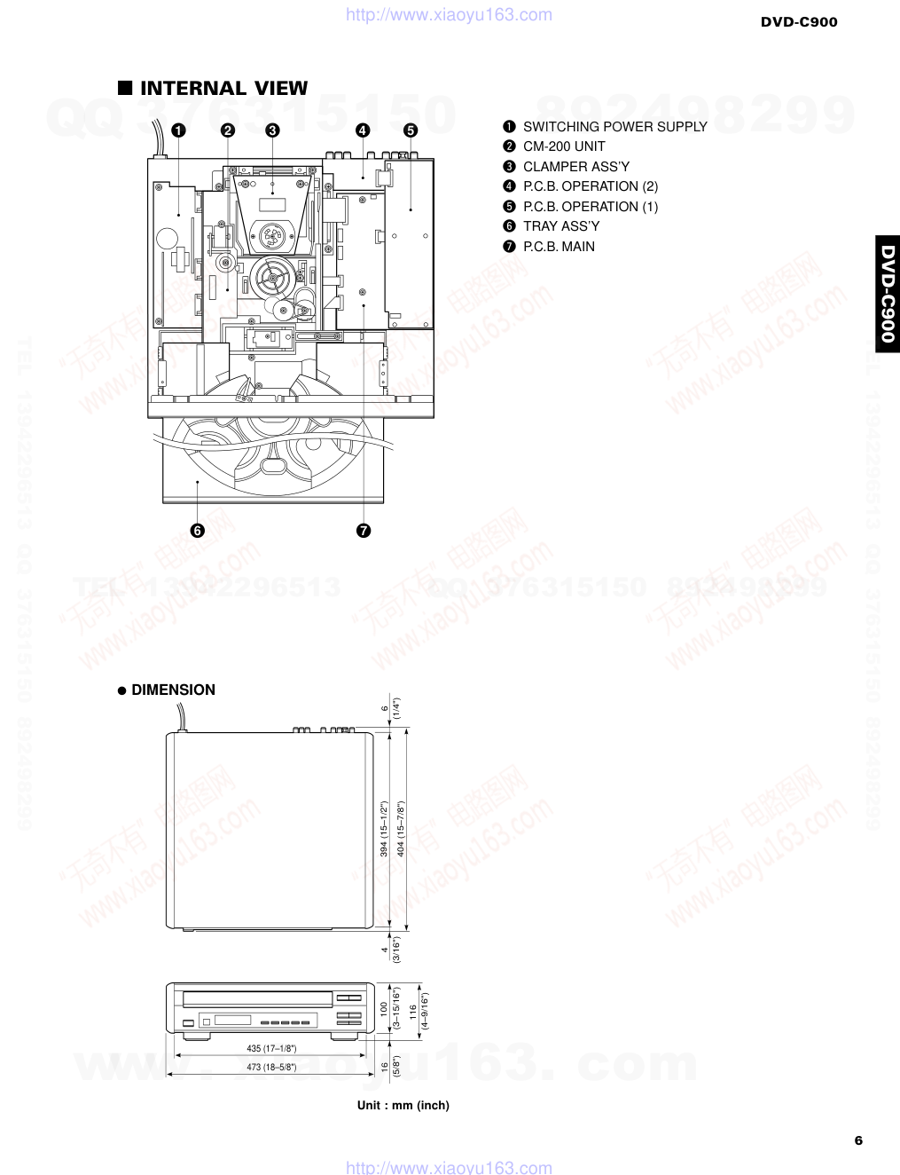
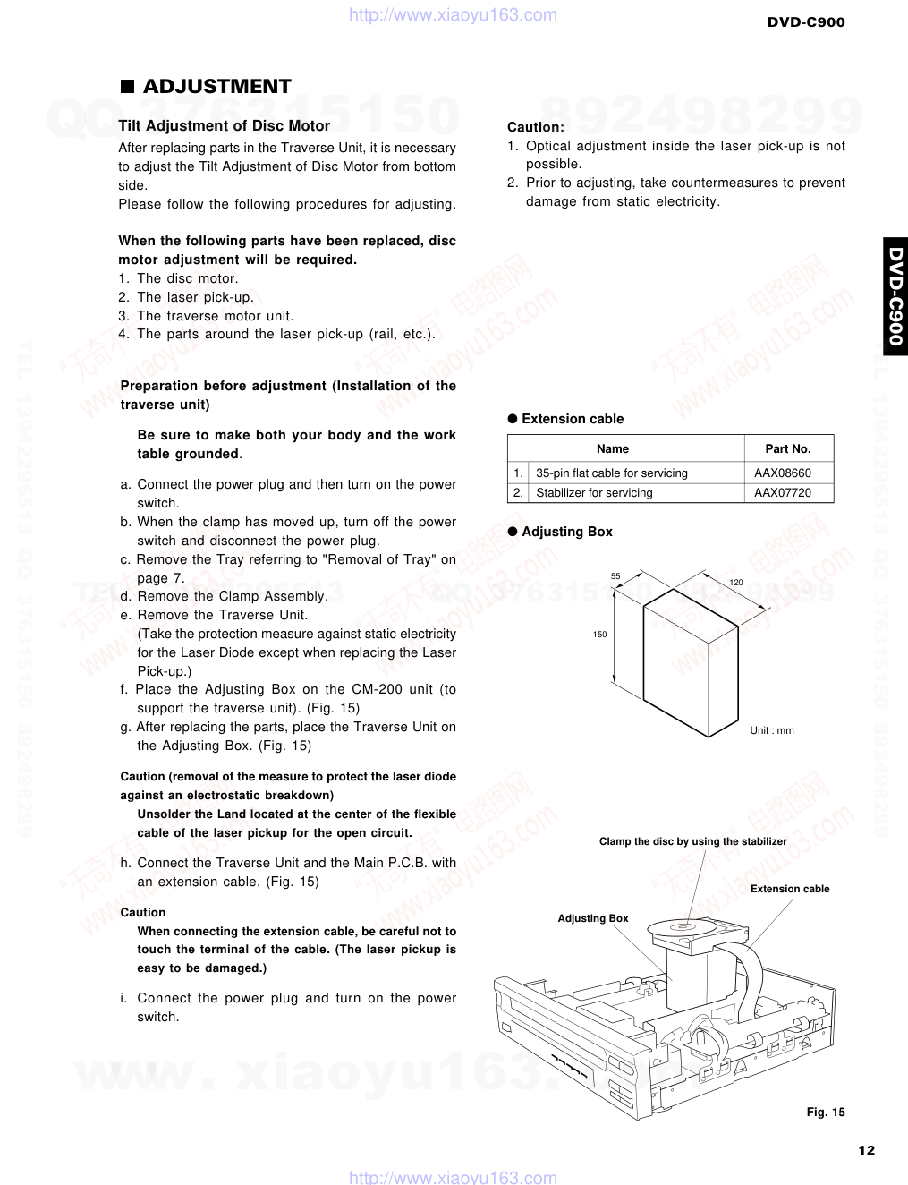
DVD-C900电路原理图
 "DVD-C900电路原理图-0")
 "DVD-C900电路原理图-1")
 "DVD-C900电路原理图-2")
 "DVD-C900电路原理图-3")
 "DVD-C900电路原理图-4")
 "DVD-C900电路原理图-5")
 "DVD-C900电路原理图-6")
 "DVD-C900电路原理图-7")
 "DVD-C900电路原理图-8")
 "DVD-C900电路原理图-9")
DVD-C900 DVD-C900 100653 SERVICE MANUAL DVD PLAYER This manual has been provided for the use of authorized YAMAHA Retailers and their service personnel. It has been assumed that basic service procedures inherent to the industry, and more specifically YAMAHA Products, are already known and understood by the users, and have therefore not been restated. WARNING: Failure to follow appropriate service and safety procedures when servicing this product may result in personal injury, destruction of expensive components, and failure of the product to perform as specified. For these reasons, we advise all YAMAHA product owners that any service required should be performed by an authorized YAMAHA Retailer or the appointed service representative. IMPORTANT: The presentation or sale of this manual to any individual or firm does not constitute authorization, certification or recognition of any applicable technical capabilities, or establish a principle-agent relationship of any form. The data provided is believed to be accurate and applicable to the unit(s) indicated on the cover. The research, engineering, and service departments of YAMAHA are continually striving to improve YAMAHA products. Modifications are, therefore, inevitable and specifications are subject to change without notice or obligation to retrofit. Should any discrepancy appear to exist, please contact the distributor's Service Division. WARNING: Static discharges can destroy expensive components. Discharge any static electricity your body may have accumulated by grounding yourself to the ground buss in the unit (heavy gauge black wires connect to this buss). IMPORTANT: Turn the unit OFF during disassembly and part replacement. Recheck all work before you apply power to the unit. IMPORTANT NOTICE DVD-C900 SERVICE MANUAL DISC MODE ANGLE RETURN MULTI SPEED TITLE/INDEX AUDIO SELECT SUBTITLE OFF/ON DVD1 TITLE MENU SET UP ON SCREEN STOP STILL/PAUSE 3 2 1 5 4 7 PLAY 6 +10 0 9 8 TIME OPEN/ CLOSE DISC SKIP CANCEL RANDOM PROG S/F REPEAT A-B SKIP/SEARCH www. xiaoyu163. com QQ 376315150 9 9 2 8 9 4 2 9 8 TEL 13942296513 9 9 2 8 9 4 2 9 8 0 5 1 5 1 3 6 7 3 Q Q TEL 13942296513 QQ 376315150 892498299 TEL 13942296513 QQ 376315150 892498299 http://www.xiaoyu163.com DVD-C900 DVD-C900 1. Critical Components Information. Components having special characteristics are marked and must be replaced with parts having specifications equal to those originally installed. 2. Leakage Current Measurement (For 120V Models Only). When service has been completed, it is imperative to verify that all exposed conductive surfaces are properly insulated from supply circuits. G Meter impedance should be equivalent to 1500 ohm shunted by 0.15µF. G Leakage current must not exceed 0.5mA. G Be sure to test for leakage with the AC plug in both polarities. EQUIPMENT UNDER TEST WALL OUTLET INSULATING TABLE AC LEAKAGE TESTER OR EQUIVALENT < CAUTION: USE OF CONTROLS OR ADJUSTMENTS OR PERFORMANCE OF PROCEDURES OTHER THAN THOSE SPECIFIED HEREIN MAY RESULT IN HAZARDOUS RADIATION EXPOSURE. THE COMPACT DISC PLAYER SHOULD NOT BE ADJUSTED OR REPAIRED BY ANYONE EXCEPT PROPERLY QUALIFIED SERVICE PERSONNEL. PROTECTION OF EYES FROM LASER BEAM DURING SERVICING I TO SERVICE PERSONNEL 1 This set employs a laser. Therefore, be sure to carefully follow the instructions below when servicing . 1. Pickup G Wave length : 655 nm G Laser power : CLASS II 2. When checking the laser diode emission, keep your eyes more than 30 cm away from the objective lens. I CONTENTS TO SERVICE PERSONNEL ......................................... 1 PREVENTION OF ELECTRO STATIC DISCHRGE (ESD) TO ELECTRO STATICALLY SENSITIVE (ES) DEVICES....................... 2 SPECIFICATIONS ......................................................... 3 REAR PANELS ............................................................. 4 PRECAUTION LASER DIODE ..................................... 5 HANDLING PRECAUTIONS FOR TRAVERS DECK .. 5 INTERNAL VIEW .......................................................... 6 DISASSEMBLY PROCEDURES .............................. 7~8 REPLACING THE MAIN PARTS OF THE TRAVERSE UNIT .. 9~10 GREASE APPLICATION DIAGRAM .......................... 10 MAIN P.C.B. OPERATION CHECK ........................... 11 ADJUSTMENT....................................................... 12~13 TEST MODE ..........................................................15~26 TROUBLESHOOTIG ............................................. 27~30 IC DATA ................................................................31~46 IC BLOCKS ...........................................................47~52 PIN CONNECTION DIAGRAM ................................... 52 DISPLAY DATA .......................................................... 53 BLOCK DIAGRAM ................................................54~55 PRINTED CIRCUIT BOARD ................................. 56~65 SCHEMATIC DIAGRAM ....................................... 66~68 PARTS LIST ..........................................................69~84 SWITCHING POWER SUPPLY ............................85~87 REMOTE CONTROL TRANSMITTER........................ 88 OPERATING INSTRUCTION ................................ 89~96 www. xiaoyu163. com QQ 376315150 9 9 2 8 9 4 2 9 8 TEL 13942296513 9 9 2 8 9 4 2 9 8 0 5 1 5 1 3 6 7 3 Q Q TEL 13942296513 QQ 376315150 892498299 TEL 13942296513 QQ 376315150 892498299 http://www.xiaoyu163.com DVD-C900 DVD-C900 WARNING: CHEMICAL CONTENT NOTICE! The solder used in the production of this product contains LEAD. In addition, other electrical/electronic and/or plastic (where applicable) components may also contain traces of chemicals found by the California Health and Welfare Agency (and possibly other entities) to cause cancer and/or birth defects or other reproductive harm. DO NOT PLACE SOLDER, ELECTRICAL/ELECTRONIC OR PLASTIC COMPONENTS IN YOUR MOUTH FOR ANY REASON WHATSOEVER! Avoid prolonged, unprotected contact between solder and your skin! When soldering, do not inhale solder fumes or expose eyes to solder/flux vapor! If you come in contact with solder or components located inside the enclosure of this product, wash your hands before handling food. 2 I PREVENTION OF ELECTRO STATIC DISCHARGE (ESD) TO ELECTRO STATICALLY SENSITIVE (ES) DEVICES www. xiaoyu163. com QQ 376315150 9 9 2 8 9 4 2 9 8 TEL 13942296513 9 9 2 8 9 4 2 9 8 0 5 1 5 1 3 6 7 3 Q Q TEL 13942296513 QQ 376315150 892498299 TEL 13942296513 QQ 376315150 892498299 http://www.xiaoyu163.com DVD-C900 DVD-C900 U ....... U.S.A. model R ....... General model T ....... China model Manufactured under license from Dolby Laboratories Licens- ing Corporation. "Dolby" and the double-D symbol V are trademarks of Dolby Laboratories Licensing Corporation. I SPECIFICATIONS 3 I AUDIO SECTION Frequency Response DVD (48kHz Sampling) 2 Hz to 22 KHz DVD (96kHz Sampling) 2 Hz to 44 KHz CD, Video CD 2 Hz to 20 KHz Harmonic Distortion+Noise (1kHz) 0.002% or less S/N Ratio 115 dB or more (Weighted) Dynamic Range DVD (48kHz, 24 bit) 104 dB or more CD, Video CD 100 dB or more Output Voltage (1 kHz, 0 dB) 2.0 ± 0.3V I VIDEO SECTION VIDEO output 1 Vp-p (75 ohms) S VIDEO output Y output 1 Vp-p (75 ohms) C output U model 0.286 Vp-p (75 ohms) R, T models 0.3 Vp-p (75 ohms) COMPONENT VIDEO output Y output 1 Vp-p (75 ohms) Pb output U model 0.648 Vp-p (75 ohms) R, T models 0.7 Vp-p (75 ohms) Pr output U model 0.648 Vp-p (75 ohms) R, T models 0.7 Vp-p (75 ohms) I GENERAL Power Requirements U model 120V, 60Hz T model 220V, 50Hz R model 110 to 240V, 50/60Hz Power Consumption 30W Dimensions (W x H x D) (Without side panels) 435 x 116 x 404 mm (17-1/8” x 4-9/16” x 15-7/8”) (With side panels) 473 x 116 x 404 mm (18-5/8” x 4-9/16” x 15-7/8”) Weight (Without side panels) 6.2 kg (13 lbs 10 oz) (With side panels) 7.2 kg (15 lbs 13 oz) Accessories Audio/video connection cord Remote control transmitter Dry-cell: x2 (Size “AA”, R06) * Specifications subject to change without notice. LOCALE MANAGEMENT INFORMATION Locale Management Information : This DVD player is designed and manufactured to respond to the Locale Management Information that is recorded on a DVD disc. If the Locale number described on the DVD disc does not correspond to the Locale number of this DVD player, this DVD player cannot play this disc. This product incorporates copyright protection technology that is protected by method claims of certain U.S. patents and other intellectual property rights owned by Macrovision Corporation and other rights owners. Use of this copyright protection technology must be authorized by Macrovision Corporation, and is intended for home and other limited viewing uses only unless otherwise authorized by Macrovision Corporation. Reverse engineering or disassembly is prohibited. q w r w t t r w y e t www. xiaoyu163. com QQ 376315150 9 9 2 8 9 4 2 9 8 TEL 13942296513 9 9 2 8 9 4 2 9 8 0 5 1 5 1 3 6 7 3 Q Q TEL 13942296513 QQ 376315150 892498299 TEL 13942296513 QQ 376315150 892498299 http://www.xiaoyu163.com DVD-C900 DVD-C900 I REAR PANELS M U model M R model M T model 4 www. xiaoyu163. com QQ 376315150 9 9 2 8 9 4 2 9 8 TEL 13942296513 9 9 2 8 9 4 2 9 8 0 5 1 5 1 3 6 7 3 Q Q TEL 13942296513 QQ 376315150 892498299 TEL 13942296513 QQ 376315150 892498299 http://www.xiaoyu163.com DVD-C900 DVD-C900 5 I PRECAUTION LASER DIODE I HANDLING PRECAUTIONS FOR TRAVERS DECK www. xiaoyu163. com QQ 376315150 9 9 2 8 9 4 2 9 8 TEL 13942296513 9 9 2 8 9 4 2 9 8 0 5 1 5 1 3 6 7 3 Q Q TEL 13942296513 QQ 376315150 892498299 TEL 13942296513 QQ 376315150 892498299 http://www.xiaoyu163.com DVD-C900 DVD-C900 6 I INTERNAL VIEW 4 3 2 1 5 6 7 435 (17–1/8") 473 (18–5/8") 100 (3–15/16") 16 (5/8") 116 (4–9/16") 4 (3/16") 6 (1/4") 394 (15–1/2") 404 (15–7/8") G DIMENSION Unit : mm (inch) q SWITCHING POWER SUPPLY w CM-200 UNIT e CLAMPER ASS’Y r P.C.B. OPERATION (2) t P.C.B. OPERATION (1) y TRAY ASS’Y u P.C.B. MAIN www. xiaoyu163. com QQ 376315150 9 9 2 8 9 4 2 9 8 TEL 13942296513 9 9 2 8 9 4 2 9 8 0 5 1 5 1 3 6 7 3 Q Q TEL 13942296513 QQ 376315150 892498299 TEL 13942296513 QQ 376315150 892498299 http://www.xiaoyu163.com 1 2 3 4 5 6 7 88 DVD-C900 REMOTE CONTROL TRANSMITTER I SCHEMATIC DIAGRAM R1 2.2Ω KI/O6 KI/O7 S0 REM VDD X–OUT X–IN VSS KI/O5 KI/O4 KI/O3 KI/O2 KI/O1 KI/O0 KI3 KI2 KI1 KI0 1 2 3 4 5 6 7 8 9 10 20 19 18 17 16 15 14 13 12 11 IC1 µPD63AGS–442 X1 3.64MHz D1 Q1 IED1 C1 47µF RESET K1 K2 K4 K3 K5 K6 K7 K8 K9 K10 K12 K11 K13 K14 K15 K16 K17 K18 K20 K19 K21 K22 K23 K25 K26 K28 K27 K29 K30 K31 K34 K36 K24 K39 K41 K35 K43 K44 K33 K38 K37 S1/LED 1 2 3 4 5 6 7 8 9 10 11 12 13 14 15 16 17 18 19 20 21 22 23 24 25 26 27 28 29 30 31 33 34 35 36 37 38 39 41 43 44 OPEN/CLOSE CANCEL S/F REPEAT A–B REPEAT RANDOM PROG 1 2 3 4 5 6 7 8 9 0 +10 ANGLE h RETURN TITLE/INDEX SET UP SKIP/SEARCH t SKIP/SEARCH y OFF/ON TITLE q SELECT w AUDIO MENU g MULTI SPEED SUBTITLE ON SCREEN STOP a STILL/PAUSE d PLAY w DISC SKIP DISC MODE TIME 7C 7C 7C 7C 7C 7C 7C 7C 7C 7C 7C 7C 7C 7C 7C 7C 7C 7C 7C 7C 7C 7C 7C 7C 7C 7C 7C 7C 7C 7C 7C 7C 7C 7C 7C 7C 7C 7C 7C 7C 7C 81 9F A3 A4 A1 A0 94 95 96 97 98 99 9A 9B 9C 93 9D AE B4 B7 9E AC B9 BA AA B1 B5 B8 B6 AD B2 B3 BB AB A6 85 83 82 8B BC A8 FUNCTION Key No. CUSTOM (HEX) DATA (HEX) DISC MODE ANGLE RETURN MULTI SPEED TITLE/INDEX AUDIO SELECT SUBTITLE OFF/ON DVD1 TITLE MENU SET UP ON SCREEN STOP STILL/PAUSE 3 2 1 5 4 7 PLAY 6 +10 0 9 8 TIME OPEN/ CLOSE DISC SKIP CANCEL RANDOM PROG S/F REPEAT A-B SKIP/SEARCH A B C D E www. xiaoyu163. com QQ 376315150 9 9 2 8 9 4 2 9 8 TEL 13942296513 9 9 2 8 9 4 2 9 8 0 5 1 5 1 3 6 7 3 Q Q TEL 13942296513 QQ 376315150 892498299 TEL 13942296513 QQ 376315150 892498299 http://www.xiaoyu163.com DVD-C900 DVD-C900 www. xiaoyu163. com QQ 376315150 9 9 2 8 9 4 2 9 8 TEL 13942296513 9 9 2 8 9 4 2 9 8 0 5 1 5 1 3 6 7 3 Q Q TEL 13942296513 QQ 376315150 892498299 TEL 13942296513 QQ 376315150 892498299 http://www.xiaoyu163.com DVD-C900 DVD-C900 12 I ADJUSTMENT Tilt Adjustment of Disc Motor After replacing parts in the Traverse Unit, it is necessary to adjust the Tilt Adjustment of Disc Motor from bottom side. Please follow the following procedures for adjusting. When the following parts have been replaced, disc motor adjustment will be required. 1. The disc motor. 2. The laser pick-up. 3. The traverse motor unit. 4. The parts around the laser pick-up (rail, etc.). G Extension cable 1. 35-pin flat cable for servicing AAX08660 2. Stabilizer for servicing AAX07720 Name Part No. G Adjusting Box Extension cable Adjusting Box 120 55 150 Unit : mm Caution: 1. Optical adjustment inside the laser pick-up is not possible. 2. Prior to adjusting, take countermeasures to prevent damage from static electricity. Preparation before adjustment (Installation of the traverse unit) Be sure to make both your body and the work table grounded. a. Connect the power plug and then turn on the power switch. b. When the clamp has moved up, turn off the power switch and disconnect the power plug. c. Remove the Tray referring to "Removal of Tray" on page 7. d. Remove the Clamp Assembly. e. Remove the Traverse Unit. (Take the protection measure against static electricity for the Laser Diode except when replacing the Laser Pick-up.) f. Place the Adjusting Box on the CM-200 unit (to support the traverse unit). (Fig. 15) g. After replacing the parts, place the Traverse Unit on the Adjusting Box. (Fig. 15) Caution (removal of the measure to protect the laser diode against an electrostatic breakdown) Unsolder the Land located at the center of the flexible cable of the laser pickup for the open circuit. h. Connect the Traverse Unit and the Main P.C.B. with an extension cable. (Fig. 15) Caution When connecting the extension cable, be careful not to touch the terminal of the cable. (The laser pickup is easy to be damaged.) i. Connect the power plug and turn on the power switch. Fig. 15 Clamp the disc by using the stabilizer www. xiaoyu163. com QQ 376315150 9 9 2 8 9 4 2 9 8 TEL 13942296513 9 9 2 8 9 4 2 9 8 0 5 1 5 1 3 6 7 3 Q Q TEL 13942296513 QQ 376315150 892498299 TEL 13942296513 QQ 376315150 892498299 http://www.xiaoyu163.com DVD-C900 DVD-C900 13 Adjustment Procedures After Adjusting Check the following 1. After adjusting by the DVD test disc, play a video CD or CD-DA and check that there is no abnormal operation. 1. Play back the DVD test disc and then place the unit in play mode with title 8, then push the Pause button. 2. At first, Adjust Tangential Adjustment Screw then adjust Tilt Adjustment Screw with the Hex Wrench (2.0 mm) from bottom side. Repeat 2 to 3 times alternately until the waveform at JIT OUT indicated below is obtained. Final adjustment should be Tilt Adjustment. G The valley sections of the waveform should be as flat as possible. G The total DC level should be obtained minimized as much as possible. G The waveform whisker sections will not disappear. Measurement Point Adjustment Point Mode Test Disc Measuring Equipment Adjustment Value JIT OUT Tangential ADJ. screw Play DVDT-S01 Oscilloscope Adjust untill the bottom section (See page 14) Tilt ADJ. screw (title 8) DC 500 mV/div of the waveform becomes flat and Pause 20 msec/div the DC components are minimum. 1. DVD disc DVDT-S01 TX946080 2. VIDEO-CD/CD-DA disc PVCD-K06 TX946090 Type Test disc Part No. G Test Disc Tangential ADJ. Screw Tilt ADJ. Screw Use a hex. wrench (2.0mm) OK NG DC range 500mV/div 20msec/div 0V 0V DC renge 500mV/div 20msec/div JIT OUT (See page 14) www. xiaoyu163. com QQ 376315150 9 9 2 8 9 4 2 9 8 TEL 13942296513 9 9 2 8 9 4 2 9 8 0 5 1 5 1 3 6 7 3 Q Q TEL 13942296513 QQ 376315150 892498299 TEL 13942296513 QQ 376315150 892498299 http://www.xiaoyu163.com DVD-C900 DVD-C900 14 J, R, T only 1 1 25 75 51 26 50 100 76 25 26 50 100 76 75 51 57 84 85 112 56 29 28 1 22 1 1 1 4 8 5 7 14 8 1 1 1 1 52 156 105 1 4 8 5 1 44 132 133 176 88 45 89 53 104 208 157 25 50 26 10 20 11 1 10 20 11 4 8 5 23 44 JIT OUT FE TE www. xiaoyu163. com QQ 376315150 9 9 2 8 9 4 2 9 8 TEL 13942296513 9 9 2 8 9 4 2 9 8 0 5 1 5 1 3 6 7 3 Q Q TEL 13942296513 QQ 376315150 892498299 TEL 13942296513 QQ 376315150 892498299 http://www.xiaoyu163.com DVD-C900 DVD-C900 I TEST MODE 15 This built-in test mode is to facilitate inspection, measurement and locating any faulty point. 1. How to start the Test mode Before operation Use the key operation When the product mode at stop Press the ANGLE key on the remote control unit while pressing the STOP key on the panel. 2. Display at starting of the Test mode When the Test mode is set, the sub-mode [1] appears as shown below. Test mode (sub-mode [1]) Test mode (sub-mode [1]) Current sub-mode No. is indicated here. Panel LED display • All LEDs turn off. 3. How to restore the Product mode Precaution • The product mode means the mode in which the normal player operation is available. • To restore the Product mode from the Test mode, it is necessary to turn off the power once. Item Condition before operation Key operation To restore the Product mode Test mode Panel POWER OFF ^ Panel POWER ON Condition immediately after the Product mode is restored • Immediately after the Product mode is restored, the memory of the table position is initialized. 5 4 3 2 1 Item Test Laser Diode ON Focus Servo ON Focus Jump 1-2 Focus Jump 2-1 Track. Servo OFF Spindle Rot +/- Slide In/Out Clamp Up/Down Tray Open/Close Panel Display RETURN TITLE/INDEX SUBTITLE OFF/ON MULTI SPEED DISC MODE/TIME SKIP/SEARCH -/+ Up/Down OPEN/CLOSE ANGLE PLAY STOP Play Stop Prev.Page Next Page Q W www. xiaoyu163. com QQ 376315150 9 9 2 8 9 4 2 9 8 TEL 13942296513 9 9 2 8 9 4 2 9 8 0 5 1 5 1 3 6 7 3 Q Q TEL 13942296513 QQ 376315150 892498299 TEL 13942296513 QQ 376315150 892498299 http://www.xiaoyu163.com DVD-C900 DVD-C900 16 Power OFF state Test mode Product mode POWER OFF on panel POWER OFF on panel POWER ON on panel STOP on panel & ANGLE on remote control unit 4. Sub mode • There are 2 sub modes for the Test mode. • Immediately after starting the Test mode, the sub mode [1] is set. • For the details of each sub mode, refer to Ref. page. Sub mode Description Ref. page 1 Individual operation check 17 2 Log display 24 Selection of sub mode Press the desired sub mode No. on ten keys of the remote control unit while pressing the STOP button on the panel. Sub mode [1] : Individual operation check The current sub mode No. is indicated here. Sub mode [2] : Log display 5 4 3 2 1 5 4 3 2 1 Item Test Laser Diode ON Focus Servo ON Focus Jump 1-2 Focus Jump 2-1 Track. Servo OFF Spindle Rot +/- Slide In/Out Clamp Up/Down Tray Open/Close Panel Display RETURN TITLE/INDEX SUBTITLE OFF/ON MULTI SPEED DISC MODE/TIME SKIP/SEARCH -/+ Up/Down OPEN/CLOSE ANGLE PLAY STOP Play Stop Prev.Page Next Page Q W Log Display 00 0163EAEC 13 81AE -------------------- 01 0163EAEA 13 80C8 -------------------- 02 0163EAD8 13 81AC -------------------- 03 0163EAC4 13 81B8 -------------------- 04 0163EABF 13 81B3 -------------------- ------------------------ ------------------------ ------------------------ ------------------------ ------------------------ ------------------------ ------------------------ ------------------------ ------------------------ ------------------------ SKIP/SEARCH Log Switch Prev.Page Next Page Q W Event Log www. xiaoyu163. com QQ 376315150 9 9 2 8 9 4 2 9 8 TEL 13942296513 9 9 2 8 9 4 2 9 8 0 5 1 5 1 3 6 7 3 Q Q TEL 13942296513 QQ 376315150 892498299 TEL 13942296513 QQ 376315150 892498299 http://www.xiaoyu163.com DVD-C900 DVD-C900 17 5 Details of sub mode [1] Sub mode [1] : Individual operation check • functions included in the player are checked individually. • The sub mode [1] is set immediately after starting the Test mode. The number of the item being executed is displayed here. Even after completing execution, the display remains until the procedure to execute the next test is taken. 5 4 3 2 1 List of sub mode [1] Function No. Item Key operation Basic control 000 Stop operation STOP 001 Play operation PLAY/PAUSE or PLAY on remote control unit Laser diode control 010 Laser diode ON RETURN on remote control unit Focus control 020 Focus servo ON TITLE/INDEX on remote control unit 021 Focus jump 1 layer ^ 2 layers SUBTITLE on remote control unit 022 Focus jump 2 layers ^ 1 layer OFF/ON on remote control unit Track kick control 030 Tracking servo OFF MULTI SPEED on remote control unit Spindle control 040 Spindle rotation in + direction DISC MODE on remote control unit 041 Spindle rotation in - direction TIME on remote control unit Traverse control 050 Traverse moving to innermost track SKIP/SEARCH - 051 Traverse moving to outermost track SKIP/SEARCH + Clamp control 060 Clamp down H on remote control unit 061 Clamp up G on remote control unit Disc tray control 070 Disc tray open OPEN/CLOSE 071 Disc tray close OPEN./CLOSE Panel display 080 Test pattern 1 ANGLE on remote control unit (FL, LED) 081 Test pattern 2 ANGLE on remote control unit 082 Test pattern 3 ANGLE on remote control unit 083 Test pattern 4 ANGLE on remote control unit 084 Normal display of test mode ANGLE on remote control unit Tracking control 090 1 track kick continued in - direction 1 on remote control unit 091 1 track kick continued in + direction 2 on remote control unit 092 30 track kick continued in - direction 3 on remote control unit 093 30 track kick continued in + direction 4 on remote control unit 094 150 track kick continued in - direction 5 on remote control unit 095 150 track kick continued in + direction 6 on remote control unit 096 Still kick continued in - direction 7 on remote control unit 097 Still kick continued in + direction 8 on remote control unit Turntable control 100 Disc skip in + direction +10 ^ 1 on remote control unit 101 Disc skip in - direction +10 ^ 2 on remote control unit 102 High speed clockwise table rotation continued +10 ^ 3 on remote control unit 103 High speed counterclockwise table rotation continued +10 ^ 4 on remote control unit 104 Low speed clockwise table rotation continued +10 ^ 5 on remote control unit 105 Low speed counterclockwise table rotation continued +10 ^ 6 on remote control unit FE operation mode setting 110 DVD operation mode setting REPEAT S/F on remote control unit 111 VCD/CD-DA operation mode setting A-B on remote control unit 112 Disc playback setting step 1 Panel DISC 2 113 Disc playback setting step 2 Panel DISC 3 114 Disc playback setting step 3 Panel DISC 4 Image output test 120 Color bar image output ON SCREEN on remote control unit Caution With PLAY operated in the test mode, even when the disc is played, the audio and video signals of the disc are not output from the audio/video output terminal. (The superimposed image of the sub-mode [1] remains as it is.) www. xiaoyu163. com QQ 376315150 9 9 2 8 9 4 2 9 8 TEL 13942296513 9 9 2 8 9 4 2 9 8 0 5 1 5 1 3 6 7 3 Q Q TEL 13942296513 QQ 376315150 892498299 TEL 13942296513 QQ 376315150 892498299 http://www.xiaoyu163.com DVD-C900 DVD-C900 18 Bottom Bottom OSD (On Screen Display) • A list of key operations used when checking individual operation appears on the screen. • Page 1 appears immediately after the mode is shifted to sub mode [1]. There are 5 pages in all. • The pages on the screen can be changed. Key operation Function W on remote control unit The page on the screen advances to the next page. Q on remote control unit The page on the screen moves back to the previous page. Page 1 A list of test items and key operations is displayed here. The key operation method for basic operation is displayed. Page changing (to previous/next page) method is displayed. Note 1 : There is no relation between the screen display and the key operation being accepted. Regardless of the menu currently on screen, all key operations are accepted. Note 2 : The page can be always changed even when an item is currently executed. Item Test Laser Diode ON Focus Servo ON Focus Jump 1-2 Focus Jump 2-1 Track. Servo OFF Spindle Rot +/- Slide In/Out Clamp Up/Down Tray Open/Close Panel Display RETURN TITLE/INDEX SUBTITLE OFF/ON MULTI SPEED DISC MODE/TIME SKIP/SEARCH -/+ Up/Down OPEN/CLOSE ANGLE PLAY STOP Play Stop Prev.Page Next Page Q W Page 2 Page 3 Page 4 Page 5 Item Test Track Kick -1 Track Kick +1 Track Kick -30 Track Kick +30 Track Kick -150 Track Kick +150 Still Kick - Still Kick + 1 2 3 4 5 6 7 8 PLAY STOP Play Stop Prev.Page Next Page Q W Item Test Disc Skip + Disc Skip - Table Rot. + Fast Table Rot. - Fast Table Rot. + Slow Table Rot. - Slow + 10. 1 + 10. 2 + 10. 3 + 10. 4 + 10. 5 + 10. 6 PLAY STOP Play Stop Prev.Page Next Page Q W Item Test Color Bar Output ON SCREEN PLAY STOP Play Stop Prev.Page Next Page Q W Item Test FE DVD Mode FE VCD/CDDA Mode Setup Step 1 Setup Step 2 Setup Step 3 S/F A-B DISC 2 DISC 3 DISC 4 PLAY STOP Play Stop Prev.Page Next Page Q W www. xiaoyu163. com QQ 376315150 9 9 2 8 9 4 2 9 8 TEL 13942296513 9 9 2 8 9 4 2 9 8 0 5 1 5 1 3 6 7 3 Q Q TEL 13942296513 QQ 376315150 892498299 TEL 13942296513 QQ 376315150 892498299 http://www.xiaoyu163.com DVD-C900 DVD-C900 1) Basic control • Basic operation used in the Test mode Item Key operation Description Stop operation STOP on panel or STOP on remote control unit Test operation being executed currently is stopped. (Test mode in the initial state) (*1) • When operating from DISC2 to DISC3 and from DISC3 to DISC4 on the panel, leave about a 5-seconds interval between operations. • If the focus servo function of the DVD 2-layer disc or the like does not turn on (no sound is heard from the focus actuator) even when DISC3 is operated on the panel, repeat operation of DISC3 on the panel at 5 seconds’ interval until the focus servo function turns on. • With PLAY operated in the test mode, even when the disc is played, the audio and video signals of the disc are not output from the audio/video output terminal.(The image remains superimposed in the sub-mode[1].) Stop Play “000” is indicated. “0:00:00” is indicated. “001” is indicated. 5 4 3 2 1 5 4 3 2 1 2) Laser diode control • Operation used to control the laser diode Item Key operation Description Focus servo ON TITLE/INDEX on remote control unit The focus servo is turned ON and the focus search function is started. Focus jump 1 layer ^ 2 layers SUBTITLE on remote control unit Focus jump from 1 layer to 2 layers is executed on DVD2-layer disc. Focus jump 2 layers ^ 1 layer OFF/ON on remote control unit Focus jump from 2 layers to 1 layer is executed on DVD2-layer disc. Item Key operation Description Laser diode ON RETURN on remote control unit The laser diode it turned ON. Note : To turn OFF the laser diode, press the STOP key on the panel or the remote control unit. 3) Focus control • Operation to control the focus servo. Note : To turn OFF the focus servo, press the STOP key on the panel or the remote control unit. 19 After setting to DVD operation mode or VCD/CD-DA operation mode in FE operation mode, operate DISC2, DISC3 and DISC4 on the panel in that order. (*1) PLAY/PAUSE on panel or PLAY on remote control unit Play operation (1) Play operation (2) The disc is played from the STOP state. The disc is played from the tracking servo OFF (See 4. Tracking control) or track kick continued (See 10. Track kick control) state while the disc is being played. www. xiaoyu163. com QQ 376315150 9 9 2 8 9 4 2 9 8 TEL 13942296513 9 9 2 8 9 4 2 9 8 0 5 1 5 1 3 6 7 3 Q Q TEL 13942296513 QQ 376315150 892498299 TEL 13942296513 QQ 376315150 892498299 http://www.xiaoyu163.com DVD-C900 DVD-C900 4) Tracking control • Operation to control the tracking servo Item Key operation Description Tracking servo OFF MULTI SPEED on remote control unit The tracking servo is turned OFF. Note : In order to turn ON the tracking servo, press the PLAY/PAUSSE key on the panel or the PLAY key on the remote control unit. 5) Spindle control • Operation to control the spindle motor Item Key operation Description Spindle rotation in + direction DISC MODE on remote control unit The spindle motor is run in the + direction continuously. Spindle rotation in - direction TIME on remote control unit The spindle motor is run in the - direction momentarily. Note 1 : In order to turn ON the spindle servo, press the PLAY/PAUSE key on the panel or the PLAY key on the remote control unit. Note 2 : In order to turn OFF the spindle servo, press the STOP key on the panel or the remote control unit. 6) Traverse control • Operation to control the traverse mechanical unit Item Key operation Description Traverse moving to innermost track SKIP/SEARCH - The traverse mechanical unit is moved to the innermost track and stopped when the innermost track limit switch is turned ON. Traverse moving to outermost track SKIP/SEARCH + The traverse mechanical unit is moved to the outermost track. It does not stop automatically even when it has reached the outermost track. 7) Clamp control • Operation to control the clamp mechanical unit. Item Key operation Description Clamp up H on remote control unit The clamp mechanical unit is moved up. Clamp down G on remote control unit The clamp mechanical unit is moved down. 8) Disc tray control • Operation to check the disc tray operation. Item Key operation Description Disc tray open OPEN/CLOSE The disc tray is opened. Disc tray close OPEN/CLOSE The disc tray is closed. If the disc tray has stopped midway, close operation is used. 20 www. xiaoyu163. com QQ 376315150 9 9 2 8 9 4 2 9 8 TEL 13942296513 9 9 2 8 9 4 2 9 8 0 5 1 5 1 3 6 7 3 Q Q TEL 13942296513 QQ 376315150 892498299 TEL 13942296513 QQ 376315150 892498299 http://www.xiaoyu163.com DVD-C900 DVD-C900 9) Panel display • Operation to check panel display • Two types of the panel display, FL and LED, are both tested at the same time. Item Condition before operation Key operation Condition after operation Test pattern 1 Normal display of test mode ANGLE on remote control unit Test pattern 1 Test pattern 2 Test pattern 1 ANGLE on remote control unit Test pattern 2 Test pattern 3 Test pattern 2 ANGLE on remote control unit Test pattern 3 Test pattern 4 Test pattern 3 ANGLE on remote control unit Test pattern 4 Normal display of test mode Test pattern 4 ANGLE on remote control unit Normal display of test mode Panel display test Item FL LED All segments light up. Test pattern 1 ALL LEDs light up. Test pattern 2 All numeric values and disc No. segments light up. LEDs 1, 3 and 5 light up, LEDs 2, 4 and AUTO DISPLAY OFF turn off. Test pattern 3 All segments other tan numeric values and disc No. light up. LEDs 2, 4 and AUTO DISPLAY OFF light up and LEDs 1, 3 and 5 turn off. Test pattern 4 All segments turn OFF. All LEDs turn OFF. 5 4 3 2 1 5 4 3 2 1 21 www. xiaoyu163. com QQ 376315150 9 9 2 8 9 4 2 9 8 TEL 13942296513 9 9 2 8 9 4 2 9 8 0 5 1 5 1 3 6 7 3 Q Q TEL 13942296513 QQ 376315150 892498299 TEL 13942296513 QQ 376315150 892498299 http://www.xiaoyu163.com DVD-C900 DVD-C900 10) Track kick control • This mode is used to check the track kick operation. Item Key operation Description 1 track kick continued in - direction 1 on remote control unit Kicking is continued for 1 track in the - direction. 1 track kick continued in + direction 2 on remote control unit Kicking is continued for 1 track in the + direction. 30 track kick continued in - direction 3 on remote control unit Kicking is continued for 30 tracks in the - direction. 30 track kick continued in + direction 4 on remote control unit Kicking is continued for 30 tracks in the + direction. 150 track kick continued in - direction 5 on remote control unit Kicking is continued for 150 tracks in the - direction. 150 track kick continued in + direction 6 on remote control unit Kicking is continued for 150 tracks in the + direction. Still kick continued in - direction 7 on remote control unit Still kicking is continued in the - direction. Still kick continued in + direction 8 on remote control unit Still kicking is continued in the + direction Note : In order to cancel track kicking, press the STOP key on the panel of remote control unit, PLAY/PAUSE key on the panel, or the PLAY key on the remote control unit. Track kicking 5 4 3 2 1 11) Turntable control • This mode is used to check the turntable operation. Item Key operation Description Disk skip in + direction +10 ^ 1 on remote control unit The turntable is rotated clockwise for 1 disc. Disk skip in - direction +10 ^ 2 on remote control unit The turntable is rotated counterclockwise for 1 disc. High speed clockwise table rotation continued +10 ^ 3 on remote control unit Clockwise rotation of the turntable is continued at a high speed. High speed counterclockwise table rotation continued +10 ^ 4 on remote control unit Counterclockwise rotation of the turntable is continued at a high speed. Low speed clockwise table rotation continued +10 ^ 5 on remote control unit Clockwise rotation of the turntable is continued at a low speed. Low speed counterclockwise table rotation continued +10 ^ 6 on remote control unit Counterclockwise rotation of the turntable is continued at a low speed. +/- direction disc skip 5 4 3 2 1 “0:00:00” is indicated here. 22 Precaution : Be sure to perform the clamp-down procedure before running the table. (*2) (*2) (*2) (*2) (*2) www. xiaoyu163. com QQ 376315150 9 9 2 8 9 4 2 9 8 TEL 13942296513 9 9 2 8 9 4 2 9 8 0 5 1 5 1 3 6 7 3 Q Q TEL 13942296513 QQ 376315150 892498299 TEL 13942296513 QQ 376315150 892498299 http://www.xiaoyu163.com DVD-C900 DVD-C900 12) FE operation mode setting • This mode is used to set the FE operation mode Item Key operation Description DVD operation mode setting REPEAT S/F on remote control unit FE is set for the DVD playback enable mode. VCD/CD-DA operation mode setting REPEAT A-B on remote control unit FE is set for the VCD/CD-DA playback enable mode. Disc playback setting step 1 Panel DISC 2 (*1) The setting required for disc playback is executed. (Step 1) Disc playback setting step 2 Panel DISC 3 (*1) The setting required for disc playback is executed. (Step 2) Disc playback setting step 3 Panel DISC 4 (*1) The setting required for disc playback is executed. (Step 3) 13) Image output test Item Key operation Description Color bar image output ON SCREEN on remote control unit The color bar image is output. 6 Details of sub mode [2] Sub mode [2] : Log display • Press the 2 key on the remote control unit while pressing the STOP key on the panel. • Various logs controlled in the player FE appear on the screen. • Three types of logs are displayed; event log, error log and timer log. • Immediately after this sub mode has been set, the event log (page 1) is displayed. • The type of the log on display (event, error or timer) can be changed. • When the page is changed while the event log or the error log is displayed, all log display becomes available. Key operation Description SKIP/SEARCH + on remote control unit The display is changed to the next log. SKIP/SEARCH - on remote control unit The display is changed to the previous log. W on remote control unit The display is changed to the next page. Q on remote control unit The display is changed to the previous page. 23 (*1) • When operating from DISC2 to DISC3 and from DISC3 to DISC4 on the panel, leave about a 5-seconds interval between operations. www. xiaoyu163. com QQ 376315150 9 9 2 8 9 4 2 9 8 TEL 13942296513 9 9 2 8 9 4 2 9 8 0 5 1 5 1 3 6 7 3 Q Q TEL 13942296513 QQ 376315150 892498299 TEL 13942296513 QQ 376315150 892498299 http://www.xiaoyu163.com DVD-C900 DVD-C900 Event log display • The event log screen shows 5 event logs for each page. There are up to 50 pages. Log Display 00 0163EAEC 13 81AE -------------------- 01 0163EAEA 13 80C8 -------------------- 02 0163EAD8 13 81AC -------------------- 03 0163EAC4 13 81B8 -------------------- 04 0163EABF 13 81B3 -------------------- ------------------------ ------------------------ ------------------------ ------------------------ ------------------------ ------------------------ ------------------------ ------------------------ ------------------------ ------------------------ SKIP/SEARCH Log Switch Prev.Page Next Page Q W Event Log Operation method to change to previous/next page Extended log information for extended block 3 Extended log information for extended block 1 Extended log information for extended block 2 Log No. Accumulated energized time (*1) during log recording Log task No. Basic log information Operation method to change log Log type Error log display • The error log screen shows 5 error logs for each page. There are up to 12 pages. Log Display 00 0160FF3F 13 0200 EE0302ED0000 01 0160FF3F 13 8300 -------------------- 02 014B8604 17 F601 25346A2210EF 03 014B8601 13 0200 6A2210EF0000 04 014B8601 13 8200 -------------------- 000302B30302 -------------------- 800000040000 -------------------- 2210F0220ED2 -------------------- 00220ED22534 -------------------- 800000040000 -------------------- SKIP/SEARCH Log Switch Prev.Page Next Page Q W Error Log Log Display System Timer Laser Timer Clamp Counter 0163F0A7 00B29A98 00000ABF SKIP/SEARCH Log Switch Prev.Page Next Page Q W Timer Log Accumulated energized time when obtaining timer log Laser timer Counted number of clamp mechanical unit operation (Clamping and unclamping are counted as 1 time each.) Timer log display • The timer log screen has 1 page. Note 1 : All numeric values including the log No. are displayed in hexadecimal. Note 2 : When displaying the basic log information, the upper byte is used as the basic log information 1. Note 3 : When displaying the extended log information, the uppermost byte is used as the extended log information 1 and the lowermost byte as the extended log information 6. Note 4 : If no extended block exists, "----------" should be used to display the extended log information of the applicable extended block. 5 4 3 2 1 Represents sub mode No. Log type Represented by Event log "001" Error log "002" Timer log "003" Represents log type. "0:00:00" on display constantly. 24 (*1) "1" = 160 ms "FF" = 255 x 160 ms "100" = 256 x 160 ms "177" = 375 x 160 ms = 1 minute www. xiaoyu163. com QQ 376315150 9 9 2 8 9 4 2 9 8 TEL 13942296513 9 9 2 8 9 4 2 9 8 0 5 1 5 1 3 6 7 3 Q Q TEL 13942296513 QQ 376315150 892498299 TEL 13942296513 QQ 376315150 892498299 http://www.xiaoyu163.com DVD-C900 DVD-C900 Clearing log • The data of each log (event, error or timer) can be cleared individually. • In case of the timer log, the data is cleared by items. • Before executing the clear command, a message to confirm execution of the clear function appears. • On the screen after the clear function has been executed, the value which has been cleared appears. To clear the event log a. Using SKIP/SEARCH +/-, have the event log screen displayed. b. Press the CANCEL key on the remote control unit. Then a message to confirm execution of the clear function appears on the screen. Event log clear confirmation screen Note: When the message appears, "NO" is selected (highlighted). Select "YES" or "NO" by using H and G keys. The highlight moves as H and G keys are operated. Pressing the SELECT key will finalize the selection. Log Display Are you sure? Yes No SELECT H G Clear Event Log Set Log Display Are you sure? Yes No SELECT H G Clear Error Log Set To clear the error log a. Using SKIP/SEARCH +/-, have the error log screen displayed. b. Press the CANCEL key on the remote control unit. Then a message to confirm execution of the clear function appears on the screen. Error log clear confirmation screen Note: When the message appears, "NO" is selected (highlighted). Select "YES" or "NO" by using H and G keys. The highlight moves as H and G keys are operated. Pressing the SELECT key will finalize the selection. To execute clear function c. Using H and G keys on the remote control unit, select "YES" and then press the SELECT key on the remote control unit. The entire event log is cleared and the event log screen is restored. To cancel clear function c. Using H and G keys on the remote control unit, select "NO" and then press the SELECT key on the remote control unit. The event log is not cleared and the event log screen is restored. To execute clear function c. Using H and G keys on the remote control unit, select "YES" and then press the SELECT key on the remote control unit. The entire error log is cleared and the error log screen is restored. To cancel clear function c. Using H and G keys on the remote control unit, select "NO" and then press the SELECT key on the remote control unit. The error log is not cleared and the error log screen is restored. 25 www. xiaoyu163. com QQ 376315150 9 9 2 8 9 4 2 9 8 TEL 13942296513 9 9 2 8 9 4 2 9 8 0 5 1 5 1 3 6 7 3 Q Q TEL 13942296513 QQ 376315150 892498299 TEL 13942296513 QQ 376315150 892498299 http://www.xiaoyu163.com DVD-C900 DVD-C900 To execute clear function d. Using H and G keys on the remote control unit, select "YES" and then press the SELECT key on the remote control unit. The log corresponding to the selected item is cleared and the timer log screen is restored. To cancel clear function d. Using H and G keys on the remote control unit, select "NO" and then press the SELECT key on the remote control unit. The log corresponding to the selected item is not cleared and the timer log screen is restored. To clear timer log a. Using SKIP/SEARCH +/-, have the timer log screen displayed. b. Press the CANCEL key on the remote control unit. Then timer log items appear on the screen for selection. Screen for selection of timer log items to be cleared Log Display Log to clear System Timer Laser Timer Clamp Counter Return SELECT H G Clear Timer Log Set Select this item to return to the previous screen. c. Using H and G keys on the remote control unit, select the item to be cleared and press the SELECT key on the remote control unit. Then a message to confirm execution of timer log clear function appears. Timer log clear confirmation screen Item to be cleared Log Clear Are you sure? Yes No SELECT H G System Timer Set Using H and G keys, select the item to be cleared. The highlight moves as H and G keys are operated. Pressing the SELECT key will finalize the selection. Note: When the message appears, "NO" is selected (highlighted). 26 www. xiaoyu163. com QQ 376315150 9 9 2 8 9 4 2 9 8 TEL 13942296513 9 9 2 8 9 4 2 9 8 0 5 1 5 1 3 6 7 3 Q Q TEL 13942296513 QQ 376315150 892498299 TEL 13942296513 QQ 376315150 892498299 http://www.xiaoyu163.com DVD-C900 DVD-C900 I TROUBLESHOOTING Traverse limit switch fails to turn on. Task ID=05 Error log=XX01 XX is FE or other than FF. Is traverse feed/return operation available in TEST mode? NO Traverse limit switch circuit or CPU (IC44) is faulty. YES Traverse drive IC (IC1) or ADSC (IC7) is faulty. AD offset measurement failure Data slice offset measurement failure ENVATT adjustment failure ATT adjustment failure Focus position adjustment failure Focus phase difference cancellation adjustment failure Tracking balance adjustment failure Task ID = 05 Error log= XX02 Error log= XX03 Error log= XX04 Error log= XX06 Error log= XX24 Error log= XX2B Error log= XX30 Error log= XX31 Error log= XX35 Error log= XX36 Error log= XX37 Error log= XX38 Error log= XX39 Error log= XX41 Error log= XX42 Error log= XX44 ADSC (IC7) or FEP (IC6) is faulty. XX is FE or other than FF. DMON failure 18T/22T mode shift failure CLV mode shift failure Task ID = 05 Error log= XX15 Error log= XX34 Error log= XX57 Error log= XX5C Error log= XX5E Error log= XX5F XX is FE or other than FF. NO Does turn table turn? Drive IC(IC2) or spindle motor is faulty. YES Does failure occur with both CD and DVD? NO NO YES Does failure occur with CD only? ADSC(IC7) is faulty. ADSC(IC7) or FEP(IC6) is faulty. ODC (IC15) or 4M DRAM(IC21) is faulty. YES DA offset measurement failure Task ID = 05 Error log= XX07 XX is FE or other than FF. ADSC (IC7) is faulty. Log Display 00 001E42B2 05 0502 -------------------- 01 001E42B2 05 0F94 -------------------- 02 014B8604 17 F601 25346A2210EF 03 014B8601 13 0200 6A2210EF0000 04 014B8601 13 8200 -------------------- 0100000006EB -------------------- -------------------- -------------------- 2210F0220ED2 -------------------- 00220ED22534 -------------------- 800000040000 -------------------- SKIP/SEARCH Log Switch Prev.Page Next Page Q W Error Log Extended log information for extended block 3 Extended log information for extended block 1 Extended log information for extended block 2 Log No. Accumulated energized time during log recording Log task No. (Task ID No.) Basic log information (Error log) 27 When confirming the Task ID=05 log data, use the log data with only the basic log recorded. Do not use the log data with an extended log. Log data of the basic log only www. xiaoyu163. com QQ 376315150 9 9 2 8 9 4 2 9 8 TEL 13942296513 9 9 2 8 9 4 2 9 8 0 5 1 5 1 3 6 7 3 Q Q TEL 13942296513 QQ 376315150 892498299 TEL 13942296513 QQ 376315150 892498299 http://www.xiaoyu163.com DVD-C900 DVD-C900 Focus ON failure Task ID = 05 Error log= XX2A Error log= XX59 XX is FE or other than FF. Is disc dirty and scratched? NO NO NO YES YES YES ADSC(IC7) or drive IC(IC1) is faulty. Check with another disc. Does objective lens move up and down? Is focus error signal output at test point FE? FEP(IC6), ADSC(IC7) or PU is faulty. FEP(IC6) is faulty. When replacing the PU, keep the error log and the laser ON time recorded in advance and after replacement, clear the laser ON time, error log and event log. Tracking ON failure Task ID = 05 Error log= XX3A Error log= XX5D XX is FE or other than FF. Is disc dirty and scratched? NO YES Check with another disc. NO YES Is tracking error signal output at test point TE? FEP(IC6) is faulty. Is tracking drive signal output at TRDRV(84 pin of IC7) even in a moment? ADSC(IC7) is faulty. NO YES Is output observed at drive output terminals (L30 and L31) even in a moment? YES NO Drive IC(IC1) is faulty. FEP(IC6), ADSC(IC7) or PU is faulty. When replacing the PU, keep the error log and the laser ON time recorded in advance and after replacement, clear the laser ON time, error log and event log. Equalizer adjustment failure XX is FE or other than FF. Is disc dirty and scratched? NO YES Check with another disc. FEP(IC6) or ADSC(IC7) is faulty. Task ID = 05 Error log= XX46 Error log= XX4A Error log= XX4B Gain learning failure Task ID = 05 Error log= XX45 XX is FE or other than FF. Is disc dirty and scratched? NO YES Check with another disc. FEP(IC6), ADSC(IC7) or PU is faulty. When replacing the PU, keep the error log and the laser ON time recorded in advance and after replacement, clear the laser ON time, error log and event log. 1 1 25 75 51 26 50 100 76 25 26 50 100 76 75 51 JIT OUT FE TE 28 www. xiaoyu163. com QQ 376315150 9 9 2 8 9 4 2 9 8 TEL 13942296513 9 9 2 8 9 4 2 9 8 0 5 1 5 1 3 6 7 3 Q Q TEL 13942296513 QQ 376315150 892498299 TEL 13942296513 QQ 376315150 892498299 http://www.xiaoyu163.com DVD-C900 DVD-C900 TOC reading time exceeded Task ID = 05 Error log= XX91 XX is FE or other than FF. Is inner track of disc dirty or scratched? NO YES Check with another disc. Adjust Tilt of disc motor. Has failure symptom gone? YES Correction is completed. NO ODC(IC15), 4M DRAM(IC21) or PU is faulty. When replacing the PU, keep the error log and the laser ON time recorded in advance and after replacement, clear the laser ON time, error log and event log. Search time exceeded Task ID = 05 Error log= XX92 Error log= XX93 XX is FE or other than FF. Is disc dirty and scratched? NO YES Check with another disc. FEP(IC6), ADSC(IC7) or PU is faulty. When replacing the PU, keep the error log and the laser ON time recorded in advance and after replacement, clear the laser ON time, error log and event log. Tray OPEN/CLOSE malfunction Task ID = 05 Error log= XX95 Error log= XX96 Error log= XX97 Error log= XX98 XX is FE or other than FF. Does tray move? NO YES Motor or drive IC(IC802) is faulty. Motor fails to stop even when tray has reached OPEN or CLOSE end. NO YES Loading limit switch (SW801) is faulty. Friction in mechanical section is excessive or drive IC(IC802) is faulty. Table malfunction Task ID = 05 Error log= XX99 XX is FE or other than FF. Does table move? NO YES Motor or drive IC(IC801) is faulty. Does table stop at specified position? YES NO Table sensor (D802) is faulty. Friction in mechanical section is excessive or drive IC(IC801) is faulty. 29 www. xiaoyu163. com QQ 376315150 9 9 2 8 9 4 2 9 8 TEL 13942296513 9 9 2 8 9 4 2 9 8 0 5 1 5 1 3 6 7 3 Q Q TEL 13942296513 QQ 376315150 892498299 TEL 13942296513 QQ 376315150 892498299 http://www.xiaoyu163.com DVD-C900 DVD-C900 RD failure Search time exceeded Buffer empty Data skip Dummy sector read Task ID = 05 Error log= FE01 Error log= FE04 Error log= FE07 Error log= FEF6 Task ID = 17 Error log= F6XX Task ID = 1A Error log= FE01 Error log= FE04 Error log= FE07 Error log= FEF6 Task ID = 1B Error log= FFXX XX is "Don't care". Is disc dirty and scratched? NO YES Check with another disc. Adjust Tilt of disc motor. Has failure symptom gone? YES Correction is completed. NO PU is faulty. When replacing the PU, keep the error log and the laser ON time recorded in advance and after replacement, clear the laser ON time, error log and event log. Disc recognized as unloaded Image and sound not reproduced smoothly Adjust Tilt of disc motor. Has failure symptom gone? YES Correction is completed. NO PU is faulty. No error log YES NO Is laser ON brightly? Does LDONA (pin 2 of IC6) become H? NO YES ADSC(IC7) is faulty. NO Does LPCONA (pin 5 of IC6) change to L direction? YES NO FEP(IC6) is faulty. PU is faulty. Does the same symptom occur with other discs? YES YES NO Is disc warped? Disc authoring may be erroneous. NO YES ADSC(IC7) or drive IC(IC1) is faulty. Does objective lens move up and down? When replacing the PU, keep the error log and the laser ON time recorded in advance and after replacement, clear the laser ON time, error log and event log. Clamp UP/DOWN malfunction Task ID = 05 Error log= XX9A Error log= XX9B XX is FE or other than FF. NO YES YES NO Friction in mechanical section is excessive or drive IC(IC801) is faulty. Motor fails to stop even when PU holder has reached UP or DOWN end. Clamp limit switch (SW802) is faulty. Does PU holder move up and down? Motor or drive IC(IC801) is faulty. 30 www. xiaoyu163. com QQ 376315150 9 9 2 8 9 4 2 9 8 TEL 13942296513 9 9 2 8 9 4 2 9 8 0 5 1 5 1 3 6 7 3 Q Q TEL 13942296513 QQ 376315150 892498299 TEL 13942296513 QQ 376315150 892498299 http://www.xiaoyu163.com A B C D E F G H 1 2 3 4 5 6 DVD-C900 I BLOCK DIAGRAM E-55/J-51 w w w . x i a o y u 1 6 3 . c o m Q Q 3 7 6 3 1 5 1 5 0 9 9 2 8 9 4 2 9 8 T E L 1 3 9 4 2 2 9 6 5 1 3 9 9 2 8 9 4 2 9 8 0 5 1 5 1 3 6 7 3 Q Q TEL 13942296513 QQ 376315150 892498299 TEL 13942296513 QQ 376315150 892498299 http://www.xiaoyu163.com DVD-C900 DVD-C900 7 I DISASSEMBLY PROCEDURES (Remove parts in the order as numbered.) Fig. 2 1. Removal of Top Cover & Side Panels a. Remove 8 screws ( q ) and also 3 screws ( w ) as shown in Fig. 1. 2. Removal of Tray Ass'y a. Remove 1 screw ( e ) as shown in Fig. 1. b. Turn Gear/L0 as shown in Fig. 2 counter clockwise gradually till immediately before the tray starts to move and stop it there. CAUTION : Gear/L0, if turned counter clockwise con- tinuously, will mesh with the gear of the tray and the tray will come out. When re- moving the tray, use care so that Gear/L0 will not mesh with the gear of the tray. c. Pull out the Tray Ass'y. IMPORTANT : Installation of Table. Install the table according to the following procedure. 1) Slide the Lever so that the Gear/RT becomes free. (Fig.B) 2) With the “L” mark on the Gear/RT aligned with the same mark on the Tray, lock it with the Lever. (Fig.B) 3) Install the Table by aligning it to the thick line on “ / ” mark. (Fig.3) *Check that the Table is locked after installation. Fig. 1 Lever Tray Gear/RT1 Fit the Gear/RT to “L” mark. Fig. B Fit the table to the thick line on “ / ” mark. q q w Tray Tray Gear/L0 r e Top Cover Plate/Table Lock Unlock Side Panel Side Panel 3. Removal of Table a. Remove 2 screw ( r ) and then remove the Roller Ass'y as shown in Fig. 3. b. Remove the Plate/Table as shown in Fig. 3. c. Remove 1 screw ( t ) and then take off the Table as shown in Fig. 3. Fig. A G Precaution for installation of the Tray Ass'y. On Tray Ass'y setting. Check the Direction of marking “L” on gear according to this drawing. Gear/L0 Front Panel Gear/L01 Marking Fig. 3 t www. xiaoyu163. com QQ 376315150 9 9 2 8 9 4 2 9 8 TEL 13942296513 9 9 2 8 9 4 2 9 8 0 5 1 5 1 3 6 7 3 Q Q TEL 13942296513 QQ 376315150 892498299 TEL 13942296513 QQ 376315150 892498299 http://www.xiaoyu163.com DVD-C900 DVD-C900 8 4. Removal of Clamp Ass’y a. Remove 2 screws ( y ) as shown in Fig. 4. 5. Removal of CM-200 Unit Be sure to make both your body and the work table grounded. a. Remove 5 screws ( u ) as shown in Fig. 4. b. Remove cables (CB1, CB2) from the P.C.B. Main. CAUTION The flat cable CB1 is used to connect the traverse unit (laser pickup). Its terminal must not be touched. (The laser pickup is easy to be damaged.) c. Take the CM-200 Unit out slowly. 6. Removal of Traverse Unit Be sure to make both your body and the work table grounded. a. Remove 2 screws ( i ) and then remove the PU Ass'y as shown Fig. 4. b. Remove 4 screws ( o ) and then remove the Traverse Unit as shown Fig. 5. After removing the traverse unit, be sure to take the proper measure to protect the laser diode against an electrostatic breakdown. Fig. 5 Fig. 4 Traverse Unit o o u u u CM-200 Unit i u i y CB1 CB2 To Prevent Damage to the Laser Diode Static electricity destroys the Laser Diode. Always take countermeasures to prevent static electricity damage when prerforming repairs around the Laser Pick-Up. 1. Do not touch the area around the Laser Pick-Up or the Actuator. 2. Do not check the Laser Diode with a tester or other device (the Laser Diode can be broken quite easily). 3. Short-circuit the Laser Pick-Up Solder the Land in the center of the flexible cable of the Laser Pick-Up. This will short-circuit the Laser Diode and help prevent damage from static electricity. If the flexible cable has no Land, short-circuit TP20 and TP21 (See Fig. 6). This will provide the same protection as when the Land is used for shorting the flexible cable. Caution: Do not forget to remove the soldered Laser Diode short-circuit after finishing repair, and leave the circuit open. Soldered Short-Circuit TP20 TP19 TP22 TP21 Fig. 6 www. xiaoyu163. com QQ 376315150 9 9 2 8 9 4 2 9 8 TEL 13942296513 9 9 2 8 9 4 2 9 8 0 5 1 5 1 3 6 7 3 Q Q TEL 13942296513 QQ 376315150 892498299 TEL 13942296513 QQ 376315150 892498299 http://www.xiaoyu163.com DVD-C900 DVD-C900 9 I REPLACING THE MAIN PARTS OF THE TRAVERSE UNIT 2. Replacing the Traverse Motor Unit a. After the Laser Pick-Up has been removed, remove 2 screws and then remove the Travers Motor Unit. 3. Replacing the Disc Motor a. This disc motor can be removed after the Traverse Unit has been separated into two sections. b. Remove 2 screws A. c. Remove 2 screws B using an Hex. wrench. (2.0 mm) Note: It is not necessary to remove the Laser Pick-Up for replacement of the Disc Motor. This section describes the replacement of the main parts in the Traverse Unit, including the Laser Pick- Up, the Disc Motor, the Traverse Motor Unit. Work should be performed after removing the Traverse Unit. Preparation Prior to Replacing the Parts Always perform this work after taking action to prevent damage to the Laser Diode, regardless of whether or not the Laser Pick-Up is in working order. When replacing the laser pickup, be sure to write down the serial number of the product and the specific symptom. 1. Remove 2 connectors and 3 flexible cables on the Relay Board. (FP0001-FP0003, P0004 and P0005) Remove 2 screws and then remove the Relay Board. 2. Remove 3 screws, so that, Traverse Unit can be separated into two sections. 1. Replacing the Laser Pick-Up a. Remove 2 screws and then remove the Laser Pick- Up. P0005 P0004 FP0001 FP0003 FP0002 Fig. Relay Board www. xiaoyu163. com QQ 376315150 9 9 2 8 9 4 2 9 8 TEL 13942296513 9 9 2 8 9 4 2 9 8 0 5 1 5 1 3 6 7 3 Q Q TEL 13942296513 QQ 376315150 892498299 TEL 13942296513 QQ 376315150 892498299 http://www.xiaoyu163.com DVD-C900 DVD-C900 10 4. Disc Motor Assembly/Tentative Tilt Adjustment a. For the Disc Motor assembling, install the 2 screws B (adjustment screw) after firmly tightening 2 screws A. (Refer to the figure Replacement of the Disc Motor.) b. Use 2 screws B to temporarily set the Disc Motor so that it rests parallel to the Base. c. For final adjustment, proceed the Tilt Adjustment of Disc Motor (Page 12). 5. Others a. Reassemble the Laser Pick-Up and the Traverse Motor Unit in precisely the reverse order as they were disassembled. b. After reassemble the Laser Pick-Up and the Traverse Motor Unit, perform the Tilt Adjustment of Disc Motor (page 12). I GREASE APPLICATION DIAGRAM (Traverse Unit) Grease: Molycoat EM60L(P/No. TX946270) www. xiaoyu163. com QQ 376315150 9 9 2 8 9 4 2 9 8 TEL 13942296513 9 9 2 8 9 4 2 9 8 0 5 1 5 1 3 6 7 3 Q Q TEL 13942296513 QQ 376315150 892498299 TEL 13942296513 QQ 376315150 892498299 http://www.xiaoyu163.com DVD-C900 DVD-C900 I IC DATA IC6 : AN8825NFHQ Front End Processor (FEP) No. Port Name Function 1 LDONB LDONB CD laser “on” control signal input from ADSC(MN67702) 2 LDONA LDONA DVD laser “on” control signal input from ADSC(MN67702) 3 LPCOB LPCOB NC 4 LPC2 LPC2 GND 5 LPCOA LPCOA Laser drive output (DVD HEAD) 6 LPC1 LPC1 Laser PIN input (DVD HEAD) 7 TGBAL GBAL Tangential phase balance control input from ADSC(MN67702) 8 POFLT POFLT Track detect threshold level 9 PTH PTH Track detect threshold level(VREF) 10 TBAL TBAL Tracking balance control input from ADSC(MN67702) 11 TG TG Tangential phase error output to ADSC(MN67702) 12 FBAL FBAL Focus balance control input from ADSC(MN67702) 13 FEOUT FE Focus error signal output to ADSC(MN67702) 14 VREFL VREFL VREFL voltage output to ADSC(MN67702) 15 VREFH VREFH VREFH voltage output to ADSC(MN67702) 16 HDTYP HDTYP Selection input of V1.0 or V2.0 head (V1.0 = GND) 17 XTRON /TRON Tracking off hold input from ADSC(MN67702) 18 PULIN PULIN Selection input of DSL and PLL lock mode from ADSC(MN67702) 19 SEN /CS FEP Chip select input from CPU 20 SCK /SCK Serial clock input from CPU 21 STDI SO Serial data input from CPU 22 STNBY SLEEP Stand by mode control input from CPU 23 NC 24 RSCL RSCL Reference current source terminal 25 NC 26 NC 27 NC 28 TEOUT TE Tracking error signal output to ADSC(MN67702) 29 TKCFLT TKCFLT Tracking count detect filter terminal 30 TKCNT TKC Tracking count output to ADSC(MN67702) 31 MMPW MMPW Mono multi setup input for BDO and OFTR from ADSC(MN67702) 32 DOF DOFO Data slice offset adjustment input from ADSC(MN67702) 33 GND1 GND1 GND 34 VREF1 VREF VREF 35 VREF3 VREF3 VREF3 reference voltage output 36 DFLTON DFLTON Invert output of filter amp 37 DFLTOP DFLTOP Normal output of filter amp 38 DSLIP DSLIP Data slice normal input 39 DSLIN DSLIN Data slice invert input 40 GND3 GND3 GND 41 DSLO DSLO Data slice output to ADSC(MN67702) and ODC(MN103005) 42 VCK8 VCK8 PLL single CLK output divided by 8 to ADSC(MN67702) 43 VCC3 VCC3 +5V 44 DTMONP DTMONP NC 45 DTMONN DTMONN NC 46 GND5 GND5 GND 47 RDTN RDTN PLL locked differential inverse RF output to ODC(MN103005) 48 RDTP RDTP PLL locked differential normal RF output to ODC(MN103005) 49 RDCKN RDCKN PLL locked differential inverse clock output to ODC(MN103005) 50 RDCKP RDCKP PLL locked differential normal clock output to ODC(MN103005) 51 VCC5 VCC5 +5V 52 GND 31 www. xiaoyu163. com QQ 376315150 9 9 2 8 9 4 2 9 8 TEL 13942296513 9 9 2 8 9 4 2 9 8 0 5 1 5 1 3 6 7 3 Q Q TEL 13942296513 QQ 376315150 892498299 TEL 13942296513 QQ 376315150 892498299 http://www.xiaoyu163.com DVD-C900 DVD-C900 No. Port Name Function 53 Pulled up 54 GND 55 VCC4 VCC4 +5V 56 DSLFLT DSLFLT Data slice time constant terminal 57 ITDL ITDL Current ripple removal filter terminal of PLL jitter free 58 VCOIN VCOIN PLL VCO input 59 PLFLT PLFLT PLL high frequency filter terminal 60 PLFLT2 PLFLT2 PLL low frequency filter terminal 61 PCPO PCPO PLL phase gain setup terminal 62 FCPO FCPO PLL frequency gain setup terminal 63 GND4 GND4 GND 64 FUPDN FUPDN PLL frequency control input from ADSC(MN67702) 65 VREF5 VREF5 VREF5 reference voltage output 66 JITOUT JITOUT Jitter detect signal to ADSC(MN67702) 67 FC FC FC control input for filter from ADSC(MN67702) 68 BOOST BOOST Boost control input for filter from ADSC(MN67702) 69 OFTR OFTR OFTR output to ADSC(MN67702) 70 BDO BDO BDO output to ADSC(MN67702) and ODC(MN103005) 71 RFENV RFENV RF envelope output to ADSC(MN67702) 72 BOTTOM BOTTOM Bottom envelope detect filter terminal 73 PEAK PEAK Peak envelope detect filter terminal 74 AGCG AGCG AGC amp level control terminal 75 AGCO AGCO AGC amp level control terminal 76 VCC2 VCC2 +5V 77 VPWOFT OFTLVL Setup input of OFTR detect level from ADSC(MN67702) 78 VPWBDO BCALVL Setup input of BDO detect level from ADSC(MN67702) 79 TESTSG TSTSG Test signal input from ADSC(MN67702) 80 DCFLT DCFLT Capacitor terminal of RF amp filter 81 RFINP RFINP RF signal normal input 82 RFINN RFINN RF signal inverse input 83 RFON RFON Inverse output of total RF signal 84 RFOP RFOP Normal output of total RF signal 85 VREF2 VREF2 VREF2 reference voltage output 86 GND2 GND2 GND 87 RFAS2 AS2 Add amp output 2 to ADSC(MN67702) 88 RFAS1 AS1 Add amp output 1 to ADSC(MN67702) 89 VREF4 VREF4 VREF4 reference voltage output 90 VCC1 VCC1 +5V 91 VIN8 VIN8 3 beam sub(CD) input 2 92 VIN7 VIN7 3 beam sub(CD) input 1 93 VIN6 B3 + B4 Outer PD(B3 and B4) input 2 94 VIN5 B1 + B2 Outer PD(B1 and B2) input 1 95 VIN1 A1 Inner PD(A1) input 1 96 VIN2 A2 Inner PD(A2) input 2 97 VIN3 A3 Inner PD(A3) input 3 98 VIN4 A4 Inner PD(A4) input 4 99 NC 100 NC IC6 : AN8825NFHQ Front End Processor (FEP) 32 www. xiaoyu163. com QQ 376315150 9 9 2 8 9 4 2 9 8 TEL 13942296513 9 9 2 8 9 4 2 9 8 0 5 1 5 1 3 6 7 3 Q Q TEL 13942296513 QQ 376315150 892498299 TEL 13942296513 QQ 376315150 892498299 http://www.xiaoyu163.com DVD-C900 DVD-C900 IC7 : MN67702VRZC Advanced Digital Servo Controller No. Port Name Function 1 PWM1B PWM1B NC 2 VSS VSS Digital GND 3 TEST3 NC 4 GIO12 NC 5 VDD VDD Digital +5V 6 TEST4 NC 7 TEST5 NC 8 TEST2 NC 9 MINTEST NC 10 TEST6 NC 11 GIO13 NC 12 GIO14 LDONA CD laser on/off control output to FEP(AN8825) 13 GIO15 LDONB DVD laser on/off control output to FEP(AN8825) 14 TEST7 NC 15 TEST1 NC 16 TEST0 NC 17 XRESETIN /RES ADSC Power on reset input 18 VSS VSS Digital GND 19 CPUIRQ /INT ADSC Interruption output to CPU 20 CPSEN /CS ADSC Chip select input from CPU 21 CPSCK /SCK Serial clock input from CPU 22 CPSDTIN SO Serial data input from CPU 23 CPSDTOT SI Serial data output to CPU 24 SPDT SPDT CIRC spindle error serial data input from ODC(MN103005) 25 SPCK SPCK CIRC spindle error serial clock output to ODC(MN103005) 26 SPEN NC 27 GIO10 NC 28 GIO11 SPEN CIRC spindle error serial enable to ODC(MN103005) 29 XINTDSC NC 30 GIO2 NC 31 GIO3 HAGUP2 Head amp gain change. H : gain up 32 VDD VDD Digital +5V 33 TESTA NC 34 HFCLK CLKOUT2 Clock input from ODC(MN103005). (13.5MHz) 35 TESTD NC 36 GIO4 PULIN DSL and PLL high boost output to FEP(AN8825) 37 GIO5 PLLOK PLL OK input from ODC(MN103005) 38 VSS VSS Digital GND 39 GIO6 /TRON Tracking on control output to FEP(AN8825) and ODC(MN103005) 40 GIO7 NC 41 GIO8 NC 42 GIO9 NC 43 PWMDA1 MMPW Monostabale multivibrator setup output of BDO and OFTR detect pulse to FEP(AN8825) 44 PWMDA2 GBAL Tangential phase balance control output to FEP(AN8825) 45 PWMDA3 OFTLVL OFTR slice level setup output to FEP(AN8825) 46 PWMDA4 TBAL Tracking balance control output to FEP(AN8825) 47 PWMDA5 NC 48 PWMDA6 BCALVL BDO slice level setup output to FEP(AN8825) 49 PWMDA7 NC 50 TSTSG TSTSG Self calibration output signal to FEP(AN8825) 51 VDD VDD Digital +5V 52 DSLO DSLO Binary data input from FEP(AN8825) 53 VCK8 VCK8 VCO clock divided by 8 from FEP(AN8825) 54 FUPDNT FUPDN Frequency up/down control output to FEP(AN8825) 33 www. xiaoyu163. com QQ 376315150 9 9 2 8 9 4 2 9 8 TEL 13942296513 9 9 2 8 9 4 2 9 8 0 5 1 5 1 3 6 7 3 Q Q TEL 13942296513 QQ 376315150 892498299 TEL 13942296513 QQ 376315150 892498299 http://www.xiaoyu163.com DVD-C900 DVD-C900 No. Port Name Function 55 VSS VSS Digital GND 56 AVSS1 AVSS1 Analog GND 57 VREFLA VREFL Lower reference voltage input from FEP(AN8825). (1.2V ± 0.1V) 58 VREFMA VREF Middle reference voltage input from FEP(AN8825). (2.2V ± 0.1V) 59 VREFHA VREFH Upper reference voltage input from FEP(AN8825). (3.2V ± 0.1V) 60 AVDD1 AVDD1 Analog +5V 61 AD10 Connect to capacitor of 10pF 62 AD11 VREF Reference voltage input from FEP(AN8825) 63 AD12 TKDOF Tracking drive voltage input from AN8813 64 VREFHD VREFH Analog upper voltage input from FEP(AN8825). (3.2V ± 0.1V) 65 VREFLD VREFL Analog lower voltage input from FEP(AN8825). (1.2V ± 0.1V) 66 VREF VREF Analog reference voltage. (2.2V ± 0.1V) 67 AD1 AS1 AS1 from FEP(AN8825) 68 AD2 FE Focus error signal from FEP(AN8825) 69 AD3 RFENV RF envelope signal from FEP(AN8825) 70 AD4 TE Tracking error signal from FEP(AN8825) 71 AD5 AS2 AS2 from FEP(AN8825) 72 AD6 TG Tangential phase error signal from FEP(AN8825) 73 AD7 Pulled up 74 AD8 Pulled up 75 AD9 JITOUT Jitter detect input from FEP(AN8825) 76 AVDD2 AVDD2 Analog +5V 77 AVSS2 AVSS2 Analog GND 78 DA8 FBAL Focus balance adjustment output to FEP(AN8825) 79 DA7 DOF1 CD data slice offset adjustment output to FEP(AN8825) 80 DA6 BOOST Equalizer boost control output to FEP(AN8825) 81 DA5 FC Equalizer cutoff frequency control output to FEP(AN8825) 82 DA4 DOF0 DVD data slice offset adjustment output to FEP(AN8825) 83 DA3 TRSDRV Traverse drive output to AN8813 84 DA2 TRDRV Tracking drive output to AN8813 85 DA1 FODRV Focus drive output to AN8813 86 X4I X4I PLL phase error input for 4 times clock generator 87 VSS VSS Digital GND 88 X4O X4O PLL phase error output for 4 times clock generator 89 FG FG FG signal input from BA6849 90 BDO BDO BDO signal input from FEP(AN8825) 91 OFTR OFTR Off track signal input from FEP(AN8825) 92 TKCRS1 TKC Track cross signal input from FEP(AN8825) 93 TKCRS2 NC 94 VDD VDD Digital +5V 95 PWMDA0 EC Drive output to BA6849 96 GIO0 TRV-SW+ Switch input for traverse inner position detect 97 GIO1 ST/SP Start/stop control output to spindle motor driver(BA6849) 98 PWM0A NC 99 PWM0B NC 100 PWM1A NC IC7 : MN67702VRZC Advanced Digital Servo Controller 34 www. xiaoyu163. com QQ 376315150 9 9 2 8 9 4 2 9 8 TEL 13942296513 9 9 2 8 9 4 2 9 8 0 5 1 5 1 3 6 7 3 Q Q TEL 13942296513 QQ 376315150 892498299 TEL 13942296513 QQ 376315150 892498299 http://www.xiaoyu163.com DVD-C900 DVD-C900 IC15 : MN103005AN2G Optical Disc Controller (ODC) No. Port Name Function 1 HDD8 STDO MPEG stream data output to PANTERA-DVD 2 HDD7 Pulled up 3 5VDD 5VDD +5V 4 /RESET /RESET +5V 5 MASTER STENABLE Stream data enable input from PANTERA-DVD 6 VSS VSS GND 7 DRAMA4 DRAMA4 DRAM address bus 8 DRAMA3 DRAMA3 DRAM address bus 9 DRAMA5 DRAMA5 DRAM address bus 10 DRAMA2 DRAMA2 DRAM address bus 11 DRAMA6 DRAMA6 DRAM address bus 12 DRAMA1 DRAMA1 DRAM address bus 13 VDD VDD +3.3V 14 DRAMA7 DRAMA7 DRAM address bus 15 DRAMA0 DRAMA0 DRAM address bus 16 DRAMA8 DRAMA8 DRAM address bus 17 DRAMA10 DRAMA10 NC 18 DRAMA9 DRAMA9 NC 19 DRAMA11 DRAMA11 NC 20 VSS VSS GND 21 /DRAMOE /DRAMOE DRAM data output enable output 22 /RAS /RAS DRAM RAS output 23 /CAS1 /CAS1 DRAM CAS output 24 /DRAMWE /DRAMWE DRAM data write enable output 25 /CAS0 /CAS0 DRAM CAS output 26 DRAMD8 DRAMD8 DRAM data bus 27 DRAMD7 DRAMD7 DRAM data bus 28 VDD VDD +3.3V 29 DRAMD9 DRAMD9 DRAM data bus 30 DRAMD6 DRAMD6 DRAM data bus 31 DRAMD10 DRAMD10 DRAM data bus 32 DRAMD5 DRAMD5 DRAM data bus 33 DRAMD11 DRAMD11 DRAM data bus 34 DRAMD4 DRAMD4 DRAM data bus 35 DRAMD12 DRAMD12 DRAM data bus 36 VSS VSS GND 37 DRAMD3 DRAMD3 DRAM data bus 38 DRAMD13 DRAMD13 DRAM data bus 39 DRAMD2 DRAMD2 DRAM data bus 40 DRAMD14 DRAMD14 DRAM data bus 41 DRAMD1 DRAMD1 DRAM data bus 42 DRAMD15 DRAMD15 DRAM data bus 43 DRAMD0 DRAMD0 DRAM data bus 44 VDD VDD +3.3V 45 PVDD PVDD +3.3V 46 PVSS PVSS GND 47 /RST /RES ODC Power on reset input 48 MMOD MMOD Mode select (GND) 49 OSCO1 OSCO1 NC 50 OSCI1 OSCI1 27MHz clock input 51 VSS VSS GND 52 MONI0 MONI0 NC 53 MONI1 MONI1 NC 54 MONI2 MONI2 NC 35 www. xiaoyu163. com QQ 376315150 9 9 2 8 9 4 2 9 8 TEL 13942296513 9 9 2 8 9 4 2 9 8 0 5 1 5 1 3 6 7 3 Q Q TEL 13942296513 QQ 376315150 892498299 TEL 13942296513 QQ 376315150 892498299 http://www.xiaoyu163.com DVD-C900 DVD-C900 No. Port Name Function 55 MONI3 MONI3 NC 56 SDATA SDATA Pulled up 57 SCLOCK SCLOCK Pulled up 58 VDD VDD +3.3V 59 TEHLD TEHLD NC 60 DTRD DTRD NC 61 IDGT IDGT NC 62 VSS VSS GND 63 RDCKP RDCKP PLL locked clock from FEP(AN8825) 64 RDCKN RDCKN PLL locked inverse clock from FEP(AN8825) 65 RDTP RDTP PLL locked RF signal from FEP(AN8825) 66 RDTN RDTN PLL locked inverse RF signal from FEP(AN8825) 67 DSLO DSLO Data slice signal data from FEP(AN8825) 68 VDD VDD +3.3V 69 PLLOK PLLOK Frame mark detect output to ADSC(MN67702) 70 IDHOLD IDHOLD NC 71 JMPINH JMPINH NC 72 LG LG NC 73 /TRON /TRON Tracking off hold input from ADSC(MN67702) 74 SPDT SPDT CIRC spindle error serial data from ADSC(MN67702) 75 SPCK SPCK CIRC spindle error serial clock input from ADSC(MN67702) 76 SPEN SPEN CIRC spindle error serial enable to ADSC(MN67702) 77 CPUADR17 AD17 Address bus input from CPU 78 CPUADR16 AD16 Address bus input from CPU 79 CPUADR15 AD15 Address bus input from CPU 80 VSS VSS GND 81 AVDD AVDD +3.3V 82 OUTLN OUTLN NC 83 OUTLP OUTLP NC 84 OUTRN OUTRN NC 85 OUTRP OUTRP NC 86 VCOF VCOF VCO control voltage input 87 IREF IREF VCO reference current input 88 AVSS AVSS GND 89 VDD VDD +3.3V 90 OSCI2 OSCI2 33.8688MHz clock input 91 OSCO2 OSCO2 NC 92 CPUADR14 AD14 Address bus input from CPU 93 CPUADR13 AD13 Address bus input from CPU 94 CPUADR12 AD12 Address bus input from CPU 95 VSS VSS GND 96 CPUADR11 AD11 Address bus input from CPU 97 CPUADR10 AD10 Address bus input from CPU 98 CPUADR9 AD9 Address bus input from CPU 99 CPUADR8 AD8 Address bus input from CPU 100 CPUADR7 AD7 Address bus input from CPU 101 CPUADR6 AD6 Address bus input from CPU 102 CPUADR5 AD5 Address bus input from CPU 103 CPUADR4 AD4 Address bus input from CPU 104 VDD VDD +3.3V 105 CPUADR3 AD3 Address bus input from CPU 106 CPUADR2 AD2 Address bus input from CPU 107 CPUADR1 AD1 Address bus input from CPU 108 CPUADR0 AD0 Address bus input from CPU IC15 : MN103005AN2G Optical Disc Controller (ODC) 36 www. xiaoyu163. com QQ 376315150 9 9 2 8 9 4 2 9 8 TEL 13942296513 9 9 2 8 9 4 2 9 8 0 5 1 5 1 3 6 7 3 Q Q TEL 13942296513 QQ 376315150 892498299 TEL 13942296513 QQ 376315150 892498299 http://www.xiaoyu163.com DVD-C900 DVD-C900 No. Port Name Function 109 /CS /CS ODC Chip select input from CPU 110 /WR CPUWTL Write control input from CPU 111 /RD CPURD Read control input from CPU 112 CPUDT7 D7 Data bus to CPU 113 CPUDT6 D6 Data bus to CPU 114 VSS VSS GND 115 CPUDT5 D5 Data bus to CPU 116 CPUDT4 D4 Data bus to CPU 117 CPUDT3 D3 Data bus to CPU 118 CPUDT2 D2 Data bus to CPU 119 CPUDT1 D1 Data bus to CPU 120 VDD VDD +3.3V 121 CPUDT0 D0 Data bus to CPU 122 /INT0 /INT0 NC 123 /INT1 /INT ODC Interruption output to CPU 124 DASPST DASPST NC 125 CPDER2 CPDER2 NC 126 CPDET1 CPDET1 NC 127 BDO BDO BDO input from FEP(AN8825) 128 WAITODC /WAIT ODC Wait control output to CPU 129 /MRST /MRST NC 130 SPARI FG FG signal input from BA6849 131 TX TX NC 132 CLKOUT2 CLKOUT2 13.5MHz clock output to ADSC(MN67702) 133 VSS VSS GND 134 CLKOUT1 CLKOUT1 NC 135 5VDD 5VDD +5V 136 /EJECT /EJECT +5V 137 /TRYCL /TRYCL +5V 138 /DASP /DASP NC 139 /CS3FX /CS3FX +5V 140 /CS1FX /CS1FX +5V 141 VDD VDD +5V 142 DA2 STCLK MPEG stream clock output to PANTERA-DVD 143 DA0 DA0 NC 144 /PDIAG /PDIAG NC 145 VSS VSS GND 146 DA1 DA1 NC 147 /IOCS16 /IOCS16 NC 148 INTRQ STVALID MPEG stream valid output to PANTERA-DVD 149 /DMACK /DMACK Pulled up 150 5VDD 5VDD +5V 151 IORDY IORDY NC 152 /IORD DACCLK NC 153 /IOWR AVRTM DVD sector start signal output to PANTERA-DVD 154 VSS VSS GND 155 DMARQ DMARQ NC 156 HDD15 STD7 MPEG stream data output to PANTERA-DVD 157 HDD0 HDD0 Pulled up 158 VSS VSS GND 159 HDD14 STD6 MPEG stream data output to PANTERA-DVD 160 5VDD 5VDD +5V 161 HDD1 HDD1 Pulled up 162 HDD13 STD5 MPEG stream data output to PANTERA-DVD IC15 : MN103005AN2G Optical Disc Controller (ODC) 37 www. xiaoyu163. com QQ 376315150 9 9 2 8 9 4 2 9 8 TEL 13942296513 9 9 2 8 9 4 2 9 8 0 5 1 5 1 3 6 7 3 Q Q TEL 13942296513 QQ 376315150 892498299 TEL 13942296513 QQ 376315150 892498299 http://www.xiaoyu163.com DVD-C900 DVD-C900 No. Port Name Function 163 HDD2 HDD2 Pulled up 164 VSS VSS GND 165 HDD12 STD4 MPEG stream data output to PANTERA-DVD 166 VDD VDD +5V 167 HDD3 HDD3 Pulled up 168 HDD11 STD3 MPEG stream data output to PANTERA-DVD 169 VSS VSS GND 170 HDD4 HDD4 Pulled up 171 HDD10 STD2 MPEG stream data output to PANTERA-DVD 172 HDD5 HDD5 Pulled up 173 5VDD 5VDD +5V 174 HDD9 STD1 MPEG stream data output to PANTERA-DVD 175 VSS VSS GND 176 HDD6 HDD6 Pulled up IC15 : MN103005AN2G Optical Disc Controller (ODC) 38 No. Port Name Function 1 PE14/DACK0//AH /RESET Hard reset output for except CPU 2 PE15/DACK1 /SUBCODE-MATCH Subcode match output 3 VSS VSS GND 4 A0 AD0 Address bus 5 A1 AD1 Address bus 6 A2 AD2 Address bus 7 A3 AD3 Address bus 8 A4 AD4 Address bus 9 A5 AD5 Address bus 10 A6 AD6 Address bus 11 A7 AD7 Address bus 12 A8 AD8 Address bus 13 A9 AD9 Address bus 14 A10 AD10 Address bus 15 A11 AD11 Address bus 16 A12 AD12 Address bus 17 A13 AD13 Address bus 18 A14 AD14 Address bus 19 A15 AD15 Address bus 20 A16 AD16 Address bus 21 VCC VCC +5V 22 A17 AD17 Address bus 23 VSS VSS GND 24 PB2//IRQ0//RAS /INT ADSC Interruption input from ADSC(MN67702) 25 PB3//IRQ1//CASL /INT ODC Interruption input from ODC(MN103005) 26 PB4//IRQ2//CASH LED1 Output signal to monitor LED1 27 VSS VSS GND 28 PB5//IRQ3/RDWR /TRNSMIT ENABLE Data transmit enable input from PANTERA-DVD 29 PB6/A18 AD18 Address bus 30 PB7/A19 LED2 Output signal to monitor LED2 31 PB8//IRQ6/A20//WAIT /CPUWAIT Wait signal input from ODC(MN103005) 32 PB9//IRQ7/A21 /CS EEPROM Chip select output for EEPROM IC44 : HD6417014F28 Front End Control CPU www. xiaoyu163. com QQ 376315150 9 9 2 8 9 4 2 9 8 TEL 13942296513 9 9 2 8 9 4 2 9 8 0 5 1 5 1 3 6 7 3 Q Q TEL 13942296513 QQ 376315150 892498299 TEL 13942296513 QQ 376315150 892498299 http://www.xiaoyu163.com DVD-C900 DVD-C900 IC44 : HD6417014F28 Front End Control CPU No. Port Name Function 33 VSS VSS GND 34 /RD /CPURD Control signal output for reading 35 /WDTOVF /WDTOVF Watched timer overflow output 36 /WRH /CPUWT Control signal output for upper byte writing 37 VCC VCC +5V 38 /WRL /CPUWTL Control signal output for lower byte writing 39 VSS VSS GND 40 /CS1 /CS RAM Chip select output for external RAM 41 /CS0 /CS ROM Chip select output for external ROM 42 PA9/TCLKD//IRQ3 /CS ADSC Chip select output for ADSC(MN67702) 43 PA8/TCLKC//IRQ2 /CS FEP Chip select output for FEP(AN8825) 44 PA7/TCLKB//CS3 /CS ODC Chip select output for ODC(MN103005) 45 PA6/TCLKA//CS2 LED3 Output signal to monitor LED3 46 PA5/SCK1//DREQ1//IRQ1 /SCK Serial clock output for serial interface 47 PA4/TXD1 SO Serial data output for serial interface 48 PA3/RXD1 SI Serial data input for serial interface 49 PA2/SCK0//DREQ0//IRQ0 SSPCLK0I Serial clock input from PANTERA-DVD 50 PA1/TXD0 TXD0 Serial data output to PANTERA-DVD 51 PA0/RXD0 RXD0 Serial data input from PANTERA-DVD 52 D15 D15 Data bus 53 D14 D14 Data bus 54 D13 D13 Data bus 55 VSS VSS GND 56 D12 D12 Data bus 57 D11 D11 Data bus 58 D10 D10 Data bus 59 D9 D9 Data bus 60 D8 D8 Data bus 61 VSS VSS GND 62 D7 D7 Data bus 63 D6 D6 Data bus 64 D5 D5 Data bus 65 VCC VCC +5V 66 D4 D4 Data bus 67 D3 D3 Data bus 68 D2 D2 Data bus 69 D1 D1 Data bus 70 D0 D0 Data bus 71 VSS VSS GND 72 XTAL XTAL Connect to crystal 73 MD3 MD3 Mode setup input (+5V) 74 EXTAL EXTAL Connect to crystal 75 MD2 MD2 Mode setup input (GND) 76 NMI NMI Pull up 77 VCC VCC +5V 78 MD1 MD1 Mode setup input (GND) 79 MD0 MD0 Mode setup input (+5V). When MD3 = H, MD2 = L, MD1 = L, MD0 = H. Internal ROM is invalid. CS0 space is 16bit space. Clock frequency is 4 times of input clock. 80 PLLVCC PLLVCC Power input of internal PLL oscillator (+5V) 81 PLLCAP PLLCAP Capacitor terminal of internal PLL oscillator 82 PLLVSS PLLVSS GND of internal PLL oscillator (GND) 83 PA15/CK LED0 Output signal to monitor LED0 84 /RES /RES Power on reset input 39 www. xiaoyu163. com QQ 376315150 9 9 2 8 9 4 2 9 8 TEL 13942296513 9 9 2 8 9 4 2 9 8 0 5 1 5 1 3 6 7 3 Q Q TEL 13942296513 QQ 376315150 892498299 TEL 13942296513 QQ 376315150 892498299 http://www.xiaoyu163.com DVD-C900 DVD-C900 IC44 : HD6417014F28 Front End Control CPU 40 No. Port Name Function 85 PE0/TIOC0A//DREQ0 CL UP Clamp up control output 86 PE1/TIOC0B//DACK0 CL DOWN Clamp down control output 87 PE2/TIOC0C//DREQ1 CLOSE Tray close control output 88 PE3/TIOC0D//DACK1 OPEN Tray open control output 89 PE4/TIOC1A /CS FLD Chip select output for FL display driver(CXP2201) 90 VSS VSS GND 91 PF0/AN0 DIPSW DIP SW input 92 PF1/AN1 SUM A/D input 93 PF2/AN2 CLSW Tray close switch input 94 PF3/AN3 OPSW Tray open switch input 95 PF4/AN4 DOWNSW Clamp down switch input 96 PF5/AN5 UPSW Clamp up switch input 97 AVSS AVSS GND 98 PF6/AN6 TBL POS Table position input 99 PF7/AN7 NTSC/PAL NTSC/PAL and CVBS & S-video/YPbPr select switch input 100 AVCC AVCC +5V 101 VSS VSS GND 102 PE5/TIOC1B /TRANSMIT REQUEST Data transmit request output to PANTERA-DVD 103 V CC VCC +5V 104 PE6/TIOC2A TBL R Control output of table clockwise rotation 105 PE7/TIOC2B TBL L Control output of table counterclockwise rotation 106 PE8 SLEEP Head reset output to FEP 107 PE9 ZERO Zero detect input from PCM1716E 108 PE10 DIPSW bit1 DIP SW bit1 input 109 VSS VSS GND 110 PE11 /CS 9223 Storobe signal output for TC9223 111 PE12 WIDE Control output for wide screen television 112 PE13 /RES PANTERA Head reset output to PANTERA-DVD www. xiaoyu163. com QQ 376315150 9 9 2 8 9 4 2 9 8 TEL 13942296513 9 9 2 8 9 4 2 9 8 0 5 1 5 1 3 6 7 3 Q Q TEL 13942296513 QQ 376315150 892498299 TEL 13942296513 QQ 376315150 892498299 http://www.xiaoyu163.com DVD-C900 DVD-C900 IC305 : NDV8401 PANTERA-DVD No. Port Name Function 1 MD5 MD5 SDRAM data bus 2 MD6 MD6 SDRAM data bus 3 MD7 MD7 SDRAM data bus 4 MD8 MD8 SDRAM data bus 5 VSS VSS GND 6 MD9 MD9 SDRAM data bus 7 MD10 MD10 SDRAM data bus 8 MD11 MD11 SDRAM data bus 9 MD12 MD12 SDRAM data bus 10 VDD VDD +3.3V 11 MD13 MD13 SDRAM data bus 12 MD14 MD14 SDRAM data bus 13 MD15 MD15 SDRAM data bus 14 DQM1 DQM1 SDRAM data byte enable 15 VSS VSS GND 16 MA9 MA9 SDRAM address bus 17 MA8 MA8 SDRAM address bus 18 MA7 MA7 SDRAM address bus 19 MA6 MA6 SDRAM address bus 20 VDD VDD +3.3V 21 MA5 MA5 SDRAM address bus 22 MA4 MA4 SDRAM address bus 23 MA3 MA3 SDRAM address bus 24 CS1 CS1 SDRAM chip select of bank 2 25 MCLK MCLK SDRAM clock 26 VSS VSS GND 27 MA2 MA2 SDRAM address bus 28 MA1 MA1 SDRAM address bus 29 MA0 MA0 SDRAM address bus 30 MA10 MA10 SDRAM address bus 31 VDD VDD +3.3V 32 MA11 MA11 SDRAM address bus 33 CS0 CS0 SDRAM chip select of bank 1 34 RAS RAS SDRAM row address strobe 35 CAS CAS SDRAM column address strobe 36 VSS VSS GND 37 WE WE SDRAM write enable 38 DQM0 DQM0 SDRAM data byte enable 39 DQM2 DQM2 SDRAM data byte enable 40 MD16 MD16 SDRAM data bus 41 VDD VDD +3.3V 42 MD17 MD17 SDRAM data bus 43 MD18 MD18 SDRAM data bus 44 MD19 MD19 SDRAM data bus 45 MD20 MD20 SDRAM data bus 46 MD21 MD21 SDRAM data bus 47 VSS VSS GND 48 MD22 MD22 SDRAM data bus 49 MD23 MD23 SDRAM data bus 50 MD24 MD24 SDRAM data bus 51 MD25 MD25 SDRAM data bus 52 VDD VDD +3.3V 53 MD26 MD26 SDRAM data bus 41 www. xiaoyu163. com QQ 376315150 9 9 2 8 9 4 2 9 8 TEL 13942296513 9 9 2 8 9 4 2 9 8 0 5 1 5 1 3 6 7 3 Q Q TEL 13942296513 QQ 376315150 892498299 TEL 13942296513 QQ 376315150 892498299 http://www.xiaoyu163.com DVD-C900 DVD-C900 42 No. Port Name Function 54 MD27 MD27 SDRAM data bus 55 MD28 MD28 SDRAM data bus 56 VSSDAC VSSDAC GND 57 MD29 MD29 SDRAM data bus 58 MD30 MD30 SDRAM data bus 59 MD31 MD31 SDRAM data bus 60 DQM3 DQM3 SDRAM data byte enable 61 CS2 CS2 NC 62 VDD VDD +3.3V 63 SCEN SCEN NC 64 VSSDAC VSSDAC GND 65 SPDIF SPDIF S/PDIF digital audio output 66 VDD VDD +3.3V 67 PCMCLK PCMCLK PCM1716 PCM sampling clock frequency 68 VSSDAC VSSDAC GND 69 AIN AIN Pulled down 70 AOUT3 AOUT3 Serial audio output data to PCM1716 for Left and Right channel for simul- taneous 5.1 and down-mixeds 71 AOUT2 AOUT2 Serial audio output data to PCM1716 for surround Left and Right channel 72 AOUT1 AOUT1 Serial audio output data to PCM1716 for Center and LFE channel 73 AOUT0 AOUT0 Serial audio output data to PCM1716 for Left and Right channel 74 ACLK ACLK Audio interface serial data clock 75 LRCK LRCK Left/Right channel clock, determine word and channel destination 76 VDD VDD +3.3V 77 Reserved Reserved 78 VSSDAC VSSDAC DAC digital GND 79 C/Cb C/Cb Chrominance video output for NTSC/PAL S-video or Cb video output for component 80 Y Y Luminance video output for NTSC/PAL S-video and YCbCr 81 IOM IOM Cascaded DAC differential output used to dump current into external resis- tor for power 82 VSSA VSSA GND 83 VREF VREF Input voltage reference(1.2V typ.) for output DACs 84 VAA VAA +3.3V 85 CVBS/Cr CVBS/Cr Composite video output for NTSC/PAL or Cr video output for component 86 RSET RSET Current setting resistor of output DACs 87 COMP COMP Compensation capacitor connection 88 VSSDAC VSSDAC GND 89 VDDDAC VDDDAC +3.3V 90 VDD VDD +3.3V 91 TXD1 TXD1 NC 92 RXD1 IR Input from optic detector 93 SSPIN1/BAUD1 SSPIN1 Data input from serial communication device 94 SSPOUT1/DTR1 SSPOUT1 Data output to serial communication device 95 SSPCLK1/CTS1 SSPCLK1 Clock output to serial communication device 96 SSPCLK0/RTS1 SSPCLK0 Clock output to HD6417014F28 97 VSS VSS GND 98 SSPIN0/BAUD0 SSPIN0 Data input from HD6417014F28 99 SSPOUT0/DTR0 SSPOUT0 Data output to HD6417014F28 100 TXD0 TXD0 UART serial data output to debug port connector 101 RXD0 RXD0 UART serial data input from debug port connector 102 CTS0 CTS0 NC 103 RTS0 RTS0 NC IC305 : NDV8401 PANTERA-DVD www. xiaoyu163. com QQ 376315150 9 9 2 8 9 4 2 9 8 TEL 13942296513 9 9 2 8 9 4 2 9 8 0 5 1 5 1 3 6 7 3 Q Q TEL 13942296513 QQ 376315150 892498299 TEL 13942296513 QQ 376315150 892498299 http://www.xiaoyu163.com DVD-C900 DVD-C900 No. Port Name Function 104 VDD VDD +3.3V 105 AD31 PAD31 µP multiplexed address/data bus 106 AD30 PAD30 µP multiplexed address/data bus 107 AD29 PAD29 µP multiplexed address/data bus 108 AD28 PAD28 µP multiplexed address/data bus 109 AD27 PAD27 µP multiplexed address/data bus 110 VSS VSS GND 111 AD26 PAD26 µP multiplexed address/data bus 112 AD25 PAD25 µP multiplexed address/data bus 113 AD24 PAD24 µP multiplexed address/data bus 114 PWE3 PWE3 Byte write enable for FLASH 115 AD23 PAD23 µP multiplexed address/data bus 116 VDD VDD +3.3V 117 AD22 PAD22 µP multiplexed address/data bus 118 AD21 PAD21 µP multiplexed address/data bus 119 AD20 PAD20 µP multiplexed address/data bus 120 AD19 PAD19 µP multiplexed address/data bus 121 AD18 PAD18 µP multiplexed address/data bus 122 VSS VSS GND 123 AD17 PAD17 µP multiplexed address/data bus 124 AD16 PAD16 µP multiplexed address/data bus 125 PWE2 PWE2 Byte write enable for FLASH 126 AD15 PAD15 µP multiplexed address/data bus 127 AD14 PAD14 µP multiplexed address/data bus 128 VDD VDD +3.3V 129 SCLK SCLK NC 130 ACK ACK Ready/busy input from FLASH 131 AD13 PAD13 µP multiplexed address/data bus 132 AD12 PAD12 µP multiplexed address/data bus 133 AD11 PAD11 µP multiplexed address/data bus 134 VSS VSS GND 135 AD10 PAD10 µP multiplexed address/data bus 136 AD9 PAD9 µP multiplexed address/data bus 137 AD8 PAD8 µP multiplexed address/data bus 138 PWE1 PWE1 Byte write enable for FLASH 139 AD7 PAD7 µP multiplexed address/data bus 140 VDD VDD +3.3V 141 AD6 PAD6 µP multiplexed address/data bus 142 AD5 PAD5 µP multiplexed address/data bus 143 AD4 PAD4 µP multiplexed address/data bus 144 AD3 PAD3 µP multiplexed address/data bus 145 AD2 PAD2 µP multiplexed address/data bus 146 VSS VSS GND 147 AD1 PAD1 µP multiplexed address/data bus 148 AD0 PAD0 µP multiplexed address/data bus 149 PWE0 PWE0 Byte write enable for FLASH 150 ALE ALE Address Latch Enable 151 VDD VDD +3.3V 152 LA0 PA0 Latched Address 153 LA1 PA1 Latched Address 154 LA2 PA2 Latched Address 155 LA3 PA3 Latched Address 156 VSS VSS GND 157 LAST LAST NC IC305 : NDV8401 PANTERA-DVD 43 www. xiaoyu163. com QQ 376315150 9 9 2 8 9 4 2 9 8 TEL 13942296513 9 9 2 8 9 4 2 9 8 0 5 1 5 1 3 6 7 3 Q Q TEL 13942296513 QQ 376315150 892498299 TEL 13942296513 QQ 376315150 892498299 http://www.xiaoyu163.com DVD-C900 DVD-C900 44 No. Port Name Function 158 WR WR NC 159 RD RD Read 160 PCS0 PCS0 Chip select output for FLASH 161 PCS1 PCS1 NC 162 VDD VDD +3.3V 163 PCS2 /CS-LED Strobe signal output for NJU3711 164 PCS3 PCS3 NC 165 PCS4 CS-595 Latch signal output to 74HC595 166 SRST SRST NC 167 XINT4 XINT4 NC 168 XINT3 XINT3 NC 169 XINT2 XINT2 NC 170 VSS VSS GND 171 XINT1 /TRANSMIT-ENABLE Transmit enable interruption from HD6417014 172 XINT0 /SUBCODE-MATCH SUBCODE match interruption from HD6417014 173 GPIO0 /TRANSMIT-REQUEST Transmit request to HD6417014 174 GPIO1 /CS-FLD Chip select output for FL driver 175 GPIO2 STENABLE Stream enable output to MN103005 176 GPIO3 AVRTM DVD sector start 177 GPIO4 /CS-ADAC Chip select output for PCM1716 178 VDD VDD +3.3V 179 DCLK STCLK MPEG stream clock input from MN103005 180 GPIO5 NC 181 DSTB STVALID MPEG stream valid input from MN103005 182 SD0 SDT0 MPEG stream data input from MN103005 183 VSS VSS GND 184 GPIOD1 STD1 MPEG stream data input from MN103005 185 GPIOD2 STD2 MPEG stream data input from MN103005 186 GPIOD3 STD3 MPEG stream data input from MN103005 187 GPID4 STD4 MPEG stream data input from MN103005 188 GPID5 STD5 MPEG stream data input from MN103005 189 GPID6 STD6 MPEG stream data input from MN103005 190 GPID7 STD7 MPEG stream data input from MN103005 191 VDD VDD +3.3V 192 RSTP /RESET-PANTERA Hard reset input 193 SCMD SCMD NC 194 CLKVSS CLKVSS GND 195 CLKVDD CLKVDD +3.3V 196 ACLKVDD ACLKVDD +3.3V 197 CAP1 CAP1 Audio clock PLL capacitor 0 connection 198 CAP0 CAP0 Audio clock PLL capacitor 1 connection 199 ACLKVSS ACLKVSS GND 200 CXI CXI Crystal input pin 201 CXO CXO Crystal output pin 202 ACLKVSS ACLKVSS GND 203 MD0 MD0 SDRAM data bus 204 MD1 MD1 SDRAM data bus 205 MD2 MD2 SDRAM data bus 206 MD3 MD3 SDRAM data bus 207 MD4 MD4 SDRAM data bus 208 VDD VDD +3.3V IC305 : NDV8401 PANTERA-DVD www. xiaoyu163. com QQ 376315150 9 9 2 8 9 4 2 9 8 TEL 13942296513 9 9 2 8 9 4 2 9 8 0 5 1 5 1 3 6 7 3 Q Q TEL 13942296513 QQ 376315150 892498299 TEL 13942296513 QQ 376315150 892498299 http://www.xiaoyu163.com DVD-C900 DVD-C900 IC601 : TC74HC595AF 8-Bit Shift Registers with Output Latches No. Port Name Function 1 QB MUTE CNT Mute control output for center channel 2 QC MUTE SL&SR Mute control output for surround L and R channel 3 QD NC 4 QE NC 5 QF MUTE L&R Mute control output for L and R channel 6 QG NC 7 QH MUTE DML&DMR Mute control output for down mixed L and R channel 8 GND GND GND 9 QHH QHH NC 10 /SCLR /RESET DAC&FL Hard reset input 11 SCK SSPCLK1 Serial clock input from PANTERA-DVD 12 RCK /CS 595 Latch signal input from CPU 13 /G /G GND 14 SI SSPOUT1 Serial data input from PANTERA-DVD 15 QA MUTE SW Mute control output for subwoofer channel 16 VCC VCC +5V 45 IC320 : TC9223F Synthesizer PLL for Communication No. Port Name Function 1 GND GND GND 2 XT XT 512fs clock input from TC7W157FU 3 /XT /XT NC 4 PO PO Select signal output to TC7W157FU H : 48kHz L : 44.1kHz 5 TEST TEST NC 6 PIN PIN 64fs clock input from PANTERA-DVD 7 PSC PSC NC 8 CK /SCK Serial clock input from CPU 9 DATA SO Serial data input from CPU 10 STB /CS 9223 Strobe signal input from CPU 11 GND GND GND 12 LD /CS 595 NC 13 L L NC 14 H H NC 15 DO DO Phase error output 16 VDD VDD +5V www. xiaoyu163. com QQ 376315150 9 9 2 8 9 4 2 9 8 TEL 13942296513 9 9 2 8 9 4 2 9 8 0 5 1 5 1 3 6 7 3 Q Q TEL 13942296513 QQ 376315150 892498299 TEL 13942296513 QQ 376315150 892498299 http://www.xiaoyu163.com DVD-C900 DVD-C900 IC782 : NJU3711 8-Bit Serial-Parallel Converter No. Port Name Function 1 P3 P3 Drive output of DISC 5 LED 2 P4 P4 Drive output of DISC 2 LED 3 P5 P5 Drive output of DISC 4 LED 4 VSS VSS GND 5 P6 P6 Drive output of DISC 1 LED 6 P7 P7 Drive output of DISC 3 LED 7 P8 P8 NC 8 DATA DATA Serial data input from PANTERA-DVD 9 CLK CLK Serial clock input from PANTERA-DVD 10 /STB /STB Strobe signal input from PANTERA-DVD 11 /CLK /CLK Hard reset input 12 P1 P1 NC 13 P2 P2 NC 14 VDD VDD +5V 46 Function Ceramic connecting terminal for system clock oscillation. When using an external clock, data is input to EXT and XT is left open. Connect to VSS. Key input terminal (with built-in pull-down resistor) Connect to VDD. Output terminal exclusively for segment (with built-in pull-down resistor) Output terminal for both segment/timing (with built-in pull-down resistor) Output terminal exclusively for timing (with built-in pull-down resistor) Load power supply terminal for FDP OPEN Port input/output terminal (large current output) Key input detect terminal Serial data output terminal Serial data input terminal Shift clock input terminal Chip select input terminal Reset terminal (with built-in pull-up resistor and power on reset circuit) I/O I O — I — O O O — I/O O O I I I I/O Pin Name EXT XT VSS K0~K3 VDD S0~S8 S9/T14~S15/T8 T7~T0 VFDP NC P0~P2 KD S0 S1 CLK CS RST Pin No. 1 2 3 4~7 8 9~17 18~24 25~32 33 34~36 37 38 39 40 41 42 IC781 : CXP2201AS Display Control Driver www. xiaoyu163. com QQ 376315150 9 9 2 8 9 4 2 9 8 TEL 13942296513 9 9 2 8 9 4 2 9 8 0 5 1 5 1 3 6 7 3 Q Q TEL 13942296513 QQ 376315150 892498299 TEL 13942296513 QQ 376315150 892498299 http://www.xiaoyu163.com DVD-C900 DVD-C900 47 IC1 : AN8813NSB 4-ch Power Op-Amp System Driver IC2 : BA6849FP-E2 Motor Driver N.C. A3 N.C. A2 N.C. N.C. A1 GND H1+ H1– H2+ H2– H3+ H3– RNF VM1 VM2 VCC FG PS EC ECR FR N.C. SB CNF N.C. VH 1 2 3 4 5 6 7 8 9 10 11 12 13 14 DRIVER CURRENT SENSE AMP HALL AMP TORQUE SENSE AMP VCC GAIN CONTROL TL PS SHORT BRAKE HALL BIAS TSD + – + – + – + – + – VCC R D CK Q Q + – + – 28 27 26 25 24 23 22 21 20 19 18 17 16 15 5 6 18 20 25 21 24 23 19 10 17 16 15 14 13 12 11 1/2 PVCC 9 8 28 7 FIN 1/2 PVCC 1 3.3V REGULATOR DIRECTION DETECTOR DIRECTION DETECTOR DIRECTION DETECTOR DIRECTION SWITCH SVCC DETECTOR THERMAL PROTECTION CIRCUIT DECODER 22 2 26 27 4 SVCC GND VREF PVCC1 VO1+ VO1– VO2+ VO2– VO3+ VO3– VO4+ VO4– PVCC2 MC2 MC1 PGND2 IN4 IN3 IN2 IN1 PGND1 IC6 : AN8825NFHQ Front End Processor (FEP) TBAL FBAL VGA HOLD EQ AGC CONT DSL F COMP JITTER DET SYNC PLL TIMMING CONT EQ EQ TBAL MIRROR DET TRACKING PHASE DET INTERFACE VEL ADJ. BDO DET OFTR DET BAND CAP TANGENTIAL PHASE DET LPC AMP 93 87 88 80 84 83 82 81 72 73 71 13 28 30 29 79 67 68 37 36 74 75 39 38 56 32 54 52 53 94 12 92 91 10 95 96 100 97 99 98 7 11 2 1 6 5 4 3 16 90 76 43 55 51 33 86 40 63 46 14 15 34 85 35 89 65 21 20 19 18 17 22 24 9 8 70 69 78 77 31 66 48 47 44 45 50 49 64 57 62 61 42 60 59 58 41 VIN6 VIN5 FBAL VIN7 VIN8 TBAL VIN1 VIN2 DIFN VIN3 DIFP VIN4 TGBAL TG LDONA LDONB LPC1 LPC0A LPC2 LPCOB DSLO VCOIN PLFLT PLFLT2 VCK8 PCPO FCPO ITDL FUPDN RDCKN RDCKP DTMONN DTMONP RDTN RDTP JITOUT MMPW VPWOFT VPWBD0 OFTR BDO POFLT PTH HDTYP VCC1 VCC2 VCC3 VCC4 VCC5 GND1 GND2 GND3 GND4 GND5 VREFL VREFH VREF1 VREF2 VREF3 VREF4 VREF5 STDI SCK SEN PULIN XTRON SYNBY RSCL RFAS2 RFAS1 DCFLT RFOP RFON RFINN RFINP BOTTOM PEAK RFENV FEOUT TEOUT TKCNT TKCFLT TESTSG FC BOOST DFLTOP DFLTON AGCG AGCO DSLIN DSLIP DSLFLT DOF CAPA IDGT DTRD I IC BLOCKS www. xiaoyu163. com QQ 376315150 9 9 2 8 9 4 2 9 8 TEL 13942296513 9 9 2 8 9 4 2 9 8 0 5 1 5 1 3 6 7 3 Q Q TEL 13942296513 QQ 376315150 892498299 TEL 13942296513 QQ 376315150 892498299 http://www.xiaoyu163.com DVD-C900 DVD-C900 48 IC7 : MN67702VRZC Advanced Digital Servo Controller PWM1B VSS TEST3 GIO12 VDD TEST4 TEST5 TEST2 MINTEST TEST6 GIO13 GIO14 GIO15 TEST7 TEST1 TEST0 XRESETIN VSS CPUIRQ CPSEN CPSCK CPSDTIN CPSDTOT SPDT CPCK AD9 AD8 AD7 AD6 AD5 AD4 AD3 AD2 AD1 VREF VREFLD VREFHD AD12 AD11 AD10 AVDDI VREFHA VREFMA VREFLA AVSSI VSS FUPDNT VCK8 DSLO VDD SPEN GIO10 GIO11 XINTDSC GIO2 GIO3 VDD TESTA HFCLK TESTD GIO4 GIO5 VSS GIO6 GIO7 GIO8 GIO9 PWMDA1 PWMDA2 PWMDA3 PWMDA4 PWMDA5 PWMDA6 PWMDA7 TESTG PWM1A PWM0B PWM0A GIO1 GIO0 PWMDA0 VDD TKCRS2 TKCRS1 OFTR BDO FG X4O VSS X4I DA1 DA2 DA3 DA4 DA5 DA6 DA7 DA8 AVSS2 AVDD2 1 2 3 4 5 6 7 8 9 10 11 12 13 14 15 16 17 18 19 20 21 22 23 24 25 75 74 73 72 71 70 69 68 67 66 65 64 63 62 61 60 59 58 57 56 55 54 53 52 51 26 27 28 29 30 31 32 33 34 35 36 37 38 39 40 41 42 43 44 45 46 47 48 49 50 100 99 98 97 96 95 94 93 92 91 90 89 88 87 86 85 84 83 82 81 80 79 78 77 76 TRACK CROSS COUNTER RAM RAM SH ATT MPX D/A A/D INTERRUPT CONTROL DSP CORE ANALOG CONTROL INTERRUPT TIMER CYCLE DETECT PHASE COMP GENERAL- PURPOSE PORT PLL 4X CKGEN SERIAL PORT PWM TWO- PHASE PWM CPU I/F SH D/A CLV CONTROL INSTRUCTION ROM AD1 AD9 AD10 AD12 DA1 DA3 DA4 DA8 TKCRS1 TKCRS2 OFTR XINTDSC FG X4O X4I GIO00 GIO15 SPDT SPEN SPCK PWMDA0 PWMDA7 PWM0A PWM0B PWM1A PWM1B CPSCK CPSEN CPSDTIN CPSDTOT CPUIRQ DSLO VCK8 BDO FUPDNT TSTSG AVSS1 AVSS2 AVDD1 AVDD2 VREFLA VREFMA VREFHA VREFLD VREFHD VREF VSS VDD XRESETIN HFCLK IC15 : MN103005AN2G Optical Disc Controller (ODC) 1 2 3 4 5 6 7 8 9 10 11 12 13 14 15 16 17 18 19 20 21 22 23 24 25 26 27 28 29 30 31 32 33 34 35 36 37 38 39 40 41 42 43 44 176 175 174 173 172 171 170 169 168 167 166 165 164 163 162 161 160 159 158 157 156 155 154 153 152 151 150 149 148 147 146 145 144 143 142 141 140 139 138 137 136 135 134 133 45 46 47 48 49 50 51 52 53 54 55 56 57 58 59 60 61 62 63 64 65 66 67 68 69 70 71 72 73 74 75 76 77 78 79 80 81 82 83 84 85 86 87 88 132 131 130 129 128 127 126 125 124 123 122 121 120 119 118 117 116 115 114 113 112 111 110 109 108 107 106 105 104 103 102 101 100 99 98 97 96 95 94 93 92 91 90 89 HDD8 HDD7 5VDD RESET MASTER VSS DRAMA4 DRAMA3 DRAMA5 DRAMA2 DRAMA6 DRAMA1 VDD DRAMA7 DRAMA0 DRAMA8 DRAMA10 DRAMA9 DRAMA11 VSS DRAMOF RAS CAS1 DRAMWE CAS0 DRAMD8 DRAMD7 VDD DRAMD9 DRAMD6 DRAMD10 DRAMD5 DRAMD11 DRAMD4 DRAMD12 VSS DRAMD3 DRAMD13 DRAMD2 DRAMD14 DRAMD1 DRAMD15 DRAMD0 VDD PVDD PVSS RST MMOD OSCO1 OSCI1 VSS MONI0 MONI1 MONI2 MONI3 SDATA SCLOCK VDD TEHLD DTRD IOGT VSS RDCKP RDCKN RDTP RDTN DSLO VDD PLLOK IDHOLD JMPINH LG TRON SPOT SPCK SPEN CPUADR17 CPUADR16 CPUADR15 VSS AVDD OUTLN OUTLP OUTRN OUTRP VCOF IREF AVSS CLKOUT2 TX SPRA1 MRST WAITODC BDO CPDET1 CPDET2 DASPST INT1 INT0 CPUDT0 VDD CPUDT1 CPUDT2 CPUDT3 CPUDT4 CPUDT5 VSS CPUDT6 CPUDT7 RD WR CS CPUADR0 CPUADR1 CPUADR2 CPUADR3 VDD CPUADR4 CPUADR5 CPUADR6 CPUADR7 CPUADR8 CPUADR9 CPUADR10 CPUADR11 VSS CPUADR12 CPUADR13 CPUADR14 OSCO2 OSCI2 VDD HDD6 VSS HDD9 5VDD HDD5 HDD10 HDD4 VSS HDD11 HDD3 VDD HDD12 VSS HDD2 HDD13 HDD1 5VDD HDD14 VSS HDD0 HDD15 DMARQ VSS IOWB IORD IORDY 5VDD DMACK INTRQ IOCS16 DA1 VSS PDIAG DA0 DA2 VDD CSIEX CS3EX DASP TRYC1 EJECT 5VDD CLKOUT1 VSS DVD-ROM FORMATTER SYNDROME & CHIEN HOST I/F MPEG I/F CD-PRE CIRC ATAPI CGEN MASH BCU/DRAMC DMA INTC FORMATTER I/F ECC PROCESSOR SYSTEM I/F www. xiaoyu163. com QQ 376315150 9 9 2 8 9 4 2 9 8 TEL 13942296513 9 9 2 8 9 4 2 9 8 0 5 1 5 1 3 6 7 3 Q Q TEL 13942296513 QQ 376315150 892498299 TEL 13942296513 QQ 376315150 892498299 http://www.xiaoyu163.com DVD-C900 DVD-C900 49 IC21 : GLT440L16-50TC 256K x 16 Bit Dynamic RAM 1 2 3 4 5 6 7 8 9 10 13 14 15 16 17 18 19 20 21 22 44 43 42 41 40 39 38 37 36 35 32 31 30 29 28 27 26 25 24 23 VSS I/O16 I/O15 I/O14 I/O13 VSS I/O12 I/O11 I/O10 I/O9 NC LCAS UCAS OE A8 A7 A6 A5 A4 VSS VCC I/O1 I/O2 I/O3 I/O4 VCC I/O5 I/O6 I/O7 I/O8 NC NC WE RAS NC A0 A1 A2 A3 VCC A0 A1 A2 A3 A4 A5 A6 A7 A8 I/O1 I/O8 I/O9 I/O16 VCC VSS WE CLOCK GENERATOR RAS CLOCK GENERATOR CAS CLOCK GENERATOR REFRESH COUNTER ADDRESS BUFFERS ROW DECODERS OE CLOCK GENERATOR COLUMN DECODERS SENSE AMPLIFIRES & I/O LOGIC LOWER BYTE DATA I/O BUFFERS UPPER BYTE DATA I/O BUFFERS MEMORY ARRAY (4,194,304) SUBSTRATE BIAS GENERATOR WE RAS LCAS UCAS OE IC48 : X25330S8T2 4K x 8 Bit EEPROM 32 32 8 STATUS REGISTER COMMAND DECODE AND CONTROL LOGIC WRITE CONTROL AND TIMING LOGIC WRITE PROTECT LOGIC X DECODE LOGIC Y DECODE DATA REGISTER 1K BYTE ARRAY 32 X 256 32 X 256 64 X 256 SO SI SCK CS HOLD WP VCC VSS e y q u w r i t 32 64 IC44 : HD6417014F28 Front End Control CPU 1 2 3 4 5 6 7 8 9 10 11 12 13 14 15 16 17 18 19 20 21 22 23 24 25 26 27 28 PE14/DACK0/AH PE15/DACK1 VSS A0 A1 A2 A3 A4 A5 A6 A7 A8 A9 A10 A11 A12 A13 A14 A15 A16 VCC A17 VSS PB2/IRQ0/RAS PB3/IRQ1/CASL PB4/IRQ2/CASH VSS PB5/IRQ3/RDWR RES PA15 PLLVSS PLLCAP PLLVCC MD0 MD1 VCC NMI MD2 EXTAL MD3 XTAL VSS D0 D1 D2 D3 D4 VCC D5 D6 D7 VSS D8 D9 D10 D11 PE13 PE12 PE11 VSS PE10 PE9 PE8 PE7/TIOC2B PE6/TIOC2A VCC PE5/TIOC1B VSS AVCC PF7/AN7 PF6/AN6 AVSS PF5/AN5 PF4/AN4 PF3/AN3 PF2/AN2 PF1/AN1 PF0/AN0 VSS PE4/TIOC1A PE3/TIOC0D/DRAK1 PE2/TIOC0C/DREQ1 PE1/TIOC0B/DRAK0 PE0/TIOC0A/DREQ0 PB6/A18 PB7/A19 PB8/IRQ6/A20/WAIT PB9/IRQ7/A21 VSS RD WDTOVF WRH VCC WRL VSS CS1 CS0 PA9/TCLKD/IRQ3 PA8/TCLKC/IRQ2 PA7/TCLKB/CS3 PA6/TCLKA/CS2 PA5/SCK1/DREQ1/IRQ1 PA4/TXD1 PA3/RXD1 PA2/SCK0/DREQ0/IRQ0 PA1/TXD0 PA0/RXD0 D15 D14 D13 VSS D12 84 83 82 81 80 79 78 77 76 75 74 73 72 71 70 69 68 67 66 65 64 63 62 61 60 59 58 57 29 30 31 32 33 34 35 36 37 38 39 40 41 42 43 44 45 46 47 48 49 50 51 52 53 54 55 56 112 111 110 109 108 107 106 105 104 103 102 101 100 99 98 97 96 95 94 93 92 91 90 89 88 87 86 85 SERIAL COMMUNICATION INTERFACE (X 2CH) INTERRUPT CONTROLLER USER BREAK CPU BUS STATE CONTROLLER DIRECT • MEMORY ACCESS • CONTROLLER RAM/CACHE 3KB/1KB MULTI-FUNCTION TIMER • PULSE UNIT CONVEYOR • MATCH TIMER (X 2CH) A/D CONVERTER WATCH DOG TIMER PLL RES WDTOVF MD3 MD2 MD1 MD0 NMI EXTAL XTAL PLLVCC PLLCAP PLLVSS VCC VCC VCC VCC VCC VSS VSS VSS VSS VSS VSS VSS VSS VSS VSS VSS AVCC AVSS A15 A14 A13 A12 A11 A10 A9 A8 A7 A6 A5 A4 A3 A2 A1 A0 D15 D14 D13 D12 D11 D10 D9 D8 D7 D6 D5 D4 D3 D2 D1 D0 PF7/AN7 PF6/AN6 PF5/AN5 PF4/AN4 PF3/AN3 PF2/AN2 PF1/AN1 PF0/AN0 PE15/DACK1 PE14/DACK0/AH PE13 PE12 PE11 PE10 PE9 PE8 PE7/TIOC2B PE6/TIOC2A PE5/TIOC1B PE4/TIOC1A PE3/TIOC0D/DRAK1 PE2/TIOC0C/DREQ1 PE1/TIOC0B/DRAK0 PE0/TIOC0A/DREQ0 PA15/CK RD WRH WRL CS1 CS0 PA9/TCLKD/IRQ3 PA8/TCLKC/IRQ2 PA7/TCLKB/CS3 PA6/TCLKA/CS2 PA5/SCK1/DREQ1/IRQ1 PA4/TXD1 PA3/RXD1 PA2/SCK0/DREQ0/IRQ0 PA1/TXD0 PA0/RXD0 PB9/IRQ7/A21 PB8/IRQ6/A20/WAIT PB7/A19 PB6/A18 PB5/IRQ3/RDWR PB4/IRQ2/CASH PB3/IRQ1/CASL PB2/IRQ0/RAS A17 A16 IC49 : W26010AJ-15 64K x 16 Bit Static RAM 1 2 3 4 5 6 7 8 9 10 11 12 13 14 15 16 17 18 19 20 21 22 A0 A1 A2 A3 A4 CS I/O1 I/O2 I/O3 I/O4 VDD VSS I/O5 I/O6 I/O7 I/O8 WE A5 A6 A7 A8 NC A15 A14 A13 QE UB LB I/O16 I/O15 I/O14 I/O13 VSS VDD I/O12 I/O11 I/O10 I/O9 NC A12 A11 A10 A9 NC 44 43 42 41 40 39 38 37 36 35 34 33 32 31 30 29 28 27 26 25 24 23 VSS VDD A15 UB CS OE WE I/O1 I/O16 LB A0 DECODER CONTROL CORE ARRAY DATA I/O www. xiaoyu163. com QQ 376315150 9 9 2 8 9 4 2 9 8 TEL 13942296513 9 9 2 8 9 4 2 9 8 0 5 1 5 1 3 6 7 3 Q Q TEL 13942296513 QQ 376315150 892498299 TEL 13942296513 QQ 376315150 892498299 http://www.xiaoyu163.com DVD-C900 DVD-C900 50 IC305 : NDV8401 PANTERA-DVD IC51 : MBM29F400BC-70PF 4M Bit Flash Memory 1 2 3 4 5 6 7 8 9 10 11 12 13 14 15 16 17 18 19 20 21 22 N.C. RY/BY A17 A7 A6 A5 A4 A3 A2 A1 A0 CE VSS OE DQ0 DQ8 DQ1 DQ9 DQ2 DQ10 DQ3 DQ11 RESET WE A8 A9 A10 A11 A12 A13 A14 A15 A16 BYTE VSS DQ15/A-1 DQ7 DQ14 DQ6 DQ13 DQ5 DQ12 DQ4 VCC 44 43 42 41 40 39 38 37 36 35 34 33 32 31 30 29 28 27 26 25 24 23 RY/BY RY/BY BUFFER ERASE CIRCUIT WRITE/ERASE PULSE TIMER LOW VCC DETECT VCC VSS WE BYTE CE OE A-1 A0~A17 RESET CONTROL CIRCUIT (COMMAND REGISTER) CHIP ENABLE OUTPUT ENABLE CIRCUIT WRITE CIRCUIT I/O BUFFER DQ0~DQ15 DATA LATCH Y DECODER X DECODER ADDRESS LATCH STB STB Y GATE 4,194,304 CELL MATRIX 1 2 3 4 5 6 7 8 9 10 11 12 13 14 15 16 17 18 19 20 21 22 23 24 25 26 27 28 29 30 31 32 33 34 35 36 37 38 39 40 41 42 43 44 45 46 47 48 49 50 51 52 MD5 MD6 MD7 MD8 VSS MD9 MD10 MD11 MD12 VDD MD13 MD14 MD15 DQM1 VSS MA9 MA8 MA7 MA6 VDD MA5 MA4 MA3 CS1 MCLK VSS MA2 MA1 MA0 MA10 VDD MA11 CS0 RAS CAS VSS WE DQM0 DQM2 MD16 VDD MD17 MD18 MD19 MD20 MD21 VSS MD22 MD23 MD24 MD25 VDD VSS LA3 LA2 LA1 LA0 VDD ALE PWE0 AD0 AD1 VSS AD2 AD3 AD4 AD5 AD6 VDD AD7 PWE1 AD8 AD9 AD10 VSS AD11 AD12 AD13 ACK SCLK VDD AD14 AD15 PWE2 AD16 AD17 VSS AD18 AD19 AD20 AD21 AD22 VDD AD23 PWE3 AD24 AD25 AD26 VSS AD27 AD28 AD29 AD30 AD31 156 155 154 153 152 151 150 149 148 147 146 145 144 143 142 141 140 139 138 137 136 135 134 133 132 131 130 129 128 127 126 125 124 123 122 121 120 119 118 117 116 115 114 113 112 111 110 109 108 107 106 105 104 103 102 101 100 99 98 97 96 95 94 93 92 91 90 89 88 87 86 85 84 83 82 81 80 79 78 77 76 75 74 73 72 71 70 69 68 67 66 65 64 63 62 61 60 59 58 57 56 55 54 53 VDD RTS0 CTS0 RXD0 TXD0 SSPOUT0/DTR0 SSPIN0/BAUD0 VSS SSPCLK0/RTS1 SSPCLK1/CTS1 SSPOUT1/DTR1 SSPIN1/BAUD1 RXD1 TXD1 VDD VDDDAC VSSDAC COMP RSET CVBS/CR VAA VREF VSSA IOM Y C/CB VSSDAC RESERVED VDD LRCLK ACLK AOUT0 AOUT1 AOUT2 AOUT3 AIN VSSDAC PCMCLK VDD SPDIF VSSDAC SCEN VDD CS2 DOM3 MD31 MD30 MD29 VSSDAC MD28 MD27 MD26 LAST WR RD PCS0 PCS1 VDD PCS2 PCS3 PCS4 SRST XINT4 XINT3 XINT2 VSS XINT1 XINT0 GPI00 GPI01 GPI02 GPI03 GPI04 VDD DCLK GPI05 DSTB SD0 VSS GPI0D1 GPI0D2 GPI0D3 GPID4 GPID5 GPID6 GPID7 VDD RSTP SCMD CLKVSS CLKVDD ACLKVDD CAP1 CAP0 ACLKVSS CX1 CX0 ACLKVSS MD0 MD1 MD2 MD3 MD4 VDD 157 158 159 160 161 162 163 164 165 166 167 168 169 170 171 172 173 174 175 176 177 178 179 180 181 182 183 184 185 186 187 188 189 190 191 192 193 194 195 196 197 198 199 200 201 202 203 204 205 206 207 208 www. xiaoyu163. com QQ 376315150 9 9 2 8 9 4 2 9 8 TEL 13942296513 9 9 2 8 9 4 2 9 8 0 5 1 5 1 3 6 7 3 Q Q TEL 13942296513 QQ 376315150 892498299 TEL 13942296513 QQ 376315150 892498299 http://www.xiaoyu163.com DVD-C900 DVD-C900 51 IC303, 306 : GM72V161621CT -10K 524,288 Words x 16 Bit x 2 Bank Dynamic RAM 1 2 3 4 5 6 7 8 9 10 11 12 13 14 15 16 17 18 19 20 21 22 23 24 25 VCC DQ0 DQ1 VSSQ DQ2 DQ3 VCCQ DQ4 DQ5 VSSQ DQ6 DQ7 VCCQ DQML /WE /CAS /RAS /CS A11 A10 A0 A1 A2 A3 VCC VSS DQ15 DQ14 VSSQ DQ13 DQ12 VCCQ DQ11 DQ10 VSSQ DQ9 DQ8 VCCQ NC DQMU CLK CKE NC A9 A8 A7 A6 A5 A4 VSS 50 49 48 47 46 45 44 43 42 41 40 39 38 37 36 35 34 33 32 31 30 29 28 27 26 A0-A11 A0-A7 COLUMN ADDRESS BUFFER OUTPUT BUFFER INPUT BUFFER ROW DECODER DQ0-DQ15 ROW DECODER MEMORY ARRAY BANK 0 2048 ROW X 256 COLUMN X 16BIT COLUMN ADDRESS COUNTER ROW ADDRESS COUNTER REFRESH COUNTER A0-A11 MEMORY ARRAY BANK 1 2048 ROW X 256 COLUMN X 16BIT COLUMN DECODER SENSE AMPLIFIER & I/O BUS COLUMN DECODER SENSE AMPLIFIER & I/O BUS CONTROL LOGIC & TIMING GENERATOR CLK CKE WE DQML DQMU CS RAS CAS IC320 : TC9223F Synthesizer PLL for Communication 14BIT REFERENCE DIVIDER PHASE COMPARATOR OSC XT PIN PSC LOGIC 14BIT LATCH OUTPUT PORT STB GENERATOR 20BIT SHIFT REGISTER 7BIT LATCH 11BIT LATCH 7BIT PROGRAMABLE DIVIDER 11BIT PROGRAMABLE DIVIDER VDD !6 LD !2 L !3 H !4 DO !5 TEST t GND q w GND !1 PO r DATA o STB !0 CK i PSC u y XT e IC304, 307 : MBM29F800BA-90PF 8M Bit Flash Memory 1 2 3 4 5 6 7 8 9 10 11 12 13 14 15 16 17 18 19 20 21 22 N.C. RY/BY A17 A7 A6 A5 A4 A3 A2 A1 A0 CE VSS OE DQ0 DQ8 DQ1 DQ9 DQ2 DQ10 DQ3 DQ11 RESET WE A8 A9 A10 A11 A12 A13 A14 A15 A16 BYTE VSS DQ15/A-1 DQ7 DQ14 DQ6 DQ13 DQ5 DQ12 DQ4 VCC 44 43 42 41 40 39 38 37 36 35 34 33 32 31 30 29 28 27 26 25 24 23 RY/BY RY/BY BUFFER ERASE CIRCUIT WRITE/ERASE PULSE TIMER LOW VCC DETECT VCC VSS WE BYTE CE OE A-1 A0~A17 RESET CONTROL CIRCUIT (COMMAND REGISTER) CHIP ENABLE OUTPUT ENABLE CIRCUIT WRITE CIRCUIT I/O BUFFER DQ0~DQ15 DATA LATCH Y DECODER X DECODER ADDRESS LATCH STB STB Y GATE 8,388,608 CELL MATRIX www. xiaoyu163. com QQ 376315150 9 9 2 8 9 4 2 9 8 TEL 13942296513 9 9 2 8 9 4 2 9 8 0 5 1 5 1 3 6 7 3 Q Q TEL 13942296513 QQ 376315150 892498299 TEL 13942296513 QQ 376315150 892498299 http://www.xiaoyu163.com DVD-C900 DVD-C900 52 IC781 : CXP2201AS Display Control Driver IC782 : NJU3711 8-Bit Serial-Parallel Converter LATCH SHIFT REGISTER CONTROL 8 9 10 11 DATA 12 13 1 2 3 4 5 6 P1 P2 P3 P4 P5 P6 P7 P8 CLK STB CLR CXP2201AS EXTAL XTAL VSS K0 K1 K2 K3 VDD S0 S2 S3 S4 S5 S6 S1 S7 S8 S9/T14 S10/T13 S11/T12 S12/T11 1 2 3 4 5 6 7 8 9 10 11 12 13 14 15 16 17 18 19 20 21 RST CLK S1 S0 KD P2 P1 P0 T0 T1 T2 T3 T4 VFDP T5 T6 T7 S15/T8 S14/T9 S13/T10 CS 22 23 24 25 26 27 28 29 30 31 32 33 34 35 36 37 38 39 40 42 41 DISPLAY DATA / KEY SCAN DATA RAM 34 35 36 P0 P1 P2 I/O PORT 8 3 33 VDD VSS VFDP 32 25 TIMING OUT T7~T0 24 18 SEGMENT / TIMING OUT S9/ T14 S15/ T8 ~ 17 9 SEGMENT OUT S0~S8 7 4 KEY IN K0~K3 1 2 42 EXTAL XTAL RST TIMING CONTROL 41 40 9 10 SERIAL INTERFACE / SYSTEM CONTROL S1 S0 CLK CS 37 KD MBM29F400BC-70PF MBM29F800BC-90PF W26010AJ-15 44 22 1 23 NJM2115V-TE1 NJM4580E-T1 M51953BFP TC7WU04F TC7W32F TC7W14F TC7WH157FU X25330S8T2 8 4 1 5 NJM7809DLA 3 1 2 4 1: INPUT 2: GND 3: OUTPUT 4: GND AN8813NSB BA6849FP-E2 28 14 1 15 AN8825NFHQ-V MN67702VRZC 51 50 26 75 76 100 25 1 SN74LS07NSR TC74HCT04AF-T1 TC74VHC08F TC74VHCT08AF TC74VHC00F NJU3711M 14 7 1 8 TC74HCT373AF-T1 20 10 1 11 HD6417014F28 57 56 29 84 85 112 28 1 NDV8401-3AUW 105 104 53 156 157 208 52 1 GM72V161621CT-10K 50 25 1 26 GLT440L16-50TC 44 22 1 23 13 10 35 32 TC9223F BA7660FS-E2 TC74HC595AF 16 8 1 9 89 88 45 132 133 176 44 1 MN103005AN2G 28 15 14 1 PCM1716E 42 1 21 CXP2201AS LA6510 BA6286 M5294P 1 10 1 10 1 8 16 5 3 1 4 TC7ST04F 2SA1037K (Q, R, S) 2SB1132 (Q, R) 2SC2412K (Q, R, S) 2SD1938F (S, T) C E B 1SS355 MA8075-M MA2S30400L RLZ3.0A Anode Cathode 1MN10-T108 I PIN CONNECTION DIAGRAM www. xiaoyu163. com QQ 376315150 9 9 2 8 9 4 2 9 8 TEL 13942296513 9 9 2 8 9 4 2 9 8 0 5 1 5 1 3 6 7 3 Q Q TEL 13942296513 QQ 376315150 892498299 TEL 13942296513 QQ 376315150 892498299 http://www.xiaoyu163.com DVD-C900 DVD-C900 53 I DISPLAY DATA G V781 : 12-ST-14GK (V2215300) G GRID ASSIGNMENT G ANODE CONNECTION q #5 PATTERN AREA Note 1) F1, F2 ......... Filament 2) NP .............. No Pin 3) NC .............. No Connection 4) P1~P11 ....... Datum Line 5) 1G~12G ...... Grid G PIN CONNECTION Pin No. 1 2 3 4 5 6 7 8 9 10 11 12 13 14 15 16 17 18 19 20 21 22 23 24 25 26 27 28 29 30 Connection F1 F1 NP P1 P2 P3 P4 P5 P6 P7 P8 P9 P10 P11 NC NC NC NC NC NC 12G 11G 10G 9G 8G 7G 6G 5G 4G 3G Pin No. 31 32 33 34 35 Connection 2G 1G NP F2 F2 www. xiaoyu163. com QQ 376315150 9 9 2 8 9 4 2 9 8 TEL 13942296513 9 9 2 8 9 4 2 9 8 0 5 1 5 1 3 6 7 3 Q Q TEL 13942296513 QQ 376315150 892498299 TEL 13942296513 QQ 376315150 892498299 http://www.xiaoyu163.com 1 2 3 4 5 6 7 88 DVD-C900 REMOTE CONTROL TRANSMITTER I SCHEMATIC DIAGRAM R1 2.2Ω KI/O6 KI/O7 S0 REM VDD X–OUT X–IN VSS KI/O5 KI/O4 KI/O3 KI/O2 KI/O1 KI/O0 KI3 KI2 KI1 KI0 1 2 3 4 5 6 7 8 9 10 20 19 18 17 16 15 14 13 12 11 IC1 µPD63AGS–442 X1 3.64MHz D1 Q1 IED1 C1 47µF RESET K1 K2 K4 K3 K5 K6 K7 K8 K9 K10 K12 K11 K13 K14 K15 K16 K17 K18 K20 K19 K21 K22 K23 K25 K26 K28 K27 K29 K30 K31 K34 K36 K24 K39 K41 K35 K43 K44 K33 K38 K37 S1/LED 1 2 3 4 5 6 7 8 9 10 11 12 13 14 15 16 17 18 19 20 21 22 23 24 25 26 27 28 29 30 31 33 34 35 36 37 38 39 41 43 44 OPEN/CLOSE CANCEL S/F REPEAT A–B REPEAT RANDOM PROG 1 2 3 4 5 6 7 8 9 0 +10 ANGLE h RETURN TITLE/INDEX SET UP SKIP/SEARCH t SKIP/SEARCH y OFF/ON TITLE q SELECT w AUDIO MENU g MULTI SPEED SUBTITLE ON SCREEN STOP a STILL/PAUSE d PLAY w DISC SKIP DISC MODE TIME 7C 7C 7C 7C 7C 7C 7C 7C 7C 7C 7C 7C 7C 7C 7C 7C 7C 7C 7C 7C 7C 7C 7C 7C 7C 7C 7C 7C 7C 7C 7C 7C 7C 7C 7C 7C 7C 7C 7C 7C 7C 81 9F A3 A4 A1 A0 94 95 96 97 98 99 9A 9B 9C 93 9D AE B4 B7 9E AC B9 BA AA B1 B5 B8 B6 AD B2 B3 BB AB A6 85 83 82 8B BC A8 FUNCTION Key No. CUSTOM (HEX) DATA (HEX) DISC MODE ANGLE RETURN MULTI SPEED TITLE/INDEX AUDIO SELECT SUBTITLE OFF/ON DVD1 TITLE MENU SET UP ON SCREEN STOP STILL/PAUSE 3 2 1 5 4 7 PLAY 6 +10 0 9 8 TIME OPEN/ CLOSE DISC SKIP CANCEL RANDOM PROG S/F REPEAT A-B SKIP/SEARCH A B C D E www. xiaoyu163. com QQ 376315150 9 9 2 8 9 4 2 9 8 TEL 13942296513 9 9 2 8 9 4 2 9 8 0 5 1 5 1 3 6 7 3 Q Q TEL 13942296513 QQ 376315150 892498299 TEL 13942296513 QQ 376315150 892498299 http://www.xiaoyu163.com DVD-C900 DVD-C900 www. xiaoyu163. com QQ 376315150 9 9 2 8 9 4 2 9 8 TEL 13942296513 9 9 2 8 9 4 2 9 8 0 5 1 5 1 3 6 7 3 Q Q TEL 13942296513 QQ 376315150 892498299 TEL 13942296513 QQ 376315150 892498299 http://www.xiaoyu163.com A B C D E F G H 1 2 3 4 5 6 DVD-C900 I PRINTED CIRCUIT BOARD (Foil side) E-56/J-52 P.C.B. MAIN (Lead Type Device) J, R, T only FROM : MECHANISM FROM : SWITCHING POWER SUPPLY FROM : OPERATION (3) FROM : OPERATION (1) FROM : OPERATION (1) FROM : OPERATION (6) /U only FROM : CM (4) FROM : OPERATION (1) 1 1 25 75 51 26 50 100 76 25 26 50 100 76 75 51 57 84 85 112 56 29 28 1 22 1 1 1 4 8 5 7 14 8 1 1 1 1 52 156 105 1 4 8 5 1 44 132 133 176 88 45 89 53 104 208 157 25 50 26 10 20 11 1 10 20 11 4 8 5 23 44 e JIT OUT P.C.B. MAIN (Surface Mount Device) J, R, T only U only 1 1 22 44 23 7 14 8 1 7 1 4 8 5 1 4 8 5 14 8 1 7 14 8 1 1 7 14 8 7 14 8 1 7 14 8 1 1 22 44 1 1 4 8 5 1 4 8 5 1 4 8 5 1 4 8 5 1 4 8 5 14 1 1 1 8 5 4 8 16 9 14 28 15 1 14 28 15 1 14 28 15 28 15 23 1 22 44 23 1 22 1 25 50 26 44 23 1 14 28 15 14 15 28 q w r t Point q (Pin7 of IC29) V : 2V/div H : 50 nsec/div DC range 1 : 1 probe Point w (Pin7 of IC30) V : 2V/div H : 50 nsec/div DC range 1 : 1 probe 0V 0V Point e (Pin72 of IC44) V : 2V/div H : 0.1 µsec/div DC range 1 : 1 probe Point r (Pin7 of IC322) V : 2V/div H : 50 nsec/div DC range 1 : 1 probe 0V 0V Point t (Pin7 of IC323) V : 2V/div H : 50 nsec/div DC range 1 : 1 probe 0V Red shade : Component side pattern (Table) Blue shade : 2-layer pattern (For ground) Green shade : 3-layer pattern (For power supply) Black shade : Solder side pattern (Backside) Note) The 2-layer and the 3-layer pattern are displayed in reverse. The colored part represents the free section and the uncolored part represents the section with the normal pattern. w w w . x i a o y u 1 6 3 . c o m Q Q 3 7 6 3 1 5 1 5 0 9 9 2 8 9 4 2 9 8 T E L 1 3 9 4 2 2 9 6 5 1 3 9 9 2 8 9 4 2 9 8 0 5 1 5 1 3 6 7 3 Q Q TEL 13942296513 QQ 376315150 892498299 TEL 13942296513 QQ 376315150 892498299 http://www.xiaoyu163.com A B C D E F G H 1 2 3 4 5 6 DVD-C900 I PRINTED CIRCUIT BOARD (Foil side) E-59/J-55 FROM : SWITCHING POWER SUPPLY FROM : MAIN FROM : OPERATION (2) FROM : OPERATION (7) /R, T only FROM : MAIN FROM : MAIN P. C. B. OPERATION ( 1 ) COAXIAL OPTICAL VIDEO OUT SELECTOR (Lead Type Device) J, R, T only GNDA GNDA GNDA GNDA GNDA GNDA GNDA -12 GND±A +12 GND GND±V +5 DML DMR L R SL SR CNT SW GNDA GNDA GNDA GNDA GNDA GNDA GNDA DML DMR L R SL SR CNT SW RYCTL WIDE GNDV GNDV GNDV GNDA GNDA GNDA GNDA GNDA GNDA GNDA +12 CV8S/Cr C/Cb Y SW DML DMR L R SL SR CNT 1 8 16 9 P. C. B. OPERATION ( 1 ) (Surface Mount Device) J, R, T only R, T only J only R, T only 1 4 8 5 1 4 8 5 1 4 8 5 1 4 8 5 1 4 8 5 1 4 8 5 1 1 16 1 4 8 5 9 8 8 16 9 w w w . x i a o y u 1 6 3 . c o m Q Q 3 7 6 3 1 5 1 5 0 9 9 2 8 9 4 2 9 8 T E L 1 3 9 4 2 2 9 6 5 1 3 9 9 2 8 9 4 2 9 8 0 5 1 5 1 3 6 7 3 Q Q TEL 13942296513 QQ 376315150 892498299 TEL 13942296513 QQ 376315150 892498299 http://www.xiaoyu163.com A B C D E F G H 1 2 3 4 5 6 DVD-C900 I PRINTED CIRCUIT BOARD (Foil side) E-59/J-55 FROM : SWITCHING POWER SUPPLY FROM : MAIN FROM : OPERATION (2) FROM : OPERATION (7) /R, T only FROM : MAIN FROM : MAIN P. C. B. OPERATION ( 1 ) COAXIAL OPTICAL VIDEO OUT SELECTOR (Lead Type Device) J, R, T only GNDA GNDA GNDA GNDA GNDA GNDA GNDA -12 GND±A +12 GND GND±V +5 DML DMR L R SL SR CNT SW GNDA GNDA GNDA GNDA GNDA GNDA GNDA DML DMR L R SL SR CNT SW RYCTL WIDE GNDV GNDV GNDV GNDA GNDA GNDA GNDA GNDA GNDA GNDA +12 CV8S/Cr C/Cb Y SW DML DMR L R SL SR CNT 1 8 16 9 P. C. B. OPERATION ( 1 ) (Surface Mount Device) J, R, T only R, T only J only R, T only 1 4 8 5 1 4 8 5 1 4 8 5 1 4 8 5 1 4 8 5 1 4 8 5 1 1 16 1 4 8 5 9 8 8 16 9 w w w . x i a o y u 1 6 3 . c o m Q Q 3 7 6 3 1 5 1 5 0 9 9 2 8 9 4 2 9 8 T E L 1 3 9 4 2 2 9 6 5 1 3 9 9 2 8 9 4 2 9 8 0 5 1 5 1 3 6 7 3 Q Q TEL 13942296513 QQ 376315150 892498299 TEL 13942296513 QQ 376315150 892498299 http://www.xiaoyu163.com A B C D E F G H 1 2 3 4 5 6 DVD-C900 I PRINTED CIRCUIT BOARD (Foil side) E-60/J-56 A B C D E F G H 1 2 3 4 5 6 P. C. B. OPERATION ( 1 ) (Surface Mount Device) U only 1 4 8 5 1 4 8 5 1 1 16 1 4 8 5 9 8 8 16 9 FROM : SWITCHING POWER SUPPLY FROM : MAIN FROM : OPERATION (2) FROM : MAIN FROM : MAIN P. C. B. OPERATION ( 1 ) COAXIAL OPTICAL VIDEO OUT SELECTOR (Lead Type Device) U only GNDA GNDA GNDA GNDA GNDA GNDA GNDA -12 GND±A +12 GND GND±V +5 DML DMR L R SL SR CNT SW GNDA GNDA GNDA GNDA GNDA GNDA GNDA RYCTL WIDE GNDV GNDV GNDV GNDA GNDA GNDA GNDA GNDA GNDA GNDA +12 CV8S/Cr C/Cb Y SW DML DMR L R SL SR CNT DML DMR L R SL SR CNT SW 1 8 16 9 FROM : MAIN P. C. B. OPERATION ( 6 ) IN REMOTE CONTROL OUT (Lead Type Device) U only +5 REM±RS GNG P. C. B. OPERATION ( 6 ) (Surface Mount Device) U only w w w . x i a o y u 1 6 3 . c o m Q Q 3 7 6 3 1 5 1 5 0 9 9 2 8 9 4 2 9 8 T E L 1 3 9 4 2 2 9 6 5 1 3 9 9 2 8 9 4 2 9 8 0 5 1 5 1 3 6 7 3 Q Q TEL 13942296513 QQ 376315150 892498299 TEL 13942296513 QQ 376315150 892498299 http://www.xiaoyu163.com A B C D E F G H 1 2 3 4 5 6 DVD-C900 I PRINTED CIRCUIT BOARD (Foil side) P. C. B. OPERATION ( 2 ) (Lead Type Device) J, R, T only FROM : OPERATION (1) PR Y COMPONENT VIDEO OUT S VIDEO PB VIDEO MIXED 2CH MAIN SURROUND CENTER/ SUB WOOFER 6CH DISCRETE CNT SR SL R L DMR DML SW Y C/CD CVBS +12 CNT SR SL R L DMR DML SW Y C/CD CVBS +12 P. C. B. OPERATION ( 2 ) (Surface Mount Device) J, R, T only J only C779 J only P. C. B. OPERATION ( 3 ) (Lead Type Device) FROM : OPERATION (4) FROM : MAIN 5 4 3 DISC 2 1 AUTO DISPLAY OFF K1 K0 P2 P3 P4 GND D+5 /CS-LED SCK-FLD SI-FLD -25V F1 1 21 42 22 REM (GND) /CS-LFD SO-FLD /RESET-FLD F2 P. C. B. OPERATION ( 3 ) (Surface Mount Device) 1 7 14 8 y u W786 WH C785 + E-63/J-59 Point y (Pin1 of IC781) V : 2V/div H : 0.1 µsec/div DC range 1 : 1 probe Point u CH1 : Pin8 of IC781 CH2 : Pin42 of IC781 H : 0.5 sec/div DC range 1 : 1 probe V : 2V/div (CH1) V : 2V/div (CH2) (This waveform is not available by pushing the power switch ON and OFF.) CH 1 CH 2 With the POWER ON, dis- connect the A/C power cord. Reconnect the A/C power cord and the above waveforms will start. Disconnect the power cord from the AC outlet. 0V w w w . x i a o y u 1 6 3 . c o m Q Q 3 7 6 3 1 5 1 5 0 9 9 2 8 9 4 2 9 8 T E L 1 3 9 4 2 2 9 6 5 1 3 9 9 2 8 9 4 2 9 8 0 5 1 5 1 3 6 7 3 Q Q TEL 13942296513 QQ 376315150 892498299 TEL 13942296513 QQ 376315150 892498299 http://www.xiaoyu163.com A B C D E F G H 1 2 3 4 5 6 DVD-C900 TO : OPERATION (3) W781 #13 P. C. B. OPERATION ( 4 ) t SKIP/SEARCH OPEN/ CLOSE PLAYX CHANGE STOP PLAY/ PAUSE P4 P3 P2 K0 K1 y TO : SWITCHING POWER SUPPLY W782 WH BE #1 P. C. B. OPERATION ( 5 ) POWER MODE SELECT PAL/NTSC P. C. B. OPERATION ( 7 ) R, T only TO : MAIN W783 #12 PAL/NTSC D+5 P. C. B. CM ( 1 ) TO : CM (4) W801 #14 TABLE SENSOR GND TBL POS D+5 FROM : CM (4) P. C. B. CM ( 2 ) CLAMP UP/DOWN DWSW GND UPSW FROM : CM (4) P. C. B. CM ( 3 ) LOADING SW OPSW GND CLSW FROM : LOADING MOTOR FROM : CLAMP MOTOR FROM : TRAY ROTATE MOTOR FROM : CM (1) FROM : CM (2) FROM : CM (3) FROM : MAIN P. C. B. CM ( 4 ) (Lead Type Device) CLSW DWSW UPSW TPOS D+5 CLDW TR +12 -12 D+5 TBL POS GND UPSW GND DWSW CLSW GND OPSW G TAB CL G M- M+ GND OPSW CLOSE OPEN CLUP TL SLOW PGND 1 10 1 10 P. C. B. CM ( 4 ) (Surface Mount Device) I PRINTED CIRCUIT BOARD (Foil side) E-64/J-60 w w w . x i a o y u 1 6 3 . c o m Q Q 3 7 6 3 1 5 1 5 0 9 9 2 8 9 4 2 9 8 T E L 1 3 9 4 2 2 9 6 5 1 3 9 9 2 8 9 4 2 9 8 0 5 1 5 1 3 6 7 3 Q Q TEL 13942296513 QQ 376315150 892498299 TEL 13942296513 QQ 376315150 892498299 http://www.xiaoyu163.com A B C D E F G H 1 2 3 4 5 6 DVD-C900 85 86 SWTCHING POWER SUPPLY (DL893W : V2687300) P. C. B. SWITCHING POWER SUPPLY R23 D22 D20 D19 D21 T2 R24 JW1 R18 JW1 9 C14 C29 C30 6 TK1 L1 CN1 F1 CN2 3 250V T3. 15AH R1 C1 L2 C3 C4 TH1 RC1 C2 R4 R3 C6 R2 C5 R25 T1 14 8 RX2 R8 D5 R7 RX1 R5 R10 R6 D2 C7 PC1 4 RV1 R15 R14 D10 C27 R22 CX1 RX3 CX2 C18 JW1 R16 R19 CN 4 CN3 JW 1 1 C26 6 JW1 C23 C22 RC4 D17 1 Z5 RC3 C12 1 L3 L4 JW JW1 TK2 D16 C21 D15 C20 D14 FB1 C17 RC2 1 5 1 1 CN5 1 10 JW14 D13 Z2 R 1 D11 Q1 R13 D1 9 Z1 1 D6 D9 L5 C25 D7 Z4 P S A 2 0 4 8 8 M CAUT I ON S A ME T Y P E A ND RA T I NG OF F US E . RE P L A CE ONL Y WI T H F OR CONT I NUE D P ROT E CT I ON A GA I NS T RI S K OF F I RE , P K G 1 D3 C19 C13 JW 1 JW2 JW 3 JW4 JW5 JW6 JW7 JW8 8 JW19 JW 20 JW21 7 JW9 JW 10 11 2 6 3 5 R17 RX4 D18 RX5 Q2 C28 R21 E E Q3 R20 C9 C8 R9 D4 E DL 8 9 3 W D8 R11 R12 D23 C10 C15 C24 C16 D12 C11 JW22 Z3 D 1 3 FROM : OPERATION (1) FROM : POWER CORD FROM : OPERATION(5) FROM : MAIN 0 1.06 0.6 1.8 0.6 0 0 -0.1 122 0.2 6.3 6.3 7.0 8.2 8.2 0 3.7 -3.7 15.1 6.9 6.3 0.6 0.9 0 0 46.7 125 11.9 11.9 10.9 0 -11.9 -11.9 -15.6 -15.6 -11.9 -15.6 0 3.3 11.9 11.9 3.3 0 0 2.3 3.3 -25.4 -19.8 -25.4 -5.9 0.1 0.1 11.9 AC1.07 0.1 0.1 0 3.3 3.3 9.2 2.4 0 5.0 5.6 5.0 0 5.0 0 5.6 5.6 AC4.4 AC67.0 AC7.6 AC7.5 AC6.8 AC3.4 AC10.6 AC1.3 1 3 CN2 3 1 CN1 AC (L) AC SW (RETURN) AC SW (SEND) AC (N) AC85~ 276V F1 L1 R1 C1 L2 C2 C3 C4 TH1 RC1 D1 C5 C6 D23 C10 C11 D7 R11 R25 D8 R12 R13 RX2 RX1 R10 1 9 8 7 6 2 3 4 5 DRI C Vin INH F/B OCP GND B SINK Z1 3 4 PC1 C9 R9 D3 C7 R8 D4 Q1 R6 D2 D5 C8 R5 3 2 1 D9 D6 R7 6 5 4 14 13 12 C17 FB1 D14 C20 L4 D15 Z4 C23 R20 D17 L5 RC4 C24 C25 C26 R19 7 T2 3 D19 C29 D21 D20 D22 C30 R24 8 2 4 5 6 9 C28 R21 Q2 C27 RX5 Q3 D18 R22 R23 1 2 4 5 3 Z5 R18 D16 C21 C22 D13 C19 2 4 3 1 Z3 D12 C14 CX1 RX3 RV1 3 R16 R14 R15 PC1 2 1 CX2 RX4 R17 Z2 C16 C15 RC3 10 11 C12 C13 RC2 L3 R2 R3 R4 T1 9 CN3 1 2 3 4 5 6 CN4 1 2 3 4 5 6 7 8 9 10 +5 GND GND +12 GND —12 +3.3 +3.3 GND GND GND GND GND +5 +5 +5 CN5 1 2 3 4 5 6 7 8 9 +5 GND GND —12 +12 +12 —25 AC3.5 AC3.5 PKG1 Note) The voltage on the primary side of the transformer (T1) is measured by using the terminal 1 of T1 as reference. Terminal 1 Primary side w w w . x i a o y u 1 6 3 . c o m Q Q 3 7 6 3 1 5 1 5 0 9 9 2 8 9 4 2 9 8 T E L 1 3 9 4 2 2 9 6 5 1 3 9 9 2 8 9 4 2 9 8 0 5 1 5 1 3 6 7 3 Q Q TEL 13942296513 QQ 376315150 892498299 TEL 13942296513 QQ 376315150 892498299 http://www.xiaoyu163.com A B C D E F G H 1 2 3 4 5 6 DVD-C900 85 86 SWTCHING POWER SUPPLY (DL893W : V2687300) P. C. B. SWITCHING POWER SUPPLY R23 D22 D20 D19 D21 T2 R24 JW1 R18 JW1 9 C14 C29 C30 6 TK1 L1 CN1 F1 CN2 3 250V T3. 15AH R1 C1 L2 C3 C4 TH1 RC1 C2 R4 R3 C6 R2 C5 R25 T1 14 8 RX2 R8 D5 R7 RX1 R5 R10 R6 D2 C7 PC1 4 RV1 R15 R14 D10 C27 R22 CX1 RX3 CX2 C18 JW1 R16 R19 CN 4 CN3 JW 1 1 C26 6 JW1 C23 C22 RC4 D17 1 Z5 RC3 C12 1 L3 L4 JW JW1 TK2 D16 C21 D15 C20 D14 FB1 C17 RC2 1 5 1 1 CN5 1 10 JW14 D13 Z2 R 1 D11 Q1 R13 D1 9 Z1 1 D6 D9 L5 C25 D7 Z4 P S A 2 0 4 8 8 M CAUT I ON S A ME T Y P E A ND RA T I NG OF F US E . RE P L A CE ONL Y WI T H F OR CONT I NUE D P ROT E CT I ON A GA I NS T RI S K OF F I RE , P K G 1 D3 C19 C13 JW 1 JW2 JW 3 JW4 JW5 JW6 JW7 JW8 8 JW19 JW 20 JW21 7 JW9 JW 10 11 2 6 3 5 R17 RX4 D18 RX5 Q2 C28 R21 E E Q3 R20 C9 C8 R9 D4 E DL 8 9 3 W D8 R11 R12 D23 C10 C15 C24 C16 D12 C11 JW22 Z3 D 1 3 FROM : OPERATION (1) FROM : POWER CORD FROM : OPERATION(5) FROM : MAIN 0 1.06 0.6 1.8 0.6 0 0 -0.1 122 0.2 6.3 6.3 7.0 8.2 8.2 0 3.7 -3.7 15.1 6.9 6.3 0.6 0.9 0 0 46.7 125 11.9 11.9 10.9 0 -11.9 -11.9 -15.6 -15.6 -11.9 -15.6 0 3.3 11.9 11.9 3.3 0 0 2.3 3.3 -25.4 -19.8 -25.4 -5.9 0.1 0.1 11.9 AC1.07 0.1 0.1 0 3.3 3.3 9.2 2.4 0 5.0 5.6 5.0 0 5.0 0 5.6 5.6 AC4.4 AC67.0 AC7.6 AC7.5 AC6.8 AC3.4 AC10.6 AC1.3 1 3 CN2 3 1 CN1 AC (L) AC SW (RETURN) AC SW (SEND) AC (N) AC85~ 276V F1 L1 R1 C1 L2 C2 C3 C4 TH1 RC1 D1 C5 C6 D23 C10 C11 D7 R11 R25 D8 R12 R13 RX2 RX1 R10 1 9 8 7 6 2 3 4 5 DRI C Vin INH F/B OCP GND B SINK Z1 3 4 PC1 C9 R9 D3 C7 R8 D4 Q1 R6 D2 D5 C8 R5 3 2 1 D9 D6 R7 6 5 4 14 13 12 C17 FB1 D14 C20 L4 D15 Z4 C23 R20 D17 L5 RC4 C24 C25 C26 R19 7 T2 3 D19 C29 D21 D20 D22 C30 R24 8 2 4 5 6 9 C28 R21 Q2 C27 RX5 Q3 D18 R22 R23 1 2 4 5 3 Z5 R18 D16 C21 C22 D13 C19 2 4 3 1 Z3 D12 C14 CX1 RX3 RV1 3 R16 R14 R15 PC1 2 1 CX2 RX4 R17 Z2 C16 C15 RC3 10 11 C12 C13 RC2 L3 R2 R3 R4 T1 9 CN3 1 2 3 4 5 6 CN4 1 2 3 4 5 6 7 8 9 10 +5 GND GND +12 GND —12 +3.3 +3.3 GND GND GND GND GND +5 +5 +5 CN5 1 2 3 4 5 6 7 8 9 +5 GND GND —12 +12 +12 —25 AC3.5 AC3.5 PKG1 Note) The voltage on the primary side of the transformer (T1) is measured by using the terminal 1 of T1 as reference. Terminal 1 Primary side w w w . x i a o y u 1 6 3 . c o m Q Q 3 7 6 3 1 5 1 5 0 9 9 2 8 9 4 2 9 8 T E L 1 3 9 4 2 2 9 6 5 1 3 9 9 2 8 9 4 2 9 8 0 5 1 5 1 3 6 7 3 Q Q TEL 13942296513 QQ 376315150 892498299 TEL 13942296513 QQ 376315150 892498299 http://www.xiaoyu163.com A B C D E F G H 1 2 3 4 5 6 I J K L M N 7 8 9 10 DVD-C900 FRONT END PROCESSOR LD DRIVE FOCUS, TRACKING, TRAVERSE DRIVER SPINDLE MOTOR DRIVER ADVANCED DIGITAL SERVO CONTROLLER OPTICAL DISC CONTROLLER 4M EDO DRAM FRONT END CPU 1M SRAM 4M FLASH MEMORY 32K EEPROM LED DRIVER RESET SIGNAL GENERATOR 11.9 9.1 0 0 4.9 4.9 0 4.9 0 2.8 0 0 0.5 9.1 9.1 0 0 9.1 9.1 9.1 2.7 2.6 2.1 2.1 2.1 2.1 2.1 4.7 4.5 0 0 9.1 4.9 2.5 4.9 2.4 2.5 0.8 2.8 2.8 2.8 2.8 2.8 0 0 0 0 0 0 4.9 4.9 4.9 4.9 4.9 4.9 4.9 0 4.9 4.9 4.9 4.9 4.9 4.9 4.9 0 4.9 4.9 4.9 4.9 4.9 4.9 4.9 4.9 4.9 4.9 4.9 4.9 4.9 4.9 1.2 ~ ~ ~ ~ ~ ~ ~ 4.9 1.5 2.1 2.1 2.1 1.7 2.1 2.5 2.1 1.8 2.1 1.2 3.1 2.1 2.1 4.9 3.1 2.1 1.2 0 0 2.1 2.4 4.9 4.9 0 2.0 2.1 2.3 2.6 2.2 2.1 2.1 2.1 2.1 0 2.1 2.5 0.7 4.9 0 0 4.9 4.9 4.9 4.8 0 4.8 0 0 2.3 4.9 4.9 2.5 0 0 0 3.2 2.6 2.8 2.1 0.3 4.8 4.9 ~ ~ ~ ~ ~ ~ ~ ~ ~ ~ ~ w e q 1.6 0.7 2.0 2.0 2.0 2.0 2.0 1.5 1.5 2.1 2.1 4.8 2.1 1.8 1.8 0 2.1 2.2 2.1 2.2 2.2 2.5 2.1 3.2 2.9 4.8 2.1 2.1 2.4 2.1 0 2.1 2.1 2.1 2.2 2.1 2.1 0 3.7 3.7 4.8 0 1.6 1.6 1.6 1.6 2.8 2.3 4.9 4.0 3.3 2.4 4.9 0 3.3 3.8 2.4 1.9 2.1 2.1 2.1 2.1 1.2 3.1 0 0 4.9 4.8 4.9 1.2 2.4 2.0 2.5 0.7 2.3 1.1 1.5 2.1 2.1 0 1.1 1.2 2.1 1.8 1.8 1.5 2.1 4.8 0 4.4 0 4.8 1.5 1.5 3.2 1.6 1.6 0 1.6 1.5 3.2 1.7 1.6 0 ~ ~ ~ ~ 3.2 3.2 0 4.9 0 0 3.2 0 0 0 3.2 1.0 1.2 0 1.6 1.6 1.6 1.6 1.6 3.2 1.6 0 0 4.9 3.2 4.9 4.9 4.9 4.9 0 0 0 4.9 4.9 4.9 3.2 3.2 ~ ~ ~ ~ ~ ~ ~ ~ ~ ~ ~ ~ ~ ~ ~ ~ ~ ~ ~ ~ ~ ~ ~ ~ ~ ~ ~ ~ ~ ~ ~ ~ ~ ~ ~ ~ ~ ~ ~ 0 4.9 ~ 4.9 4.9 ~ 3.2 3.2 3.2 0 0 ~ ~ ~ ~ ~ ~ ~ ~ ~ ~ ~ ~ ~ ~ ~ ~ ~ ~ ~ ~ ~ ~ ~ ~ ~ ~ 0 ~ ~ ~ ~ 0 4.9 ~ 4.9 0 4.9 4.9 0 2.5 3.2 4.9 4.9 4.9 4.9 4.9 0 ~ ~ ~ ~ ~ 3.2 1.6 2.4 3.2 2.5 2.4 2.5 0.1 4.9 1.4 1.5 0 1.4 1.4 1.4 1.5 1.7 0 ~ ~ ~ ~ ~ ~ ~ ~ ~ ~ 3.2 4.5 0 0 0 0.7 4.9 4.9 0 4.9 4.9 2.5 2.5 ~ ~ ~ 0 0 0 0 4.9 4.9 4.9 0 2.2 4.7 4.9 0 4.9 4.9 0 2.3 4.9 2.2 1.7 1.5 1.4 1.4 4.9 1.4 1.5 1.4 1.8 1.3 0 0 0 4.9 4.9 0 4.9 4.9 0.5 4.9 4.9 4.9 4.9 4.9 4.9 4.9 0 0 0 4.9 0 0 0 0 ~ 4.9 4.9 4.9 4.9 4.9 4.9 0 ~ ~ ~ ~ ~ ~ ~ ~ ~ ~ ~ ~ 4.9 4.9 0 0 2.5 2.4 2.5 2.4 4.9 ~ ~ ~ ~ ~ ~ ~ ~ ~ ~ ~ ~ ~ ~ ~ ~ 0 0 ~ ~ ~ ~ ~ 1.9 4.9 4.9 4.9 4.9 4.9 ~ 2.4 2.5 2.4 2.5 4.0 1.7 1.5 1.4 4.9 1.9 1.3 1.8 1.4 1.5 1.4 4.7 4.7 4.7 4.9 4.7 1.0 1.0 4.7 4.9 0.8 2.4 2.5 2.4 2.5 0 1.0 4.9 1.4 1.9 1.5 1.4 1.3 1.4 4.9 0 4.7 0.9 0.9 4.7 0 1.4 0 4.0 ~ ~ ~ ~ ~ ~ ~ ~ 1.0 0.9 0.9 ~ ~ ~ ~ ~ ~ ~ ~ ~ ~ ~ ~ ~ ~ ~ ~ ~ ~ ~ ~ ~ 1.8 1.7 1.5 1.4 ~ ~ ~ ~ ~ ~ ~ ~ ~ ~ ~ ~ 4.0 0 4.7 4.9 4.7 4.9 4.9 4.9 4.9 0.8 1.0 0 ~ ~ ~ ~ 4.9 4.9 4.9 4.9 4.9 0 ~ ~ ~ ~ ~ ~ 4.9 4.9 0 3.2 4.9 4.9 4.9 0 0 0 0 0 0 4.9 0 Caution : Be sure to use an oscilloscope when measuring the voltage at Q1 and pins 5, 6, 91 through 98 of IC6. If a tester or the like is used for measurement, the laser pick-up is easily damaged by the power source within the tester. I SCHEMATIC DIAGRAM * All voltage are measured with a 10MΩ/V DC electric volt meter. * Components having special characteristics are marked Z and must be replaced with parts having specifications equal to those originally installed. * Schematic diagram is subject to change without notice. IC4, 36, 53 : SN74LS07NSR Hex O.C. Buffer 14 VCC 13 6A 12 6Y 11 5A 10 5Y 9 4A 8 4Y 1 1A 2 1Y 3 2A 4 2Y 5 3A 6 3Y 7 GND IC52 : TC74HCT04AF-T1 Hex Inverters 1A 1Y 2Y VDD 6A 1 2 3 4 11 2A 6Y 5A 12 13 14 3A 3Y 5Y 4A 5 6 7 VSS 4Y 8 9 10 IC5, 20, 29, 30 : TC7WU04 3-Inverters 1A 3Y GND VCC 1Y 1 2 3 4 5 2A 3A 2Y 6 7 8 IC50 : TC74VHC08F Quad 2 Input AND A1 B1 A2 VDD B4 1 2 3 4 11 Y1 A4 Y4 12 13 14 B2 Y2 B3 A3 5 6 7 VSS Y3 8 9 10 IC18 : TC74VHC00F Quad 2 Input NAND A1 B1 A2 VDD B4 1 2 3 4 11 Y1 A4 Y4 12 13 14 B2 Y2 B3 A3 5 6 7 VSS Y3 8 9 10 IC3 : M51953BFP Line Voltage Detecting Delay Circuit 1.25V 5µA TYP 25µA TYP R1 R2 4 7 1 2 3 4 5 6 OUT DELAY GND VCC NC E-66/J-62 Point q (Pin7 of IC29) V : 2V/div H : 50 nsec/div DC range 1 : 1 probe Point w (Pin7 of IC30) V : 2V/div H : 50 nsec/div DC range 1 : 1 probe 0V 0V Point e (Pin72 of IC44) V : 2V/div H : 0.1 µsec/div DC range 1 : 1 probe 0V w w w . x i a o y u 1 6 3 . c o m Q Q 3 7 6 3 1 5 1 5 0 9 9 2 8 9 4 2 9 8 T E L 1 3 9 4 2 2 9 6 5 1 3 9 9 2 8 9 4 2 9 8 0 5 1 5 1 3 6 7 3 Q Q TEL 13942296513 QQ 376315150 892498299 TEL 13942296513 QQ 376315150 892498299 http://www.xiaoyu163.com A B C D E F G H 1 2 3 4 5 6 I J K L M N O 7 8 9 10 DVD-C900 ADDRESS LATCH 8M FLASH MEMORY 8M FLASH MEMORY DVD BACKEND CONTROLLER 16M SDRAM 16M SDRAM PHASE COMPARATOR VCXO MULTIPLEXER AUDIO DAC DIGITAL ZERO DETECTOR 0 0 0 4.9 0 4.3 0 0 3.2 4.1 3.2 3.2 4.8 4.9 3.2 3.2 3.2 3.2 0 0 0 3.2 3.2 3.2 3.2 3.2 2.0 1.8 2.4 1.5 0 0 0 0 0 1.8 3.2 2.1 3.2 0 0 1.1 0 0.1 0.1 1.6 0.1 3.2 1.5 0 0 0.6 0.6 3.2 0.1 3.2 r t ~ ~ ~ ~ ~ ~ ~ ~ ~ ~ ~ ~ ~ ~ ~ ~ ~ ~ ~ ~ ~ ~ ~ ~ ~ ~ ~ ~ ~ ~ ~ 3.2 3.2 0 0 0 0 ~ ~ ~ ~ 3.2 3.2 3.0 0 2.9 ~ ~ ~ ~ ~ ~ ~ 1.5 0.1 ~ ~ ~ 3.2 0 ~ ~ ~ ~ 3.2 2.1 0 3.2 1.1 0 ~ ~ ~ ~ 0.1 0.1 1.6 ~ ~ ~ ~ ~ ~ ~ ~ ~ 3.2 ~ 3.2 3.2 ~ ~ ~ ~ ~ ~ ~ ~ ~ ~ ~ ~ ~ ~ ~ ~ ~ ~ ~ ~ 3.0 0 0 0 0 2.9 ~ ~ ~ 0 0 ~ ~ ~ 3.2 ~ 3.2 3.2 1.5 3.2 ~ ~ ~ 0 ~ ~ ~ ~ ~ ~ ~ ~ ~ ~ ~ ~ ~ ~ ~ 0 ~ ~ ~ ~ ~ ~ ~ ~ ~ ~ ~ ~ 3.2 ~ 3.2 3.2 0 0 0 3.2 3.2 3.2 3.2 3.2 1.6 1.6 1.2 0 0 0 0 0 0 0 4.9 2.5 2.5 4.9 3.2 3.2 1.5 1.8 1.5 1.5 1.5 0 0 0 0 0 3.2 3.2 3.2 0 4.9 1.5 0 1.5 1.5 1.7 3.2 0 4.9 4.9 2.4 0 0 0 0 2.1 4.9 2.0 4.9 ~ ~ ~ ~ 0 0 1.0 3.2 3.2 1.6 1.2 0 0 0.1 1.3 3.2 3.2 3.2 3.1 0 0 1.7 1.2 4.9 4.8 3.2 2.6 3.1 2.6 ~ ~ 0 0.1 ~ ~ ~ ~ ~ ~ ~ ~ 4.9 3.2 0 0.6 0.6 0 0.1 ~ ~ ~ ~ ~ ~ ~ ~ ~ ~ ~ ~ ~ ~ ~ ~ ~ ~ ~ ~ ~ ~ ~ ~ 4.9 3.2 4.3 4.9 4.9 0 ~ ~ ~ ~ ~ ~ ~ ~ ~ ~ ~ ~ ~ ~ ~ ~ ~ 3.2 0 0.6 0.6 2.6 2.6 3.1 0 ~ ~ ~ ~ ~ ~ ~ ~ ~ ~ ~ ~ ~ ~ 4.9 3.2 4.3 4.9 4.9 0 ~ ~ ~ ~ ~ ~ ~ ~ ~ ~ ~ ~ ~ ~ ~ ~ 3.2 3.2 0 0 0 0 ~ ~ ~ ~ 3.2 3.2 3.0 0 2.9 ~ ~ ~ ~ ~ ~ ~ 1.5 0.1 ~ ~ ~ 3.2 0 ~ ~ ~ ~ 3.2 0 3.2 1.1 0 ~ ~ ~ ~ ~ 0.1 0.1 1.6 ~ ~ 4.9 4.8 4.9 4.8 4.9 1.6 0 1.6 3.2 3.1 0 4.9 4.9 4.9 0 0 4.9 2.4 2.5 4.9 0 1.0 0 4.9 4.9 0 2.4 2.5 0 3.1 4.9 0 0 0 4.9 4.9 4.9 ~ ~ 1.6 0 1.6 3.2 3.1 0 4.9 4.9 4.9 4.9 0 4.9 2.4 2.5 4.9 0 1.0 0 4.9 4.9 0 2.4 2.5 0 1.6 0 1.6 3.2 3.1 0 4.9 4.9 4.9 0 0 4.9 2.4 2.5 4.9 0 1.0 0 4.9 4.9 0 2.4 2.5 0 1.6 0 1.6 3.2 3.1 0 4.9 4.9 4.9 0 0 4.9 2.4 2.5 4.9 4.9 0 4.9 4.9 0 0 4.9 4.9 0 1.0 0 4.9 4.9 0 2.4 2.5 0 Not measurable * All voltage are measured with a 10MΩ/V DC electric volt meter. * Components having special characteristics are marked Z and must be replaced with parts having specifications equal to those originally installed. * Schematic diagram is subject to change without notice. I SCHEMATIC DIAGRAM IC321 : NJM2115V-TE Dual Op-Amp – + OUT1 –IN1 –VCC +VCC OUT2 1 2 3 4 5 +IN1 –IN2 +IN2 – + 6 7 8 IC322, 323 : TC7WU04 3-Inverters 1A 3Y GND VCC 1Y 1 2 3 4 5 2A 3A 2Y 6 7 8 IC317 : TC74VHC08AF Quad 2 Input AND A1 B1 A2 VDD B4 1 2 3 4 11 Y1 A4 Y4 12 13 14 B2 Y2 B3 A3 5 6 7 VSS Y3 8 9 10 IC301, 302 : TC74HCT373AF-T1 Octal 3-State D-Latches OC Q1 D2 VCC Q8 1 2 3 4 17 D1 D8 D7 18 19 20 Q2 Q3 Q7 Q6 5 6 7 D3 D6 16 D4 Q4 8 9 10 GND D5 Q5 EG 13 15 14 12 11 Q D OC Q D OC Q D OC Q D OC Q D OC Q D OC Q D OC Q D OC G G G G G G G G Output Control L L L H Enable G H H L X Data H L X X 373 Output H L Q0 Z 573 Output L H Q0 Z IC308 ~ 311 : PCM1716E D/A Converter VDD 8 DGND 7 VCC2L 20 AGND2L 19 3 BCK DATA 2 SCK OPEN DRAIN ML/IIS 28 MC/DM1 27 MD/DM0 26 CS/IWO 23 MODE 24 MUTE 25 RST 22 XTI 5 XTO 6 VCC1 15 AGND1 14 CLKO 4 VOUTL 16 EXTL 18 VOUTR 13 EXTR 11 ZERO 21 LRCK 1 SERIAL INPUT I/F LOW-PASS FILTER LOW-PASS FILTER MODE CONTROL I/F 8 X OVERSAMPLING DIGITAL FILTER WITH FUNCTION CONTROLLER BPZ-CONT CRYSTAL OSC POWER SUPPLY MULTI-LEVEL DELTA-SIGMA MODULATOR DAC DAC VCC2R 9 AGND2R 10 IC318 : TC7W32F Dual 2-Input OR Gate 8 7 1 2 6 5 3 4 IC324 : TC7WH157FU 2 Channel Multiplexer 1 1A 2 3Y 3 2A 4 8 7 6 5 GND VCC 3A 2Y 1Y 1 A 2 B 3 4 GND 8 VCC 6 SELECT 5 Y 7 ST Y ( 7 ) ( 6 ) ( 1 ) ( 2 ) ( 5 ) ( 3 ) ST SELECT A B Y Y EN G1 1 MUX 1 X:Don’t care. INPUTS OUTPUTS SELECT A B Y ST Y H L L L L X L L H H X L H X X X X X L H L L H L H H H L H L IC319 : TC7W14F Schmit Inverter E-67/J-63 Point r (Pin7 of IC322) V : 2V/div H : 50 nsec/div DC range 1 : 1 probe 0V Point t (Pin7 of IC323) V : 2V/div H : 50 nsec/div DC range 1 : 1 probe 0V w w w . x i a o y u 1 6 3 . c o m Q Q 3 7 6 3 1 5 1 5 0 9 9 2 8 9 4 2 9 8 T E L 1 3 9 4 2 2 9 6 5 1 3 9 9 2 8 9 4 2 9 8 0 5 1 5 1 3 6 7 3 Q Q TEL 13942296513 QQ 376315150 892498299 TEL 13942296513 QQ 376315150 892498299 http://www.xiaoyu163.com A B C D E F G H 1 2 3 4 5 6 I J K L M N 7 8 9 10 DVD-C900 LOADING MOTOR DRIVER CLAMP & TRAY-ROTATE MOTOR DRIVER FL DRIVER & KEY SCAN CONTROLLER LED DRIVER MUTE CIRCUIT MUTE CIRCUIT MUTE CIRCUIT MUTE CIRCUIT LPF AMP LPF AMP MUTE CONTROLLER VIDEO AMP – 7V TRACKING REGULATOR 0 0 0 0 0 7.1 7.1 7.5 7.5 0 0 0 -11.7 11.7 0 0 0 0 0 0 11.9 0 0 11.9 11.9 4.9 4.9 4.8 4.8 4.8 4.8 4.8 0 2.9 2.9 2.9 2.9 2.9 2.9 2.0 4.8 -22.5 4.8 4.9 0 -22.6 -22.6 -22.6 -22.6 -22.6 -22.6 -22.6 -22.6 -22.6 -22.6 -22.6 ~ 2.3 0 0 0 0 0 ~ ~ ~ ~ ~ ~ ~ ~ ~ ~ ~ ~ ~ ~ -17.5 -17.3 -24.9 -22.6 ~ 4.9 4.9 4.9 4.8 0 4.8 4.9 5.0 0 3.0 3.0 0 3.0 3.0 0 0 3.2 3.1 3.0 3.0 3.0 0 0 0 7.6 0 5.1 0 2.4 2.4 2.4 3.0 5.1 0 0 0 0 5.1 3.0 2.4 2.4 2.4 5.1 3.0 2.4 2.4 2.4 3.0 3.0 -7.4 -7.4 2.4 2.4 2.4 2.4 2.4 2.4 3.0 -7.4 -7.4 -7.4 -7.4 2.4 2.4 3.0 -7.4 0 0 0 0 -7.4 0 0 -7.4 0 0 -7.4 -7.4 -7.4 5.1 3.0 -7.4 0 0 0 0 -7.4 0 0 -7.4 0 0 -7.4 0 0 -7.4 0 0 0 0 0 0 -7.4 3.0 -7.4 -7.4 -7.4 0 0 0 0 0 0 7.6 0 0 0 0 0 -7.6 -7.6 0 0 0 0 7.6 7.6 0 0 0 7.6 0 0 0 0 0 0 0 -7.6 -7.6 0 -7.6 0 0 0 0 7.6 0 0 0 0 -7.6 0 0 0 0 2.5 2.5 2.6 2.6 2.5 2.5 4.9 11.9 11.9 ~ 0 ~ 0 0 0 0 4.9 2.5 2.4 2.5 2.4 4.9 11.9 0 3.0 11.2 0 1.6 4.9 2.4 0 2.5 0 11.9 ~ 11.9 -11.9 -11.9 -7.5 0 1.2 7.6 11.9 7.6 1.1 5.1 -11.9 1.1 u y The voltage value for each terminal of D782 and D786 is measured in the light ON state. * All voltage are measured with a 10MΩ/V DC electric volt meter. * Components having special characteristics are marked Z and must be replaced with parts having specifications equal to those originally installed. * Schematic diagram is subject to change without notice. I SCHEMATIC DIAGRAM IC801 : LA6510 Dual Power Operational Amp 1 2 9 8 5 10 7 3 4 6 CURRENT LIMITER CURRENT LIMITER VSENSE1 VSENSE2 VEE VCC +VINI1 –VINI1 –VINI2 +VINI2 VOUT1 VOUT2 10 9 4 5 7 8 1 2 3 DRIVER DRIVER CONTROL LOGIC POWER SAVE TSD 6 VCC VM OUT 1 OUT 2 RNF GND RIN FIN VREF IC802 : BA6286 Motor Driver IC602 ~ 607 : NJM4580E-T1 Dual Op-Amp – + OUT1 –IN1 –VCC +VCC OUT2 1 2 3 4 5 +IN1 –IN2 +IN2 – + 6 7 8 IC608 : M5294P ± 5V Regulator with System Reset & Muting ON/ OFF +5V COD ON/OFF CONTROL DELAY CIRCUIT PROTECTION CURRENT CONTROL R3 R1 R2 R5 R6 R4 DELAY CIRCUIT R1 BAL. ADJ RESET OUT CD CURRENT CONTROL GND PHASE COMPENSATION –VCC –5V –VO –VCC +VCC 16 VREF +VO +5V +VCC VM +3.0V 7 +VO +5V REFERENCE VOLTAGE 13 14 12 15 9 10 4 11 3 6 1 3 5 2 + – + – + – + – IC601 : TC74HC595AF 8-Bit Shift Registers with Output Latches QH’ 9 10 SCLR 15 QA 14 SER R D Q SCK 11 SCK R D Q SCK R D Q SCK R D Q SCK R D Q SCK R D Q SCK R D Q SCK R D Q SCK D Q RCK 12 RCK 13 G 16 VCC 8 GND 1 QB 2 QC 3 QD 4 QE 5 QF 6 QG 7 QH D Q RCK D Q RCK D Q RCK D Q RCK D Q RCK D Q RCK D Q RCK RCK X X X ↑ SCK X X ↑ X SCLR X L H H G 1 X X X FUNCTION QA thru QH = Tri-State Shift Register cleared QH’ = 0 Shift Register clocked QN = Qn-1, Q0 = SER Contents of Shift Register transferred to output latches IC610 : TC7WU04F 3 Inverters 1A 3Y GND VCC 1Y 1 2 3 4 5 2A 3A 2Y 6 7 8 IC609 : TC7ST04F Inverter 5 4 NC IN Y VSS VDD OUT Y 1 2 3 IC611 : BA7660FS-E2 3 Channel 75Ω Driver 16 15 14 13 12 11 10 9 1 2 3 4 5 6 7 8 MUTE INA GND INB GND N.C. INC GND VCC OUTA1 OUTA2 OUTB1 OUTB2 N.C. OUTC1 OUTC2 6dB 75Ω 6dB 75Ω 6dB 75Ω E-68/J-64 Point y (Pin1 of IC781) V : 2V/div H : 0.1 µsec/div DC range 1 : 1 probe Point u CH1 : Pin8 of IC781 CH2 : Pin42 of IC781 H : 0.5 sec/div DC range 1 : 1 probe V : 2V/div (CH1) V : 2V/div (CH2) (This waveform is not available by pushing the power switch ON and OFF.) CH 1 CH 2 With the POWER ON, dis- connect the A/C power cord. Reconnect the A/C power cord and the above waveforms will start. Disconnect the power cord from the AC outlet. 0V w w w . x i a o y u 1 6 3 . c o m Q Q 3 7 6 3 1 5 1 5 0 9 9 2 8 9 4 2 9 8 T E L 1 3 9 4 2 2 9 6 5 1 3 9 9 2 8 9 4 2 9 8 0 5 1 5 1 3 6 7 3 Q Q TEL 13942296513 QQ 376315150 892498299 TEL 13942296513 QQ 376315150 892498299 http://www.xiaoyu163.com DVD-C900 DVD-C900 I ELECTRICAL PARTS ABBREVIATIONS IN THIS LIST ARE AS FOLLOWS : C.A.EL.CHP : CHIP ALUMI. ELECTROLYTIC CAP C.CE : CERAMIC CAP C.CE.ARRAY : CERAMIC CAP ARRAY C.CE.CHP : CHIP CERAMIC CAP C.CE.ML : MULTILAYER CERAMIC CAP C.CE.M.CHP : CHIP MULTILAYER CERAMIC CAP C.CE.SAFTY : RECOGNIZED CERAMIC CAP C.CE.TUBLR : CERAMIC TUBULAR CAP C.CE.SMI : SEMI CONDUCTIVE CERAMIC CAP C.EL : ELECTROLYTIC CAP C.MICA : MICA CAP C.ML.FLM : MULTILAYER FILM CAP C.MP : METALLIZED PAPER CAP C.MYLAR : MYLAR FILM CAP C.MYLAR.ML : MULTILAYER MYLAR FILM CAP C.PAPER : PAPER CAPACITOR C.PLS : POLYSTYRENE FILM CAP C.POL : POLYESTER FILM CAP C.POLY : POLYETHYLENE FILM CAP C.PP : POLYPROPYLENE FILM CAP C.TNTL : TANTALUM CAP C.TNTL.CHP : CHIP TANTALUM CAP C.TRIM : TRIMMER CAP CN : CONNECTOR CN.BS.PIN : CONNECTOR, BASE PIN CN.CANNON : CONNECTOR, CANNON CN.DIN : CONNECTOR, DIN CN.FLAT : CONNECTOR, FLAT CABLE CN.POST : CONNECTOR, BASE POST COIL.MX.AM : COIL, AM MIX COIL.AT.FM : COIL, FM ANTENNA COIL.DT.FM : COIL, FM DETECT COIL.MX.FM : COIL, FM MIX COIL.OUTPT : OUTPUT COIL DIOD.ARRAY : DIODE ARRAY DIODE.BRG : DIODE BRIDGE DIODE.CHP : CHIP DIODE DIODE.VAR : VARACTOR DIODE DIOD.Z.CHP : CHIP ZENER DIODE DIODE.ZENR : ZENER DIODE DSCR.CE : CERAMIC DISCRIMINATOR FER.BEAD : FERRITE BEADS FER.CORE : FERRITE CORE FET.CHP : CHIP FET FL.DSPLY : FLUORESCENT DISPLAY FLTR.CE : CERAMIC FILTER FLTR.COMB : COMB FILTER MODULE FLTR.LC.RF : LC FILTER ,EMI GND.MTL : GROUND PLATE GND.TERM : GROUND TERMINAL HOLDER.FUS : FUSE HOLDER IC.PRTCT : IC PROTECTOR JUMPER.CN : JUMPER CONNECTOR JUMPER.TST : JUMPER, TEST POINT L.DTCT : LIGHT DETECTING MODULE L.EMIT : LIGHT EMITTING MODULE LED.DSPLY : LED DISPLAY LED.INFRD : LED, INFRARED MODUL.RF : MODULATOR, RF PHOT.CPL : PHOTO COUPLER PHOT.INTR : PHOTO INTERRUPTER PHOT.RFLCT : PHOTO REFLECTOR PIN.TEST : PIN, TEST POINT PLST.RIVET : PLASTIC RIVET R.ARRAY : RESISTOR ARRAY R.CAR : CARBON RESISTOR R.CAR.CHP : CHIP RESISTOR R.CAR.FP : FLAME PROOF CARBON RESISTOR R.FUS : FUSABLE RESISTOR R.MTL.CHP : CHIP METAL FILM RESISTOR R.MTL.FLM : METAL FILM RESISTOR R.MTL.OXD : METAL OXIDE FILM RESISTOR R.MTL.PLAT : METAL PLATE RESISTOR RSNR.CE : CERAMIC RESONATOR RSNR.CRYS : CRYSTAL RESONATOR R.TW.CEM : TWIN CEMENT FIXED RESISTOR R.WW : WIRE WOUND RESISTOR SCR.BND.HD : BIND HEAD B-TITE SCREW SCR.BW.HD : BW HEAD TAPPING SCREW SCR.CUP : CUP TITE SCREW SCR.TERM : SCREW TERMINAL SCR.TR : SCREW, TRANSISTOR SUPRT.PCB : SUPPORT, P.C.B. SURG.PRTCT : SURGE PROTECTOR SW.TACT : TACT SWITCH SW.LEAF : LEAF SWITCH SW.LEVER : LEVER SWITCH SW.MICRO : MICRO SWITCH SW.PUSH : PUSH SWITCH SW.RT.ENC : ROTARY ENCODER SW.RT.MTR : ROTARY SWITCH WITH MOTOR SW.RT : ROTARY SWITCH SW.SLIDE : SLIDE SWITCH TERM.SP : SPEAKER TERMINAL TERM.WRAP : WRAPPING TERMINAL THRMST.CHP : CHIP THERMISTOR TR.CHP : CHIP TRANSISTOR TR.DGT : DIGITAL TRANSISTOR TR.DGT.CHP : CHIP DIGITAL TRANSISTOR TRANS : TRANSFORMER TRANS.PULS : PULSE TRANSFORMER TRANS.PWR : POWER TRANSFORMER ASS’y TUNER.AM : TUNER PACK, AM TUNER.FM : TUNER PACK, FM TUNER.PK : FRONT-END TUNER PACK VR : ROTARY POTENTIOMETER VR.MTR : POTENTIOMETER WITH MOTOR VR.SW : POTENTIOMETER WITH ROTARY SW VR.SLIDE : SLIDE POTENTIOMETER VR.TRIM : TRIMMER POTENTIOMETER Note) Those parts marked with “#” are not included in the P.C.B. ass'y. I WARNING Components having special characteristics are marked Z and must be replaced with parts having specifications equal to those originally installed. G Carbon resistors (1/6W or 1/4W) are not included in the ELECTRICAL PARTS List. For the parts No. of the carbon resistors, refer to last page. G Chip resistors are listed on page 77. PARTS LIST 69 www. xiaoyu163. com QQ 376315150 9 9 2 8 9 4 2 9 8 TEL 13942296513 9 9 2 8 9 4 2 9 8 0 5 1 5 1 3 6 7 3 Q Q TEL 13942296513 QQ 376315150 892498299 TEL 13942296513 QQ 376315150 892498299 http://www.xiaoyu163.com DVD-C900 DVD-C900 70 P.C.B. MAIN Schm Ref. PART NO. Description New Parts * Schm Ref. PART NO. Description New Parts * * V247870R P.C.B. MAIN(R) * V247870T P.C.B. MAIN(T) * V2478800 P.C.B. MAIN(U) CB1 V3691800 CN.BS.PIN 35P * CB2 V2773700 CN.BS.PIN 17P * CB3 VT389100 CN.BS.PIN 10P * CB4 VT389000 CN.BS.PIN 9P CB5 VT466600 CN.BS.PIN 5P CB6 VT333200 CN.BS.PIN 7P * CB7 VZ462900 SOCKET.IC 44P IC179-44600 * CB301 VZ462900 SOCKET.IC 44P IC179-44600 * CB302 VZ462900 SOCKET.IC 44P IC179-44600 CB303 VT466600 CN.BS.PIN 5P * CB304 V2773500 CN.BS.PIN 13P * CB305 V2773600 CN.BS.PIN 15P * CB308 V2773600 CN.BS.PIN 15P CB309 VT388400 CN.BS.PIN 3P(U) CB310 VT388300 CN.BS.PIN 2P C1 US135100 C.CE.CHP 0.1uF 16V C2 US135100 C.CE.CHP 0.1uF 16V C3 V3318900 C.EL.CHP 15uF 6.3V C4 US064100 C.CE.M.CHP 0.01uF 50V C5 US135100 C.CE.CHP 0.1uF 16V C6 UB245100 C.CE.M.CHP 0.1uF 25V C7 UB245100 C.CE.M.CHP 0.1uF 25V C8 VZ243400 C.CE.CHP 0.33uF 16V C9 UF017220 C.EL.CHP 22uF 6.3V C10 UB245100 C.CE.M.CHP 0.1uF 25V C11 UF017470 C.EL.CHP 47uF 6.3V C12 UF017470 C.EL.CHP 47uF 6.3V C13 UF037470 C.EL.CHP 47uF 16V C14 US135100 C.CE.CHP 0.1uF 16V C15 UF037220 C.EL.CHP 22uF 16V * C16 US163120 C.CE.CHP 1200pF 50V C17 US135100 C.CE.CHP 0.1uF 16V C18 US135100 C.CE.CHP 0.1uF 16V C19 US035100 C.CE.M.CHP 0.1uF 16V C20 US035100 C.CE.M.CHP 0.1uF 16V C21 UF017220 C.EL.CHP 22uF 6.3V C22 US061560 C.CE.CHP 56pF 50V C23 UF017220 C.EL.CHP 22uF 6.3V C24 US135100 C.CE.CHP 0.1uF 16V C25 UF017220 C.EL.CHP 22uF 6.3V C26 US135100 C.CE.CHP 0.1uF 16V * C27 US163120 C.CE.CHP 1200pF 50V * C28 US163120 C.CE.CHP 1200pF 50V C29 UB445680 C.CE.M.CHP 0.68uF 16V C30 US035100 C.CE.M.CHP 0.1uF 16V C31 UF017220 C.EL.CHP 22uF 6.3V * C32 VZ243200 C.CE.CHP 1uF 10V C33 US135100 C.CE.CHP 0.1uF 16V C34 V3318900 C.EL.CHP 15uF 6.3V C35 US064100 C.CE.M.CHP 0.01uF 50V C36 US063220 C.CE.M.CHP 2200pF 50V C37 US135100 C.CE.CHP 0.1uF 16V C38 UF017470 C.EL.CHP 47uF 6.3V C39 UF018100 C.EL.CHP 100uF 6.3V C40 US135100 C.CE.CHP 0.1uF 16V * C41 VZ243200 C.CE.CHP 1uF 10V * C42 VZ243200 C.CE.CHP 1uF 10V C43 US035100 C.CE.M.CHP 0.1uF 16V C44 US035100 C.CE.M.CHP 0.1uF 16V C45 US035100 C.CE.M.CHP 0.1uF 16V C46 UB445680 C.CE.M.CHP 0.68uF 16V * C47 US163100 C.CE.CHP 1000pF 50V * C48 US163100 C.CE.CHP 1000pF 50V * C49 VZ243200 C.CE.CHP 1uF 10V C50 US135100 C.CE.CHP 0.1uF 16V * C51 US063390 C.CE.CHP 3900pF 50V C52 US063560 C.CE.CHP 5600pF 50V * C53 US163120 C.CE.CHP 1200pF 50V C54 US135100 C.CE.CHP 0.1uF 16V C55 US135100 C.CE.CHP 0.1uF 16V C56 US063560 C.CE.CHP 5600pF 50V * C57 US163120 C.CE.CHP 1200pF 50V C58 US063560 C.CE.CHP 5600pF 50V C59 US135100 C.CE.CHP 0.1uF 16V C60 US135100 C.CE.CHP 0.1uF 16V C61 V3318900 C.EL.CHP 15uF 6.3V C62 US035100 C.CE.M.CHP 0.1uF 16V * C63 VZ243300 C.CE.CHP 0.22uF 16V C64 US035100 C.CE.M.CHP 0.1uF 16V C65 US062220 C.CE.CHP 220pF 50V * C66 VZ243200 C.CE.CHP 1uF 10V * C67 VZ243300 C.CE.CHP 0.22uF 16V C68 US062330 C.CE.M.CHP 330pF 50V C69 US035100 C.CE.M.CHP 0.1uF 16V C70 US063680 C.CE.CHP 6800pF 50V C71 US135100 C.CE.CHP 0.1uF 16V * C72 UF017330 C.EL.CHP 33uF 6.3V C73 US063180 C.CE.CHP 1800pF 50V * C74 US063390 C.CE.CHP 3900pF 50V C75 US135100 C.CE.CHP 0.1uF 16V C76 US135100 C.CE.CHP 0.1uF 16V * C77 US163100 C.CE.CHP 1000pF 50V C78 US062220 C.CE.CHP 220pF 50V C79 US135100 C.CE.CHP 0.1uF 16V C80 VZ202500 C.TRIM 50pF C81 US135100 C.CE.CHP 0.1uF 16V * C82 US163100 C.CE.CHP 1000pF 50V C83 US035100 C.CE.M.CHP 0.1uF 16V C85 US135100 C.CE.CHP 0.1uF 16V C86 US035100 C.CE.M.CHP 0.1uF 16V C87 US135100 C.CE.CHP 0.1uF 16V C88 US062100 C.CE.M.CHP 100pF 50V C89 US061180 C.CE.CHP 18pF 50V www. xiaoyu163. com QQ 376315150 9 9 2 8 9 4 2 9 8 TEL 13942296513 9 9 2 8 9 4 2 9 8 0 5 1 5 1 3 6 7 3 Q Q TEL 13942296513 QQ 376315150 892498299 TEL 13942296513 QQ 376315150 892498299 http://www.xiaoyu163.com DVD-C900 DVD-C900 P.C.B. MAIN 71 Schm Ref. PART NO. Description New Parts * Schm Ref. PART NO. Description New Parts * C90 US135100 C.CE.CHP 0.1uF 16V C91 US062100 C.CE.M.CHP 100pF 50V C92 US061150 C.CE.CHP 15pF 50V C93 US035100 C.CE.M.CHP 0.1uF 16V C94 US035100 C.CE.M.CHP 0.1uF 16V C95 US035100 C.CE.M.CHP 0.1uF 16V C96 US035100 C.CE.M.CHP 0.1uF 16V C97 US035100 C.CE.M.CHP 0.1uF 16V * C98 US163100 C.CE.CHP 1000pF 50V C99 US135100 C.CE.CHP 0.1uF 16V C100 US135100 C.CE.CHP 0.1uF 16V * C101 VZ243200 C.CE.CHP 1uF 10V C102 US135100 C.CE.CHP 0.1uF 16V C103 V3318900 C.EL.CHP 15uF 6.3V C104 US135100 C.CE.CHP 0.1uF 16V C105 US135100 C.CE.CHP 0.1uF 16V C106 UF017470 C.EL.CHP 47uF 6.3V C107 US135100 C.CE.CHP 0.1uF 16V C108 US135100 C.CE.CHP 0.1uF 16V C109 UF018100 C.EL.CHP 100uF 6.3V C110 US135100 C.CE.CHP 0.1uF 16V C111 US135100 C.CE.CHP 0.1uF 16V C112 US135100 C.CE.CHP 0.1uF 16V C113 US135100 C.CE.CHP 0.1uF 16V C114 US135100 C.CE.CHP 0.1uF 16V C115 US135100 C.CE.CHP 0.1uF 16V C116 UF037470 C.EL.CHP 47uF 16V C117 US135100 C.CE.CHP 0.1uF 16V C118 US135100 C.CE.CHP 0.1uF 16V C119 US062100 C.CE.M.CHP 100pF 50V C120 US135100 C.CE.CHP 0.1uF 16V C121 US135100 C.CE.CHP 0.1uF 16V C122 US063560 C.CE.CHP 5600pF 50V C123 US035100 C.CE.M.CHP 0.1uF 16V C124 US061100 C.CE.M.CHP 10pF 50V C125 VZ202500 C.TRIM 50pF C127 UF017220 C.EL.CHP 22uF 6.3V C128 US062100 C.CE.M.CHP 100pF 50V C129 US061220 C.CE.M.CHP 22pF 50V C130 US061220 C.CE.M.CHP 22pF 50V C131 US062470 C.CE.M.CHP 470pF 50V C132 US135100 C.CE.CHP 0.1uF 16V C133 US135100 C.CE.CHP 0.1uF 16V C134 US135100 C.CE.CHP 0.1uF 16V C135 US135100 C.CE.CHP 0.1uF 16V C136 US135100 C.CE.CHP 0.1uF 16V C142 US135100 C.CE.CHP 0.1uF 16V * C143 UF017330 C.EL.CHP 33uF 6.3V C150 US135100 C.CE.CHP 0.1uF 16V C156 US135100 C.CE.CHP 0.1uF 16V C157 US135100 C.CE.CHP 0.1uF 16V C178 US135100 C.CE.CHP 0.1uF 16V C184 US135100 C.CE.CHP 0.1uF 16V C201 US135100 C.CE.CHP 0.1uF 16V C204 US135100 C.CE.CHP 0.1uF 16V C205 US135100 C.CE.CHP 0.1uF 16V C206 US135100 C.CE.CHP 0.1uF 16V C208 US135100 C.CE.CHP 0.1uF 16V C211 US135100 C.CE.CHP 0.1uF 16V C215 US135100 C.CE.CHP 0.1uF 16V C216 US135100 C.CE.CHP 0.1uF 16V C217 US062150 C.CE.CHP 150pF 50V * C301 VZ243200 C.CE.CHP 1uF 10V * C302 VZ243200 C.CE.CHP 1uF 10V * C303 VZ243200 C.CE.CHP 1uF 10V C305 V3318900 C.EL.CHP 15uF 6.3V C306 US135100 C.CE.CHP 0.1uF 16V * C307 VR327500 C.MYLA.CHP 0.0001uF 50V C308 US135100 C.CE.CHP 0.1uF 16V C309 V3318900 C.EL.CHP 15uF 6.3V * C310 VR325800 C.MYLA.CHP 0.0039uF 16V C311 US061120 C.CE.CHP 12pF 50V C312 VZ202500 C.TRIM 50pF * C313 VZ243200 C.CE.CHP 1uF 10V C314 US135100 C.CE.CHP 0.1uF 16V C315 US135100 C.CE.CHP 0.1uF 16V C316 US135100 C.CE.CHP 0.1uF 16V C317 US135100 C.CE.CHP 0.1uF 16V C318 US135100 C.CE.CHP 0.1uF 16V C319 US135100 C.CE.CHP 0.1uF 16V C320 US135100 C.CE.CHP 0.1uF 16V C321 US135100 C.CE.CHP 0.1uF 16V C322 US062100 C.CE.M.CHP 100pF 50V C323 US135100 C.CE.CHP 0.1uF 16V C324 US135100 C.CE.CHP 0.1uF 16V C325 US135100 C.CE.CHP 0.1uF 16V C326 US135100 C.CE.CHP 0.1uF 16V C327 US135100 C.CE.CHP 0.1uF 16V C328 US135100 C.CE.CHP 0.1uF 16V C329 US135100 C.CE.CHP 0.1uF 16V C330 US135100 C.CE.CHP 0.1uF 16V C331 US135100 C.CE.CHP 0.1uF 16V C332 US135100 C.CE.CHP 0.1uF 16V C333 US135100 C.CE.CHP 0.1uF 16V C334 V3318900 C.EL.CHP 15uF 6.3V C335 US135100 C.CE.CHP 0.1uF 16V C336 US135100 C.CE.CHP 0.1uF 16V C337 US035100 C.CE.M.CHP 0.1uF 16V C338 US135100 C.CE.CHP 0.1uF 16V C339 US135100 C.CE.CHP 0.1uF 16V C340 US135100 C.CE.CHP 0.1uF 16V C341 US135100 C.CE.CHP 0.1uF 16V C342 UF017470 C.EL.CHP 47uF 6.3V C343 UF008100 C.EL.CHP 100uF 4V * C344 VZ243200 C.CE.CHP 1uF 10V * C345 VZ243200 C.CE.CHP 1uF 10V www. xiaoyu163. com QQ 376315150 9 9 2 8 9 4 2 9 8 TEL 13942296513 9 9 2 8 9 4 2 9 8 0 5 1 5 1 3 6 7 3 Q Q TEL 13942296513 QQ 376315150 892498299 TEL 13942296513 QQ 376315150 892498299 http://www.xiaoyu163.com DVD-C900 DVD-C900 P.C.B. MAIN 72 Schm Ref. PART NO. Description New Parts * Schm Ref. PART NO. Description New Parts * C346 UF037100 C.EL.CHP 10uF 16V C347 UF037100 C.EL.CHP 10uF 16V * C348 VZ243200 C.CE.CHP 1uF 10V * C349 VZ243200 C.CE.CHP 1uF 10V C350 UF118470 C.EL.CHP 470uF 6.3V * C351 VZ243200 C.CE.CHP 1uF 10V(RT) * C352 VZ243200 C.CE.CHP 1uF 10V(RT) C353 UF037100 C.EL.CHP 10uF 16V(RT) C354 UF037100 C.EL.CHP 10uF 16V(RT) * C355 VZ243200 C.CE.CHP 1uF 10V(RT) * C356 VZ243200 C.CE.CHP 1uF 10V(RT) C357 UF118470 C.EL.CHP 470uF 6.3V * C358 VZ243200 C.CE.CHP 1uF 10V(RT) * C359 VZ243200 C.CE.CHP 1uF 10V(RT) C360 UF037100 C.EL.CHP 10uF 16V(RT) C361 UF037100 C.EL.CHP 10uF 16V(RT) * C362 VZ243200 C.CE.CHP 1uF 10V(RT) * C363 VZ243200 C.CE.CHP 1uF 10V(RT) C364 UF119100 C.EL.CHP 1000uF 6.3V C365 UF037100 C.EL.CHP 10uF 16V(RT) * C366 VZ243200 C.CE.CHP 1uF 10V(RT) * C367 VZ243200 C.CE.CHP 1uF 10V(RT) C368 UF037100 C.EL.CHP 10uF 16V(RT) * C369 VZ243200 C.CE.CHP 1uF 10V(RT) * C370 VZ243200 C.CE.CHP 1uF 10V(RT) C371 UF119100 C.EL.CHP 1000uF 6.3V C372 V3320500 C.EL.CHP 120uF 6.3V * C373 VZ243200 C.CE.CHP 1uF 10V * C374 VZ243200 C.CE.CHP 1uF 10V(RT) * C375 VZ243200 C.CE.CHP 1uF 10V(RT) * C376 VZ243200 C.CE.CHP 1uF 10V(RT) C377 US135100 C.CE.CHP 0.1uF 16V * C378 VR325800 C.MYLA.CHP 0.0039uF 16V * C379 VR327500 C.MYLA.CHP 0.0001uF 50V C390 US135100 C.CE.CHP 0.1uF 16V C391 US062100 C.CE.M.CHP 100pF 50V C392 US135100 C.CE.CHP 0.1uF 16V C393 V3318900 C.EL.CHP 15uF 6.3V C394 V3318900 C.EL.CHP 15uF 6.3V C395 V3318900 C.EL.CHP 15uF 6.3V C396 US062100 C.CE.M.CHP 100pF 50V C397 US062100 C.CE.M.CHP 100pF 50V C398 US135100 C.CE.CHP 0.1uF 16V * C399 US063390 C.CE.CHP 3900pF 50V C400 US035100 C.CE.M.CHP 0.1uF 16V * C401 US163100 C.CE.CHP 1000pF 50V * C402 US163100 C.CE.CHP 1000pF 50V * C403 US163100 C.CE.CHP 1000pF 50V C404 US060700 C.CE.CHP 7pF 50V * C405 US163100 C.CE.CHP 1000pF 50V C406 US061120 C.CE.CHP 12pF 50V C407 US135100 C.CE.CHP 0.1uF 16V * C408 VZ243200 C.CE.CHP 1uF 10V * C409 VZ243200 C.CE.CHP 1uF 10V C410 US061220 C.CE.M.CHP 22pF 50V D1 VT332900 DIODE 1SS355 D3 VV524100 LED.CHP(r) SML-210VT D4 VV524100 LED.CHP(r) SML-210VT D5 VV524100 LED.CHP(r) SML-210VT D6 VV524100 LED.CHP(r) SML-210VT D302 VT332900 DIODE 1SS355 D303 V3616900 DIODE.VAR MA2S30400L D304 V3616900 DIODE.VAR MA2S30400L * F1 V2693700 IC.PRTCT ICP-S1.8 * IC1 XU139A00 IC AN8813NSB * IC2 XU150A00 IC BA6849FP-E2 IC3 XP157A00 IC M51953BFP IC4 XH226A00 IC SN74LS07NSR IC5 XN567A00 IC TC7WU04F INV * IC6 XU140A00 IC AN8825NFHQ-V * IC7 XU142A00 IC MN67702VRZC * IC12 XU827A00 IC NJM7809DLA 9V * IC15 XU141A00 IC MN103005AN2G IC18 XT229A00 IC TC74VHC00F NAND IC20 XN567A00 IC TC7WU04F INV IC21 XV886A00 IC GLT440L16-50TC IC29 XN567A00 IC TC7WU04F INV IC30 XN567A00 IC TC7WU04F INV IC36 XH226A00 IC SN74LS07NSR IC44 XU147A00 IC HD6417014F28 CPU * IC48 XU830AR0 IC X25330S8T2 EEP(R) * IC48 XU830AT0 IC X25330S8T2 EEP(T) * IC48 XU830AU0 IC X25330S8T2 EEP(U) * IC49 XV438A00 IC W26010AJ-15 SRAM IC50 XT014A00 IC TC74VHC08F * IC51 XV218A00 IC FLASH FE IC52 Xi297A00 IC TC74HCT04AF-T1 IC53 XH226A00 IC SN74LS07NSR IC301 Xi296A00 IC TC74HCT373AF-T1 LA IC302 Xi296A00 IC TC74HCT373AF-T1 LA * IC303 XW599A00 IC KM416S1120DT-G8 ! IC304 AAX07820 IC.PAIR FLASH BE1 IC305 XU796B00 IC NDV8401-3AUW DVD * IC306 XW599A00 IC KM416S1120DT-G8 ! IC307 AAX07820 IC.PAIR FLASH BE1 * IC308 XU829A00 IC PCM1716E * IC309 XU829A00 IC PCM1716E(RT) * IC310 XU829A00 IC PCM1716E(RT) * IC311 XU829A00 IC PCM1716E(RT) * IC317 XV495A00 IC TC74VHCT08AF AND * IC318 XQ324A00 IC TC7W32F OR(RT) IC319 XR336A00 IC TC7W14F TE12L IC320 XQ484A00 IC TC9223F IC321 XU949A00 IC NJM2115V-TE1 OP AM IC322 XN567A00 IC TC7WU04F INV IC323 XN567A00 IC TC7WU04F INV ! : IC304 and IC307 must be replaced at the same time. www. xiaoyu163. com QQ 376315150 9 9 2 8 9 4 2 9 8 TEL 13942296513 9 9 2 8 9 4 2 9 8 0 5 1 5 1 3 6 7 3 Q Q TEL 13942296513 QQ 376315150 892498299 TEL 13942296513 QQ 376315150 892498299 http://www.xiaoyu163.com DVD-C900 DVD-C900 P.C.B. MAIN 73 Schm Ref. PART NO. Description New Parts * Schm Ref. PART NO. Description New Parts * IC324 XV865A00 IC TC7WH157FU * L1 VY656400 COIL.CHP 120uH * L2 VY656400 COIL.CHP 120uH * L3 VY656400 COIL.CHP 120uH * L4 VY656400 COIL.CHP 120uH * L5 VY656400 COIL.CHP 120uH * L6 VY656400 COIL.CHP 120uH * L7 VY656400 COIL.CHP 120uH * L8 VY656400 COIL.CHP 120uH * L9 VZ250100 COIL.CHP BK2125HS470-T * L10 VZ250100 COIL.CHP BK2125HS470-T * L11 VZ250100 COIL.CHP BK2125HS470-T * L14 VZ250100 COIL.CHP BK2125HS470-T * L15 VZ250100 COIL.CHP BK2125HS470-T * L16 VY656400 COIL.CHP 120uH * L17 VZ269900 COIL.CHP BK2125HS150-T * L18 VY656400 COIL.CHP 120uH * L19 VY656400 COIL.CHP 120uH * L20 VY656400 COIL.CHP 120uH * L21 VY656400 COIL.CHP 120uH * L22 VY656400 COIL.CHP 120uH * L23 VY656400 COIL.CHP 120uH * L24 VY656400 COIL.CHP 120uH * L25 VY656400 COIL.CHP 120uH * L26 VY656400 COIL.CHP 120uH * L27 VY656400 COIL.CHP 120uH * L28 VY656400 COIL.CHP 120uH * L29 VY656400 COIL.CHP 120uH * L30 VY656400 COIL.CHP 120uH * L31 VY656400 COIL.CHP 120uH * L32 VZ683400 COIL.CHP 10uH LQH4N100J04 * L33 VZ683400 COIL.CHP 10uH LQH4N100J04 * L34 VZ683400 COIL.CHP 10uH LQH4N100J04 * L35 VZ683400 COIL.CHP 10uH LQH4N100J04 * L36 VY656400 COIL.CHP 120uH * L38 VZ683400 COIL.CHP 10uH LQH4N100J04 * L40 VY656400 COIL.CHP 120uH L41 V3232700 COIL.CHP BLM31P121SGPT * L42 VZ683400 COIL.CHP 10uH LQH4N100J04 L43 VT332800 COIL.CHP NFM41P11C204 L44 VQ734800 BEAD.CHP EXC CL4532U 4 L46 VT332800 COIL.CHP NFM41P11C204 L47 VT332800 COIL.CHP NFM41P11C204 L48 VT332800 COIL.CHP NFM41P11C204 * L49 VZ683400 COIL.CHP 10uH LQH4N100J04 * L50 VY656400 COIL.CHP 120uH L301 VQ734800 BEAD.CHP EXC CL4532U 4 L302 VQ734800 BEAD.CHP EXC CL4532U 4 L303 VQ734800 BEAD.CHP EXC CL4532U 4 L304 V3232700 COIL.CHP BLM31P121SGPT L306 V3224300 COIL.CHP BLM41P181SG L307 VQ734800 BEAD.CHP EXC CL4532U 4 * L308 VZ683400 COIL.CHP 10uH LQH4N100J04 L310 V3232700 COIL.CHP BLM31P121SGPT L311 V3232700 COIL.CHP BLM31P121SGPT Q1 VR810000 TR 2SB1132 Q,R * R7 V2293500 R.MTL.CHP 12KΩ 1/10W * R8 V2293500 R.MTL.CHP 12KΩ 1/10W * R9 V2293700 R.MTL.CHP 47KΩ 1/10W * R10 V2293700 R.MTL.CHP 47KΩ 1/10W * R13 V2293400 R.MTL.CHP 10KΩ 1/10W * R14 V2293400 R.MTL.CHP 10KΩ 1/10W * R28 V2293600 R.MTL.CHP 22KΩ 1/10W * R29 V2293600 R.MTL.CHP 22KΩ 1/10W R74 RE047100 R.ARRAY 10KΩ R75 RE044330 R.ARRAY 33Ω R79 RE047100 R.ARRAY 10KΩ R80 RE047100 R.ARRAY 10KΩ R84 RE047100 R.ARRAY 10KΩ * R106 RE045330 R.ARRAY 330Ω * R110 RE045150 R.ARRAY 150Ω * R111 RE045150 R.ARRAY 150Ω * R112 RE045150 R.ARRAY 150Ω R129 RE047470 R.ARRAY 47KΩ R130 RE047470 R.ARRAY 47KΩ R302 RE044220 R.ARRY.CHP 22Ω R303 RE044220 R.ARRY.CHP 22Ω R305 RE044220 R.ARRY.CHP 22Ω R306 RE044220 R.ARRY.CHP 22Ω R307 RE044220 R.ARRY.CHP 22Ω R308 RE044220 R.ARRY.CHP 22Ω R309 RE044220 R.ARRY.CHP 22Ω R311 RE044220 R.ARRY.CHP 22Ω R312 RE044220 R.ARRY.CHP 22Ω R313 RE044220 R.ARRY.CHP 22Ω R318 RE044220 R.ARRY.CHP 22Ω R319 RE044220 R.ARRY.CHP 22Ω R320 RE044220 R.ARRY.CHP 22Ω R321 RE044220 R.ARRY.CHP 22Ω R322 RE044220 R.ARRY.CHP 22Ω R327 RE044220 R.ARRY.CHP 22Ω R328 Vi194900 R.MTL.CHP 1KΩ 1/10W R329 Vi192000 R.MTL.CHP 62Ω 1/10W * R367 RE045150 R.ARRAY 150Ω * R371 RE045150 R.ARRAY 150Ω R374 RE044220 R.ARRY.CHP 22Ω * SW1 VR198000 SW.PUSH EVQ QHP 03W * SW5 V2215500 SW.SLIDE SSGM740101 XL1 VV023800 RSNR.CRYS 33.8688MHz * XL2 VZ268400 RSNR.CRYS 27MHz SMD-49 XL4 VV762900 RSNR.CRYS 7MHz SMD-49 * XL301 V2914600 RSNR.CRYS 33MHz SMD-49 XL302 V3625600 RSNR.CRYS 22.5792MHz XL303 V3625700 RSNR.CRYS 24.576MHz www. xiaoyu163. com QQ 376315150 9 9 2 8 9 4 2 9 8 TEL 13942296513 9 9 2 8 9 4 2 9 8 0 5 1 5 1 3 6 7 3 Q Q TEL 13942296513 QQ 376315150 892498299 TEL 13942296513 QQ 376315150 892498299 http://www.xiaoyu163.com DVD-C900 DVD-C900 P.C.B. OPERATION 74 Schm Ref. PART NO. Description New Parts * Schm Ref. PART NO. Description New Parts * * V2479000 P.C.B. OPERATION(U) * V2479100 P.C.B. OPERATION(R) * V2479200 P.C.B. OPERATION(T) * CB601 V2438900 CN.BS.PIN 15P CB602 VD004900 CN.BS.PIN 6P CB603 VD004500 CN.BS.PIN 2P(RT) CB604 VT707200 L.EMIT TOTX178 * CB605 V2330000 CN.BS.PIN 24P * CB606 V2438900 CN.BS.PIN 15P CB607 VD004500 CN.BS.PIN 2P * CB771 V2330000 CN.BS.PIN 24P * CB781 V2283700 CN.BS.PIN 13P CB782 VD004800 CN.BS.PIN 5P CB795 VD004600 CN.BS.PIN 3P(U) C601 US135100 C.CE.CHP 0.1uF 16V C602 VK679700 C.EL 100uF 6.3V C603 US135100 C.CE.CHP 0.1uF 16V C605 VQ082700 C.EL 10uF 16V(RT) C606 VQ082700 C.EL 10uF 16V(RT) C607 VQ082700 C.EL 10uF 16V(RT) C608 VQ082700 C.EL 10uF 16V(RT) C609 VJ839100 C.EL 1uF 50V C610 UJ638470 C.EL 470uF 16V * C611 US163100 C.CE.CHP 1000pF 50V C612 UJ638470 C.EL 470uF 16V C614 US135100 C.CE.CHP 0.1uF 16V(RT) C615 US135100 C.CE.CHP 0.1uF 16V(RT) C616 UT552470 C.PP 470pF 125V(RT) C617 Vi715100 C.MYLAR 470pF 50V(RT) C618 US135100 C.CE.CHP 0.1uF 16V(RT) C619 US135100 C.CE.CHP 0.1uF 16V(RT) C620 Vi715100 C.MYLAR 470pF 50V(RT) C621 UT552100 C.PP 100pF 125V(RT) * C622 VQ568800 C.EL 47uF 6.3V(RT) C623 VE018700 C.EL 100uF 25V(RT) C624 VE018700 C.EL 100uF 25V(RT) * C625 VQ568800 C.EL 47uF 6.3V(RT) C626 UT552100 C.PP 100pF 125V(RT) C627 UT552100 C.PP 100pF 125V * C628 VQ568800 C.EL 47uF 6.3V C629 VE018700 C.EL 100uF 25V C630 VE018700 C.EL 100uF 25V * C631 VQ568800 C.EL 47uF 6.3V C632 UT552100 C.PP 100pF 125V C633 UJ638470 C.EL 470uF 16V C634 UJ638470 C.EL 470uF 16V C635 UR866220 C.EL 2.2uF 50V * C636 VQ568800 C.EL 47uF 6.3V(RT) * C637 VQ568800 C.EL 47uF 6.3V(RT) * C638 VQ568800 C.EL 47uF 6.3V(RT) * C639 VQ568800 C.EL 47uF 6.3V(RT) C640 Vi715500 C.MYLAR 1000pF 50V(RT) C641 Vi716700 C.MYLAR 0.01uF 50V(RT) C642 Vi715500 C.MYLAR 1000pF 50V(RT) C643 Vi715100 C.MYLAR 470pF 50V(RT) C644 VQ645600 C.MYLAR 100pF 50V(RT) C645 Vi715500 C.MYLAR 1000pF 50V C646 Vi715100 C.MYLAR 470pF 50V(RT) C647 Vi715500 C.MYLAR 1000pF 50V C648 Vi715100 C.MYLAR 470pF 50V(RT) C649 VQ645600 C.MYLAR 100pF 50V C651 VE018700 C.EL 100uF 25V(RT) C652 VQ645600 C.MYLAR 100pF 50V(RT) * C653 VQ568800 C.EL 47uF 6.3V(RT) * C654 VQ568800 C.EL 47uF 6.3V(RT) C655 VE018700 C.EL 100uF 25V(RT) C656 VE018700 C.EL 100uF 25V C657 VQ645600 C.MYLAR 100pF 50V * C658 VQ568800 C.EL 47uF 6.3V * C659 VQ568800 C.EL 47uF 6.3V C660 VE018700 C.EL 100uF 25V C661 VK679700 C.EL 100uF 6.3V C662 US135100 C.CE.CHP 0.1uF 16V C663 VK679700 C.EL 100uF 6.3V C664 US135100 C.CE.CHP 0.1uF 16V C665 VJ837200 C.EL 47uF 16V C666 VJ837200 C.EL 47uF 16V C667 VJ837200 C.EL 47uF 16V C668 US061390 C.CE.M.CHP 39pF 50V C669 UM397330 C.EL 33uF 16V C670 US062330 C.CE.M.CHP 330pF 50V C672 UR818470 C.EL 470uF 6.3V C674 US135100 C.CE.CHP 0.1uF 16V C675 VK679700 C.EL 100uF 6.3V C676 US062330 C.CE.M.CHP 330pF 50V C677 UR818470 C.EL 470uF 6.3V C679 UR818470 C.EL 470uF 6.3V C680 UM416470 C.EL 4.7uF 50V C681 VH620400 C.EL 220uF 16V C771 UA653330 C.MYLAR 3300pF 50V(RT) C772 UA653330 C.MYLAR 3300pF 50V(RT) C773 UA653330 C.MYLAR 3300pF 50V(RT) C774 UA653330 C.MYLAR 3300pF 50V(RT) C775 UA653100 C.MYLAR 1000pF 50V(RT) C776 UA653100 C.MYLAR 1000pF 50V(RT) C777 UA653100 C.MYLAR 1000pF 50V C778 UA653100 C.MYLAR 1000pF 50V C781 VN407200 C.EL 15uF 6.3V C782 US135100 C.CE.CHP 0.1uF 16V Z C783 VU466300 C.CE.SAFTY 0.01uF 400V C784 US135100 C.CE.CHP 0.1uF 16V C785 VN407200 C.EL 15uF 6.3V C795 US135100 C.CE.CHP 0.1uF 16V(U) C796 US135100 C.CE.CHP 0.1uF 16V C797 US061470 C.CE.M.CHP 47pF 50V C798 US135100 C.CE.CHP 0.1uF 16V(U) www. xiaoyu163. com QQ 376315150 9 9 2 8 9 4 2 9 8 TEL 13942296513 9 9 2 8 9 4 2 9 8 0 5 1 5 1 3 6 7 3 Q Q TEL 13942296513 QQ 376315150 892498299 TEL 13942296513 QQ 376315150 892498299 http://www.xiaoyu163.com DVD-C900 DVD-C900 P.C.B. OPERATION 75 Schm Ref. PART NO. Description New Parts * Schm Ref. PART NO. Description New Parts * D602 VE277600 DI0D.ARRAY IMN10-T108(RT) D603 VE277600 DI0D.ARRAY IMN10-T108(RT) D604 VE277600 DI0D.ARRAY IMN10-T108(RT) D606 VE277600 DI0D.ARRAY IMN10-T108(RT) D608 VE277600 DI0D.ARRAY IMN10-T108 D610 VT332900 DIODE 1SS355 Z D612 VT332900 DIODE 1SS355 D771 VT332900 DIODE 1SS355 D781 VS132300 LED(re) SLR-325VCT31 D782 VS132300 LED(re) SLR-325VCT31 D783 VS132300 LED(re) SLR-325VCT31 D784 VS132300 LED(re) SLR-325VCT31 D785 VS132300 LED(re) SLR-325VCT31 D786 VS132300 LED(re) SLR-325VCT31 D788 VT332900 DIODE 1SS355 D789 VT332900 DIODE 1SS355 D790 VT332900 DIODE 1SS355 * D795 VT522800 PHOT.CPL ON3131(U) D796 VV656600 DIODE.ZENR RLZ3.0A 3.0V IC601 XJ016A00 IC TC74HC595AF * IC602 XQ178A00 IC NJM4580E-T1(RT) * IC603 XQ178A00 IC NJM4580E-T1(RT) * IC604 XQ178A00 IC NJM4580E-T1(RT) * IC605 XQ178A00 IC NJM4580E-T1(RT) * IC606 XQ178A00 IC NJM4580E-T1 OP AMP * IC607 XQ178A00 IC NJM4580E-T1 OP AMP IC608 XP362A00 IC M5294P * IC609 XT785A00 IC TC7ST04F NAND IC610 XN567A00 IC TC7WU04F INV * IC611 XV169A00 IC BA7660FS-E2 3CH IC781 XM832A00 IC CXP2201AS IC782 XV129A00 IC NJU3711M SERI-PARA JK771 VT034300 CN.DIN 1P JK795 VJ726800 JACK.MNI (U) JK796 VJ726800 JACK.MNI (U) L601 VG594300 FLTR.LC.RF DSS30693B101M L602 VG594300 FLTR.LC.RF DSS30693B101M L603 VG594300 FLTR.LC.RF DSS30693B101M L604 VD473700 COIL 60uH L605 VD473700 COIL 60uH * L606 V2589600 COIL.LP SLP681555B3B-0420 * L607 V2589600 COIL.LP SLP681555B3B-0420 * L608 V2589600 COIL.LP SLP681555B3B-0420 L609 VB871100 FER.BEAD BL02RN2-R62 L610 VD473700 COIL 60uH L611 Vi530800 TRANS.PULS 3PTD-001 L612 GE300610 FER.BEAD BL02RN1-R62T4 L781 VG668100 COIL 10uH PJ601 VY667800 JACK.PIN 1P * PJ771 V2612300 JACK.PIN 4P(RT) * PJ772 V2612400 JACK.PIN 4P(RT) * PJ772 V2612500 JACK.PIN 2P(U) * PJ773 V2612600 JACK.PIN 2P * PJ774 V2612700 JACK.PIN 3P Q601 VZ725900 TR 2SD1938F S,T(RT) Q602 VZ725900 TR 2SD1938F S,T(RT) Q603 VZ725900 TR 2SD1938F S,T(RT) Q604 VZ725900 TR 2SD1938F S,T(RT) Q605 VZ725900 TR 2SD1938F S,T(RT) Q606 VZ725900 TR 2SD1938F S,T(RT) Q608 VZ725900 TR 2SD1938F S,T(RT) Q609 VZ725900 TR 2SD1938F S,T(RT) Q610 VZ725900 TR 2SD1938F S,T(RT) Q611 VZ725900 TR 2SD1938F S,T(RT) Q612 VZ725900 TR 2SD1938F S,T(RT) Q613 VZ725900 TR 2SD1938F S,T(RT) Q614 VZ725900 TR 2SD1938F S,T Q615 VZ725900 TR 2SD1938F S,T Q616 VZ725900 TR 2SD1938F S,T Q617 VZ725900 TR 2SD1938F S,T Q618 VZ725900 TR 2SD1938F S,T Q620 iA103700 TR.CHP 2SA1037 Q,R,S(RT) Q621 iA103700 TR.CHP 2SA1037 Q,R,S(RT) Q622 iA103700 TR.CHP 2SA1037 Q,R,S(RT) Q624 iA103700 TR.CHP 2SA1037 Q,R,S(RT) Q626 iA103700 TR.CHP 2SA1037 Q,R,S Q795 iC241200 TR.CHP 2SC2412K Q,R,S(U) R607 Vi196800 R.MTL.CHP 5.6KΩ 1/10W(RT) R608 Vi194900 R.MTL.CHP 1KΩ 1/10W(RT) R610 Vi195900 R.MTL.CHP 2.7KΩ 1/10W(RT) R611 Vi196800 R.MTL.CHP 5.6KΩ 1/10W(RT) R612 Vi200000 R.MTL.CHP 100KΩ 1/10W(RT) R613 Vi200000 R.MTL.CHP 100KΩ 1/10W(RT) R614 Vi196800 R.MTL.CHP 5.6KΩ 1/10W(RT) R615 Vi194900 R.MTL.CHP 1KΩ 1/10W(RT) R616 Vi194900 R.MTL.CHP 1KΩ 1/10W(RT) R617 Vi196800 R.MTL.CHP 5.6KΩ 1/10W(RT) R618 Vi200000 R.MTL.CHP 100KΩ 1/10W(RT) R619 Vi200000 R.MTL.CHP 100KΩ 1/10W(RT) R620 Vi196800 R.MTL.CHP 5.6KΩ 1/10W(RT) R621 Vi194900 R.MTL.CHP 1KΩ 1/10W(RT) R622 Vi198100 R.MTL.CHP 20KΩ 1/10W(RT) R623 Vi197400 R.MTL.CHP 10KΩ 1/10W(RT) R624 Vi200000 R.MTL.CHP 100KΩ 1/10W(RT) R625 Vi200000 R.MTL.CHP 100KΩ 1/10W(RT) R626 Vi197400 R.MTL.CHP 10KΩ 1/10W(RT) R627 Vi198100 R.MTL.CHP 20KΩ 1/10W(RT) R628 Vi198100 R.MTL.CHP 20KΩ 1/10W R629 Vi197400 R.MTL.CHP 10KΩ 1/10W R630 Vi200000 R.MTL.CHP 100KΩ 1/10W R631 Vi200000 R.MTL.CHP 100KΩ 1/10W R632 Vi197400 R.MTL.CHP 10KΩ 1/10W R633 Vi198100 R.MTL.CHP 20KΩ 1/10W R635 Vi193300 R.MTL.CHP 220Ω 1/10W(RT) R636 Vi199000 R.MTL.CHP 47KΩ 1/10W(RT) R637 Vi199000 R.MTL.CHP 47KΩ 1/10W(RT) www. xiaoyu163. com QQ 376315150 9 9 2 8 9 4 2 9 8 TEL 13942296513 9 9 2 8 9 4 2 9 8 0 5 1 5 1 3 6 7 3 Q Q TEL 13942296513 QQ 376315150 892498299 TEL 13942296513 QQ 376315150 892498299 http://www.xiaoyu163.com DVD-C900 DVD-C900 P.C.B. OPERATION & CM 76 Schm Ref. PART NO. Description New Parts * Schm Ref. PART NO. Description New Parts * R638 Vi193300 R.MTL.CHP 220Ω 1/10W(RT) R639 Vi193300 R.MTL.CHP 220Ω 1/10W(RT) R640 Vi199000 R.MTL.CHP 47KΩ 1/10W(RT) R641 Vi199000 R.MTL.CHP 47KΩ 1/10W(RT) R642 Vi193300 R.MTL.CHP 220Ω 1/10W(RT) R643 Vi197100 R.MTL.CHP 7.5KΩ 1/10W(RT) R644 Vi197400 R.MTL.CHP 10KΩ 1/10W(RT) R645 Vi197100 R.MTL.CHP 7.5KΩ 1/10W(RT) R646 Vi197100 R.MTL.CHP 7.5KΩ 1/10W(RT) R647 Vi197400 R.MTL.CHP 10KΩ 1/10W(RT) R648 Vi197100 R.MTL.CHP 7.5KΩ 1/10W(RT) R649 Vi197100 R.MTL.CHP 7.5KΩ 1/10W R650 Vi197400 R.MTL.CHP 10KΩ 1/10W R651 Vi197100 R.MTL.CHP 7.5KΩ 1/10W R652 Vi197100 R.MTL.CHP 7.5KΩ 1/10W R653 Vi197400 R.MTL.CHP 10KΩ 1/10W R654 Vi197100 R.MTL.CHP 7.5KΩ 1/10W R656 Vi193300 R.MTL.CHP 220Ω 1/10W(RT) R657 Vi199000 R.MTL.CHP 47KΩ 1/10W(RT) R658 Vi199000 R.MTL.CHP 47KΩ 1/10W(RT) R659 Vi193300 R.MTL.CHP 220Ω 1/10W(RT) R660 Vi193300 R.MTL.CHP 220Ω 1/10W R661 Vi199000 R.MTL.CHP 47KΩ 1/10W R662 Vi199000 R.MTL.CHP 47KΩ 1/10W R663 Vi193300 R.MTL.CHP 220Ω 1/10W R666 Vi194900 R.MTL.CHP 1KΩ 1/10W(RT) R677 Vi196800 R.MTL.CHP 5.6KΩ 1/10W(RT) R679 Vi196800 R.MTL.CHP 5.6KΩ 1/10W(RT) R683 Vi194900 R.MTL.CHP 1KΩ 1/10W(RT) R685 Vi194900 R.MTL.CHP 1KΩ 1/10W(RT) R689 Vi196800 R.MTL.CHP 5.6KΩ 1/10W(RT) R716 Vi193300 R.MTL.CHP 220Ω 1/10W(RT) R717 Vi193300 R.MTL.CHP 220Ω 1/10W(RT) R718 Vi193300 R.MTL.CHP 220Ω 1/10W(RT) R719 Vi193300 R.MTL.CHP 220Ω 1/10W(RT) R720 Vi193300 R.MTL.CHP 220Ω 1/10W(RT) R721 Vi193300 R.MTL.CHP 220Ω 1/10W(RT) R722 Vi193300 R.MTL.CHP 220Ω 1/10W R723 Vi193300 R.MTL.CHP 220Ω 1/10W R732 HV455470 R.CAR.FP 470Ω 1/4W R750 HV455150 R.CAR.FP 150Ω 1/4W R751 HV455150 R.CAR.FP 150Ω 1/4W R763 Vi193300 R.MTL.CHP 220Ω 1/10W(RT) R764 Vi193300 R.MTL.CHP 220Ω 1/10W(RT) R765 Vi193300 R.MTL.CHP 220Ω 1/10W(RT) R766 Vi193300 R.MTL.CHP 220Ω 1/10W(RT) R767 Vi193300 R.MTL.CHP 220Ω 1/10W(RT) R768 Vi193300 R.MTL.CHP 220Ω 1/10W(RT) R769 Vi193300 R.MTL.CHP 220Ω 1/10W R770 Vi193300 R.MTL.CHP 220Ω 1/10W RY771 VM640200 RELAY RY12W-OH-K-DC12V SW601 VR365100 SW.SLIDE SSSF112-S06N1 SW782 VG392900 SW.TACT SKHVAA SW783 VG392900 SW.TACT SKHVAA SW784 VG392900 SW.TACT SKHVAA SW785 VG392900 SW.TACT SKHVAA SW786 VG392900 SW.TACT SKHVAA SW787 VG392900 SW.TACT SKHVAA SW788 VG392900 SW.TACT SKHVAA SW789 VG392900 SW.TACT SKHVAA SW790 VG392900 SW.TACT SKHVAA SW791 VG392900 SW.TACT SKHVAA SW792 VG392900 SW.TACT SKHVAA Z SW793 Vi319200 SW.PUSH SDDLD1 SW794 VR365100 SW.SLIDE SSSF112-S06N1(RT) U781 VK498900 L.DTCT S-100 * V781 V2215300 FL.DSPLY 12-ST-14GK XL781 V3175000 RSNR.CE 4.19MHz CST0419MG CB644670 COVER.CAP (RT) VB966900 CN IMSA-6024 VP931600 SHEET FL25x98 * V2642200 SPACER.FL H5 BB071360 SCR.TERM 8.3x13 * V2479300 P.C.B. CM CB801 VB858200 CN.BS.PIN 3P CB802 VB858200 CN.BS.PIN 3P CB803 VB858200 CN.BS.PIN 3P CB804 VB858200 CN.BS.PIN 3P CB805 VB858100 CN.BS.PIN 2P CB806 VB858100 CN.BS.PIN 2P CB807 VB858100 CN.BS.PIN 2P * CB808 V2215900 CN.BS.PIN 17P CB809 VB858200 CN.BS.PIN 3P * C801 US163100 C.CE.CHP 1000pF 50V C802 US135100 C.CE.CHP 0.1uF 16V * C803 US163100 C.CE.CHP 1000pF 50V C804 UM407220 C.EL 22uF 25V C805 UM407220 C.EL 22uF 25V C806 US135100 C.CE.CHP 0.1uF 16V C807 UM407220 C.EL 22uF 25V D801 VU994200 DIODE.ZENR MA8075-M 7.5V * D802 V2363400 PHOT.INTR ON1024 IC801 XF947A00 IC LA6510 IC802 XQ135A00 IC BA6286 Z Q803 iC241200 TR.CHP 2SC2412K Q,R,S R802 HV456100 R.CAR.FP 1KΩ 1/4W R806 HV454100 R.CAR.FP 10Ω 1/4W R807 HV453220 R.CAR.FP 2.2Ω 1/4W R810 HV453100 R.CAR.FP 1Ω 1/4W R813 HV454100 R.CAR.FP 10Ω 1/4W R822 HV454220 R.CAR.FP 22Ω 1/4W R823 HV454220 R.CAR.FP 22Ω 1/4W SW801 Vi294000 SW.LEVER SSCF21 SW802 Vi294000 SW.LEVER SSCF21 www. xiaoyu163. com QQ 376315150 9 9 2 8 9 4 2 9 8 TEL 13942296513 9 9 2 8 9 4 2 9 8 0 5 1 5 1 3 6 7 3 Q Q TEL 13942296513 QQ 376315150 892498299 TEL 13942296513 QQ 376315150 892498299 http://www.xiaoyu163.com DVD-C900 DVD-C900 CHIP RESISTOR 77 Schm Ref. PART NO. Description New Parts * Schm Ref. PART NO. Description New Parts * RD250000 R.CAR.CHP 0Ω 1/10W RD253220 R.CAR.CHP 2.2Ω 1/10W RD254220 R.CAR.CHP 22Ω 1/10W RD254330 R.CAR.CHP 33Ω 1/10W RD254750 R.CAR.CHP 75Ω 1/10W RD255100 R.CAR.CHP 100Ω 1/10W RD255150 R.CAR.CHP 150Ω 1/10W RD255200 R.CAR.CHP 200Ω 1/10W RD255240 R.CAR.CHP 240Ω 1/10W RD255270 R.CAR.CHP 270Ω 1/10W RD255330 R.CAR.CHP 330Ω 1/10W RD255470 R.CAR.CHP 470Ω 1/10W RD255620 R.CAR.CHP 620Ω 1/10W RD255680 R.CAR.CHP 680Ω 1/10W RD256100 R.CAR.CHP 1KΩ 1/10W RD256160 R.CAR.CHP 1.6KΩ 1/10W RD256200 R.CAR.CHP 2KΩ 1/10W RD256220 R.CAR.CHP 2.2KΩ 1/10W RD256270 R.CAR.CHP 2.7KΩ 1/10W RD256300 R.CAR.CHP 3KΩ 1/10W RD256330 R.CAR.CHP 3.3KΩ 1/10W RD256390 R.CAR.CHP 3.9KΩ 1/10W RD256510 R.CAR.CHP 5.1KΩ 1/10W RD256560 R.CAR.CHP 5.6KΩ 1/10W RD256620 R.CAR.CHP 6.2KΩ 1/10W RD256680 R.CAR.CHP 6.8KΩ 1/10W RD256750 R.CAR.CHP 7.5KΩ 1/10W RD256820 R.CAR.CHP 8.2KΩ 1/10W RD257100 R.CAR.CHP 10KΩ 1/10W RD257120 R.CAR.CHP 12KΩ 1/10W RD257150 R.CAR.CHP 15KΩ 1/10W RD257180 R.CAR.CHP 18KΩ 1/10W RD257200 R.CAR.CHP 20KΩ 1/10W RD257220 R.CAR.CHP 22KΩ 1/10W RD257270 R.CAR.CHP 27KΩ 1/10W RD257300 R.CAR.CHP 30KΩ 1/10W RD257330 R.CAR.CHP 33KΩ 1/10W RD257390 R.CAR.CHP 39KΩ 1/10W RD257430 R.CAR.CHP 43KΩ 1/10W RD257470 R.CAR.CHP 47KΩ 1/10W RD257750 R.CAR.CHP 75KΩ 1/10W RD257820 R.CAR.CHP 82KΩ 1/10W RD258100 R.CAR.CHP 100KΩ 1/10W RD258120 R.CAR.CHP 120KΩ 1/10W RD258150 R.CAR.CHP 150KΩ 1/10W RD258430 R.CAR.CHP 430KΩ 1/10W RD258470 R.CAR.CHP 470KΩ 1/10W RD258510 R.CAR.CHP 510KΩ 1/10W RD259100 R.CAR.CHP 1MΩ 1/10W RD357240 R.CAR.CHP 24KΩ 1/10W * V2282500 R.CAR.CHP 12Ω 1/4W * V2914400 R.CAR.CHP 0.39Ω 1/8W VR417800 R.CAR.CHP 10Ω 1/2W www. xiaoyu163. com QQ 376315150 9 9 2 8 9 4 2 9 8 TEL 13942296513 9 9 2 8 9 4 2 9 8 0 5 1 5 1 3 6 7 3 Q Q TEL 13942296513 QQ 376315150 892498299 TEL 13942296513 QQ 376315150 892498299 http://www.xiaoyu163.com 78 I EXPLODED VIEW A B C D E 1 2 3 4 5 6 7 3-20 3-3 3-18 5-1 5-4 5-8 5-6 5-2 5-3 5-5 5-7 5-10 5-10 4-10 4-1 4-2 2-2 2-5 2-4 2-1 200 200-1 2-3 2-10 5-10 5-9-1 5-4 3-20 3-20 3-20 3-15 3-11 3-12 73 73 35 35 73 31 62 62 62 76 76 50 33 62 72 72 62 13 46 40 62 9 (6) 55 72 34 9 9 (3) 9 (4) (5) 36 62 73 62 32 CM-200 unit U model Black model 2-6 5-9-2 5-9-3 5-9-3 37 50 51 51 60 60 3-16 3-14 3-17 62 75 10 71 77 39 83 39 8 71 71 82 21 23 44 84 38 65 65 65 9 (1) 9 (7) 25 9 (2) 39 53 49 33 62 60 60 52 52 85 85 4-10 27 29 U only 27 U only 28 U only DVD-C900 www. xiaoyu163. com QQ 376315150 9 9 2 8 9 4 2 9 8 TEL 13942296513 9 9 2 8 9 4 2 9 8 0 5 1 5 1 3 6 7 3 Q Q TEL 13942296513 QQ 376315150 892498299 TEL 13942296513 QQ 376315150 892498299 http://www.xiaoyu163.com 79 80 DVD-C900 I MECHANICAL PARTS Ref. No. PART NO. Description Remarks Markets New Parts * * 2-1 VZ762300 HOLDER, CLAMPER/D * 2-2 VZ762400 CLAMPER D * 2-3 VZ762500 PLATE, CLAMPER D * 2-4 VZ762600 FRAME, CLAMPER * 2-5 VZ762700 PLATE, BACK D * 2-6 V2014800 MAGNET, D NEOREC37H 2-10 EP600230 BIND HEAD B-TITE SCREW 3x6 ZMC2-BL * 3-3 V2688500 CONNECTOR, FLAT CABLE 13P 320mm * 3-11 V0067800 FRONT PANEL GD * 3-11 VZ877400 FRONT PANEL BL * 3-12 V0068000 SUB PANEL GD * 3-12 VZ877700 SUB PANEL BL * 3-14 VZ877900 WINDOW PANEL, LID 3-15 V0068200 BUTTON 11/22 GD 3-15 VZ494400 BUTTON 11x22 BL 3-16 V3984600 SPACER T1x13x40 3-17 V4108200 SHEET, GND 3-18 V4421600 CUSHION H5x8x80 3-20 EP630220 BIND HEAD P-TITE SCREW 3x8 ZMC2-BL * 4-1 V2205700 TRAVERSE UNIT VXK1363 * 4-2 VZ762200 HOLDER, PU/D * 4-10 V2296900 PW HEAD P-TITE SCREW 2x10⁻⁵ MFZN2-Y * 5-1 VZ761500 TRAY B * 5-2 VZ761600 TABLE, D B * 5-3 V2133100 PLATE, TABLE 5-4 VS037300 ROLLER 5-5 VV014400 LEVER PO 5-6 VS036900 SPRING, RT * 5-7 VZ761800 GEAR, RT1 5-8 VS037900 SHEET, TRAY B * 5-9-1 VZ762100 PLATE, ROLLER * 5-9-2 VZ762000 ROLLER 5-9-3 VM672200 CUT WASHER 1.5x4x0.25 * 5-10 V2296600 PW HEAD P-TITE SCREW 3x8-10 MFZN2-BL * 8 V247870R P.C.B. ASS’Y MAIN (R) * 8 V247870T P.C.B. ASS’Y MAIN (T) * 8 V2478800 P.C.B. ASS’Y MAIN (U) * 9 V2479000 P.C.B. ASS’Y OPERATION (U) * 9 V2479100 P.C.B. ASS’Y OPERATION (R) * 9 V2479200 P.C.B. ASS’Y OPERATION (T) Z* 10 V2687300 SWITCHING POWER SUPPLY DL893W Z 13 V2643800 POWER CORD ASS’Y (U) Z 13 VZ542500 POWER CORD ASS’Y (RT) * 21 V2688600 CONNECTOR, FLAT CABLE 35P 90mm * 23 V2688800 CONNECTOR, FLAT CABLE 15P 140mm * 25 V2688700 CONNECTOR, FLAT CABLE 24P 100mm 27 VP128600 FERRITE CORE FSOB160PB (U) 28 V3479200 FERRITE CORE FSOC320RT01 (U) 29 V3479100 FERRITE CORE FSOB300RT03 (U) * 31 VZ876600 CHASSIS, MAIN * 32 VZ876800 REAR PANEL (U) * 32 VZ876900 REAR PANEL (RT) * 33 V2488700 TOP COVER BL Ref. No. PART NO. Description Remarks Markets New Parts * * 33 V2488800 TOP COVER GD 34 VN806000 GROUND PLATE 35 V0049900 LEG D60xH16 GD 35 VQ780300 LEG D60xH16 BL * 36 V2684800 LID BL * 36 V2684900 LID GD * 37 V0068100 HOLDER, LID GD * 37 VZ877800 HOLDER, LID BL * 38 V2671800 HOLDER, PCB 39 VR264400 SPACER H8 * 40 V2642000 CUSHION H15 (U) * 44 V2641900 CUSHION, P.C.B. H13 46 V2438700 CORD STOPPER 10P1 49 V2319600 DAMPER T2 * 50 V2153500 SIDE PANEL * 51 V2642100 SAPCER, SIDE 52 V2961800 RING /WOOD 53 V3436700 SHHET, BARRIER 55 CB069250 BINDING TIE BK-1 60 EK365090 PW HEAD S-TITE SCREW 4x8-10 FCRM3-BL BL 60 VC077200 FLAT FILLISTER HEAD SCREW 4x27 FCRM3-BR GD 62 VN413300 BIND HEAD BONDING B-T. SCREW 3x8 MFZN2-BL 65 CB099600 PLASTIC RIVET No.920 66 CB605620 PLASTIC RIVET No.1781 71 VT669300 PW HEAD B-TITE SCREW 3x8-8 MFC2 72 EX602620 PW HEAD P-TITE SCREW 3x12-10 ZMC2-Y 73 EP600190 BIND HEAD B-TITE SCREW 3x8 ZMC2-BL 74 VQ057700 HEXAGONAL CAP NUT 3mm FNM3-3G 75 VK002600 HEXAGONAL CAP NUT 4mm PLASTIC 76 EX602630 BW HEAD S-TITE SCREW 4x10 FCRM3-BL * 77 V2690700 PW HEAD S-TITE SCREW 3x15-8 MFZN2-BL 82 VT669400 PW HEAD B-TITE SCREW 3x15-8 MFC2 83 CB836200 BINDING TIE S-70B 84 V3862900 CUSHION H7 85 V3871800 CUSHION H3x10x40 ACCESSORIES * 200 V2096000 REMOTE CONTROL TRANSMITTER SBGH60039A 200-1 CX679050 LID 74x34BLALPS * V3008100 PIN-PLUG CORD 3P 1.5m BATTERY, MANGANESE SUM-3,AA,R06 w w w . x i a o y u 1 6 3 . c o m Q Q 3 7 6 3 1 5 1 5 0 9 9 2 8 9 4 2 9 8 T E L 1 3 9 4 2 2 9 6 5 1 3 9 9 2 8 9 4 2 9 8 0 5 1 5 1 3 6 7 3 Q Q TEL 13942296513 QQ 376315150 892498299 TEL 13942296513 QQ 376315150 892498299 http://www.xiaoyu163.com I EXPLODED VIEW (CM-200 UNIT) A B C D E 1 2 3 4 5 6 7 81 DVD-C900 82 I MECHANICAL PARTS (CM-200 UNIT) : Apply the grease G31KB (VQ472900) 26 30 27 14 15 25 30 1 17 30 19 3 28 16 30 24 30 30 13 23 30 22 16 1 9 28 30 7 1 31 31 1 8 3 14 15 11 13 30 30 12 3 21 14 18 20 30 32 10 30 30 (2) (3) (4) (1) 5 Ref. No. PART NO. Description Remarks Markets New Parts * * 1 V2479300 P.C.B. ASS’Y CM Z 3 VM444200 MOTOR RF-500TB-14415 5 CB069250 BINDING TIE BK-1 * 7 V2688400 CONNECTOR ASS’Y 3P 160mm * 8 V2688300 CONNECTOR ASS’Y 3P 200mm 9 V3888100 CONNECTOR, FLAT CABLE 17P 100mm * 10 VZ760500 CHASSIS B * 11 VZ760600 CAM, CL 12 VS035400 GEAR, CL2 13 VS036100 GEAR PULLEY 14 VS036200 PULLEY 15 VQ776900 BELT V 16 VQ775500 DAMPER, TRAY 17 VS035800 GEAR, WW 18 VS035700 GEAR * 19 V2009500 PULLEY, RT 20 VS036600 SHAFT, 2 21 VS036500 BELT, RT * 22 VZ760700 GEAR, LO1 23 VS035300 GEAR, LO1 * 24 VZ760800 SHEET, BELT * 25 VZ761000 HOLDER, SENSOR * 26 VZ761200 CAM, SLIDE 27 VS036800 SPRING, CAM 28 VS037400 SUPPORT, TRAY * 30 V2296600 PW HEAD P-TITE SCREW 3x8-10 MFZN2-BL 31 VF617600 PAN HEAD P-TITE SCREW 2.6x8 FCRM3-BL * 32 V2297000 BIND HEAD SCREW 2.6x5 MFZN2-BL w w w . x i a o y u 1 6 3 . c o m Q Q 3 7 6 3 1 5 1 5 0 9 9 2 8 9 4 2 9 8 T E L 1 3 9 4 2 2 9 6 5 1 3 9 9 2 8 9 4 2 9 8 0 5 1 5 1 3 6 7 3 Q Q TEL 13942296513 QQ 376315150 892498299 TEL 13942296513 QQ 376315150 892498299 http://www.xiaoyu163.com A B C D E 1 2 3 4 5 6 7 83 I EXPLODED VIEW (TRAVERSE UNIT) I MECHANICAL PARTS (TRAVERSE UNIT) DVD-C900 Ref. No. PART NO. Description Remarks Markets New Parts * * 71 MX605090 FLEXIBLE CABLE 11P VWJ1116 * 72 NX701940 P.C.B. ASS'Y MECHANISM IF VEP90367A * 73 NX635670 D CHASSIS UNIT VXA5786 * 74 CX680120 SWITCH CLAMPER VMD2682 * 75 CX680210 DAMPER VMG1001 * 76 CX680220 DAMPER HOLDER VMD2675 * 77 NX635720 TRAVERSE MOTOR UNIT VXQ0588 * 78 CX680250 MAIN SHAFT HOLDER VMC1262 * 79 NX702760 DISC MOTOR UNIT VXA6065 VXA6065 * 80 NX635700 CHIP SWITCH UNIT VEK8061 * 81 CX680180 SUB SHAFT HOLDER VMC1260 * 82 AX624050 GUIDE SHAFT VMS6098 * 83 AX624160 NUT STOPPER VMA9532 * 84 AX624170 NUT HOLD SPRING VMC1263 * 85 AX624070 SCREW NUT VMD2637 * 86 AX624020 PU OVER PRESSURE SPRING VMC1265 * 87 PX601990 OPTICAL PICK-UP UNIT VED0378 * 89 AX624010 H CHASSIS VMK0433 * B71 EX604000 SCREW XTB26+5F * B72 EX603930 SCREW VHD1032 * B73 EX604080 SCREW XYC2+JF10 * B74 EX604120 SCREW XYN2+J4 * B75 EX604070 SCREW XVE26B10FP * B76 EX604090 SCREW XYC2+JF5 * B77 EX604130 SCREW XYN2+J8 * B78 EX603990 SCREW XSN2+3 * B79 EX603970 SCREW XQN17+C5 * B80 EX603950 SCREW VHD1057 84 w w w . x i a o y u 1 6 3 . c o m Q Q 3 7 6 3 1 5 1 5 0 9 9 2 8 9 4 2 9 8 T E L 1 3 9 4 2 2 9 6 5 1 3 9 9 2 8 9 4 2 9 8 0 5 1 5 1 3 6 7 3 Q Q TEL 13942296513 QQ 376315150 892498299 TEL 13942296513 QQ 376315150 892498299 http://www.xiaoyu163.com A B C D E F G H 1 2 3 4 5 6 DVD-C900 85 86 SWTCHING POWER SUPPLY (DL893W : V2687300) P. C. B. SWITCHING POWER SUPPLY R23 D22 D20 D19 D21 T2 R24 JW1 R18 JW1 9 C14 C29 C30 6 TK1 L1 CN1 F1 CN2 3 250V T3. 15AH R1 C1 L2 C3 C4 TH1 RC1 C2 R4 R3 C6 R2 C5 R25 T1 14 8 RX2 R8 D5 R7 RX1 R5 R10 R6 D2 C7 PC1 4 RV1 R15 R14 D10 C27 R22 CX1 RX3 CX2 C18 JW1 R16 R19 CN 4 CN3 JW 1 1 C26 6 JW1 C23 C22 RC4 D17 1 Z5 RC3 C12 1 L3 L4 JW JW1 TK2 D16 C21 D15 C20 D14 FB1 C17 RC2 1 5 1 1 CN5 1 10 JW14 D13 Z2 R 1 D11 Q1 R13 D1 9 Z1 1 D6 D9 L5 C25 D7 Z4 P S A 2 0 4 8 8 M CAUT I ON S A ME T Y P E A ND RA T I NG OF F US E . RE P L A CE ONL Y WI T H F OR CONT I NUE D P ROT E CT I ON A GA I NS T RI S K OF F I RE , P K G 1 D3 C19 C13 JW 1 JW2 JW 3 JW4 JW5 JW6 JW7 JW8 8 JW19 JW 20 JW21 7 JW9 JW 10 11 2 6 3 5 R17 RX4 D18 RX5 Q2 C28 R21 E E Q3 R20 C9 C8 R9 D4 E DL 8 9 3 W D8 R11 R12 D23 C10 C15 C24 C16 D12 C11 JW22 Z3 D 1 3 FROM : OPERATION (1) FROM : POWER CORD FROM : OPERATION(5) FROM : MAIN 0 1.06 0.6 1.8 0.6 0 0 -0.1 122 0.2 6.3 6.3 7.0 8.2 8.2 0 3.7 -3.7 15.1 6.9 6.3 0.6 0.9 0 0 46.7 125 11.9 11.9 10.9 0 -11.9 -11.9 -15.6 -15.6 -11.9 -15.6 0 3.3 11.9 11.9 3.3 0 0 2.3 3.3 -25.4 -19.8 -25.4 -5.9 0.1 0.1 11.9 AC1.07 0.1 0.1 0 3.3 3.3 9.2 2.4 0 5.0 5.6 5.0 0 5.0 0 5.6 5.6 AC4.4 AC67.0 AC7.6 AC7.5 AC6.8 AC3.4 AC10.6 AC1.3 1 3 CN2 3 1 CN1 AC (L) AC SW (RETURN) AC SW (SEND) AC (N) AC85~ 276V F1 L1 R1 C1 L2 C2 C3 C4 TH1 RC1 D1 C5 C6 D23 C10 C11 D7 R11 R25 D8 R12 R13 RX2 RX1 R10 1 9 8 7 6 2 3 4 5 DRI C Vin INH F/B OCP GND B SINK Z1 3 4 PC1 C9 R9 D3 C7 R8 D4 Q1 R6 D2 D5 C8 R5 3 2 1 D9 D6 R7 6 5 4 14 13 12 C17 FB1 D14 C20 L4 D15 Z4 C23 R20 D17 L5 RC4 C24 C25 C26 R19 7 T2 3 D19 C29 D21 D20 D22 C30 R24 8 2 4 5 6 9 C28 R21 Q2 C27 RX5 Q3 D18 R22 R23 1 2 4 5 3 Z5 R18 D16 C21 C22 D13 C19 2 4 3 1 Z3 D12 C14 CX1 RX3 RV1 3 R16 R14 R15 PC1 2 1 CX2 RX4 R17 Z2 C16 C15 RC3 10 11 C12 C13 RC2 L3 R2 R3 R4 T1 9 CN3 1 2 3 4 5 6 CN4 1 2 3 4 5 6 7 8 9 10 +5 GND GND +12 GND —12 +3.3 +3.3 GND GND GND GND GND +5 +5 +5 CN5 1 2 3 4 5 6 7 8 9 +5 GND GND —12 +12 +12 —25 AC3.5 AC3.5 PKG1 Note) The voltage on the primary side of the transformer (T1) is measured by using the terminal 1 of T1 as reference. Terminal 1 Primary side w w w . x i a o y u 1 6 3 . c o m Q Q 3 7 6 3 1 5 1 5 0 9 9 2 8 9 4 2 9 8 T E L 1 3 9 4 2 2 9 6 5 1 3 9 9 2 8 9 4 2 9 8 0 5 1 5 1 3 6 7 3 Q Q TEL 13942296513 QQ 376315150 892498299 TEL 13942296513 QQ 376315150 892498299 http://www.xiaoyu163.com DVD-C900 DVD-C900 Schm Ref. PART NO. Description Remarks * New Parts Schm Ref. PART NO. Description Remarks * New Parts Z* V2687300 PWR.SUPPLY DL893W F1 AAX08230 FUSE 3.15A 250V 23642453 * FH1 AAX08240 HOLDER.FUS EYF-52BCZ 23643614 T1 AAX08440 TRNS.PWR EXT41540-736 31566908 T2 AAX08450 TRNS.PWR 98006414 33388578 L1 VR816100 COIL TLF12UA502W1R0 23079302 L2 AAX08310 COIL SS24H-10082 23487369 L3 AAX08320 COIL CX40357-006 23642925 L4 AAX08320 COIL CX40357-006 23642925 L5 AAX08150 DIODE RK19 33300263 D 1 AAX08120 DIODE S5688J 23586928 D 2 AAX08130 DIODE 1GU42 23601552 D 4 AAX08140 DIODE S5688G 23606732 D 5 AAX08130 DIODE 1GU42 23601552 D 6 AAX08130 DIODE 1GU42 23601552 D 7 AAX08130 DIODE 1GU42 23601552 D 8 AAX08130 DIODE 1GU42 23601552 D 9 AAX08130 DIODE 1GU42 23601552 D12 AAX08140 DIODE S5688G 23606732 D13 AAX08140 DIODE S5688G 23606732 D14 AAX08150 DIODE RK19 33300263 D15 AAX08140 DIODE S5688G 23606732 D16 AAX08140 DIODE S5688G 23606732 D17 AAX08130 DIODE 1GU42 23601552 D18 AAX08090 DIODE 1SS119 23195236 D19 AAX08110 DIODE AL01Z 23553566 D23 AAX08100 DIODE EG01C 23402142 D 3 AAX08170 DIODE.ZENR RD8.2ES 23246183 D20 AAX08190 DIODE.ZENR RD6.8ES 23355705 D21 AAX08180 DIODE.ZENR RD20ES 23310639 D22 AAX08160 DIODE.ZENR RD5.6E 23166546 RC1 VP598900 DIODE.BRG D3SBA60 23376125 RC2 AAX08420 DIODE.BDG SF10SC6 33090374 RC3 AAX08410 DIODE.BDG SF5SC4 23740137 RC4 AAX08400 DIODE.BDG SF5S4 23739589 Q1 AAX08220 TR 2SD1509 33030797 Q2 AAX08200 TR 2SC3328 13535290 Q3 AAX08210 TR 2SC1815 23080986 PC1 VQ250500 PHOT.CPL TLP621 23732290 Z1 AAX07890 IC STR-S6709A 33231946 Z2 XL967A00 IC HA17431P 23364755 Z3 AAX07880 IC PQ05RF2X 33021259 Z4 AAX07870 IC uPC79M12HF 23308723 * Z5 XW241A00 IC SI-8033S 33283644 C 5 AAX07980 C.EL 220uF 400V 33380976 C 7 AAX07990 C.EL 220uF 35V 33386605 C 9 AAX07950 C.EL 220uF 25V 33347790 C11 AAX07910 C.EL 47uF 35V 33061617 C12 AAX07960 C.EL 1000uF 25V 33364385 C13 AAX07960 C.EL 1000uF 25V 33364385 C14 AAX07940 C.EL 470uF 25V 33237650 C15 AAX07970 C.EL 2200uF 10V 33364393 C16 AAX07970 C.EL 2200uF 10V 33364393 C19 AAX07920 C.EL 220uF 10V 33062672 C20 AAX08000 C.EL 220uF 35V 33437218 C21 AAX07950 C.EL 220uF 25V 33347790 C23 AAX07960 C.EL 1000uF 25V 33364385 C25 AAX07900 C.EL 1000uF 16V 14337700 C26 AAX07900 C.EL 1000uF 16V 14337700 C27 AAX07940 C.EL 470uF 25V 33237650 C29 AAX07930 C.EL 100uF 50V 33237588 CX1 AAX08270 C.FILM 1uF 50V 23090531 CX2 AAX08270 C.FILM 1uF 50V 23090531 C 1 AAX08300 C.FILM 0.22uF 250V 23485838 C 4 AAX08290 C.FILM 0.1uF 250V 23485811 C 8 AAX08280 C.FILM 0.001uF 50V 23095525 C24 AAX08260 C.FILM 0.01uF 50V 23090280 C28 AAX08250 C.FILM 0.0047uF 50V 23087743 C30 AAX08270 C.FILM 1uF 50V 23090531 C 2 AAX08070 C.CE 1000pF 250V 33269773 C 3 AAX08070 C.CE 1000pF 250V 33269773 C 6 AAX08080 C.CE 2200pF 250V 33319800 C10 AAX08060 C.CE 470pF 2KV 23515168 RV1 AAX08330 VR 1KΩ 23644634 R 2 AAX08370 R.MTL 15KΩ 2W23769879 R 3 AAX08370 R.MTL 15KΩ 2W23769879 R 4 AAX08370 R.MTL 15KΩ 2W23769879 R 5 AAX08360 R.MTL 6.8Ω 1/2W 23537110 R 8 AAX08360 R.MTL 6.8Ω 1/2W 23537110 R11 AAX08390 R.MTL 33Ω 2W 33024282 R13 AAX08380 R.MTL 0.47Ω 2W 23769976 R19 AAX08340 R.MTL 33Ω 2W 23516407 R22 AAX08350 R.MTL 1.5Ω 1/2W 23537072 R25 AAX08390 R.MTL 33Ω 2W33024282 TH1 AAX08050 POSISTOR NTH18D100LA 23485137 FB1 GE300600 FER.BEAD BL02RN1 23607259 CN1 AAX08010 CN B2P3-VH 23397858 CN2 AAX08010 CN B2P3-VH 23397858 CN3 AAX08030 CN B6B-PH-K-S 23479358 CN4 AAX08020 CN B10B-PH-K-S 23416941 CN5 AAX08040 CN B9B-PH-K-S 23626369 TK1 AAX08430 TERM 33055250 TK2 AAX08430 TERM 33055250 I ELECTRICAL PARTS (DL893W : V2687300) 87 www. xiaoyu163. com QQ 376315150 9 9 2 8 9 4 2 9 8 TEL 13942296513 9 9 2 8 9 4 2 9 8 0 5 1 5 1 3 6 7 3 Q Q TEL 13942296513 QQ 376315150 892498299 TEL 13942296513 QQ 376315150 892498299 http://www.xiaoyu163.com 97 Parts List for Carbon Resistors 1/4W Type HJ35 10mm 1/6W Type HF85 5mm 1/4W Type HF45 1/6W Type Part No. HF45 7100 HF45 7110 HF85 7120 HF45 7130 HF45 7150 HF45 7180 HF45 7220 HF45 7240 HF85 7270 HF45 7300 HF45 7330 HF45 7360 HF45 7390 HF45 7470 HF45 7510 HF45 7560 HF45 7620 HF45 7680 HF45 7820 HF45 7910 HF45 8100 HF45 8110 HF45 8120 HF45 8150 HF45 8180 HF85 8220 HF45 8270 HF45 8300 HF45 8330 HF85 8390 HF45 8470 HF85 8560 HF85 8680 HF85 8820 HF45 9100 ❊ HF85 9150 HF85 9180 HF85 9220 HF85 9330 ❊ HF85 9470 1/4W Type Part No. HF45 7100 HF45 7110 HJ35 7120 HF45 7130 HF45 7150 HF45 7180 HF45 7220 HF45 7240 HJ35 7270 HF45 7300 HF45 7330 HF45 7360 HF45 7390 HF45 7470 HF45 7510 HF45 7560 HF45 7620 HF45 7680 HF45 7820 HF45 7910 HF45 8100 HF45 8110 HF45 8120 HF45 8150 HF45 8180 HJ35 8220 HF45 8270 HF45 8300 HF45 8330 HJ35 8390 HF45 8470 HJ35 8560 HJ35 8680 HJ35 8820 HF45 9100 HJ35 9120 HJ35 9150 HJ35 9180 HJ35 9220 HJ35 9330 HJ35 9390 HJ35 9470 Value 10 kΩ 11 kΩ 12 kΩ 13 kΩ 15 kΩ 18 kΩ 22 kΩ 24 kΩ 27 kΩ 30 kΩ 33 kΩ 36 kΩ 39 kΩ 47 kΩ 51 kΩ 56 kΩ 62 kΩ 68 kΩ 82 kΩ 91 kΩ 100 kΩ 110 kΩ 120 kΩ 150 kΩ 180 kΩ 220 kΩ 270 kΩ 300 kΩ 330 kΩ 390 kΩ 470 kΩ 560 kΩ 680 kΩ 820 kΩ 1.0 MΩ 1.2 MΩ 1.5 MΩ 1.8 MΩ 2.2 MΩ 3.3 MΩ 3.9 MΩ 4.7 MΩ 1/6W Type Part No. HF85 3100 ❊ HF85 3220 HF85 3330 HF85 3470 HF85 3560 HF45 4100 HF85 4150 HF45 4220 HF85 4270 HF45 4330 HF85 4390 HF45 4470 HF45 4560 HF45 4680 HF45 4750 HF45 4820 HF45 4910 HF45 5100 HF85 5110 HF45 5120 HF45 5150 ❊ HF45 5180 HF45 5200 HF45 5220 HF45 5270 HF45 5330 HF45 5390 HF45 5430 HF45 5470 HF45 5510 HF45 5560 HF45 5680 HF45 5820 HF45 5910 HF45 6100 HF45 6120 HF45 6150 HF45 6180 HF85 6200 HF45 6220 HF85 6240 HF45 6270 HF45 6300 HF45 6330 HF85 6360 HF45 6390 HF45 6470 HF45 6510 HF45 6560 HF45 6680 HF45 6820 HF45 6910 1/4W Type Part No. HJ35 3100 HJ35 3180 HJ35 3220 HJ35 3330 HJ35 3470 HJ35 3560 HF45 4100 HJ35 4150 HF45 4220 HJ35 4270 HF45 4330 HJ35 4470 HF45 4470 HF45 4560 HF45 4680 HF45 4750 HF45 4820 HF45 4910 HF45 5100 HJ35 5110 HF45 5120 HF45 5150 HJ35 5160 HF45 5180 HF45 5200 HF45 5220 HF45 5270 HF45 5330 HF45 5390 HF45 5430 HF45 5470 HF45 5510 HF45 5560 HF45 5680 HF45 5820 HF45 5910 HF45 6100 HF45 6120 HF45 6150 HF45 6180 HJ35 6200 HF45 6220 HJ35 6240 HF45 6270 HF45 6300 HF45 6330 HJ35 6360 HF45 6390 HF45 6470 HF45 6510 HF45 6560 HF45 6680 HF45 6820 HF45 6910 Value 1.0 Ω 1.8 Ω 2.2 Ω 3.3 Ω 4.7 Ω 5.6 Ω 10 Ω 15 Ω 22 Ω 27 Ω 33 Ω 39 Ω 47 Ω 56 Ω 68 Ω 75 Ω 82 Ω 91 Ω 100 Ω 110 Ω 120 Ω 150 Ω 160 Ω 180 Ω 200 Ω 220 Ω 270 Ω 330 Ω 390 Ω 430 Ω 470 Ω 510 Ω 560 Ω 680 Ω 820 Ω 910 Ω 1.0 kΩ 1.2 kΩ 1.5 kΩ 1.8 kΩ 2.0 kΩ 2.2 kΩ 2.4 kΩ 2.7 kΩ 3.0 kΩ 3.3 kΩ 3.6 kΩ 3.9 kΩ 4.7 kΩ 5.1 kΩ 5.6 kΩ 6.8 kΩ 8.2 kΩ 9.1 kΩ 1992 DVD-C900 DVD-C900 www. xiaoyu163. com QQ 376315150 9 9 2 8 9 4 2 9 8 TEL 13942296513 9 9 2 8 9 4 2 9 8 0 5 1 5 1 3 6 7 3 Q Q TEL 13942296513 QQ 376315150 892498299 TEL 13942296513 QQ 376315150 892498299 http://www.xiaoyu163.com
版权声明
1. 本站所有素材,仅限学习交流,仅展示部分内容,如需查看完整内容,请下载原文件。
2. 会员在本站下载的所有素材,只拥有使用权,著作权归原作者所有。
3. 所有素材,未经合法授权,请勿用于商业用途,会员不得以任何形式发布、传播、复制、转售该素材,否则一律封号处理。
4. 如果素材损害你的权益请联系客服QQ:77594475 处理。