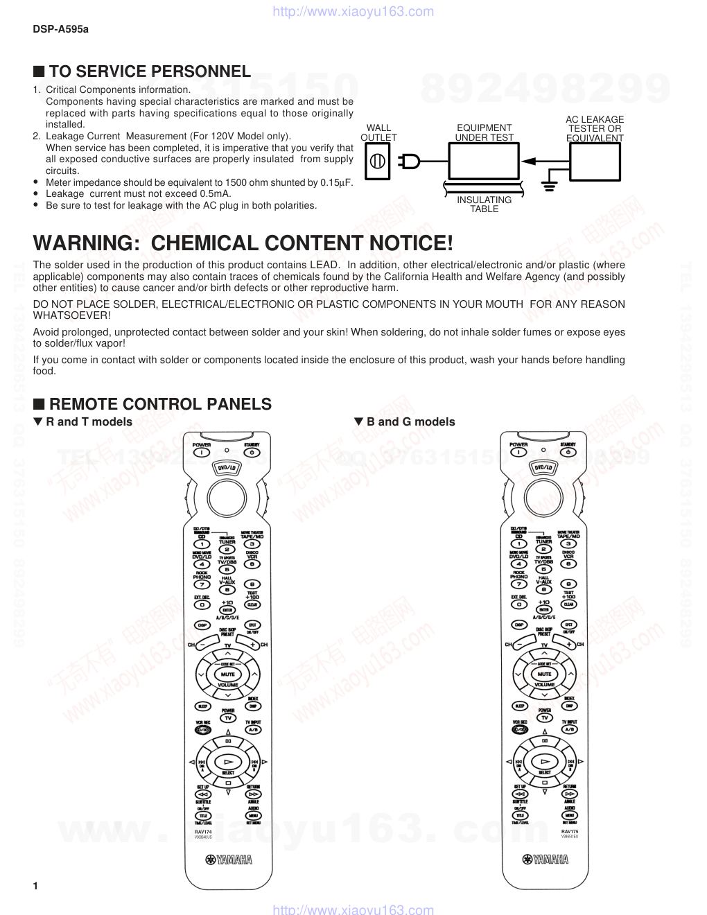
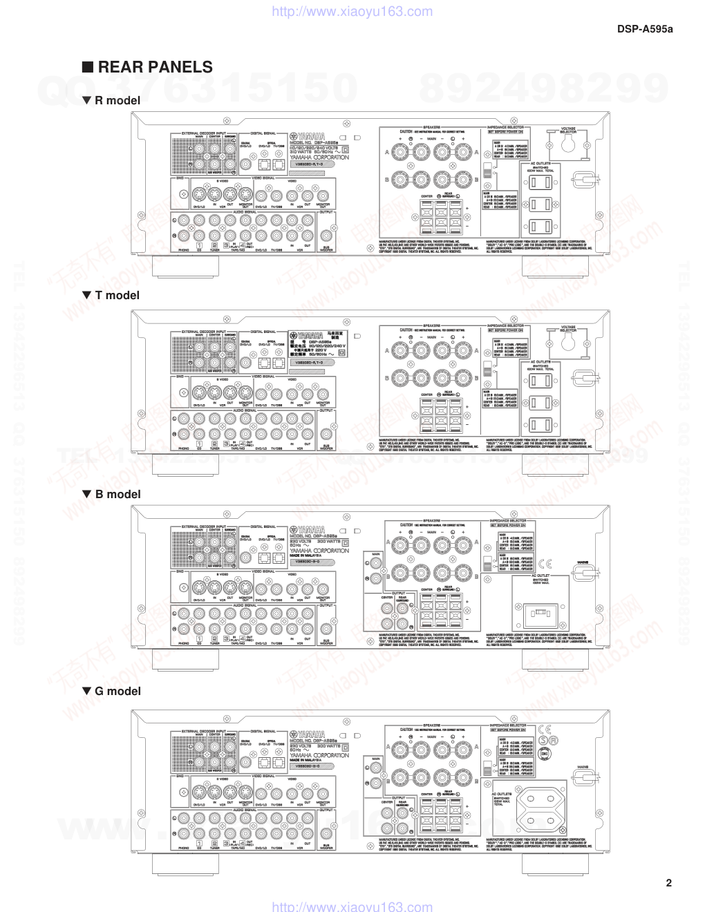
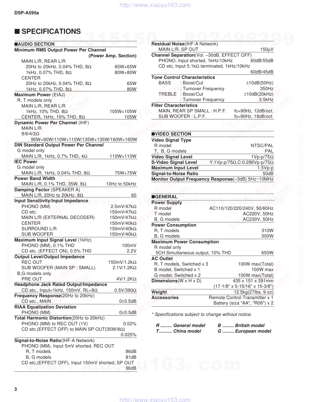
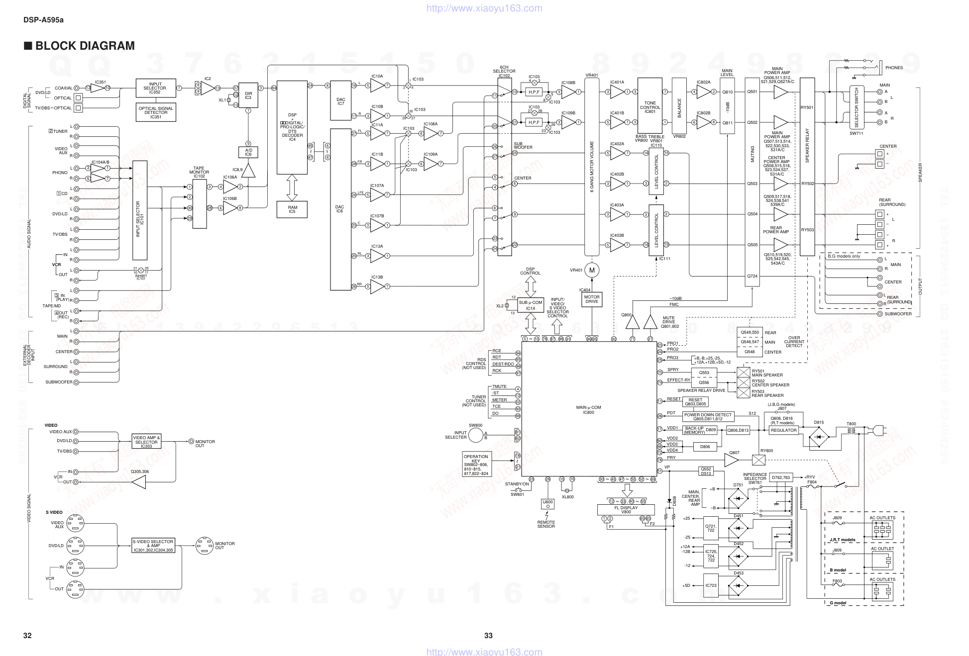
DSP-A595A电路原理图
 "DSP-A595A电路原理图-0")
 "DSP-A595A电路原理图-1")
 "DSP-A595A电路原理图-2")
 "DSP-A595A电路原理图-3")
 "DSP-A595A电路原理图-4")
 "DSP-A595A电路原理图-5")
 "DSP-A595A电路原理图-6")
 "DSP-A595A电路原理图-7")
 "DSP-A595A电路原理图-8")
 "DSP-A595A电路原理图-9")
SERVICE MANUAL IMPORTANT NOTICE This manual has been provided for the use of authorized YAMAHA Retailers and their service personnel. It has been assumed that basic service procedures inherent to the industry, and more specifically YAMAHA Products, are already known and understood by the users, and have therefore not been restated. WARNING: Failure to follow appropriate service and safety procedures when servicing this product may result in personal injury, destruction of expensive components, and failure of the product to perform as specified. For these reasons, we advise all YAMAHA product owners that any service required should be performed by an authorized YAMAHA Retailer or the appointed service representative. IMPORTANT: The presentation or sale of this manual to any individual of firm does not constitute authorization, certification or recognition of any applicable technical capabilities, or establish a principle-agent relationship of any form. The data provided is believed to be accurate and applicable to the unit(s) indicated on the cover. The research, engineering, and service departments of YAMAHA are continually striving to improve YAMAHA products. Modifications are, therefore, inevitable and specifications are subject to change without notice or obligation to retrofit. Should any discrepancy appear to exist, please contact the distributor's Service Division. WARNING: Static discharges can destroy expensive components. Discharge any static electricity your body may have accumulated by grounding yourself to the ground buss in the unit (heavy gauge black wires connect to this buss). IMPORTANT: Turn the unit OFF during disassembly and part replacement. Recheck all work before you apply power to the unit. 1 0 0 6 7 8 AV AMPLIFIER DSP-A595a TO SERVICE PERSONNEL ........................................... 1 REMOTE CONTROL PANELS ....................................... 1 REAR PANELS ............................................................... 2 SPECIFICATIONS....................................................... 3~4 INTERNAL VIEW ............................................................ 5 DISASSEMBLY PROCEDURES .................................... 5 SELF DIAGNOSIS FUNCTION ................................ 6~17 FACTORY PRESET ...................................................... 18 I CONTENTS AMP ADJUSTMENT ..................................................... 19 IC DATA .................................................................. 20~30 DISPLAY DATA ........................................................... 31 BLOCK DIAGRAM .................................................. 32~33 PRINTED CIRCUIT BOARD ................................... 34~47 SCHEMATIC DIAGRAM ......................................... 48~53 PARTS LIST ............................................................ 54~67 REMOTE CONTROL TRANSMITTER ......................... 68 www. xiaoyu163. com QQ 376315150 9 9 2 8 9 4 2 9 8 TEL 13942296513 9 9 2 8 9 4 2 9 8 0 5 1 5 1 3 6 7 3 Q Q TEL 13942296513 QQ 376315150 892498299 TEL 13942296513 QQ 376315150 892498299 http://www.xiaoyu163.com 1 DSP-A595a I TO SERVICE PERSONNEL 1. Critical Components information. Components having special characteristics are marked and must be replaced with parts having specifications equal to those originally installed. 2. Leakage Current Measurement (For 120V Model only). When service has been completed, it is imperative that you verify that all exposed conductive surfaces are properly insulated from supply circuits. • Meter impedance should be equivalent to 1500 ohm shunted by 0.15µF. • Leakage current must not exceed 0.5mA. • Be sure to test for leakage with the AC plug in both polarities. WARNING: CHEMICAL CONTENT NOTICE! The solder used in the production of this product contains LEAD. In addition, other electrical/electronic and/or plastic (where applicable) components may also contain traces of chemicals found by the California Health and Welfare Agency (and possibly other entities) to cause cancer and/or birth defects or other reproductive harm. DO NOT PLACE SOLDER, ELECTRICAL/ELECTRONIC OR PLASTIC COMPONENTS IN YOUR MOUTH FOR ANY REASON WHATSOEVER! Avoid prolonged, unprotected contact between solder and your skin! When soldering, do not inhale solder fumes or expose eyes to solder/flux vapor! If you come in contact with solder or components located inside the enclosure of this product, wash your hands before handling food. I REMOTE CONTROL PANELS M R and T models M B and G models WALL OUTLET EQUIPMENT UNDER TEST AC LEAKAGE TESTER OR EQUIVALENT INSULATING TABLE RAV174 V383640 US RAV175 V38650 EU www. xiaoyu163. com QQ 376315150 9 9 2 8 9 4 2 9 8 TEL 13942296513 9 9 2 8 9 4 2 9 8 0 5 1 5 1 3 6 7 3 Q Q TEL 13942296513 QQ 376315150 892498299 TEL 13942296513 QQ 376315150 892498299 http://www.xiaoyu163.com 2 DSP-A595a M T model M B model M G model M R model I REAR PANELS www. xiaoyu163. com QQ 376315150 9 9 2 8 9 4 2 9 8 TEL 13942296513 9 9 2 8 9 4 2 9 8 0 5 1 5 1 3 6 7 3 Q Q TEL 13942296513 QQ 376315150 892498299 TEL 13942296513 QQ 376315150 892498299 http://www.xiaoyu163.com 3 DSP-A595a I SPECIFICATIONS IAUDIO SECTION Minimum RMS Output Power Per Channel (Power Amp. Section) MAIN L/R, REAR L/R 20Hz to 20kHz, 0.04% THD, 8Ω 65W+65W 1kHz, 0.07% THD, 8Ω 80W+80W CENTER 20Hz to 20kHz, 0.04% THD, 8Ω 65W 1kHz, 0.07% THD, 8Ω 80W Maximum Power (EIAJ) R, T models only MAIN L/R, REAR L/R 1kHz, 10% THD, 8Ω 105W+105W CENTER, 1kHz, 10% THD, 8Ω 105W Dynamic Power Per Channel (IHF) MAIN L/R 8/6/4/2Ω 90W+90W/110W+110W/135W+135W/160W+160W DIN Standard Output Power Per Channel G model only MAIN L/R, 1kHz, 0.7% THD, 4Ω 110W+110W IEC Power G model only MAIN L/R, 1kHz, 0.04% THD, 8Ω 75W+75W Power Band Width MAIN L/R, 0.1% THD, 35W, 8Ω 10Hz to 50kHz Damping Factor (SPEAKER A) MAIN L/R, 20Hz to 20kHz, 8Ω 60 Input Sensitivity/Input Impedance PHONO (MM) 2.5mV/47kΩ CD etc. 150mV/47kΩ MAIN L/R (EXTERNAL DECODER) 150mV/47kΩ CENTER 150mV/40kΩ SURROUND L/R 150mV/40kΩ SUB WOOFER 150mV/40kΩ Maximum Input Signal Level (1kHz) PHONO (MM), 0.1% THD 100mV CD etc. (EFFECT ON), 0.5% THD 2.2V Output Level/Output Impedance REC OUT 150mV/1.2kΩ SUB WOOFER (MAIN SP : SMALL) 2.1V/1.2KΩ B,G models only PRE OUT 4V/1.2KΩ Headphone Jack Rated Output/Impedance CD etc., Input=1kHz, 150mV, RL=8Ω 0.5V/390Ω Frequency Response(20Hz to 20kHz) CD etc., MAIN 0±0.5dB RIAA Equalization Deviation PHONO (MM) 0±0.5dB Total Harmonic Distortion(20Hz to 20kHz) PHONO (MM) to REC OUT (1V) 0.02% CD etc.(EFFECT OFF) to MAIN SP OUT(35W/8Ω) 0.025% Signal-to-Noise Ratio(IHF-A Network) PHONO (MM), Input 5mV shorted, REC OUT R, T models 86dB B, G models 81dB CD etc,(EFFECT OFF), Input 150mV shorted, SP OUT 96dB Residual Noise(IHF-A Network) MAIN L/R, SP OUT 150µV Channel Separation(Vol. –30dB, EFFECT OFF) PHONO, Input shorted, 1kHz/10kHz 60dB/55dB CD etc, Input 5.1kΩ terminated, 1kHz/10kHz 60dB/45dB Tone Control Characteristics BASS : Boost/Cut ±10dB(50Hz) : Turnover Frequency 350Hz TREBLE : Boost/Cut ±10dB(20kHz) : Turnover Frequency 3.5kHz Filter Characteristics MAIN, REAR SP SMALL : H.P.F. fc=90Hz, 12dB/oct. SUB WOOFER : L.P.F. fc=90Hz, 18dB/oct. IVIDEO SECTION Video Signal Type R model NTSC/PAL T, B, G models PAL Video Signal Level 1Vp-p/75Ω S-Video Signal Level Y:1Vp-p/75Ω,C:0.286Vp-p/75Ω Maximum Input Level 1.5Vp-p Signal-to-Noise Ratio 50dB Monitor Output Frequency Response(–3dB) 5Hz~10MHz IGENERAL Power Supply R model AC110/120/220/240V, 50/60Hz T model AC220V, 50Hz B, G models AC230V, 50Hz Power Consumption R, T models 310W B, G models 300W Maximum Power Consumption R model only 5CH Simultaneous output, 10% THD 650W AC Outlet R, T models, Switched x 3 100W max(Total) B model, Switched x 1 100W max G model, Switched x 2 100W max(Total) Dimensions(W x H x D) 435 x 151 x 391mm (17-1/8" x 5-15/16" x 15-3/8") Weight 12.5kg(27Ibs. 9 oz) Accessories Remote Control Transmitter x 1 Battery (siza "AA", "R06") x 2 * Specifications subject to change without notice. R ......... General model B ......... British model T.......... China model G ......... European model www. xiaoyu163. com QQ 376315150 9 9 2 8 9 4 2 9 8 TEL 13942296513 9 9 2 8 9 4 2 9 8 0 5 1 5 1 3 6 7 3 Q Q TEL 13942296513 QQ 376315150 892498299 TEL 13942296513 QQ 376315150 892498299 http://www.xiaoyu163.com 4 DSP-A595a G DIMENSIONS Units: mm (inch) 21.5 (7/8") 435(17-1/8") 349.5(13-3/4") 391(15-3/8") 130(5-3/32") 151(5-15/16") 20 (13/16") 21 (27/32") WARNING Do not change the IMPEDANCE SELECTOR switch setting while the power to this unit is on, otherwise this unit may be damaged. IMPEDANCE SELECTOR Manufactured under license from Digital Theater Systems, Inc. US Pat. No. 5,451,942 and other wirld- wide patents issued and pending. "DTS", "DTS Digital Surround", are trademarks of Digital Theater Systems, Inc. Copyright 1996 Digital Theater Systems, inc. All rights reserved. www. xiaoyu163. com QQ 376315150 9 9 2 8 9 4 2 9 8 TEL 13942296513 9 9 2 8 9 4 2 9 8 0 5 1 5 1 3 6 7 3 Q Q TEL 13942296513 QQ 376315150 892498299 TEL 13942296513 QQ 376315150 892498299 http://www.xiaoyu163.com DSP-A595a 32 33 I BLOCK DIAGRAM 10 11 21 20 6CH SELECTOR IC102 26 25 27 6 5 4 8 9 7 22 23 24 OPERATION KEY SW802~806, 810~815, 817,822~824 12 4 22 93 18 21 27 50 29 47 23 11 26 90 17 46 76 51 RESET Q803,D805 POWER DOWN DETECT Q805,D811,812 BACK-UP (MEMORY) Q806,D813 REGULATOR 1 2 65 65 ~ 33 12 ~ 55 40 ~ U800 TMUTE /ST METER TCE ~ F1 F2 RESET PDT VDD1 VDD3 PRY VP STANBY/ON SW801 D808 +B –B +25 -25 F804 J809 J809 F803 Q807 RY800 S12 MAIN µ-COM IC800 REMOTE SENSOR FL DISPLAY V800 D809 , 16 15 XL2 95 94 96 97 RCE RDT DEST/RDO RCK INPUT/ VIDEO/ S VIDEO SELECTOR CONTROL Q801,802 MUTE DRIVE 14 3 14 15 2 2 15 3 5 7 IC402A 3 1 IC402B 3 1 IC403A 5 7 IC403B IC110 IC111 LEVEL CONTROL LEVEL CONTROL 6 GANG MOTOR VOLUME VR401 TONE CONTROL IC801 BASS VR800 TREBLE VR801 VR802 -10dB MAIN LEVEL Q811 BALANCE Q501 Q502 Q503 Q504 Q505 Q724 MUTING Q506,511,512, 521,529,Q527A/C Q507,513,514, 522,530,533, 531A/C Q508,515,516, 523,534,537, 531A/C Q509,517,518, 524,538,541 539A/C Q510,519,520, 525,542,545, 543A/C MAIN POWER AMP CENTER POWER AMP REAR POWER AMP RY501 RY502 RY503 L R MAIN CENTER L R SUBWOOFER REAR (SURROUND) OUTPUT SPEAKER + – L – + R + – REAR (SURROUND) CENTER A B L A B R MAIN PHONES +12A -12 74 Q556 EFFECT-RY 75 Q553 SPRY 24 PRO2 PRO1 Q548 Q546,547 Q549,550 RY503 REAR SPEAKER RY502 CENTER SPEAKER RY501 MAIN SPEAKER SPEAKER RELAY DRIVE OVER CURRENT DETECT CENTER MAIN REAR VCR PHONO CD 1 3 7 5 IC104A/B L R L R L R L R L R L R DVD/LD TV/DBS IN OUT VCR IN (PLAY) L R L R TAPE/MD L R MAIN CENTER L R SUBWOOFER SURROUND EXTERNAL DECODER INPUT AUDIO SIGNAL DIGITAL SIGNAL L R VIDEO AUX INPUT SELECTOR IC101 1 3 2 22 30 28 29 TAPE MONITOR IC102 VIDEO AUX DVD/LD TV/DBS IN OUT VCR Q305,306 VIDEO AMP & SELECTOR IC303 MONITOR OUT MONITOR OUT S-VIDEO SELECTOR & AMP IC301,302,IC304,305 IN DVD/LD OUT VIDEO AUX VCR S VIDEO T800 D751 D451 D452 MAIN, CENTER, REAR AMP RDS CONTROL (NOT USED) DSP CONTROL TUNER CONTROL (NOT USED) M IC404 IC14 VIDEO FMC Q552 D513 INPEDANCE SELECTOR SW761 D815 SPEAKER RELAY SELECTOR SWITCH SUB WOOFER CENTER 5 7 24 IC107A 3 1 23 IC107B 3 1 25 IC13A 5 7 26 IC13B LFE C RL RR 5 7 27 IC11A 3 1 28 IC11B 6 7 IC108A FL FR 6 7 IC109A DAC IC6 INHIBIT IC101 21 20 10 11 5 7 18 IC10A 3 1 17 IC10B L R 1 DAC IC7 6 8 IC106B 4 2 IC106A DSP + DIGITAL/ PRO-LOGIC/ DTS DECODER IC4 8 6 ~ 47 45 ~ 24 8 4 2 IC103 30 27 29 IC103 IC103 IC103 RAM IC5 3 1 IC108B Q810 IC8,9 OPTICAL OPTICAL TV/DBS DVD/LD 10 13 IC351 COAXIAL A/D IC6 9 1 DIR IC3 3 37 12 13 XL1 84 INPUT SELECTOR IC352 OPTICAL SIGNAL DETECTOR IC351 8 9 13 IC2 7 5 7 IC401B 3 1 IC401A 45 30 ~ , 69 52 ~ , 99 DO 81 82 A B SW800 INPUT SELECTER 87 78 10 12 13 5 ~ 91 88 , , , 77 Q800 –10dB VR401 MOTOR DRIVE SUB µ-COM 85 92 86 H,P,F 3 4 5 8 IC103 IC103 MAIN POWER AMP SW711 23 +B,-B,+25,-25, +12A,+12B,+5D,-12 25 PRO3 72 VDD2 VDD4 D806 Q721, 722 +5D -12B D453 IC725, 724, 722 IC723 D762,763 +RYV 5 7 3 1 4 2 IC802A 6 8 IC802B 3 1 IC109B H,P,F 26 27 26 23 IC103 IC103 VIDEO SIGNAL 1 TUNER L R 2 3 OUT (REC) 4 Q808, D816 (R,T models) (J,B,G models) J807 B.G models only XL800 AC OUTLETS AC OUTLETS AC OUTLET G model B model J,R,T models w w w . x i a o y u 1 6 3 . c o m Q Q 3 7 6 3 1 5 1 5 0 9 9 2 8 9 4 2 9 8 T E L 1 3 9 4 2 2 9 6 5 1 3 9 9 2 8 9 4 2 9 8 0 5 1 5 1 3 6 7 3 Q Q TEL 13942296513 QQ 376315150 892498299 TEL 13942296513 QQ 376315150 892498299 http://www.xiaoyu163.com 6 DSP-A595a I SELF DIAGNOSIS FUNCTION 1. PURPOSE AND OPERATION The DSP-A595a has a Self Diagnosis Function to locate a faulty part, if any, by inspecting and taking measurements. There are 11 main items in the diagnostic menu and some of them have sub-menu items as listed below. No. 1 2 3 4 5 6 7 8 9 10 11 SUB MENU 1. MAIN BYPASS 2. DSP 0dB 1. YSS918–SRAM 2. YSS918 3. DSP FULL BIT 1. STATUS (BINARY FORM) 1. CENTER LARGE 2. EFFECT OFF 1. MAIN : SMALL 0dB 2. MAIN : LARGE 0dB 3. MAIN : LARGE –10dB 4. LFE/BASS : MAIN CENTER : NONE 5. LFE/BASS : MAIN 6. LFE/BASS : SWFR 7. CENTER : NONE 8. CENTER : SMALL REAR : SMALL 9. FRONT MIX 1. EFFECT OFF 2. VFD DISP OFF 3. VFD DISP ALL 4. CHECKED PATTERN 5. RELEASE DATE 1. ALL 2. MAIN L 3. CENTER 4. MAIN R 5. REAR R 6. REAR L 7. LFE 1. INHIBIT(Inhibit Memory Init) 2. RESERVED (Init. Memory) 1. – – – 2. KEY 3. TUNING SIGNAL 5. PS PROTECTION 1. DSP CPU STATUS 2. CHANNEL STATUS 3. VERSION INFORMATION 4. CHECK SUM 5. BSI0 (AC3/DTS) 6. BSI1 7. BSI2 8. BSI3 9. BSI4 10. BSI5 1. MAIN MC CHECK SUM 2. SUB MC CHECK SUM 3. MAIN M.C. VERSION 4. SUB M.C. VERSION 5. PORT INFORMATION 6. EXIT MAIN MENU ANALOG THROUGH DSP THROUGH AC–3/DTS THROUGH PRO LOGIC SPEAKERS SET EFFECT OFF /DISPLAY CHECK MANUAL TEST FACTORY PRESET AD DATA CHECK STATUS VERSION CHECK /DSP CPU SUM /EXIT REMOTE CONTROL CODE (KEY) 7A–88 ("1" [DSP mode]) – – – 7A–89 ("2" [DSP mode]) – – – – – – – – – 7A–8A ("3" [DSP mode]) – – – 7A–8B ("4" [DSP mode]) 7A–8C ("5" [DSP mode]) 7A–8D ("6" [DSP mode]) 7A–8E ("7" [DSP mode]) 7A–8F ("8" [DSP mode]) 7A–90 ("9" [DSP mode]) 7A–91 ("0" [DSP mode]) – – – 7A–12 ("ENTER" [DSP mode]) – – – – – – – – – – – – – – – – – – – – – – – – – – – – – – – – – – – – – – – – – – – – – – – – – – – 4. DC PROTECTION – – – – – – – – – – – – – – – – – – – – – – – – – – – – – – – – – – – – – – – – – – www. xiaoyu163. com QQ 376315150 9 9 2 8 9 4 2 9 8 TEL 13942296513 9 9 2 8 9 4 2 9 8 0 5 1 5 1 3 6 7 3 Q Q TEL 13942296513 QQ 376315150 892498299 TEL 13942296513 QQ 376315150 892498299 http://www.xiaoyu163.com 7 DSP-A595a STANDBY/ON + – SET MENU TIME/ LEVEL INPUT MODE 1. 2. 3. 4. 5. 6. 7. EFFECT LEVEL : MUTING : OFF INPUT (VIDEO) : DVD/LD (DVD/LD) CENTER SPEAKER : LARGE REAR SPEAKER : LARGE MAIN SPEAKER : LARGE LFE/BASS OUT : SWFR CHANNEL CENTER R SUR L SUR SWFR LEVEL (dB) 0 0 0 0 C. Start-up display The protection function information appears on the front panel display of the main unit. 2. BEGINNING AND CANCELLATION (1) STARTING UP THE FUNCTION AND THE DISPLAY After starting up, menu No. 1 is selected. A. How to start diagnostic program Using the front panel keys of the main unit. and then press the "STANDBY/ON" key (Step 2). Plug in the AC power cord , and, with Power OFF, hold down the "INPUT MODE" and "+" keys simultaneously (Step 1), Submenu No. 1 of the Diagnosis Main Menu No. 1 will start. B. Settings for start-up of diagnostic program The settings used when starting the diagnostic program are as follows. "+" key "STANDBY/ON" key "INPUT MODE" key FRONT PANEL Step2. Press the "STANDBY/ON" key Step1. Hold down the "INPUT MODE" and "+" key simultaneously. www. xiaoyu163. com QQ 376315150 9 9 2 8 9 4 2 9 8 TEL 13942296513 9 9 2 8 9 4 2 9 8 0 5 1 5 1 3 6 7 3 Q Q TEL 13942296513 QQ 376315150 892498299 TEL 13942296513 QQ 376315150 892498299 http://www.xiaoyu163.com 8 DSP-A595a G History of protection function Each case of the history of the protection function is displayed as shown below. Appears when the protection function has not been activated. Appears when the current protection function has been activated. When power is turned on in an abnormal status, the power relay will come on, protection will operate immediately, and power will turn off. Appears when the power protection function has been activated. For the % value, the voltage at that point is shown by 5V/100%. When power is turned on in an abnormal status, power will turn off after half a second. Appears when the power amp DC protection function has been activated. For the % value, the voltage at that point is shown by 5V/100%. When power is turned on in an abnormal status, power will turn off after two seconds. G FL display at start-up of diagnostic program When the diagnostic program has started, the history (*2) of the protection function (*1) is displayed. If the protection function has been activated in the past, the type and voltage value are displayed. After a few seconds the diagnosis function menu will appear. (*1) If a faulty condition is detected such as excessive current, a bad power supply or excessive amplifier DC offset, the Power will be switched OFF automatically. (*2) The protection records will be cleared when "RESERVED" is selected in diagnosis menu No. 8 and FACTORY PRESET is engaged. 1 DVD/LD NO PROTECT 1 DVD/LD I PROTECT 1 DVD/LD PS : 21% 1 DVD/LD DC : 19% (2) EXITING METHOD The diagnosis function can be exited by any of the following procedures. Take care with the setting of backup memory initialization menu (diagnosis No. 8) when releasing the diagnosis function: 1. Select diagnosis menu No. 11/submenu No. 6 "EXIT". 2. Press the "STANDBY/ON" key on the main unit or "STANDBY" key on the remote control to turn power off. www. xiaoyu163. com QQ 376315150 9 9 2 8 9 4 2 9 8 TEL 13942296513 9 9 2 8 9 4 2 9 8 0 5 1 5 1 3 6 7 3 Q Q TEL 13942296513 QQ 376315150 892498299 TEL 13942296513 QQ 376315150 892498299 http://www.xiaoyu163.com 9 DSP-A595a G Selection by using the remote control unit The remote control codes in the menu list (see right column on page 6) correspond to the DSP program test and effect keys. See the figure on the right. 3. OPERATION AND DISPLAY WHEN STARTING DIAGNOSIS FUNCTION (1) Selection of diagnostic menu The diagnostic menu and the sub-menu can be selected by using the front panel keys of the main unit or the remote control unit. (2) Other functions available while diagnosis function is active Listed below are the other functions available while the diagnosis function is active. • Selecting input source (Tape monitor/Ext. decoder) • Adjusting effect level (Center, Rear, Subwoofer) • Adjusting master volume • Muting on/off • Power on/off (3) Diagnosis default status When not otherwise specified, default settings and values in each menu are as follows: • All “SPEAKERS” : LARGE • ALL electronic VRs : 0dB • DYNAMIC RANGE : MAX • LFE LEVEL : 0dB (DOLBY DIGITAL, DTS) • CENTER DELAY : 0ms G Selection by using the front panel keys The main menu can be changed cyclically by using the "TV SPORTS" and "DISCO" keys, and the submenu, by using the "ROCK CONCERT" and "CONCERT HALL" keys. The "DISCO" or "CONCERT HALL" key will increase the main or submenu number. TV SPORTS DISCO ROCK CONCERT CONCERT HALL FRONT PANEL Main menu Forward Reverse Sub menu Forward Reverse 7A D S P www. xiaoyu163. com QQ 376315150 9 9 2 8 9 4 2 9 8 TEL 13942296513 9 9 2 8 9 4 2 9 8 0 5 1 5 1 3 6 7 3 Q Q TEL 13942296513 QQ 376315150 892498299 TEL 13942296513 QQ 376315150 892498299 http://www.xiaoyu163.com 10 DSP-A595a 4. CONTENTS OF DIAGNOSIS FUNCTION This section describes the contents of the self diagnosis function in detail. No.1 ANALOG THROUGH The input is fixed to analog (A/D). There are two submenus. 1. MAIN BYPASS The MAIN L/R signals bypass the analog circuits to be output. For CENTER/LFE, FRONT L/R and REAR L/R, the MAIN L/R signals via the DSP are output without being processed (through). (Remote control code 7A-88: "1" key [DSP mode]) : This shows that the device is not operating. 2. DSP 0dB MAIN L/R, CENTER/LFE, FRONT L/R and REAR L/R pass through the DSP without being processed. : This shows that the device is not operating. DIR2 CODEC.DA AK4526A YM3436 CODEC.AD AC3D2av(YSS918) AK4526A DECODER DA AK4320 1M SRAM DSP ANALOG IN L/R L/R FRONT R REAR L REAR R CENTER SUBWOOFER L/R L/R L/R DIGITAL IN FRONT L MAIN R MAIN L DIR2 CODEC.DA AK4526A YM3436 CODEC.AD AC3D2av(YSS918) AK4526A DECODER DA AK4320 1M SRAM DSP ANALOG IN L/R L/R FRONT R REAR L REAR R CENTER SUBWOOFER L/R L/R L/R DIGITAL IN FRONT L MAIN R MAIN L 1 DVD/LD DSP 0DB 1 DVD/LD MAIN BYPAS • INPUT : DVD/LD (Analog signal) (Lch and Rch, 1KHz, –20dBV) • OUTPUT : SPEAKERS MAIN L : 23.8 dBV REAR L : 23.7 dBV MAIN R : 23.8 dBV REAR R : 23.7 dBV CENTER: 23.7 dBV • INPUT : DVD/LD (Analog signal) (Lch and Rch, 1KHz, –20dBV) • OUTPUT : SPEAKERS MAIN L : 23.7 dBV REAR L : 23.6 dBV MAIN R : 23.7 dBV REAR R : 23.6 dBV CENTER: 23.6 dBV www. xiaoyu163. com QQ 376315150 9 9 2 8 9 4 2 9 8 TEL 13942296513 9 9 2 8 9 4 2 9 8 0 5 1 5 1 3 6 7 3 Q Q TEL 13942296513 QQ 376315150 892498299 TEL 13942296513 QQ 376315150 892498299 http://www.xiaoyu163.com 11 DSP-A595a No.2 DSP THROUGH The input is automatically discriminated by signal detection and switched with priorities AC-3 (DOLBY DIGITAL)>DTS Digital Surround>Audio>analog. There are the following three submenus. 1. YSS918-SRAM MAIN L/R are input to the DSP via AC3D2av, pass through SRAM, and are then output to all channels without being processed. (Remote control code 7A-89: "2" key [DSP mode]) 2. YSS918 MAIN L/R are input to the DSP via AC3D2av, and then output to all channels without being processed. 3. DSP FULL BIT MAIN L/R are input to the DSP via AC3D2av, and then output to all channels without being processed. The head margin is disabled, and DSP outputs digital full-bit signals. Same as the above menu, except that the digital data is output to DA with full bits. DIR2 CODEC.DA AK4526A YM3436 CODEC.AD AC3D2av(YSS918) AK4526A DECODER DA AK4320 1M SRAM DSP ANALOG IN L/R REAR L REAR R CENTER SUBWOOFER L/R DIGITAL IN FRONT R FRONT L MAIN R MAIN L L/R L/R DIR2 CODEC.DA AK4526A YM3436 CODEC.AD AC3D2av(YSS918) AK4526A DECODER DA AK4320 1M SRAM DSP ANALOG IN L/R FRONT R REAR L REAR R CENTER SUBWOOFER L/R L/R L/R L/R DIGITAL IN FRONT L MAIN R MAIN L : This shows that the device is not operating. 2 DVD/LD YSS918SRAM 2 DVD/LD YSS918 2 DVD/LD DSP FULL L/R L/R L/R • INPUT : DVD/LD (Analog signal) (Lch and Rch, 1KHz, –20dBV) • OUTPUT : SPEAKERS MAIN L : 23.7 dBV REAR L : 23.5 dBV MAIN R : 23.7 dBV REAR R : 23.5 dBV CENTER: 23.6 dBV • INPUT : DVD/LD (Analog signal) (Lch and Rch, 1KHz, –20dBV) • OUTPUT : SPEAKERS MAIN L : 23.8 dBV REAR L : 23.8 dBV MAIN R : 23.8 dBV REAR R : 23.8 dBV CENTER: 23.8 dBV • INPUT : DVD/LD (Analog signal) (Lch and Rch, 1KHz, –20dBV) • OUTPUT : SPEAKERS MAIN L : 13.8 dBV REAR L : 22.8 dBV MAIN R : 13.8 dBV REAR R : 22.8 dBV CENTER: 16.8 dBV www. xiaoyu163. com QQ 376315150 9 9 2 8 9 4 2 9 8 TEL 13942296513 9 9 2 8 9 4 2 9 8 0 5 1 5 1 3 6 7 3 Q Q TEL 13942296513 QQ 376315150 892498299 TEL 13942296513 QQ 376315150 892498299 http://www.xiaoyu163.com 12 DSP-A595a No.3 AC-3/DTS THROUGH The input is digital signal only. AC-3 (DOLBY DIGITAL) or DTS Digital Surround decoding operation is executed, according to the input source. 1. STATUS(BINARY FORM) AC-3 (DOLBY DIGITAL) decoded signals are output to each channel via AC3D2av. AC-3 Status Info. : bit 7 6 5 4 3 2 1 0 (Invalid in DTS) 1 0 0 0 0 0 0 0 IEC958 digital data bit IEC958 commercial-use device bit IEC958 digital format error Demodulator muting (without RF signal) 1 for audio other than PCM linear audio 1 during red DTS lock 1 during DTS decode OK 1 during AC-3 decode OK No.4 PRO LOGIC The input is automatically discriminated by PCM Audio>analog. DTS Digital Surround is disabled. The submenu is switched between PRO LOGIC (AUTO BALANCE OFF) and EFFECT OFF. 1. CENTER LARGE The input is automatically detected whether it is PCM Audio or analog. With analog, PCM Audio or AC-3 (DOLBY DI- GITAL) 2/0 input, the L, R, C and S signals are PRO LOGIC decoded and output. With AC-3 (DOLBY DIGITAL) other than 2/0, PRO LOGIC does not operate, and AC-3 (DOLBY DIGITAL) playback is executed. (Remote control code 7A-8A: "3" key [DSP mode]) 2. EFFECT OFF MAIN L/R are bypassed and output. DIR2 CODEC.DA AK4526A YM3436 CODEC.AD AC3D2av(YSS918) AK4526A DECODER DOLBY DIGITAL or PRO LOGIC or DTS or DTS DA AK4320 1M SRAM DSP ANALOG IN REAR L REAR R CENTER SUBWOOFER L/R DIGITAL IN MAIN R MAIN L LS/RS LS/RS C/LFE C/LFE DIR2 CODEC.DA AK4526A YM3436 CODEC.AD AC3D2av(YSS918) AK4526A DECODER DOLBY DIGITAL or PRO LOGIC DA AK4320 1M SRAM DSP ANALOG IN C S C S REAR L REAR R CENTER L/R DIGITAL IN MAIN R MAIN L : This shows that the device is not operating. 4 DVD/LD P. LGC C:L 4 DVD/LD EFFECT OFF 3 DVD/LD 3T00000001 • INPUT : DVD/LD (Analog signal) (Lch and Rch, or Lch only, 1KHz, –20dBV) • OUTPUT : SPEAKERS (INPUT : Lch and Rch ) (INPUT : Lch only) MAIN L : –15.4 dBV REAR L : 23.8 dBV MAIN R : –14.2 dBV REAR R : –25.0 dBV CENTER: 26.6 dBV CENTER : –12.5 dBV REAR L : –6.0 dBV REAR L : –6.0 dBV REAR R : –6.5 dBV REAR R : –6.2 dBV bit 0 bit 7 www. xiaoyu163. com QQ 376315150 9 9 2 8 9 4 2 9 8 TEL 13942296513 9 9 2 8 9 4 2 9 8 0 5 1 5 1 3 6 7 3 Q Q TEL 13942296513 QQ 376315150 892498299 TEL 13942296513 QQ 376315150 892498299 http://www.xiaoyu163.com 13 DSP-A595a No.5 SPEAKERS SET The input is automatically discriminated by AC-3(DOLBY DIGITAL)>DTS Digital Surround>PCM Audio>analog. There are the following 9 submenu items: The signal from the DSP block is normally in the effect off status for menu items 1-4. For other menu items, the same signal as in 2. DSP THROUGH: YSS918 menu is output. SUB MENU CENTER SP OUTPUT LFE/BASS MAIN LEVEL MAIN SP REAR SP REMOTE CODE 1 MAIN:S 0DB 7A-8B LARGE LARGE SMALL 0dB SWFR MAIN L/R 2 MAIN:L 0DB 7A-8C LARGE LARGE LARGE 0dB SWFR MAIN L/R 3 MAIN:L -10 7A-8D LARGE LARGE LARGE -10dB SWFR MAIN L/R 4 B:MAIN C:N 7A-8E NONE LARGE LARGE 0dB MAIN MAIN L/R 5 LFE/B:MAIN 7A-8F LARGE LARGE LARGE 0dB MAIN LFE -> L/R 6 LFE/B:SWFR 7A-90 LARGE LARGE LARGE 0dB SWFR LFE -> SWFR 7 C:NONE 7A-91 NONE LARGE LARGE 0dB SWFR CENTER -> L/R 8 C:S REAR:S SMALL SMALL LARGE 0dB SWFR CENTER/REAR 9 FRONT MIX 7A-12 LARGE LARGE LARGE 0dB SWFR FRONT -> L/R SUB MENU PURPOSE 1 MAIN:S 0DB Verification of the High and low pass filter response and gain in the bass redirection mode. 2 MAIN:L 0DB Reference of the sub menu No. 1 and 2. 3 MAIN:L -10 Verification of the effect in the main level function. 4 B:MAIN C:N Verification of the mixing circuit effect to the main channel. 5 LFE/B:MAIN Verification of the bass mix gain. 6 LFE/B:SWFR Verification of the LFE maximum output. 7 C:NONE Verification of the center mix gain. 8 C:S REAR:S Verification of the high and low pass filter response and gain in the bass redirection mode. 9 FRONT MIX Verification of the front mix gain. LARGE: Mode in which speakers with high bass-sound playback capability (large unit) are used. Full frequency band widths is output. SMALL : Mode in which speakers with low bass-sound playback capability (small unit) are used. Frequncies below 90 Hz are mixed with the channel specified by LFE/BASS. NONE: Mode in which center speaker is not used. The center audio signal is reduced by 3 dB and mixed into MAIN L/R. LFE/B: MAIN : Mode in which subwoofer speaker is not used. The subwoofer audio signal is reduced by 4.5 dB and mixed into MAIN L/R. But because of the phase difference, the MAIN L/R output is not simply summed. The analog switches in each submenu are set as follows: Purpose of the submenu as follows: 5 DVD/LD MAIN:S 0DB 5 DVD/LD B:MAIN C:N 5 DVD/LD C:NONE 5 DVD/LD MAIN:L 0DB 5 DVD/LD LFE/B:MAIN 5 DVD/LD C:S REAR:S 5 DVD/LD MAIN:L —10 5 DVD/LD LFE/B:SWFR 5 DVD/LD FRONT MIX www. xiaoyu163. com QQ 376315150 9 9 2 8 9 4 2 9 8 TEL 13942296513 9 9 2 8 9 4 2 9 8 0 5 1 5 1 3 6 7 3 Q Q TEL 13942296513 QQ 376315150 892498299 TEL 13942296513 QQ 376315150 892498299 http://www.xiaoyu163.com 14 DSP-A595a No.6 DISPLAY CHECK Check program for FL display. The display status will change as follows with submenu operation. The signal is processed with EFFECT OFF. All segments are turned on and off to detect defects in the FL driver and FL display segments. Then the FL driver operation is checked by the dimmer control. Finally, all segments are turned on and off alternately (in lattice form), to check for a short-circuit between adjacent segments. No.7 MANUAL TEST The noise generator built into the DSP outputs test noise from the channel specified by the submenu. No.8 FACTORY PRESET The initialization of the back-up RAM, which contains effect level, DSP program, set menu contents, etc. is reserved or inhibited. The Signal is processed with EFFECT OFF. 1. INHIBIT: Inhibits initialization of the back-up RAM. Specify this option protect user set Values. 2. RESERVED: Reserve to initialization of the back-up RAM. (The RAM is actually initialized when power is turned on next time.) Specify this option at the factory preset or to reset the RAM. For the contents of the initialization, see page 18. The protection data is also reset. 6 DVD/LD DISP CHECK 6 DVD/LD 9902161625 7 DVD/LD TEST ALL 7 DVD/LD TEST MAINR 7 DVD/LD TEST LFE 8 DVD/LD PRESET INH 8 DVD/LD PRESET RES 7 DVD/LD TEST MAINL 7 DVD/LD TEST REARR 7 DVD/LD TEST CNTR 7 DVD/LD TEST REARL Initial display All segments turn off All segments turn on Segments light in lattice form Release date display www. xiaoyu163. com QQ 376315150 9 9 2 8 9 4 2 9 8 TEL 13942296513 9 9 2 8 9 4 2 9 8 0 5 1 5 1 3 6 7 3 Q Q TEL 13942296513 QQ 376315150 892498299 TEL 13942296513 QQ 376315150 892498299 http://www.xiaoyu163.com 15 DSP-A595a No.9 AD DATA CHECK The A/D conversion values of the main CPU which detects key scan, protection, etc. are displayed in % (100%: 5V). All signal processing before this menu is executed will be held. The keys on the main unit cannot be operated to detect the values of all keys in the K1/K2/K3/K4 and SI. Operating the "CONCERT HALL" key and turning the rotary encoder (input selector on the main unit) will switch the submenu. Press the "CONCERT HALL "key. K1/K2/K3/K4: Panel key on main unit See Table 1. Turning the rotary encoder. SI: Tuner signal level Turning the rotary encoder. DC: DC protection value (normal value: 1-13) Press the "CONCERT HALL"key. PS: Power voltage protection value Table 1 (normal value: 28-54) 1.If K1/K2/K3/K4 are more than ±4% from the reference values, normal operation will not be executed. 2.If DC and PS are outside the normal values, the protection function will operate and power will turn off. Cautions: K1 K2 K3 K4 9 DVD/LD AD DATACHK 9 DVD/LD K99999999 9 DVD/LD SI 0 9 DVD/LD DC 7 9 DVD/LD PS 40 Press the "CONCERT HALL"key. AD Value 0 11 23 36 51 67 84 TAPE/MD MON /EXT. DECODER ROCK CONCERT EFFECT CONCERT HALL /DTS SURROUND SET MENU ENHANCED INPUT MODE MOVIE THEATER – + MONO MOVIE TV SPORTS DISCO K1 K2 K3 K4 TIME/ LEVEL www. xiaoyu163. com QQ 376315150 9 9 2 8 9 4 2 9 8 TEL 13942296513 9 9 2 8 9 4 2 9 8 0 5 1 5 1 3 6 7 3 Q Q TEL 13942296513 QQ 376315150 892498299 TEL 13942296513 QQ 376315150 892498299 http://www.xiaoyu163.com 16 DSP-A595a No.10 STATUS FROM DSP MICOM The status data from the DSP microprocessor is sequentially displayed in a hexadecimal number. All signal processing before this menu is executed will be held. [STATUS 0] <1st Byte> acmod: If it is 1000B or more with DTS 7.1 signal, the DSP block will be muted. <2nd Byte> [Note] <3rd Byte> <4th Byte> Always “00” [STATUS 1] IEC958 channel status bits 00-31 available from DIR2 <1st-byte> bits 00-07 <2nd-byte> bits 08-15 <3rd-byte> bits 16-23 <4th-byte> bits 24-31 [STATUS 2] 4-byte ASCII code of sub CPU version data [STATUS 3] Displays the check sum of sub microprocessor program area with ASCII 4 bytes in a hexadecimal number. [STATUS 4] Displays the bit stream information contained in AC-3(DOLBY DIGITAL)/DTS Digital Surround signal from the first byte. [STATUS 5-9] Displays the bit stream information contained in AC-3(DOLBY DIGITAL) signal from the first byte. bit7 AC3 KARAOKE bit3 On-board write mode bit6 DIR2 LOCKN bit2 The number of digital inputs is 2 (equivalent to 595) bit5 DIR2 ERR bit1 DSP is AC3D2 (DTS present) bit4 AC3D MUTE bit0 RF DEM present 10 DVD/LD 0 00000000 10 DVD/LD 3 00000000 10 DVD/LD 6 00000000 10 DVD/LD 1 00000000 10 DVD/LD 4 00000000 10 DVD/LD 7 00000000 10 DVD/LD 2 00000000 10 DVD/LD 5 00000000 10 DVD/LD 8 00000000 10 DVD/LD 9 00000000 bit7 AC-3 decode OK bit3 Demodulator muting (without RF signal) bit6 DTS decode OK bit2 IEC958 digital format error bit5 Red DTS record (Flashes and lights) bit1 IEC958 commercial use device bit bit4 1 for audio other than PCM linear audio bit0 IEC958 digital data bit bit7 Mute request bit3 acmod 0000B:1+1 0001B:1/0 0010B:2/0 0011B:3/0 0100B:2/1 0101B:3/1 0110B:2/2 0111B:3/2 1000B:7.1 bit6 fs bit2 bit5 000B:Analog 001B:32kHz 010B:44.1kHz 011B:48kHz Others:Don't care bit1 bit4 bit0 IEC958: Standard to identify the PCM bit stream signal. Digital format error refers to a digital signal with the sampling frequency undefined (neither 44.1k, 32k nor 48k). Since the operation of each device cannot be assured at fs outside specifications, the sub-microprocessor handles this status as the forced analog mode (ignored even if decoding is OK from the detection terminal level), and selects the signal from the analog input terminal. Since the sub-microprocessor transmits 000B (analog) for STATUS#0 bits 4-6 to the main microprocessor, the main microprocessor visually operates in the same way as with digital unlocking. Indicate bit 3 2 1 0 7 6 5 4 0 0 0 0 0 1 0 0 0 1 2 0 0 1 0 3 0 0 1 1 4 0 1 0 0 5 0 1 0 1 6 0 1 1 0 7 0 1 1 1 8 1 0 0 0 9 1 0 0 1 A 1 0 1 0 B 1 0 1 1 C 1 1 0 0 D 1 1 0 1 E 1 1 1 0 F 1 1 1 1 bit 7 6 5 4 3 2 1 0 Indicate 0 0 1st 2nd 3rd 4th STATUS www. xiaoyu163. com QQ 376315150 9 9 2 8 9 4 2 9 8 TEL 13942296513 9 9 2 8 9 4 2 9 8 0 5 1 5 1 3 6 7 3 Q Q TEL 13942296513 QQ 376315150 892498299 TEL 13942296513 QQ 376315150 892498299 http://www.xiaoyu163.com 17 DSP-A595a 11 DVD/LD S-VER:Z08B Main microprocessor check sum DSP microprocessor check sum Main microprocessor version DSP microprocessor version One suffix letter is for compatibility of communications between the main and DSP microprocessors. * Use microprocessors with the same suffix. EXIT 81 Tuner Mode V2 (Port 96) 0 *1 1 *2 0 *3 1 *4 Tuner Mode V1 (Port 95) 0 0 1 1 *1 AM:531–1611kHz/9kHz FM: 76.0–90.0MHz/100kHz (J model) *2 AM:530–1710kHz/10kHz FM: 87.5–107.9MHz/200kHz (U, C models) *3 AM:531–1611kHz/9kHz FM: 87.5–108.0MHz/50kHz (R, T, A, B, G, L models) *4 AM: 530-1710kHz/10kHz FM:87.5-108.0 MHz/100kHz (R, T models) 82 bit 7 6 5 4 3 2 1 0 1 0 0 0 0 0 0 0 Always absent (0) Always absent (0) Tuner Mode V1 (81) Tuner Mode V2 (81) Always absent (0) Always absent (0) Model Type RDS (82) Model Type DSP-A (82) No.11 CPU VERSION/CHECK SUM/PORT INFO/EXIT DIAG The check sum, version and port setting of main CPU/DSP CPU are displayed. The signal is EFFECT OFF. Operating the submenu will finish self-diagnosis, and ordinary operation mode will be restored. The suffix letter ("B" in the following) of version indication is for compatibility of communications between the main and DSP microprocessors. Combining microprocessors with different suffixes will make normal operation impossible. 11 DVD/LD M-SM:XXXXX 11 DVD/LD S-SM:XXXXX 11 DVD/LD M-VER:Z04B 11 DVD/LD P:00000000 Model Type DSP-A(Port 83) 1 DSP-A595a 0 RX-V595aRDS 0 RX-V595a HTR-5150 0 1 0 Model Type RDS(Port 70) Hi=1, Low=0 Hi=1, Low=0 www. xiaoyu163. com QQ 376315150 9 9 2 8 9 4 2 9 8 TEL 13942296513 9 9 2 8 9 4 2 9 8 0 5 1 5 1 3 6 7 3 Q Q TEL 13942296513 QQ 376315150 892498299 TEL 13942296513 QQ 376315150 892498299 http://www.xiaoyu163.com 18 DSP-A595a I FACTORY PRESET All of the system settings are initially set from the factory as follows. G INPUT (VIDEO) DVD/LD (DVD/LD) G EFFECT LEVEL EFFECT CHANNEL PRESET VALUE CENTER 0 dB RIGHT SURROUND 0 dB LEFT SURROUND 0 dB SUBWOOFER 0 dB G DSP PROGRAM INPUT DSP PROGRAM DELAY PRESET VALUE V-AUX DOLBY PRO LOGIC 20ms VCR PRO LOGIC ENHANCED 20ms VDV/LD 70mm MOVIE THEATER 20ms DIGITAL/DTS MOVIE THEATER 16ms TV/DBS TV SPORTS 9ms TAPE/MD ROCK CONCERT 49ms TUNER DISCO 40ms CD ROCK CONCERT 16ms PHONO CONCERT HALL 44ms G SET MENU No. SET MENU PRESET VALUE 8. DTS LFE LEVEL [DTS LFE] 0 dB 7. DYNAMIC RANGE [D. RNG] MAX 6. DOLBY DIGITAL LFE LEVEL [D. D. LFE] 0 dB 1. CENTER SPEAKER [CNTR>] LARGE 2. REAR SPEAKER [REAR>] LARGE 3. MAIN SPEAKER [MAIN>] LARGE 4. LFE/BASS OUT [BASS>] SW (SUBWOOFER) 5. MAIN LEVEL [M. LVL>] NRML (NORMAL) 9. CENTER DELAY [C. DELAY] 0 ms 11. 10. INPUT MODE (TV/DBS) [INPUT] AUTO MEMORY GUARD [GUARD] OFF www. xiaoyu163. com QQ 376315150 9 9 2 8 9 4 2 9 8 TEL 13942296513 9 9 2 8 9 4 2 9 8 0 5 1 5 1 3 6 7 3 Q Q TEL 13942296513 QQ 376315150 892498299 TEL 13942296513 QQ 376315150 892498299 http://www.xiaoyu163.com 19 DSP-A595a Confirmation of Idling Current of Main Amplifier • Right after power is turned on, confirm that the voltage across the terminals of R688(Main Lch),R690(Main Rch), R692(Center), R694(Rear Lch), R696(Rear Rch) are between 0.1mVand 5.0mV. • If it exceeds 5.0mV, open (cut off) R571 (Main Lch), R577 (Main Rch), R589 (Center), R595 (Rear Lch), R583 (Rear Rch) and reconfirm the voltage again. • Confirm that the voltage is 0.25mV ~ 15.0mV after 60 minutes. I AMP ADJUSTMENT Note) • If R571, R577, R589, R595 and R583 have already been cut off and idling current does not flow, reconnect R571, R577, R589, R595 and R583. • Q521 ~ Q525 are transistors for temperature correction. Apply silicone grease to contact surface with the heat sink. R571(Lch) R577(Rch) R589(Cch) R595(RLch) R583(RRch) R583 R692 R595 R589 MAIN (1) MAIN (7) Q523 Q525 Q524 Q522 Q521 R696 R694 R690 R688 R577 R571 Front Panel 0.1mV ~ 5.0mV (DC) R688(Lch) R690(Rch) R692(Cch) R694(RLch) R696(RRch) Cut off www. xiaoyu163. com QQ 376315150 9 9 2 8 9 4 2 9 8 TEL 13942296513 9 9 2 8 9 4 2 9 8 0 5 1 5 1 3 6 7 3 Q Q TEL 13942296513 QQ 376315150 892498299 TEL 13942296513 QQ 376315150 892498299 http://www.xiaoyu163.com 5 DSP-A595a I DISASSEMBLY PROCEDURES (Remove parts in disassembly order as numbered.) 1. Removal of Top Cover Remove 4 screws (1) and 4 screws (2) in Fig. 1. 2. Removal of Front Panel a. Remove 5 knobs. b. Remove 6 screws (3) in Fig. 1. Fig.1 1 POWER TRANSFORMER 2 P.C.B. MAIN (3) 3 P.C.B. OPERATION (7) (R, T models only) 4 P.C.B. OPERATION (3) 5 P.C.B. MAIN (4) 6 P.C.B. MAIN (8) 7 P.C.B. OPERATION (6) 8 P.C.B. MAIN (2) 9 P.C.B. MAIN (1) 0 P.C.B. VIDEO A P.C.B. INPUT (1) B P.C.B. INPUT (3) C P.C.B. MAIN (5) D P.C.B. OPERATION (5) E P.C.B. OPERATION (4) F P.C.B. MAIN (7) G P.C.B. OPERATION (1) H P.C.B. MAIN (6) I P.C.B. INPUT (4) J P.C.B. OPERATION (2) K P.C.B. DSP I INTERNAL VIEW Front Panel Top Cover 1 1 1 1 1 1 1 1 1 1 2 2 2 2 2 3 3 3 3 3 3 3 3 3 3 Knobs 1 2 3 4 5 6 7 8 9 0 A B D E F G H I J K C #14 #8 #7 #13 #9 www. xiaoyu163. com QQ 376315150 9 9 2 8 9 4 2 9 8 TEL 13942296513 9 9 2 8 9 4 2 9 8 0 5 1 5 1 3 6 7 3 Q Q TEL 13942296513 QQ 376315150 892498299 TEL 13942296513 QQ 376315150 892498299 http://www.xiaoyu163.com A 1 2 3 4 5 6 7 8 9 10 DSP-A595a B C D E F G H I J K L M N # All voltages are measured with a 10MΩ/V DC electric volt meter. # Components having special characteristics are marked and must be replaced with parts having specifications equal to those originally installed. # Schematic diagram is subject to change without notice. I SCHEMATIC DIAGRAM (DSP) PIN CONNECTION DIAGRAM OF DIODES, TRANSISTORS AND IC’s. M5M51288BKJ-20LTEL LC875164A-5K20 AK4320-VM-E1 1SS355 AK4526A-VQ YSS918D-F NJM2904M uPC4570G2 UPC29M33T-E1 HD74HC02FPEL 2SC3326(A,B) DTA144EKA DTC144EKA Anode Cathode 12 13 24 Conditions • INPUT → CD • VOLUME → minimum(–∞) • IMPEDANCE SELECTOR → Upper • PRO LOGIC → On E-53/J-51 IC1 : NJM2904M IC8~13 : uPC4570G2 Dual OP AMP IC2 : HD74HC02FPEL Quad 2 Input NOR A OUT A –IN A +IN V– V+ B OUT B –IN B +IN 1B 1A 1Y 2Y 2A 2B GND Vcc 4A 4B 4Y 3Y 3B 3A 1 2 3 4 5 6 7 14 13 12 11 10 9 8 Point 5 Pin 13 of IC3 V : 2V/div H : 50nsec/div AC range 1 : 1probe 2V SAMPLE 50ns 0V Point 6 Pin 13 of IC14 V : 2V/div H : 50nsec/div AC range 1 : 1probe 2V SAMPLE 50ns 0V • IC3: YM3436DK →See page E-25/J-23 • IC4: YSS918D-F →See page E-26/J-24~E-28/J-26 • IC5: M5M51288BKJ-20LTEL →See page E-29/J-27 • IC6: AK4526A-VQ →See page E-30/J-28 • IC7: AK4320 →See page E-29/J-27 • IC14: LC875164A-5K20 →See page E-23/J-21~E-24/J-22 FRONT L REAR L DIGITAL IN MAIN L (DSP) MAIN L CENTER 3. 1 0 0 0 4.9 0 4.9 0 0 0 2. 4 2. 4 2. 9 0 0 0 4.7 2.4 2.4 2.4 0 2.4 2.4 0 0 3.1 4.9 0 0 4.7 2.3 2.3 0 0 2.3 1.6 0 3.1 0 3.1 4.9 4.9 4.9 2. 3 0. 9 4. 6 0. 1 0 3.1 0 0 0 0 0 0 0 0 0 0 0 0 2. 4 2. 4 0 0 0 1. 4 0 0 4. 7 0 4.9 0 0 0 0 0 0 0 0 0 0 4. 9 4.9 0 0 0 0 4.9 0 0 4.9 4.8 4.8 0 4.9 2.4 2.4 2.4 2.4 2.9 2.3 4.9 0 2.4 2.4 0 0 1.4 2.4 2.4 2.4 2.4 2.4 2.4 2.4 2.4 2.4 2.4 4.7 2.4 4.7 4.6 2.3 0.9 0.1 0 0 3.1 0 0 4 .9 4.8 2.4 2.4 11.8 2.4 2.4 2.4 2.4 2.4 -11.7 -11.7 11.8 2.4 2.4 2.4 0 0 0 0 0 0 0 0 0 11.8 0 0 0 -11.7 0 0 0 11.8 0 0 0 -11.7 0 0 0 0 - 11.2 - 11.2 0 0 -11.2 0.2 0.2 0 0.5 0. 5 0.5 0 4.8 4.8 0 0 0 0.2 0 0 0 - 11.2 - 11.2 0 0 0 0 - 11.2 - 11.2 0 0 0 0 - 11.2 - 11.2 0 0 -11.7 0 11.8 0.6 0.6 0 2.4 2.4 2.4 4.8 2.4 4.8 4.8 2.4 2.4 2.4 0 0 0 2.4 2.4 2.4 0 0 0 4 .9 2 .4 2 .4 2 .4 0 4 .8 0 0 0 4. 8 0 0 0 4.7 0 4.6 -11.2 0 0 0 0 2. 3 4. 9 2. 4 2. 4 0 0 4. 8 0 4.9 4.9 0 2.3 0 4.8 4 .8 2.4 4.4 0 4.9 4.9 ~ 0 4.9 4.9 4.9 4.9 4.9 4.9 3.3 0 0 0 0 0 0 0 0 0 0 2.1 4.9 4.9 0 4.8 2.3 2.3 4.7 4.7 1.0 0 0 0 4.9 0.2 0 0 0 0 2.8 1.0 0 0 0.1 0.1 0.1 0.1 ~ ~ ~ 1.0 1.0 0 0 0.1 ~ ~ 2.4 ~ 0.1 0.1 0.1 4.9 4.9 0 4.8 4.8 0 0 4.4 4.9 0 2.2 2.5 4.9 ~ ~ ~ ~ ~ ~ ~ 2.4 ~ ~ ~ 2. 8 ~ ~ ~ 2.4 2.4 2.4 2.4 2.4 2.4 2.4 2.4 2.4 2.4 5 6 L.P.F ADC/DAC DSP AMP DAC MUTE DRIVE RAM DSP CONTROL DSP + DOLBY DIGITAL/ PRO-LOGIC/DTS DECODER DIR MUTING TO INPUT(3) CB354 page E-50/J-48 N-8 7 5 6 4 8 14 7 12 13 8 9 10 3 2 5 6 4 TO INPUT(1) CB106 page E-50/J-48 I-8 1 2 3 AK4526A-VQ 8 1 3 2 3 2 1 7 8 5 7 5 6 6 TO INPUT(1) CB102 page E-50/J-48 D-1 YSS918D-F AK4526A-VQ AK4526VQ w w w . x i a o y u 1 6 3 . c o m Q Q 3 7 6 3 1 5 1 5 0 9 9 2 8 9 4 2 9 8 T E L 1 3 9 4 2 2 9 6 5 1 3 9 9 2 8 9 4 2 9 8 0 5 1 5 1 3 6 7 3 Q Q TEL 13942296513 QQ 376315150 892498299 TEL 13942296513 QQ 376315150 892498299 http://www.xiaoyu163.com A 1 2 3 4 5 6 7 8 9 10 DSP-A595a B C D E F G H I J K L M N # All voltages are measured with a 10MΩ/V DC electric volt meter. # Components having special characteristics are marked and must be replaced with parts having specifications equal to those originally installed. # Schematic diagram is subject to change without notice. REAR L FRONT L FRONT L REAR L FRONT L REAR L REAR L MAIN L MAIN L(DSP) MAIN L MAIN L CENTER CENTER MAIN L (DSP) CENTER MAIN L MAIN L MAIN L DIGITAL IN CENTER CENTER MAIN L (DSP) 11.4 0 0 -11.3 0 0 0 0 0 0 0 0 0 0 0 0 0 0 0 0 0 0 0 0 0 0 0 0 0 0 0 0 0 0 0 0 -11.7 0 0 0 11.9 0 0 0 11.9 11.9 0 0 -11.8 0 4.8 4.8 11 .9 11 .9 0 0 -11. 8 0 4.8 4.8 11 .9 11 .9 0 0 -11. 8 0 4.8 4.8 4.8 -11. 7 0 0 0 0 0 4 .8 11 .9 0 11.9 0 0 0 4.8 -11. 7 0 0 0 0 0 4 .8 11.9 0 0 0 0 0 -11.6 0 0 -23.0 -23.0 0 0 0 0 0 0 0 0 0 0 0 0 0 0 0 0 0 0 0 23.3 23.3 0 0 0 0 0 0 0 0 0 0 0 0 0 0 0 0 0 0 0 0 0 0 0 0 0 0 0 0 0 0 0 0 0.1 0.1 0 0.1 -23.0 0.1 0.1 0.1 23.3 0.1 0 0 11.9 -11.7 -11.7 0 0 0 0 11.9 0 0 0 0 0 11.7 0 0 0 -11.6 0 0 0 11.7 0 00 -11.6 0 0 0 11.7 0 0 0 -11.6 0 0.5 0.7 1.1 1.7 1.7 10.0 10.0 0.7 0.5 0 0 0 0 0 0 0 4. 8 0 0 0 0 0 0 4 .3 0.3 4.3 0 4. 8 0 0.3 0.3 0 0 4.8 4.8 4.8 4.8 0.3 2.5 3.0 0 0 0 SPEAKER LEVEL CONTROL VOLUME AMP MOTOR DRIVE DIGITAL SELECTOR CENTER/SUB WOOFER/FRONT/REAR AMP 6CH SELECTOR DSP AMP MAIN CONTROL INPUT SELECTOR PHONO(MM) EQ AMP MUTING :NOT USED TO DSP CB1 page E-53/J-51 C-1 TO MAIN(6) CB501 page E-51/J-49 A-5 DIGITAL SIGNAL COAXIAL OPTICAL OPTICAL SURROUND EXTERNAL DECODER INPUT TO MAIN(7) CB721 page E-51/J-49 J-9 TO OPE(4) CB802 page E-52/J-50 H-4 TO DSP CB6 page E-53/J-51 N-4 OUTPUT SUB WOOFER IN OUT TAPE/MD 3 4 IN (PLAY) OUT (REC) 1 2 AUDIO SIGNAL TO VIDEO CB301 page E-49/J-47 D-4 TO OPE(1) CB800 page E-52/J-50 A-5 TO DSP CB3 page E-53/J-51 D-10 1 2 3 7 5 6 8 4 1 2 3 7 5 6 8 4 2 3 1,9 4 8 6 7 5 2 3 3 2 4 1 1 4 5 6 6 5 7 7 8 8 7 1,9 2 6 5 3 8 7 1,9 6 8 4 2 5 3 4 1 8 3 2 7 4 6 5 1 8 3 2 7 4 6 5 1 8 3 2 7 4 6 5 I SCHEMATIC DIAGRAM (INPUT) PIN CONNECTION DIAGRAM OF DIODES, TRANSISTORS AND IC’s. UPC4570HA LB1641 HD74HC153P TC9299P M5220L 1SS133 1SS176 HSS104 TC74HCU04AP UPC4570C LC78211 LC78212 LC78213 Anode Cathode NJM2068MD HZS5C2TD HZS11B2TD 2SC2878(A, B) E C B 8 9 10 IC101 : LC78211 Analog Function Switch IC103 : LC78212 Analog Function Switch IC102 : LC78213 Analog Function Switch IC110,111 : TC9299P Electric Controlled Volume 2 3 4 5 6 7 8 15 14 13 12 11 10 9 1 16 L-ch DATA LATCH R-ch DATA LATCH LEVEL SHIFTER SHIFT REGISTER (13bit) STROBE GENERATOR LEVEL SHIFTER OUT IN NC A-GND CS2 STB DATA OUT IN NC A-GND CS1 GND CK Vss VDD R-ch L-ch IC351: TC74HCU04AP Hex Inverters 2A 3 1Y 2 1A 1 2Y 4 3A 5 3Y 6 Vss 7 14 VDD 11 5A 12 6Y 13 6A 10 5Y 9 4A 8 4Y 1 2 3 4 30 29 28 27 5 6 7 8 26 25 24 23 9 10 11 22 21 19 16 12 14 18 15 17 13 20 L1 L2 L3 LCOM1 L4 L5 L6 LCOM2 L7 L8 LCOM3 VDD Vss VEE RES S R1 R2 R3 RCOM1 R4 R5 R6 RCOM2 R7 R8 RCOM3 D1 CL CE LEVEL SHIFTER LATCH SHIFT RESISTER CONTROL, IC352 : HD74HC153P Dual 4 to Data Selectors IC104 : NJM2068LD IC107~109 : M5220L Dual OP-Amp 1 OUT1 2 –IN1 3 +IN1 4 –Vcc 5 +IN2 6 –IN2 7 OUT2 8 +Vcc + – + – IC106, 112, 113 : µPC4570HA Dual OP-Amp A OUT A –IN A +IN V– V+ B OUT B –IN B +IN IC401~403 : µPC4570C Dual OP-Amp IC404 : LB1641 Motor Driver Conditions • INPUT → CD • VOLUME → minimum(–∞) • IMPEDANCE SELECTOR → Upper • PRO LOGIC → On E-50/J-48 w w w . x i a o y u 1 6 3 . c o m Q Q 3 7 6 3 1 5 1 5 0 9 9 2 8 9 4 2 9 8 T E L 1 3 9 4 2 2 9 6 5 1 3 9 9 2 8 9 4 2 9 8 0 5 1 5 1 3 6 7 3 Q Q TEL 13942296513 QQ 376315150 892498299 TEL 13942296513 QQ 376315150 892498299 http://www.xiaoyu163.com A 1 2 3 4 5 6 7 8 9 10 DSP-A595a B C D E F G H I J K L M N # All voltages are measured with a 10MΩ/V DC electric volt meter. # Components having special characteristics are marked and must be replaced with parts having specifications equal to those originally installed. # Schematic diagram is subject to change without notice. I SCHEMATIC DIAGRAM (MAIN) PIN CONNECTION DIAGRAM OF DIODES, TRANSISTORS AND IC’s. 2SA1708(S,T) 2SC4488(S,T) NJM7812FA NJM78M05FA 2SA893A(D,E) 2SA970(GR,BL) 2SA1015(Y) 2SC1815(Y) 2SC1890A(D,E) 1SS133 1SS176 HSS104 1SS270A 1T2 HZS12C2TD 2SA1492(O,P,Y) 2SA1695(O,P,Y) 2SC3856(O,P,Y) 2SC4468(O,P,Y) NJM79M12FA Anode Cathode 2SC1740S(R,S) HZS242TD HZS302TD D5SB20 E C B 2SC2229(O,Y) 2SC2240(GR,BL) 2SC2878(A,B) E C B E C B 1.OUTPUT 2.COMMON 3.INPUT 1.COMMON 2.INPUT 3.OUTPUT Conditions • INPUT → CD • VOLUME → minimum(–∞) • IMPEDANCE SELECTOR → Upper • PRO LOGIC → On E-51/J-49 REAR L REAR L MAIN L MAIN L MAIN L CENTER CENTER CENTER 43.5 (30.2) -43.5 (-30.3) 29.4 AC68.4 AC48.0 18.8 0 11.9 -29.7 29.3 9.5 -24.2 24.6 0 5.0 -23.6 0 0 23.9 -19.5 0 -11.8 29.4 0 0.6 -11.6 0 -42.5 13.4 12.8 0.6 0.6 -41.7 0 0 0 1.1 -42.3 -41.7 0 0 0.6 -11.6 0 -42.5 0.6 0.6 -41.7 0 0 0 1.1 -42.3 -41.7 0.6 -11.6 0 -42.5 0.6 -41.7 0 0 0 1.1 -42.3 -41.7 0.6 -11.6 0 -42.5 0.6 -41.6 0 0 0 -1.1 -42.3 -41.6 0.6 -11.6 0 42.5 0.6 -41.6 0 0 0 -1.1 -42.3 -41.6 43.5(30.2) 0 0 0 -43.5 (-30.3) -43.5 (-30.3) -0.5 1.0 -1.1 0.5 1.0 43.5(30.2) 0 0.5 -0.6 43.3 43.5 43.4 0 0 0 -0.6 -1.1 43.5(30.2) 0 0 0 -43.5 (-30.3) -43.5 (-30.3) -0.5 1.0 -1.1 0.5 1.0 43.5(30.2) 0 0.5 -0.6 43.3 0 0 -0.6 -1.1 43.5(30.2) 0 0 0 -43.5 (-30.3) -43.5 (-30.3) -0.4 1.0 -1.1 0.5 1.0 43.5(30.2) 0 0.5 -0.6 43.3 0 0 -0.6 -1.1 43.5(30.2) 0 0 0 -43.5 (-30.3) -43.5 (-30.3) -0.4 1.0 -1.1 0.5 1.0 43.5(30.2) 0 0.5 -0.6 43.3 0 0 -0.6 -1.1 43.5(30.2) 0 0 0 -43.5 (-30.3) -43.5 (-30.3) -0.5 1.0 -1.1 0.5 1.0 43.5(30.2) 0 0.5 -0.6 43.3 0 0 -0.6 -1.1 -29.8 -30.2 0 20.3 0.1 -42.5 0.1 0.6 0 0.1 0.7 0.1 20.4 20.3 0.1 0 REGULATOR MAIN POWERAMP MUTE MUTE REAR POWER AMP MUTE MUTE MUTE CENTER POWER AMP CENTER POWER AMP REGULATOR POWER SUPPLY REAR POWER AMP MAIN POWER AMP RELAY DRIVE RELAY DRIVE TO INPUT(1) CB110 page E-50/J-48 L-5 REAR (SURROUND) R CENTER SPEAKERS REAR (SURROUND) CENTER R L L OUTPUT TO OPE(3)CB806 page E-52/J-50 H-6 TO OPE(1) CB803 page E-52/J-50 H-3 SPEAKERS OUTPUT MAIN R L SPEAKERS A B R R L L :NOT USED MAIN (1),(2),(5),(6) PHONES B A IMPEDANCE SELECTOR TO INPUT(1) CB109 page E-50/J-48 C-3 TO OPE(5) CB451 page E-52/J-50 H-9 MAIN (3),(4),(7),(8) :NOT USED C751 752 6 8200/56 (V317930) 8200/56 (VV95180) 8200/56 (VV95180) w w w . x i a o y u 1 6 3 . c o m Q Q 3 7 6 3 1 5 1 5 0 9 9 2 8 9 4 2 9 8 T E L 1 3 9 4 2 2 9 6 5 1 3 9 9 2 8 9 4 2 9 8 0 5 1 5 1 3 6 7 3 Q Q TEL 13942296513 QQ 376315150 892498299 TEL 13942296513 QQ 376315150 892498299 http://www.xiaoyu163.com A 1 2 3 4 5 6 7 8 9 10 DSP-A595a B C D E F G H I J K L M N # All voltages are measured with a 10MΩ/V DC electric volt meter. # Components having special characteristics are marked and must be replaced with parts having specifications equal to those originally installed. # Schematic diagram is subject to change without notice. MAIN L AC6.5 AC47.7 AC31.2 9.4 4 -29.7 0 29.3 18.8 -19.5 10.0 -29.5 -29.5 -22.2 -22.2 -29.5 -29.5 -29.5 -29.5 -29.3 -26.7 -29.3 -24.1 -26.6 -27.0 -27.0 -27.0 -27.0 -27.0 -27.0 -27.0 -27.0 -27.0 -27.2 -27.2 -27.2 -27.2 -27.3 -27.3 -27.3 4.8 -8.9 -19 .6 -27.0 -27.0 -27.0 -27.0 -27.0 -27.0 -27.0 -27.0 -27.0 -27.2 -27.2 -27.2 -27.2 -27.3 -27.3 4.1 4.1 0 4.8 -11.7 4.3 4.8 4.8 4.8 -11.7 0 0 0 4.8 5.5 6.1 13.2 5.8 12.4 0 13.1 6.5 0 5.5 4.8 -29.7 -22.7 4.8 4.8 0 13.2 4.8 0 0 4.8 4.8 0 4.8 0 4.8 0 0 0 4.4 4.5 0.1 4.8 5.0 4.8 0.1 0 0 4.8 4.8 4.8 4. 8 4.8 5.0 0 2.1 2.5 4.8 0 0 0 0 0 0.3 0 1.9 4.4 4.8 4.8 -27.3 -22.2 -22.2 -29.3 -24.2 -29.3 -24.5 -27.4 -29.6 -19.6 -8.9 ~ ~ ~ -29.5 -29.5 -29.5 -29.5 -29.5 -29.5 0 4.8 4.7 4.8 4.8 4.8 3.2 0 -29.3 -26.7 -29.3 -24.1 -26.6 -29.3 -24.2 -29.3 -24.5 -29.7 ~ ~ ~ ~ ~ ~ ~ ~ ~ ~ ~ 3 0 0 0 1.9 0 0.3 0 0.2 0.3 0 0 0 13.1 13.1 0.7 AC12.6 0 0.1 -11.7 0.1 0 0.1 11.8 0.1 0 0 0 0 0 0 -11.6 -11.6 11.8 0 0 0 -11.7 0 4.1 4.1 0 SYSTEM & DSP CONTROL TONE CONTROL SUB POWER SUPPLY POWER SUPPLY TO INPUT(1) CB104 page E-50/J-48 G-8 TO MAIN(1) CB505 page E-51/J-49 I-4 TO INPUT(1) CB108 page E-50/J-48 I-1 TO POWER TRANSFORMER TO INPUT(2) CB302 page E-50/J-48 D-5 #13 TO MAIN(1) CB506 page E-51/J-49 I-5 TO MAIN(7) CB722 page E-51/J-49 M-9 #17 :NOT USED :USED OPE(2),(3),(4) OPE(1) VOLTAGE SELECTOR S VIDEO AUDIO VIDEO TAPE/MD MON /EXT.DECODER LC876564A-5M19 +5V NJM2068LD NJM2068LD I SCHEMATIC DIAGRAM (OPERATION) PIN CONNECTION DIAGRAM OF DIODES, TRANSISTORS AND IC’s. 2SC4488(S,T) LC876564A-5M19 2SA933A(Q,R) 2SC1740S(R,S) DTA144ES DTC144ES 1SS133 1SS176 HSS104 HZS5B2TD HZS6C2TD HZS7B2TD NJM2068LD Anode Cathode S1NB20 HZS7C2TD HZS12B2TD 2SD2396(J,K) E C B E C B 8 IC801, 802 : NJM2068LD Dual OP-Amp 1 OUT1 2 –IN1 3 +IN1 4 –Vcc 5 +IN2 6 –IN2 7 OUT2 8 +Vcc + – + – • IC800: LC876564A-5M19→See page E-20/J-18~E-22/J-20 Conditions • INPUT → CD • VOLUME → minimum(–∞) • IMPEDANCE SELECTOR → Upper • PRO LOGIC → On E-52/J-50 2SC2878(A,B) Point 3 (Pin 16 of IC800) V : 2V/div H : 50nsec/div AC range 1 : 1 probe 2V SAMPLE 50ns 0V Point 4 CH1 : Pin 11 of IC800 CH2 : Emitter of Q806 V : 2V/div H : 0.5sec/div DC range 1 : 1probe 2V 2V SAMPLE 0.5s 0V CH1 (CH1) (CH2) CH2 0V Disconnect the power cord from the AC outlet. This waveform is not available by pushing the power switch ON and OFF. With the POWER switch turned ON, connect the power cord to the AC outlet. w w w . x i a o y u 1 6 3 . c o m Q Q 3 7 6 3 1 5 1 5 0 9 9 2 8 9 4 2 9 8 T E L 1 3 9 4 2 2 9 6 5 1 3 9 9 2 8 9 4 2 9 8 0 5 1 5 1 3 6 7 3 Q Q TEL 13942296513 QQ 376315150 892498299 TEL 13942296513 QQ 376315150 892498299 http://www.xiaoyu163.com DSP-A595a H 47 B A C D E F G 1 2 3 4 5 6 I SCHEMATIC DIAGRAM (VIDEO) 48 E-48/J-46 E-49/J-47 # All voltages are measured with a 10MΩ/V DC electric volt meter. # Components having special characteristics are marked and must be replaced with parts having specifications equal to those originally installed. # Schematic diagram is subject to change without notice. Conditions • INPUT → CD • VOLUME → minimum(–∞) • IMPEDANCE SELECTOR → Upper • PRO LOGIC → On PIN CONNECTION DIAGRAM OF TRANSISTORS AND IC’s. LA7956 2SC1740S(R,S) 2SC1815(Y) E C B E C B IC301~305 : LA7956 Video Switch DVD/LD VIDEO SIGNAL TV/DBS VIDEO VCR IN VCR OUT MONITOR OUT DVD/LD VIDEO SIGNAL S VIDEO VCR IN VCR OUT MONITOR OUT TO INPUT (1) CB101 page E-50/J-48 C-8 TO OPE (2) CB807 page E-52/J-50 J-2 VIDEO S-VIDEO SELECTOR & AMP VIDEO SELECTOR & AMP 3.8 3.8 10.8 0 4.5 0 5.2 3.8 3.8 3.8 10.8 0 4.5 0 5.2 3.8 3.8 10.8 0 4.5 0 5.3 3.8 3.8 10.8 0 4.5 0 5.3 3.8 11.6 6.0 6.0 6.0 7.0 0 0 6.5 5.3 3.8 3.8 11.6 3.8 0 3.8 4.5 0 6.0 w w w . x i a o y u 1 6 3 . c o m Q Q 3 7 6 3 1 5 1 5 0 9 9 2 8 9 4 2 9 8 T E L 1 3 9 4 2 2 9 6 5 1 3 9 9 2 8 9 4 2 9 8 0 5 1 5 1 3 6 7 3 Q Q TEL 13942296513 QQ 376315150 892498299 TEL 13942296513 QQ 376315150 892498299 http://www.xiaoyu163.com 20 DSP-A595a IC800 : LC876564A-5M19 8 bit Main µ-COM I IC DATA S47/PF7 S46/PF6 S45/PF5 S44/PF4 S43/PF3 S42/PF2 S41/PF1 S40/PF0 VDD4 S39/PE7 S38/PE6 S37/PE5 S36/PE4 S35/PE3 S34/PE2 S33/PE1 S32/PE0 S31/PD7 S30/PD6 S29/PD5 S19/PC3 S18/PC2 S17/PC1 S16/PC0 VDD3 S15/T15 S14/T14 S13/T13 S12/T12 S11/T11 S10/T10 S9/T9 S8/T8 S7/T7 S6/T6 S5/T5 S4/T4 S3/T3 S2/T2 S1/T1 S48/PG0 S49/PG1 S50/PG2 S51/PG3 P00 P01 P02 P03 VSS2 VDD2 P04 P05 P06 P07 P10/SO0 P11/SI0 P12/SCK0 P13/SO1 P14/SI1 P15/SCK1 81 82 83 84 85 86 87 88 89 90 91 92 93 94 95 96 97 98 99 100 61 62 63 64 65 66 67 68 69 70 S28/PD4 S27/PD3 S26/PD2 S25/PD1 S24/PD0 S23/PC7 S22/PC6 S21/PC5 S20/PC4 VP 51 52 53 54 55 56 57 58 59 60 71 72 73 74 75 76 77 78 79 80 20 19 18 17 16 15 14 13 12 11 10 9 8 7 6 5 4 3 2 1 50 49 48 47 46 45 44 43 42 41 40 39 38 37 36 35 34 33 32 31 P16 P17 P30 P31 P32 P33 P34 P35 P36 P37 /RES XT1 XT2 VSS1 CF1 CF2 VDD1 P80/AN0 P81/AN1 P82/AN2 30 29 28 27 26 25 24 23 22 21 P83/AN3 P84/AN4 P85/AN5 P86/AN6 P87/AN7 P70/INT0 P71/INT1 P72/INT2 P73/INT3 S0/T0 SERIAL I/O 0 (SO0,SI0,SCK0) SERIAL I/O 1 (SO1,SI1,SCK1) TIMER 0 TIMER 1 NOISE REJECTION FILTER(INT0-INT3) VFD CONTROLLER (S0-S51) BASE TIMER BUS INTERFACE INTERRUPT CONTROL STANDBY CONTROL CF CF1 /RES CF2 XT1 XT2 CLOCK GENE- RATOR IR PLA FLUSH ROM PC ACC B REGISTER C REGISTER ALU RAR RAM STACK POINTER WATCH DOG TIMER PSW RC Xtal PORT 0 (P00-P07) PORT 1 (P10-P18) PORT 3 (P30-P34) PORT 7 (P70-P73) PORT 8 (P80-P87) ADC SMALL SIGNAL DETECTOR TOP VIEW www. xiaoyu163. com QQ 376315150 9 9 2 8 9 4 2 9 8 TEL 13942296513 9 9 2 8 9 4 2 9 8 0 5 1 5 1 3 6 7 3 Q Q TEL 13942296513 QQ 376315150 892498299 TEL 13942296513 QQ 376315150 892498299 http://www.xiaoyu163.com 21 DSP-A595a IC800 : LC876564A-5M19 8 bit Main µ-COM Pin Pin Port I/O Function No. Name 1 P16 FLA-CLK I/O Flash clock 2 P17 FLA-I/O I/O Flash input/output 3 P30 FLA-SEL I/O Flash select 4 P31 T-MUTE O Tuner mute (L: ON) 5 P32 DSP-MTS O Transmit data for Sub µ-COM 6 P33 DSP-STM I Receive data from Sub µ-COM 7 P34 DSR-SCK O Clock for Sub µ-COM 8 P35 DSP-RTN I Clock from Sub µ-COM 9 P36 DSP-TRQ I Transmit request from Sub µ-COM 10 P37 DSP-RESET O Reset for Sub µ-COM 11 /RES /RES System reset 12 XT1 T-/ST I Stereo from Tuner 13 XT2 Unconnected 14 Vss1 Vss1 Ground 15 CF1 Ceramic Oscillator Connected (10MHz) 16 CF2 Ceramic Oscillator Connected (10MHz) 17 VDD1 VDD1 Power supply 18 P80/AN0 KEY1 I Key 1 AD input 19 P81/AN1 KEY2 I Key 2 AD input 20 P82/AN2 KEY3 I Key 3 AD input 21 P82/AN3 KEY4 I Key 4 AD input 22 P84/AN4 T-METER I Tuner meter AD input 23 P85/AN5 PRO1 I Protection 1 detect (PRD) ∗1 24 P86/AN6 PRO2 I Protection 2 detect (PRI) ∗1 25 P85/AN5 PRO3 I Protection 3 detect (PRV1) ∗1 Pin Pin Port I/O Function No. Name 26 P70/INT0 PDT I Power down detect 27 P71/INT1 FMT O Full mute (L : ON) 28 P72/INT2 I/O Unconnected 29 P73/INT3 REMOTE I Remote Control signal 30 S0/T0 G1 O FL Grid 1 31 S1/T1 G2 O FL Grid 2 32 S2/T2 G3 O FL Grid 3 33 S3/T3 G4 O FL Grid 4 34 S4/T4 G5 O FL Grid 5 35 S5/T5 G6 O FL Grid 6 36 S6/T6 G7 O FL Grid 7 37 S7/T7 G8 O FL Grid 8 38 S8/T8 G9 O FL Grid 9 39 S9/T9 G10 O FL Grid 10 40 S10/T10 G11 O FL Grid 11 41 S11/T11 G12 O FL Grid 12 42 S12/T12 G13 O FL Grid 13 43 S13/T13 G14 O FL Grid 14 44 S14/T14 G15 O FL Grid 15 45 S15/T15 G16 O FL Grid 16 46 VDD3 VDD3 Power supply 47 S16/PC0 P1 O FL Segment 1 48 S17/PC1 P2 O FL Segment 2 49 S18/PC2 P3 O FL Segment 3 50 S19/PC3 P4 O FL Segment 4 ∗1 Protection 1, 2 and 3 detect • After a few seconds the Power ON, and protection detect start. Detection Protection 1 Abnormal DC of the amplifier. Protection 2 Abnormal overcurrent of the amplifier. Protection 3 Abnormal Voltage of the amplifier. www. xiaoyu163. com QQ 376315150 9 9 2 8 9 4 2 9 8 TEL 13942296513 9 9 2 8 9 4 2 9 8 0 5 1 5 1 3 6 7 3 Q Q TEL 13942296513 QQ 376315150 892498299 TEL 13942296513 QQ 376315150 892498299 http://www.xiaoyu163.com 22 DSP-A595a IC800 : LC876564A-5M19 8 bit Main µ-COM Pin Pin Port I/O Function No. Name 51 VP VP 52 S20/PC4 P5 O FL Segment 5 53 S21/PC5 P6 O FL Segment 6 54 S22/PC6 P7 O FL Segment 7 55 S23/PC7 P8 O FL Segment 8 56 S24/PD0 P9 O FL Segment 9 57 S25/PD1 P10 O FL Segment 10 58 S26/PD2 P11 O FL Segment 11 59 S27/PD3 P12 O FL Segment 12 60 S28/PD4 P13 O FL Segment 13 61 S29/PD5 P14 O FL Segment 14 62 S30/PD6 P15 O FL Segment 15 63 S31/PD7 P16 O FL Segment 16 64 S32/PE0 P17 O FL Segment 17 65 S33/PE1 P18 O FL Segment 18 66 S34/PE2 P19 O FL Segment 19 67 S35/PE3 P20 O FL Segment 20 68 S36/PE4 P21 O FL Segment 21 69 S37/PE5 P22 O FL Segment 22 70 S38/PE6 RDS SELECT I Model Type RDS ∗2 71 S39/PE7 Unconnected 72 VDD4 VDD4 Power supply 73 S40/PF0 Unconnected 74 S41/PF1 EFFECT-RY O Effect relay 75 S42/PF2 SP-RY O Speaker relay Pin Pin Port I/O Function No. Name 76 S43/PF3 POWER-RY O Power relay 77 S44/PF4 –10dB O –10 dB select (L : –10dB) 78 S45/PF5 /VCR O VCR select inhibit (H : inhibit) 79 S46/PF6 Unconnected 80 S47/PF7 STANDBY-SW I Standby / on (H : ON) 81 S48/PG0 ROTARY-A I Rotary encoder A 82 S49/PG1 ROTARY-B I Rotary encoder B 83 S50/PG2DSP-A.SEL I Model Type DSP-A ∗2 84 S51/PG3 85 P00 VOL.DN O Volume down 86 P01 VOL.UP O Volume up 87 P02 V-SEL1 O Video selector 1 ∗3 88 P03 V-SEL2 O Video selector 2 ∗3 89 VSS2 VSS2 Ground 90 VDD2 VDD2 Power supply 91 P04 CE-INPUT O Chip enable for INPUT 92 P05 CE-VR O Chip enable for VOLUME 93 P06 CE-TUNER O Chip enable for TUNER 94 P07 /CERDS O Chip enable for RDS 95 P10/SO0 V1/RDS-DATA O RDS data V1 market ∗4 96 P11/SI0 V2/RDS-DATA O RDS data V2 market ∗4 97 P12/SCK0 RDS-CLK O Clock for RDS 98 P13/SO2 SDT O Serial data 99 P14/SI1 TUN-SIN I Serial data from Tuner 100 P15/SCK1 SCK O Serial clock ∗2 Model Type • Model Type select to the order of DSP, RDS, V595a. Hi = 1, Low = 0 Model Type DSP-A.SEL 1 0 0 RDS SELECT 0 1 0 ∗3 Video selector 1 and 2 Hi = 1, Low = 0 Video Selector 1(VSEL0) 2(VSEL1) V-AUX 0 0 VCR 1 0 DVD/LD 0 1 TV/DBS 1 1 ∗4 Markets Hi = 1, Low = 0 Market J U, C R, T, A, B, G, L R, T V2 0 1 0 1 V1 0 0 1 1 DSP RDS V595a www. xiaoyu163. com QQ 376315150 9 9 2 8 9 4 2 9 8 TEL 13942296513 9 9 2 8 9 4 2 9 8 0 5 1 5 1 3 6 7 3 Q Q TEL 13942296513 QQ 376315150 892498299 TEL 13942296513 QQ 376315150 892498299 http://www.xiaoyu163.com 23 DSP-A595a IC14 : LC875164A-5K20 8 bit Sub µ-COM PB7 P07 P27/INT5 P26/INT5 P25/INT5 P24/INT5 P23/INT4 P22/INT4 P21/INT4 P20/INT4 P06 P05 P04 P03 P02 P01 P00 VSS2 VDD2 PWM0 PWM1 SI2P3 SCK2 SI2 SO2 P17/PWM P16/PWL P15/SCK1 P14/SI1 P13/SO1 P12/SCK0 P11/SI0 P10/SOO P34 P33 P32 P31 P30 P87/AN7 P86/AN6 PB6 PB5 PB4 PB3 PB2 PB1 PB0 VSS3 VDD3 PC7 PC6 PC5 PC4 PC3 PC2 PC1 PC0 PA0 PA1 PA2 61 62 63 64 65 66 67 68 69 70 71 72 73 74 75 76 77 78 79 80 41 42 43 44 45 46 47 48 49 50 51 52 53 54 55 56 57 58 59 60 20 19 18 17 16 15 14 13 12 11 10 9 8 7 6 5 4 3 2 1 40 39 38 37 36 35 34 33 32 31 30 29 28 27 26 25 24 23 22 21 PA3 PA4 PA5 P70/INT0 P71/INT1 P72/INT2 P73/INT3 /RES XT1 XT2 VSS1 CF1 CF2 VDD1 P80/AN0 P81/AN1 P82/AN2 P83/AN3 P84/AN4 P85/AN5 TOP VIEW SERIAL I/O 0 (SO0,SI0,SCK0) SERIAL I/O 1 (SO1,SI1,SCK1) SERIAL I/O 2 (SO2,SI2,SCK2) TIMER 0 TIMER 1 TIMER 4 TIMER 5 PWM0 PWM1 BASE TIMER BUS INTERFACE INTERRUPT CONTROL STANDBY CONTROL CF CLOCK GENE- RATOR IR PLA ROM PC ACC B REGISTER C REGISTER ALU RAR RAM STACK POINTER WATCH DOG TIMER PSW RC Xtal PORT 0 (P00-P07) PORT 1 (P10-P18) PORT 3 (P30-P34) PORT 7 (P70-P73) PORT 8 (P80-P87) ADC NOISE REJECTION FILTER(INT0-INT3) PORT 2 (P20-P27) PARALLEL INTERFACE PORT A (PA0-PA5) PORT B (PB0-PB7) PORT C (PC0-PC7) CF1 /RES CF2 XT1 XT2 www. xiaoyu163. com QQ 376315150 9 9 2 8 9 4 2 9 8 TEL 13942296513 9 9 2 8 9 4 2 9 8 0 5 1 5 1 3 6 7 3 Q Q TEL 13942296513 QQ 376315150 892498299 TEL 13942296513 QQ 376315150 892498299 http://www.xiaoyu163.com 24 DSP-A595a Pin Pin Port I/O Function No. Name 1 PA3 CDO I Receive data from DIR2 2 PA4 /ICDI O Initial clear for DIR2 3 PA5 /KM1 O Switching DIR2 forced (analog) mode 4 P70/INT0 LOCKN IRQ PLL lock flag 5 P71/INT1 ERRD IRQ DIR 2 error detect 6 P72/INT2 ERRA IRQ AC3D2av mute detect 7 P73/INT3 NONPCM IRQ AC3D2av AC-3 data detect 8 /RES /RES – Reset from Main µ-COM 9 XT1 XT1 I Connected to VDD1 10 XT2 XT2 I Unconnected 11 VSS1 VSS1 G Ground 12 CF1 CF1 Ø Ceramic Oscillator Connected (10kHz) 13 CF2 CF2 Ø Ceramic Oscillator Connected (10kHz) 14 VDD1 VDD1 +5V +5V power supply 15 P80/AN0 NC O Unconnected 16 P81/AN1 NC O Unconnected 17 P82/AN2 NC O Unconnected 18 P83/AN3 NC O Unconnected 19 P84/AN4 NC O Unconnected 20 P85/AN5 NC O Unconnected 21 P86/AN6 NC O Unconnected 22 P87/AN7 NC O Unconnected 23 P30 /ICAK O Initial clear for CODEC AD/DA 24 P31 CEAK O Chip enable for CODEC AD/DA 25 P32 /ICAC O Initial clear for AC3D2av 26 P33 CEAC2 O Chip enable 2 for AC3D2av 27 P34 CEAC1 O Chip enable 1 for AC3D2av 28 P10/SO0 TXAC TX Transmit data for AC3D2av and CODEC AD/DA 29 P11/SI0 RXAC RX Receive data from AC3D2av 30 P12/SCK0 CLKAC CLK Clock for AC3D2av and CODEC AD/DA 31 P13/SO1 RSRV Ipu Not used (Normal) 32 P14/SI1 TRXOB I/O Not used (Normal) 33 P15/SCK1 CLKOB I Not used (Normal) 34 P16/PWM NC I Unconnected 35 P17/PWM NC I/O Unconnected 36 SO2 STM TX Transmit data for Main µ-COM 37 SI2 MTS RX Receive data from Main µ-COM 38 SCK2 CKIF RXCK Clock from Main µ-COM 39 SI2P3 WCIF O Clock for Main µ-COM 40 PWM1 TRQ O Transmit request for Main µ-COM Pin Pin Port I/O Function No. Name 41 PWM0 NC OL Unconnected 42 VDD2 VDD2 +5V +5V power supply 43 VSS2 VSS2 G Ground 44 P00 NC I/O Unconnected 45 P01 NC I/O Unconnected 46 P02 NC I/O Unconnected 47 P03 NC I/O Unconnected 48 P04 NC I/O Unconnected 49 P05 NC I/O Unconnected 50 P06 NC I/O Unconnected 51 P07 NC I/O Unconnected 52 P20/INT4 NC I/O Unconnected 53 P21/INT4 NC I/O Unconnected 54 P22/INT4 NC I/O Unconnected 55 P23/INT4 NC I/O Unconnected 56 P24/INT5 NC I/O Unconnected 57 P25/INT5 NC I/O Unconnected 58 P26/INT5 NC I/O Unconnected 59 P27/INT5 NC I/O Unconnected 60 PB7 NC I/O Unconnected 61 PB6 NC I/O Unconnected 62 PB5 NC I/O Unconnected 63 PB4 DSP Ipu Connected to VSS3 64 PB3 MUTO Ipu Unconnected (Fixed H) 65 PB2 LDC/O I LD Coaxial/Optical detect 66 PB1 CDC/O I Fixed H 67 PB0 RF Ipu Connected to VSS3 (Switched L) 68 VSS3 VSS3 G Ground 69 VDD3 VDD3 +5V +5V power supply 70 PC7 NC I/O Unconnected 71 PC6 NC I/O Unconnected 72 PC5 VER Ipu Connected to VSS3 (Switched L) 73 PC4 DRB O Unconnected 74 PC3 DRA O Unconnected 75 PC2 DIC O Unconnected 76 PC1 DIB O Digital input selector control B ∗1 77 PC0 DIA O Digital input selector control A ∗1 78 PA0 DMT O L/R D/A converter mute 79 PA1 CLD O Chip select for DIR2 80 PA2 CCK O Serial clock for DIR2 IC14 : LC875164A-5K20 8 bit Sub µ-COM ∗1 Digital input selector control Hi = 1, Low = 0 Input DIB DIA DVD/LD 0 0 TV/DBS 1 0 www. xiaoyu163. com QQ 376315150 9 9 2 8 9 4 2 9 8 TEL 13942296513 9 9 2 8 9 4 2 9 8 0 5 1 5 1 3 6 7 3 Q Q TEL 13942296513 QQ 376315150 892498299 TEL 13942296513 QQ 376315150 892498299 http://www.xiaoyu163.com 25 DSP-A595a IC3 : YM3436DK (DIR2) Digital Format Interface Receiver Pin Pin I/O Function No. Name 1 DAUX I Auxiliary input for audio data 2 HDLT O Asynchronous buffer operation flag (NC) 3 DOUT O Audio data output 4 VFL O Parity flag output (NC) 5 OPT O Fs x 1 Synchronous output signal for DAC (NC) 6 SYNC O Fs x 1 Synchronous output signal for DSP (NC) 7 MCC O Fs x 64Bit clock output 8 WC O Fs x 1Word clock output 9 MCB O Fs x 128Bit clock output 10 MCA O Fs x 256Bit clock output 11 SKSY I Clock synchronization control input 12 XI I Crystal oscillator connection or external clock input 13 XO O Crystal oscillator connection 14 P256 O VCO oscillator clock connection (NC) 15 LOCKN O PLL lock flag 16 GND Logic section power (GND) 17 TST2 O PLL time constant switching output (NC) 18 DIM1 I Data input mode selection 19 DIM0 I Data input mode selection 20 DOM1 I Data output mode selection (GND) 21 DOM0 I Data output mode selection (GND) 22 KM1 I Clock mode switching input 1 23 /IC I Initial clear from Sub µ-COM 24 VDDA VCO section power (+5V) 25 CTLN I VCO control input N Pin Pin I/O Function No. Name 26 PCO O PLL phase comparison output 27 NC 28 CTLP I VCO control input P (GND) 29 GNDA VCO section power (GND) 30 TSTN I Test terminal. Open for normal use 31 KM2 I Clock mode switching input 2 (GND) 32 KM0 I Clock mode switching input 0 (GND) 33 FS1 O Channel status sampling frequency display output 1 (NC) 34 FS0 O Channel status sampling frequency display output 0 (NC) 35 CSM I Channel status output method selection(GND) 36 EXTW I External synchronous auxiliary input word clock (GND) 37 DDIN I EIAJ (AES/EBU) data input 38 LR O PLL word clock output (NC) 39 VDD Logic section power (+5V) 40 ERR O Data error flag output 41 EMP O Channel status emphasis control code output (NC) 42 CDO O 3-wire type microcomputer interface data output 43 CCK I 3-wire type microcomputer interface clock output 44 CLD I 3-wire type microcomputer interface load input DAUX HDLT DOUT VFL OPT SYNC MCC WC MCB MCA SKSY KM1 DOM0 DOM1 DIM0 DIM1 TST2 GND LOCKN P256 XO XI FS0 CSM EXTW DDIN LR VDD ERR EMP CDO CCK CLD FS1 KM0 KM2 TSTN GNDA CTLP NC PCO CTLN VDDA /IC 34 35 36 37 38 39 40 41 42 43 44 1 2 3 4 5 6 7 8 9 10 11 23 24 25 26 27 28 29 30 31 32 33 12 13 14 15 16 17 18 19 20 21 22 EIAJ (AES/EBU) DIGITAL AUDIO INTERFACE DECODER DATA CLOCK CONTROLLER SYSTEM CLOCK TIMING GENERATOR SEL SERIAL INTERFACE BUFFER 32 29 15 14 13 12 31 22 11 23 10 9 8 7 6 5 3 2 42 43 44 16 39 30 19 18 1 4 20 21 37 40 35 41 33 34 P/S S/P 24 26 28 25 17 PLL 38 MCA KMO CLD CCK CDO DAUX DIM1 DIM0 HDLT GND VDD TSTN VSSA VDDA PCO CTLP CTLN TST2 LR LOCKN P256 XO XI KM2 KM1 SKSY /IC MCB WC MCC SYNC OPT VFL DOUT DDIN ERR CSM 36 EXTW EMP FS1 FS0 DOM1 DOM0 TOP VIEW www. xiaoyu163. com QQ 376315150 9 9 2 8 9 4 2 9 8 TEL 13942296513 9 9 2 8 9 4 2 9 8 0 5 1 5 1 3 6 7 3 Q Q TEL 13942296513 QQ 376315150 892498299 TEL 13942296513 QQ 376315150 892498299 http://www.xiaoyu163.com 26 DSP-A595a IC4 : YSS918D-F (AC3D2av) DSP + AC-3 (Digital Dolby)/Pro Logic/DTS Digital Surround Decoder VSS RAMD7 RAMD6 RAMD5 RAMD4 RAMD3 RAMD2 RAMD1 RAMD0 VDD1 RAMA2 SCK SI SO /CS /CSB RAMA3 TEST /IC RAMA4 PVSS SDWCK1 SDBCK1 SDOB0 SDOB1 SDOB2 RAMA7 RAMA8 RAMA9 VDD2 VSS OPORT7 OPORT6 OPORT5 OPORT4 OPORT3 OPORT2 OPORT1 OPORT0 VDD1 VDD SDWCK0 SDBCK0 SDIA0 SDIA1 RAMA1 RAMA0 RAMWEN RAMOEN VSS VDD IPORT7 IPORT6 IPORT5 IPORT4 IPORT3 IPORT2 IPORT1 IPORT0 VSS 81 82 83 84 85 86 87 88 89 90 91 92 93 94 95 96 97 98 99 100 61 62 63 64 65 66 67 68 69 70 VSS RAMA5 RAMA6 /SDBCK0 SURENC KARAOKE MUTE CRC NONPCM VDD2 51 52 53 54 55 56 57 58 59 60 71 72 73 74 75 76 77 78 79 80 20 19 18 17 16 15 14 13 12 11 10 9 8 7 6 5 4 3 2 1 50 49 48 47 46 45 44 43 42 41 40 39 38 37 36 35 34 33 32 31 VDD1 RAMCEN RAMA16 RAMA15 SDIB0 SDIB1 SDIB2 XI XO VSS AVDD SDIB3 TEST TEST OVFB DTSDATA AC3DATA SDOB3 CPO AVSS 30 29 28 27 26 25 24 23 22 21 VDD SDOA2 SDOA1 SDOA0 RAMA14 RAMA13 RAMA12 RAMA11 RAMA10 VSS TOP VIEW /SDBCK0 CONTROL SIGNALS SDI : SERIAL DATA INPUT SDO : SERIAL DATA OUTPUT CONTROL SIGNALS CONTROL REGISTERS INPUT BUFFER PLL OPERATING CLOCK (25MHz) STREAM0~7 L,R Ls,Rs C,LFE DELAY RAM ERAMUSE EXTERNAL RAM INTERFACE DATA RAM 24x24 MAIN DSP AC-3/ PRO LOGIC/ DTS DECODER SDIBCKSEL SDIBCKSEL SDOBCKSEL 24x16 SUB DSP COEFFICIENT PROGRAM RAM SDOB INTERFACE SDIB INTERFACE SDIBSEL SDOA INTERFACE SDIA INTERFACE SDIASEL CRC MICROPROCESSOR INTERFACE SDBCK0 SDWCK0 SDIA0 SDIA1 SURENC KARAOKE MUTE CRC AC3DATA 23 24 SDOA0 SDOA1 22 SDOA2 5 SDIBO 6 SDIB1 7 SDIB2 2 RAMCEN RAMD0~7 88 RAMWEN 89 RAMOEN RAMA0~16 XI XO CPO 85 84 67 68 69 65 66 32 39 ~ 99 92 ~ 72 79 ~ 45 SDOB2 46 SDOB1 47 SDOB0 49 SDWCK1 48 SDBCK1 /CSB OPORT0~7 SCK SI SO /CS IPORT0~7 83 57 82 56 55 54 53 17 9 19 8 DTSDATA NONPCM 16 52 18 SDOB3 15 OVFB 12 SDIB3 87,86,70,64,61, 59,58,44~42, 29~25,4,3 www. xiaoyu163. com QQ 376315150 9 9 2 8 9 4 2 9 8 TEL 13942296513 9 9 2 8 9 4 2 9 8 0 5 1 5 1 3 6 7 3 Q Q TEL 13942296513 QQ 376315150 892498299 TEL 13942296513 QQ 376315150 892498299 http://www.xiaoyu163.com 27 DSP-A595a IC4 : YSS918D-F (AC3D2av) DSP + AC-3 (Digital Dolby)/Pro Logic/DTS Digital Surround Decoder No. Name I/O Function 1 VDD1 +5V power supply 2 RAMCEN O RAM chip enable output terminal (normally unconnected) 3 RAMA16 O RAM address output terminal 16, connected to external 1M SRAM address 4 RAMA15 O RAM address output terminal 15, connected to external 1M SRAM address 5 SDIB0 I Serial data input B terminal 0 (normally connected to ground) 6 SDIB1 I Serial data input B terminal 1 (normally connected to ground) 7 SDIB2 I Serial data input B terminal 2 (normally connected to ground) 8 XI I I Crystal oscillator connection external clock input terminal 9 XO O Crystal oscillator connection (normally unconnected) 10 VSS Ground 11 AVDD +3V power supply 12 SDIB3 Serial data input B terminal 3 (normally unconnected) 13 TEST Test terminal (normally unconnected) 14 TEST Test terminal (normally unconnected) 15 OVFB O O O O Overflow detect terminal (normally unconnected) 16 DTSDATA DTS data detect terminal (normally unconnected) 17 AC3DATA AC-3 data detect terminal (normally unconnected) 18 SDOB3 Serial data output B terminal 3 (normally unconnected) 19 CPO O PLL output terminal (connected to AVSS through external analog filter) 20 AVSS Ground 21 VDD +3V power supply 22 SDOA2 O Serial data output A terminal 2 (normally unconnected) 23 SDOA1 O Serial data output A terminal 1 (normally unconnected) 24 SDOA0 O Serial data output A terminal 0, PCM output terminal (AC-3/PRO LOGIC/DTS: L/R output) 25 RAMA14 O RAM address terminal 14 output terminal, connected to external 1M SRAM address 26 RAMA13 O RAM address terminal 13 output terminal, connected to external 1M SRAM address 27 RAMA12 O RAM address terminal 12 output terminal, connected to external 1M SRAM address 28 RAMA11 O RAM address terminal 11 output terminal, connected to external 1M SRAM address 29 RAMA10 O RAM address terminal 10 output terminal, connected to external 1M SRAM address 30 VSS Ground 31 VDD1 +5V power supply 32 OPORT0 O Output port terminal 0, dolby pro logic signal output 33 OPORT1 O Output port terminal 1, (normally unconnected) 34 OPORT2 O Output port terminal 2, (normally unconnected) 35 OPORT3 O Output port terminal 3, (normally unconnected) 36 OPORT4 O Output port terminal 4, (normally unconnected) 37 OPORT5 O Output port terminal 5, (normally unconnected) 38 OPORT6 O Output port terminal 6, (normally unconnected) 39 OPORT7 O Output port terminal 7, (normally unconnected) 40 VSS Ground 41 VDD2 +3V power supply 42 RAMA9 O RAM address output terminal 9 , connected to external 1M SRAM address 43 RAMA8 O RAM address output terminal 8 , connected to external 1M SRAM address 44 RAMA7 O RAM address output terminal 7 , connected to external 1M SRAM address 45 SDOB2 O Serial data output B terminal 2, PCM output 46 SDOB1 O Serial data output B terminal 1, PCM output 47 SDOB0 O Serial data output B terminal 0, PCM output 48 SDBCK1 I Serial data bit clock input terminal 1 49 SDWCK1 I Serial data word clock input terminal 1 50 VSS Ground www. xiaoyu163. com QQ 376315150 9 9 2 8 9 4 2 9 8 TEL 13942296513 9 9 2 8 9 4 2 9 8 0 5 1 5 1 3 6 7 3 Q Q TEL 13942296513 QQ 376315150 892498299 TEL 13942296513 QQ 376315150 892498299 http://www.xiaoyu163.com 28 DSP-A595a IC4 : YSS918D-F (AC3D2av) DSP + AC-3 (Digital Dolby)/Pro Logic/DTS Digital Surround Decoder 51 VDD2 +3V power supply 52 NONPCM O non-PCM data output terminal, non-PCM data detect 53 CRC O CRC output terminal (normally unconnected) 54 MUTE O Mute output terminal, output data mute detect 55 KARAOKE O Karaoke output terminal (normally unconnected) 56 SURENC O Surround encoder output terminal (normally unconnected) 57 /SDBCK0 O Inverted signal of serial data bit clock output terminal 0 (normally unconnected) 58 RAMA6 O RAM address output terminal 6, connected to external 1M SRAM address 59 RAMA5 O RAM address output terminal 5, connected to external 1M SRAM address 60 VSS Ground 61 RAMA4 O RAM address output terminal 4, connected to external 1M SRAM address 62 /IC I Initial clear input terminal 63 TEST Test terminal (normally unconnected) 64 RAMA3 O RAM address output terminal 3, connected to external 1M SRAM address 65 /CSB I Chip select B input terminal,coefficient and program RAM chip select signal input 66 /CS I Chip select input terminal, microprocessor interface chip select signal input 67 SO O Serial data output terminal, microprocessor interface serial data output 68 SI I Serial data input terminal, microprocessor interface and coefficient and program RAM serial data input 69 SCK I Serial clock intput terminal, microprocessor interface and coefficient and program RAM serial clock input 70 RAMA2 O RAM address output terminal 2, connected to external 1M SRAM address 71 VDD1 +5V power supply 72 RAMD0 I/O RAM data bus terminal 0, connected to external 1M SRAM data 73 RAMD1 I/O RAM data bus terminal 1, connected to external 1M SRAM data 74 RAMD2 I/O RAM data bus terminal 2, connected to external 1M SRAM data 75 RAMD3 I/O RAM data bus terminal 3, connected to external 1M SRAM data 76 RAMD4 I/O RAM data bus terminal 4, connected to external 1M SRAM data 77 RAMD5 I/O RAM data bus terminal 5, connected to external 1M SRAM data 78 RAMD6 I/O RAM data bus terminal 6, connected to external 1M SRAM data 79 RAMD7 I/O RAM data bus terminal 7, connected to external 1M SRAM data 80 VSS Ground 81 VDD2 +3V power supply 82 SDWCK0 I Serial data word clock input terminal 0 83 SDBCK0 I Serial data bit clock input terminal 0 84 SDIA0 I Serial data input A terminal 0, AC-3/DTS bit stream (or PCM) data input 85 SDIA1 I Serial data input A terminal 1 (normally connected to ground) 86 RAMA1 O RAM address output terminal 1, connected to external 1M SRAM address 87 RAMA0 O RAM address output terminal 0, connected to external 1M SRAM address 88 RAMWEN O RAM write enable output terminal, connected to external 1M SRAM write enable 89 RAMOEN O RAM output enable output terminal, connected to external 1M SRAM output enable 90 VSS Ground 91 VDD +3V power supply 92 IPORT7 I Input port terminal 7 (normally connected to ground) 93 IPORT6 I Input port terminal 6 (normally connected to ground) 94 IPORT5 I Input port terminal 5 (normally connected to ground) 95 IPORT4 I Input port terminal 4 (normally connected to ground) 96 IPORT3 I Input port terminal 3 (normally connected to ground) 97 IPORT2 I Input port terminal 2 (normally connected to ground) 98 IPORT1 I Input port terminal 1 (normally connected to ground) 99 IPORT0 I Input port terminal 0 (normally connected to ground) No. Name I/O Function 100 VSS Ground www. xiaoyu163. com QQ 376315150 9 9 2 8 9 4 2 9 8 TEL 13942296513 9 9 2 8 9 4 2 9 8 0 5 1 5 1 3 6 7 3 Q Q TEL 13942296513 QQ 376315150 892498299 TEL 13942296513 QQ 376315150 892498299 http://www.xiaoyu163.com 29 DSP-A595a IC5 : M5M51288BKJ-20LTEL (1M SRAM) 131072-word x 8 bit High Speed Static RAM NC A3 A4 A5 A6 A7 A8 A9 A10 A11 A12 A13 D1 D2 D3 GND 1 2 3 4 5 6 7 8 9 10 11 12 13 14 15 16 VCC A2 CE2 /WE A1 A0 A16 A15 /OE A14 /CE1 D8 D7 D6 D5 D4 32 31 30 29 28 27 26 25 24 23 22 21 20 19 18 17 ROW INPUT BUFFER TOP VIEW CKS DVDD DG XTO XTI /PD BICK SDAT LRCK SMUT HOLD DEM0 1 2 3 4 5 6 7 8 9 10 11 12 13 14 15 17 ZMUT DZF VREF AG AVDD VCOM OUTL OUTR VCNT DIF1 DIF0 DEM1 24 23 22 21 20 19 18 16 TOP VIEW A1 28 A0 27 A2 31 A3 2 A4 3 A5 4 A6 5 A7 6 A8 7 A9 8 A10 9 A11 10 A12 11 A13 12 A14 23 A15 25 A16 26 32 16 13 14 15 17 18 19 20 VCC GND D1 D2 D3 D4 D5 D6 D7 D8 21 /CE1 22 CE2 30 /WE 29 /OE 24 ROW ADDRESS DECODER 131072-word x 8 bit MEMORY ARRAY (512-row X 2048-column) COLUMN I/O 256 16 2048 I/O DATA CONTROL COLUMN ADDRESS DECODER COLUMN INPUT BUFFER CHIP SELECT WRITE CONTROL OUTPUT CONTROL CE2 L X H H H /WE X X L H H /OW X X X L H Mode Data I/O Power NOTE) H: High Level L: Low level X: Don't care Non-selectable Non-selectable Write mode Read mode High impedance High impedance Input Output High impedance On Standby On On On /CE1 X H L L L 18 512 IC7 : AK4320 (DA) 1 bit D/A Converter LRCK 9 BICK 7 SERIAL INPUT INTERFACE 8x INTERPOLATOR ∆∑ MODULATOR SCF SCF CTF CTF ∆∑ MODULATOR 8x INTERPOLATOR CLOCK OSC/DIVIDER /PD 6 OUTL 18 VCOM 19 OUTR 17 VCNT 16 SMUT 10 HOLD 11 ZMUT 24 DZF 23 XTI 5 CKS 1 DVDD 2 DG 3 VREF 22 XTO 4 DIF0 14 DIF1 15 DE-EMPHASIS CONTROL DEM0 12 DEM1 13 AVDD 20 AG 21 SDAT 8 www. xiaoyu163. com QQ 376315150 9 9 2 8 9 4 2 9 8 TEL 13942296513 9 9 2 8 9 4 2 9 8 0 5 1 5 1 3 6 7 3 Q Q TEL 13942296513 QQ 376315150 892498299 TEL 13942296513 QQ 376315150 892498299 http://www.xiaoyu163.com DSP-A595a 30 I DISPLAY DATA G V800 : 16-BT-59GK (V2421800) • GRID ASSIGNMENT • PIN CONNECTION • ANODE CONNECTION y 1 PATTERN AREA 18 P16 17 P17 16 P18 15 P19 14 P20 13 P21 12 P22 11 NC 10 NC 9 NC 8 NC 7 NC 6 NC 5 NC 4 NP 3 NP 2 F1 1 F1 Pin No. CONNECTION 19 P15 20 P14 21 P13 22 P12 23 P11 24 P10 25 P9 43 13G 42 14G 41 15G 40 16G 39 IC 38 NP 37 Fd 36 Fd 35 NP 34 IC 33 P1 32 P2 31 P3 30 P4 29 P5 28 P6 27 P7 26 P8 Pin No. CONNECTION 44 12G 45 11G 46 10G 47 9G 48 8G 49 7G 50 6G NOTE 1) F1, F2 ........ Filament 2) NP .............. No pin 3) NC .............. No connection 4) DL .............. Datum Line 5) 1G~16G ..... Grid 6) IC ............... Internal connection 7) Fd terminals are to be supplied through 51kΩ from Ec. 55 1G 54 2G 53 3G 52 4G 51 5G Pin No. CONNECTION 58 NC 57 NC 56 NC 59 NC 60 NC 61 NC 62 NP 63 NP 64 F2 65 F2 P1 1a a 1a a a a a a a a a a a a 16G 15G 14G 13G 12G 11G 10G 9G 8G 4G 3G 2G 1G P2 1b b 1b b b b b b b b b b b b P3 1c c 1c c c c c c c c c c c c P4 1d d 1d d d d d d d d d d d d P5 1e e 1e e e e e e e e e e e e P6 1f f 1f f f f f f f f f f f f P7 1g g 1g g g g g g g g g g g g P8 1h h 1h h h h h h h h h h h h P9 1j j 1j j j j j j j j j j j j P10 1k k 1k k k k k k k k k k k k P11 1m m 1m m m m m m m m m m m m P12 1n n 1n n n n n n n n n n n n P13 1p p 1p p p p p p p p p p p p P14 1r r 1r r r r r r r r r r r r P15 – – t t t t t t t t P16 2a 2a – – – – – – – – P17 2b,2c (PTY) 2b B1 – – P18 2d 2c B2 – – P19 2e,2f (RT) 2d B3 – S1 – – – P20 2g 2e B4 S2 – – – – – P21 2j,2p (CT) 2f B5 (PS) – – – – – – P22 2m 2g S3 – – – – – – – 7G ~5G (Left) (Right) 31 IC6 : AK4526A-VQ (CODEC AD/DA) 20 bit 6 channel A/D, D/A Converter VR VR VR VR VR VR LPF DAC LPF DAC LPF DAC LPF DAC LPF DAC LPF DAC SDOS OCKS M/S BICK LRCK SDTI1 SDTI2 SDTI3 SDTO DAUX DFS DEM1 DEM0 MCKO DVDD DVSS /PD XTS ICKS1 ICKS0 CAD1 CAD0 CDTO CDTI CCLK /CS P/S MCKI XTI AVSS AVDD VREFH VCOM VREFL RIN+ RIN– LIN+ LIN– ROUT1 LOUT1 ROUT2 LOUT2 ROUT3 LOUT3 1 2 3 4 5 6 7 8 9 10 11 12 13 14 15 16 17 18 19 20 21 22 34 35 36 37 38 39 40 41 42 43 44 23 24 25 26 27 28 29 30 31 32 33 13 12 11 1 6 9 7 8 25 26 23 24 DEM0 10 DAUX SDIN3 SDIN2 SDIN1 SDOUT BICK LRCK MCLK DEM1 2 14 OCKS MCKO DFS SDTO SDOS SDTI1 LOUT2 LOUT2 28 ROUT1 27 LOUT1 31 RIN– ROUT2 ROUT3 SDTI2 SDTI3 TOP VIEW 39 5 4 MCKI LRCK BICK 32 RIN+ 29 LIN– 30 LIN+ 1/2 Audio I/F ADC HPF DEM Clock Gen. ADC HPF Pin Pin I/O Function No. Name 1 SDOS I Connected to ground (digital) 2 OCKS I Connected to ground (digital) 3 M/S I Connected to ground (digital) 4 BICK I/O Audio serial data clock, bit clock input from Main µ-COM 5 LRCK I/O Input/Output channel clock, word clock input from Main µ-COM 6 SDTI1 I DAC Audio serial data input 1-3, PCM input from AC3D2av 7 SDTI2 I 8 SDTI3 I 9 SDTO O Audio serial data output,audio data for DIR2 10 DAUX I Connected to ground (digital) 11 DFS I Connected to ground (digital) 12 DEM1 I Connected to ground (digital) 13 DEM0 I 14 MCKO O Unconnected 15 DVDD Power supply (digital) 16 DVSS Ground (digital) 17 /RD I Power down and reset, initial clear from Sub µ-COM 18 XTS I Connected to ground (analog) 19 ICKS1 I Connected to ground (analog) 20 ICKS0 I Connected to ground (analog) 21 CAD1 I Connected to ground (analog) 22 CAD0 I Connected to ground (analog) 44 CDTO O Unconnected Pin Pin I/O Function No. Name 23 LOUT3 O O Lch analog output 3, for CENTER Rch analog output 3, for LFE 24 ROUT3 25 LOUT2 O O Lch analog output 2, for REAR 26 ROUT2 Rch analog output 2, for REAR 27 LOUT1 O Lch analog output 1, for FRONT 28 ROUT1 O Rch analog output 1, for FRONT 29 LIN– I Lch analog negative input, from MAIN 30 LIN+ I Lch analog positive input, from MAIN 31 RIN– I Rch analog negative input, from MAIN 32 RIN+ I Rch analog positive input, from MAIN 33 VREFL I Connected to ground (analog) 34 VCOM O Common voltage output 35 VREFH I I Connected to power supply (analog) 36 AVDD Power supply (analog) 37 AVSS Ground (analog) 38 XTI Unconnected 39 MCKI External master clock input, FsX256 Bit clock from DIR2 40 P/S I Connected to ground (digital) 41 /CS I Chip select in serial mode, chip enable from Sub µ-COM 42 CCLK I Control data clock in serial mode, clock from Sub µ-COM 43 CDTI I Control data input in serial mode, Tramsmit data from Sub µ-COM w w w . x i a o y u 1 6 3 . c o m Q Q 3 7 6 3 1 5 1 5 0 9 9 2 8 9 4 2 9 8 T E L 1 3 9 4 2 2 9 6 5 1 3 9 9 2 8 9 4 2 9 8 0 5 1 5 1 3 6 7 3 Q Q TEL 13942296513 QQ 376315150 892498299 TEL 13942296513 QQ 376315150 892498299 http://www.xiaoyu163.com DSP-A595a E-34/J-32 E-35/J-33 B A C D E F H G 1 2 3 4 5 6 I PRINTED CIRCUIT BOARD (Foil side) P. C. B. DSP P. C. B. DSP Ref. No. Location D1 F3 D2 F3 D3 G4 D4 G4 D5 G4 D6 G4 D7 G4 D8 G4 D9 F4 D10 G4 D11 G4 D12 G4 D13 D4 D14 D4 D15 D4 D16 D4 D17 D4 G Semiconductor Location Ref. No. Location IC1 B3 IC2 E3 IC3 B4 IC4 A3 IC5 A3 IC6 C4 IC7 D4 IC8 C3 IC9 C3 IC10 D3 IC11 D3 IC13 C3 IC14 B3 IC15 B3 Ref. No. Location Q1 H4 Q2 G4 Q3 G4 Q4 H3 Q5 G3 Q6 G3 Q7 G3 Q8 G3 Q9 G3 Q10 G3 Q11 G3 Q12 H3 Q13 G3 Q14 D4 6 5 1 16 M5M51288BKJ-20LTEL 17 32 LC875164A-5K20 41 60 20 1 61 80 40 21 1 30 YSS918D-F 51 50 80 81 31 100 1 11 AK4526A-VQ 23 22 33 34 12 44 1 11 YM3436DK 23 22 33 34 12 44 1 12 AK4320 13 24 7 1 HD74HC02FP 14 8 5 8 NJM2904M IN COM OUT uPC29M331-E1 1 4 1 4 uPC4570G2 5 8 1 4 uPC4570G2 5 8 1 4 uPC4570G2 5 8 1 4 uPC4570G2 5 8 1 4 uPC4570G2 5 8 –12 +5VD DG LDC/0 ISL0 DG TRQ /SBR +12 –5V WCIF CKIF STM MTS TO: INPUT (1) #3 E FR LFE RR RIN E FL C RL LIN E R L ISL1 DSIG +15VD TO: INPUT (3) #1 #6 TO: INPUT (1) Point 5 Pin 13 of IC3 V : 2V/div H : 50nsec/div AC range 1 : 1probe 2V SAMPLE 50ns 0V Point 6 Pin 13 of IC14 V : 2V/div H : 50nsec/div AC range 1 : 1probe 2V SAMPLE 50ns 0V w w w . x i a o y u 1 6 3 . c o m Q Q 3 7 6 3 1 5 1 5 0 9 9 2 8 9 4 2 9 8 T E L 1 3 9 4 2 2 9 6 5 1 3 9 9 2 8 9 4 2 9 8 0 5 1 5 1 3 6 7 3 Q Q TEL 13942296513 QQ 376315150 892498299 TEL 13942296513 QQ 376315150 892498299 http://www.xiaoyu163.com DSP-A595a H E-44/J-42 B A C D E F G 1 2 3 4 5 6 I PRINTED CIRCUIT BOARD (Foil side) E-45/J-43 P. C. B. INPUT (1) G Semiconductor Location Ref. No. D101 D102 D103 D104 IC101 IC102 IC103 IC104 IC106 IC107 IC108 IC109 IC110 IC111 IC112 IC113 Q101 Location E2 E3 E2 E3 F4 F4 E4 G2 E2 D3 E4 E4 C3 D3 C4 D4 F4 B, G only AUDIO SIGNAL IN (PLAY) OUT (REC) IN OUT PHONO CD TAPE/MD DVD/LD TV/DBS VCR SUB WOOFER L OUTPUT R 1 TUNER 2 3 4 E RI LFEI RRI E E CO RLO +12A VUP VG LI E CI RLI LO E RO LFEO RRO –12 VDN +10 #7 #7 #7 TO: INPUT (4) DG DG VG +12A +12B –12 +10 +5D E E –25 +25 #11 #11 TO: MAIN (7) +12A –12 TIR E TIL E TOR E TOL E –10dB #9 #9 #8 #8 TO: OPERATION (4) RR E RL E C E R E L FMT #10 #10 TO: MAIN (6) RDT DEST/RDO TCE TMUTE STM MTS CKIF MG VDN PRV2 SDT CELC VSEL1 –10dB RCK RCE DO /ST METER /SBR TRQ MG RTN VUP SCK CETC VSEL0 /VCR FMT TO: OPERATION (1) –12 +5VD DG TRQ /SBR +12 –5V WCIF CKIF STM MTS TO: DSP #3 E FR LFE RR RIN E FL C RL LIN E R L #6 #3 #6 TO: DSP GR E GL E GSW E GC E GRR E GRL TO: INPUT (3) W102 W805 AXR E AXL E VSEL0 VSEL1 /VCR +12V TO:VIDEO W101 #12 #12 LC78211 30 16 1 15 LC78213 30 16 1 15 TC9299P M5220L 8 1 9 1 16 TC9299P 8 1 9 16 8 LC78212 1 15 30 16 M5220L 1 8 M5220L 1 8 uPC4570HA 9 1 uPC4570HA 9 1 uPC4570HA 9 1 NJM2068LD 8 1 w w w . x i a o y u 1 6 3 . c o m Q Q 3 7 6 3 1 5 1 5 0 9 9 2 8 9 4 2 9 8 T E L 1 3 9 4 2 2 9 6 5 1 3 9 9 2 8 9 4 2 9 8 0 5 1 5 1 3 6 7 3 Q Q TEL 13942296513 QQ 376315150 892498299 TEL 13942296513 QQ 376315150 892498299 http://www.xiaoyu163.com DSP-A595a E-46/J-44 B A C D E F H G 1 2 3 4 5 6 I PRINTED CIRCUIT BOARD (Foil side) E-47/J-45 P. C. B. VIDEO P. C. B. INPUT (4) P. C. B. INPUT (3) G Semiconductor Location Ref. No. IC301 IC302 IC303 IC304 IC305 Q305 Q306 Q307 Location G3 G4 G3 G4 G3 G3 G3 G3 AXR E AXL VE Y C V TO: OPERATION (2) W301 #13 #13 +12A /VCR VSEL1 VSEL0 E AXL E AXR TO: INPUT (1) W101 #12 #12 VIDEO SIGNAL IN TV/DBS VIDEO S VIDEO VCR MONITOR OUT DVD/LD MONITOR OUT OUT IN VCR DVD/LD OUT LA7956 1 9 LA7956 1 9 LA7956 1 9 LA7956 1 9 LA7956 1 9 DSIG +5D ISL1 DG ISL0 LDC/0 TO: DSP #1 #1 EXTERNAL DECODER INPUT MAIN L R CENTER SUB WOOFER SURROUND L R DIGITAL DVD/LD DVD/LD TV/DBS DIGITAL SIGNAL OPTICAL HD74HC153P 8 1 9 16 TC74HCU04AP 7 1 8 14 GR E GL E GSW E GC E GRR E GRL TO: INPUT (1) W102 uPC4570C 4 1 LB1641 10 1 5 8 uPC4570C 4 1 5 8 uPC4570C 4 1 5 8 W VG VUP +12A RLO CO E E RRI LFE RI E +10 VDN –12 RRO LFEO RO E LO RLI CI E LI #7 #7 #7 TO: INPUT (1) B, G only B, G only B, G only B, G only VOLUME G Semiconductor Location Ref. No. D351 D352 IC351 IC352 Location A3 A3 B3 B4 G Semiconductor Location Ref. No. D401 IC401 IC402 IC403 IC404 Location D4 D3 D3 C3 D4 w w w . x i a o y u 1 6 3 . c o m Q Q 3 7 6 3 1 5 1 5 0 9 9 2 8 9 4 2 9 8 T E L 1 3 9 4 2 2 9 6 5 1 3 9 9 2 8 9 4 2 9 8 0 5 1 5 1 3 6 7 3 Q Q TEL 13942296513 QQ 376315150 892498299 TEL 13942296513 QQ 376315150 892498299 http://www.xiaoyu163.com DSP-A595a R R BR AR AL BL L L E R R RE RE L L LE LE R R BR AR AL BL L L E W761 #16 #16 W701 R R RE RE L L LE LE W503 W504 #14 #14 W803 PHONES OUTPUT MAIN L B A SPEAKERS ON OFF B, G models only B, G models only B, G only B, G models only B, G only B, G models only R SPEAKERS + – – + MAIN L R A B C707 C703 Red Black C708 C704 Red Black BL BE RE TO: MAIN (3) MG PRY S12 SPRY PRI PRD VP PRV1 CRY TO: IMAIN (6) +B NFL VL NFR VR NFRL VRL NFRR VRR NFC VC –B E TO: OPERATION (1) #15 PRV1 +RYV +RYV TO: MAIN (4) W815 #15 MG S12 PRY NC TO: OPERATION (3) OUTPUT REAR (SURROUND) CENTER REAR (SURROUND) CENTER L SPEAKERS R L R + – H E-40/J-38 B A C D E F G 1 2 3 4 5 6 I PRINTED CIRCUIT BOARD (Foil side) E-41/J-39 P. C. B. MAIN (5) P. C. B. MAIN (1) P. C. B. MAIN (2) Ref. No. Location D507 C2 D508 C2 D509 F2 D510 D2 D511 E2 D512 C3 D513 C3 D514 F3 D515 E3 Q521 B1 Q522 C1 Q523 F1 Q524 D1 Q525 E1 Q526 B2 Q527A C1 Q527C B1 Q529 C2 Q530 C2 Q531A D1 Q531C C1 Q533 D2 Q534 F2 Q535A F1 Q535C F1 Q537 F1 Q538 D2 Q539A D1 Q539C D1 Q541 E2 G Semiconductor Location Ref. No. Location Q542 E2 Q543A E1 Q543C E1 Q545 F2 Q546 B2 Q547 C2 Q548 F2 Q549 D2 Q550 E2 Q551 B2 Q552 C3 Q553 C3 Q556 D3 w w w . x i a o y u 1 6 3 . c o m Q Q 3 7 6 3 1 5 1 5 0 9 9 2 8 9 4 2 9 8 T E L 1 3 9 4 2 2 9 6 5 1 3 9 9 2 8 9 4 2 9 8 0 5 1 5 1 3 6 7 3 Q Q TEL 13942296513 QQ 376315150 892498299 TEL 13942296513 QQ 376315150 892498299 http://www.xiaoyu163.com DSP-A595a E-42/J-40 E-43/J-41 B A C D E F G 1 2 3 4 5 6 I PRINTED CIRCUIT BOARD (Foil side) P. C. B. MAIN (6) P. C. B. MAIN (3) P. C. B. MAIN (4) P. C. B. MAIN (7) H G Semiconductor Location Ref. No. D501 D502 D503 D721 D722 D751 D762 D763 IC722 IC723 IC724 Location E4 D3 E3 G3 G3 A4 C3 C2 G3 G4 G3 Ref. No. Q501 Q502 Q503 Q504 Q505 Q506 Q507 Q508 Q509 Q510 Q511 Q512 Location D2 E2 F2 E2 F2 D3 E3 F3 E3 F3 D3 D4 Ref. No. Q513 Q514 Q515 Q516 Q517 Q518 Q519 Q520 Q557 Q721 Q722 Location E3 E4 F3 F4 E3 E4 F3 F4 F4 G3 G3 PRV1 E E E PRV1 E E E +RYV +RYV RRV1 RE W751 W752 RE W753 RE W763 OR W768 VI (J only) W769 VI (J only) W765 BE W766 OR W764 BE #16 W761 W504 BE BL TO: MAIN (1) TO: POWER TRANSFORMER TO: MAIN (1) IMPEDANCE SELECTOR #16 • Except J model FMT L E R E C E RL E RR +B NFL VL NFR VR NFRL VRL NFRR VRR NFC VC –B E TO: INPUT (1) TO: IMAIN (1) #10 #10 DG DG VG +12A +12B –12 +5D E E –25 +25 TO: INPUT (1) #11 #11 VG DG +B3 –B2 E +B2 –B4 +B4 TO: OPERATION (5) #17 NJM7812FA OUT COM IN NJM79M12FA OUT COM IN NJM78M05FA OUT COM IN P. C. B. MAIN (8) w w w . x i a o y u 1 6 3 . c o m Q Q 3 7 6 3 1 5 1 5 0 9 9 2 8 9 4 2 9 8 T E L 1 3 9 4 2 2 9 6 5 1 3 9 9 2 8 9 4 2 9 8 0 5 1 5 1 3 6 7 3 Q Q TEL 13942296513 QQ 376315150 892498299 TEL 13942296513 QQ 376315150 892498299 http://www.xiaoyu163.com DSP-A595a 1 2 5 15 10 25 20 34 30 45 40 39 55 60 61 64 65 50 36 37 1 30 31 50 51 80 81 100 VO VC G LC876564A-5M19 5V RESET COM B A MG DATA SEL CLK RDT DEST/RDO TCE TMUTE STM MTS CKIF MG VDN PRV2 SDT CELC VSEL1 –10dB RCK RCE DO /ST METER /SBR TRQ MG RTN VUP SCK CETC VSEL0 /VCR FMT #8 TO: INPUT (1) MG PRY S12 SPRY PRI PRO VP PRV1 CRY W803 W801 YE W802 YE #14 TO: MAIN (1) TO: POWER TRANSFORMER STANDBY/ON SET MENU TIME/ LEVEL - TV SPORTS DISCO MOVIE THEATER MONO MOVIE /DTS SURROUND EFFECT ENHANCED ROCK CONCERT CONCERT HALL + INPUT MODE TAPE/MD MON /EXT. DECODER 3 4 INPUT VCR.V-AUX.TV/DBS.DVD/LD.CD.TUNER.PHONO H E-36/J-34 B A C D E F G 1 2 3 4 5 6 I PRINTED CIRCUIT BOARD (Foil side) E-37/J-35 P. C. B. OPERATION (4) P. C. B. OPERATION (1) P. C. B. OPERATION (2) G Semiconductor Location Ref. No. D800 D801 D802 D803 D805 D806 D807 D808 D809 D811 D812 D813 IC800 IC801 IC802 Q800 Q801 Q802 Q803 Q805 Q806 Q810 Q811 Location C2 C2 C2 C2 C2 C3 C2 E3 C3 C3 C3 C3 E2 D5 E5 F3 E3 E3 C2 C3 C3 E5 E5 8 1 NJM2068LD 8 1 NJM2068LD +12A –12 TIR E TIL E TOR E TOL E –10dB TO: INPUT (1) #9 W805 BASS TREBLE BALANCE #13 #13 Y C Y VE AXL E AXR TO: INPUT (2) VIDEO AUX S VIDEO VIDEO L AUDIO R Point 3 (Pin 16 of IC800) V : 2V/div H : 50nsec/div AC range 1 : 1 probe 2V SAMPLE 50ns 0V Point 4 CH1 : Pin 11 of IC800 CH2 : Emitter of Q806 V : 2V/div H : 0.5sec/div DC range 1 : 1probe 2V 2V SAMPLE 0.5s 0V CH1 (CH1) (CH2) CH2 0V Disconnect the power cord from the AC outlet. This waveform is not available by pushing the power switch ON and OFF. With the POWER switch turned ON, connect the power cord to the AC outlet. w w w . x i a o y u 1 6 3 . c o m Q Q 3 7 6 3 1 5 1 5 0 9 9 2 8 9 4 2 9 8 T E L 1 3 9 4 2 2 9 6 5 1 3 9 9 2 8 9 4 2 9 8 0 5 1 5 1 3 6 7 3 Q Q TEL 13942296513 QQ 376315150 892498299 TEL 13942296513 QQ 376315150 892498299 http://www.xiaoyu163.com DSP-A595a E-38/J-36 B A C D E F H G 1 2 3 4 5 6 I PRINTED CIRCUIT BOARD (Foil side) E-39/J-37 • J, R and T models P. C. B. OPERATION (3) • B and G models P. C. B. OPERATION (3) • R and T models only P. C. B. OPERATION (7) P. C. B. OPERATION (5) P. C. B. OPERATION (6) Ref. No. Location D814 C3 D815 A2 D816 A2 Q807 A2 Q808 A2 J, R and T Models G Semiconductor Location Ref. No. Location D814 C5 D815 A5 Q807 A5 B and G Models G Semiconductor Location Ref. No. Location D451 G2 D452 G3 D453 G2 G Semiconductor Location 240V 1-2 / 5-6 220V 2-3 / 6-7 110V 3-4 / 7-8 120V 4-5 / 8-1 MG S12 PRY NC TO: MAIN (1) TO: OPERATION (6) #15 W815 W812 GY W813 BR SWITCHED 100W MAX. TOTAL AC OUTLETS J only R, T models only MG S12 PRY NC TO: MAIN (1) TO: OPERATION (6) #15 W815 W812 GY W813 BR SWITCHED 100W MAX. (B model) 100W MAX. TOTAL (G model) AC OUTLETS G model only B model only TO: OPERATION (7) (R, T models only) TO: OPERATION (3) (J, B, G models only) W813 BR W812 GY W808 RE W806 YE W810 OR W807 WH W809 BE W811 BR W813 BR W812 GY TO: OPERATION (3) (R, T models only) TO: POWER TRANSFORMER #17 W451 BL #17 +B4 –B4 +B2 E –B2 +B3 DG VG TO: MAIN (7) TO: POWER TRANSFORMER W807 WH W808 RE W809 BE W810 OR W811 BR W810 OR TO: OPERATION (6) (R, T models only) VOLTAGE SELECTOR 5 6 7 8 1 2 3 4 w w w . x i a o y u 1 6 3 . c o m Q Q 3 7 6 3 1 5 1 5 0 9 9 2 8 9 4 2 9 8 T E L 1 3 9 4 2 2 9 6 5 1 3 9 9 2 8 9 4 2 9 8 0 5 1 5 1 3 6 7 3 Q Q TEL 13942296513 QQ 376315150 892498299 TEL 13942296513 QQ 376315150 892498299 http://www.xiaoyu163.com
版权声明
1. 本站所有素材,仅限学习交流,仅展示部分内容,如需查看完整内容,请下载原文件。
2. 会员在本站下载的所有素材,只拥有使用权,著作权归原作者所有。
3. 所有素材,未经合法授权,请勿用于商业用途,会员不得以任何形式发布、传播、复制、转售该素材,否则一律封号处理。
4. 如果素材损害你的权益请联系客服QQ:77594475 处理。