现代L70S液晶显示器维修手册
 "现代L70S液晶显示器维修手册-0")
 "现代L70S液晶显示器维修手册-1")
 "现代L70S液晶显示器维修手册-2")
 "现代L70S液晶显示器维修手册-3")
 "现代L70S液晶显示器维修手册-4")
 "现代L70S液晶显示器维修手册-5")
 "现代L70S液晶显示器维修手册-6")
 "现代L70S液晶显示器维修手册-7")
 "现代L70S液晶显示器维修手册-8")
 "现代L70S液晶显示器维修手册-9")
TFT LCD Color Monitor
TECHNICAL SERVICE MANUAL
L70S
--1--
L70S Technical Service Manual
Safety Precaution
WARNING
Service should not be attempted by anyone unfamiliar with the necessary precautions on this
monitor.
The followings are the necessary precautions to be observed before servicing.
1. When managing this monitor , cover with shield plate to avoid to scrach on LCD surface.
2. When replacing a chassis in the cabinet, always be certain that all the protective devices are
put back in place, such as nonmetallic control knobs, insulating covers, shields, isolation
resistor capacitor network etc.
3. Before returning the monitor to the customer, always perform an AC leakage current check
on the exposed metallic parts of the cabinet, such as signal connectors, terminals, screw
heads, metal overlays, control shafts etc, to be sure the monitor is safe to operate without
danger of electrical shock.
General Information
1. Description
This 17" LCD color display monitor is operated in R, G, B drive mode input.
2. Operating instructions
2-1. Front
Power Switch , Menu, Select, Down, Up, DPMS (Power) LED
2-2. Rear
Input connector (AC & Signal Cable)
2-3. OSD Controls
H/V Position, Clock Phase, Brightness, Contrast, Recall, Color Control, Language, Auto
Adjust, Miscellaneous, Audio control, Auto Color
3. Electrical Characteristic
3-1. Power Supply
AC/DC - Input Voltage : 90V~264V
Input Current : 1.0 A Max
Input Ferquency : 50 ~ 60Hz
- Output Voltage 12V/5V
Output Current 2A/1.5A
3-2. Video Input Signal
Level : 0.7 Vp-p analog signal(at 75 ohm termination to ground)
Polarity : Positive
3-3. Horizontal Synchronization Signal
Level : TTL High : 2.4V min
Low : 0.4V max
Polarity : - or +
Frequency : 31kHz ~ 80kHz
3-4. Vertical Synchronization Signal
Level : TTL High : 2.4V min
Low : 0.4V max
Polarity : - or +
Frequency : 56Hz ~ 75Hz
--2--
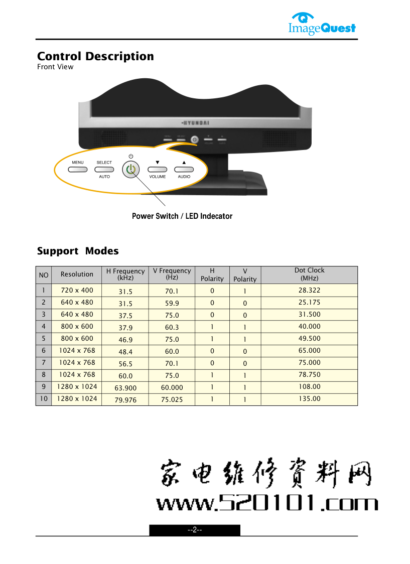
Control Description
Front View
Support Modes
H Frequency
(kHz)
31.5
31.5
37.5
37.9
46.9
48.4
56.5
60.0
63.900
79.976
V Frequency
(Hz)
70.1
59.9
75.0
60.3
75.0
60.0
70.1
75.0
60.000
75.025
H
Polarity
0
0
0
1
1
0
0
1
1
1
V
Polarity
1
0
0
1
1
0
0
1
1
1
Dot Clock
(MHz)
28.322
25.175
31.500
40.000
49.500
65.000
75.000
78.750
108.00
135.00
NO
1
2
3
4
5
6
7
8
9
10
Resolution
720 x 400
640 x 480
640 x 480
800 x 600
800 x 600
1024 x 768
1024 x 768
1024 x 768
1280 x 1024
1280 x 1024
Power Switch / LED Indecator
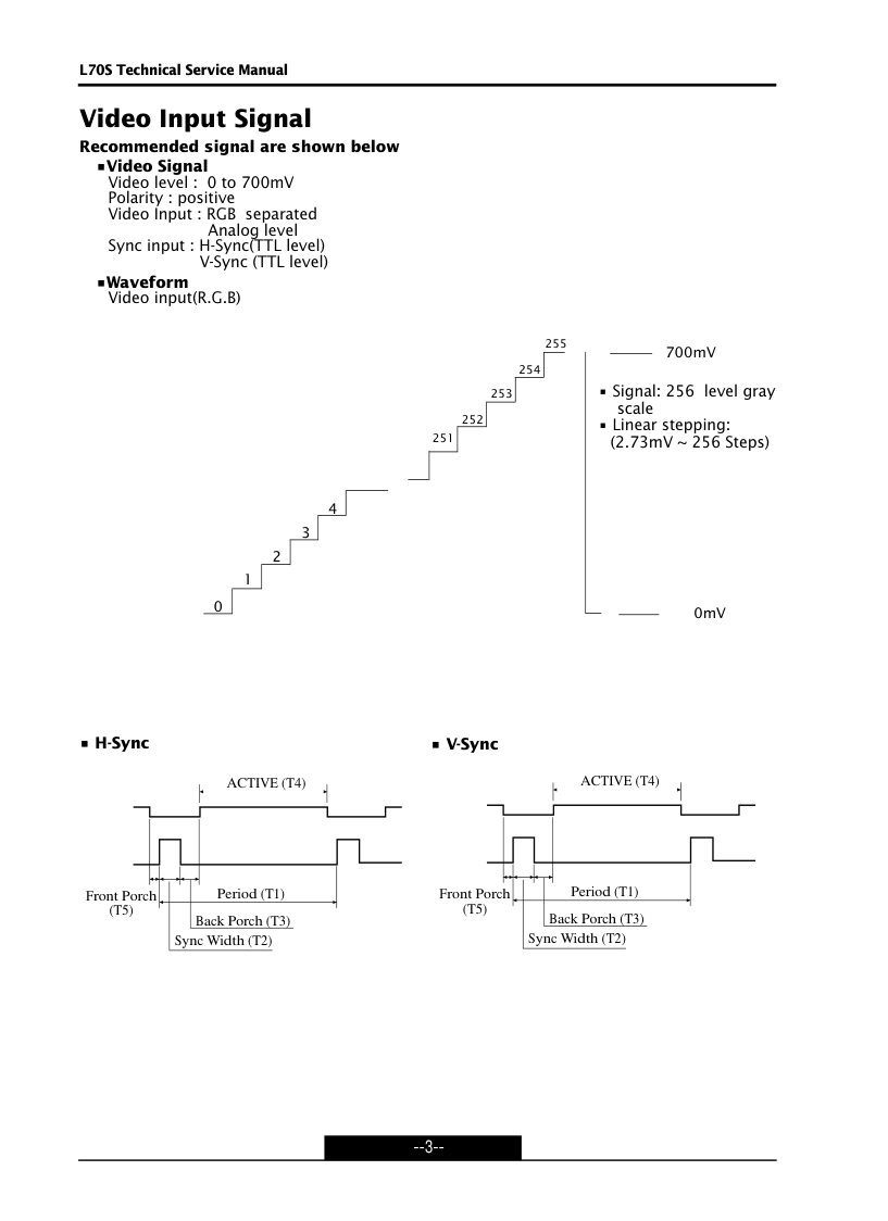
Video Input Signal
Recommended signal are shown below
•Video Signal
Video level : 0 to 700mV
Polarity : positive
Video Input : RGB separated
Analog level
Sync input : H-Sync(TTL level)
V-Sync (TTL level)
•Waveform
Video input(R.G.B)
--3--
L70S Technical Service Manual
ACTIVE (T4)
�
�
Front Porch�
(T5)
Period (T1)
Sync Width (T2)
Back Porch (T3)
ACTIVE (T4)
�
�
Front Porch�
(T5)
Period (T1)
Sync Width (T2)
Back Porch (T3)
• H-Sync
• V-Sync
0
1
2
3
4
251
252
253
254
255
700mV
0mV
• Signal: 256 level gray
scale
• Linear stepping:
(2.73mV ~ 256 Steps)
--4--
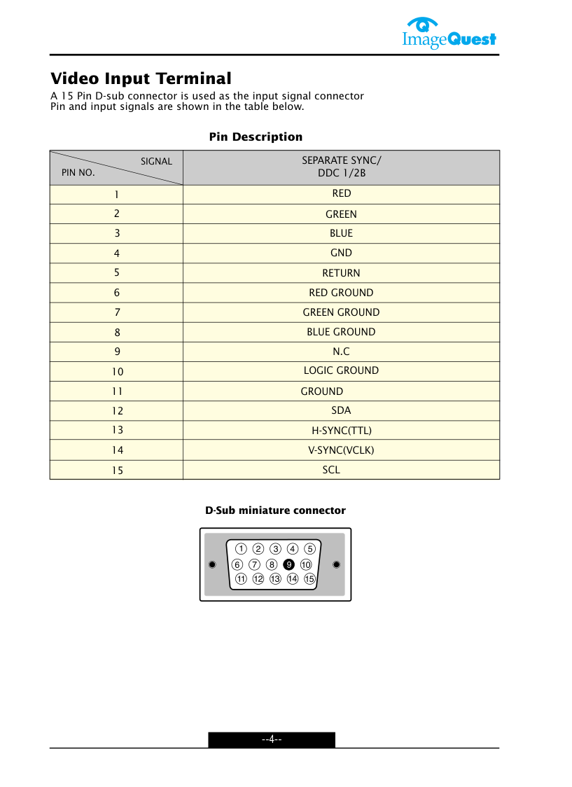
Video Input Terminal
A 15 Pin D-sub connector is used as the input signal connector
Pin and input signals are shown in the table below.
Pin Description
D-Sub miniature connector
SIGNAL
PIN NO.
3
2
1
5
4
6
7
8
9
10
11
12
13
14
SEPARATE SYNC/
DDC 1/2B
RED
GREEN
BLUE
GND
RETURN
RED GROUND
GREEN GROUND
BLUE GROUND
N.C
LOGIC GROUND
GROUND
SDA
H-SYNC(TTL)
V-SYNC(VCLK)
15
SCL
Connecting with External Equipment
Cautions
Be sure to turn off the power of your computer before connecting the monitor.
--5--
L70S Technical Service Manual
LINE OUT
--6--
Theory of Operation
1. AC/DC INVERTER
Input voltage : DC 12V
Input current : 2.0A(Max)
Output current : 6.5mArms(TYP)
Frequency(switching) : 47KHz(Max)
Output power : 18W(TYP)
On/off control voltage : 5.0V
2. AC/DC ADATOR
This display device shall maintain the specified per formances in the range de scribed
below
Frequency : 50/60Hz
Voltage : 90 - 264Vac RMS
The following consumption requirments shall be met:
Power Consumption : 35W(typ)
Current consumption : < 1.0 Aac RMS
Output Specification:
output1 : 12V/2A
output2 : 5V/1.5A
3. Audio System
This monitor has a audio system including two micro loudspeakers.
Each of two micro loudspeakers has a 2W(Max) output power.
This system also supports a headphone(earphone) output.
- Auto Signal Input : < 600mVp-p(Max.)
- Auto Amplifiers
2W+2W Amplifier with DC Volume Control (for two micro loudspeakers)
RL=8
@THD=10% Vcc=14V (min. 10V, max. 18V)
Dual-Audio Power Amplifier (for a headphone output)
RL=32
@THD=10% Vcc=4.5V (min. 1.8V, max. 15V)
- Speaker
Micro Loudspeaker Spec.
Normal impedance 8
15% at 1.0V 1.5KHz
Resonance Freq. 550Hz +/- 110Hz at 1.0V
Freq. Range fo ~ 20KHz
Power Rating Normal 1.0W/Peak 2.0W
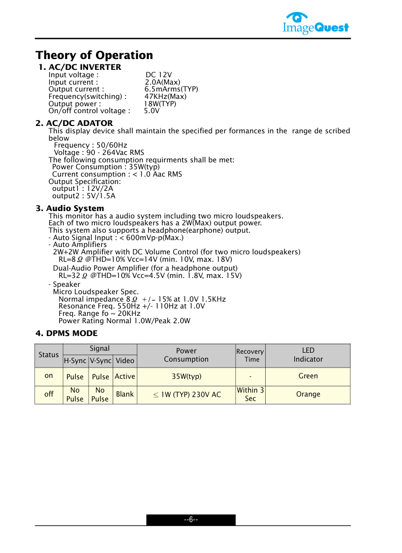
4. DPMS MODE
Status
on
Pulse
Pulse Active
Blank
No
Pulse
No
Pulse
off
Signal
Power
Consumption
-
Within 3
Sec
Recovery
Time
Orange
LED
Indicator
Green
35W(typ)
1W (TYP) 230V AC
H-Sync V-Sync Video
--7--
L70S Technical Service Manual
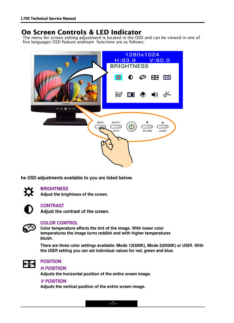
On Screen Controls & LED Indicator
The menu for screen setting adjustment is located in the OSD and can be viewed in one of
five languages OSD feature andmain funcrions are as follows:
he OSD adjustments available to you are listed below.
BRIGHTNESS
Adjust the brightness of the screen.
CONTRAST
Adjust the contrast of the screen.
COLOR CONTROL
Color temperature affects the tint of the image. With lower color
temperatures the image turns reddish and with higher temperatures
bluish.
There are three color settings available: Mode 1(9300K), Mode 2(6500K) or USER. With
the USER setting you can set individual values for red, green and blue.
POSITION
H POSITION
Adjusts the horizontal position of the entire screen image.
V POSITION
Adjusts the vertical position of the entire screen image.
1280x1024
H:63.9 V:60.0
BRIGHTNESS
BRIGHTNESS
--8--
CLOCK PHASE
PHASE
Adjust the noise of the screen image.
CLOCK
Adjust the horizontal size of the entire screen image.
MISCELLANEOUS
RECALL
Recall the saved color data.
OSD TIMER
You can set the displayed time of OSD Menu window on the screen by using this
adjustment.
OSD POSITION
Adjust the OSD menu's horizontal or vertical position on the screen.
AUTO COLOR
Optimum color setting is auto programmed for user’s convenience.
LANGUAGE
You can select the language in which adjustment menus are displayed.
The following languages are available : English, French, German, Italian,
Spanish, Swedish, Finnish, Danish, Portuguese, Dutch and Japanese or chinese.
AUDIO
VOLUME
Adjust the audio volume level.
AUDIO
This menu is used to choose audio on or off.
AUTO ADJUST
You can adjust the shape of screen automatically at the full screen pattern.
--9--
L70S Technical Service Manual
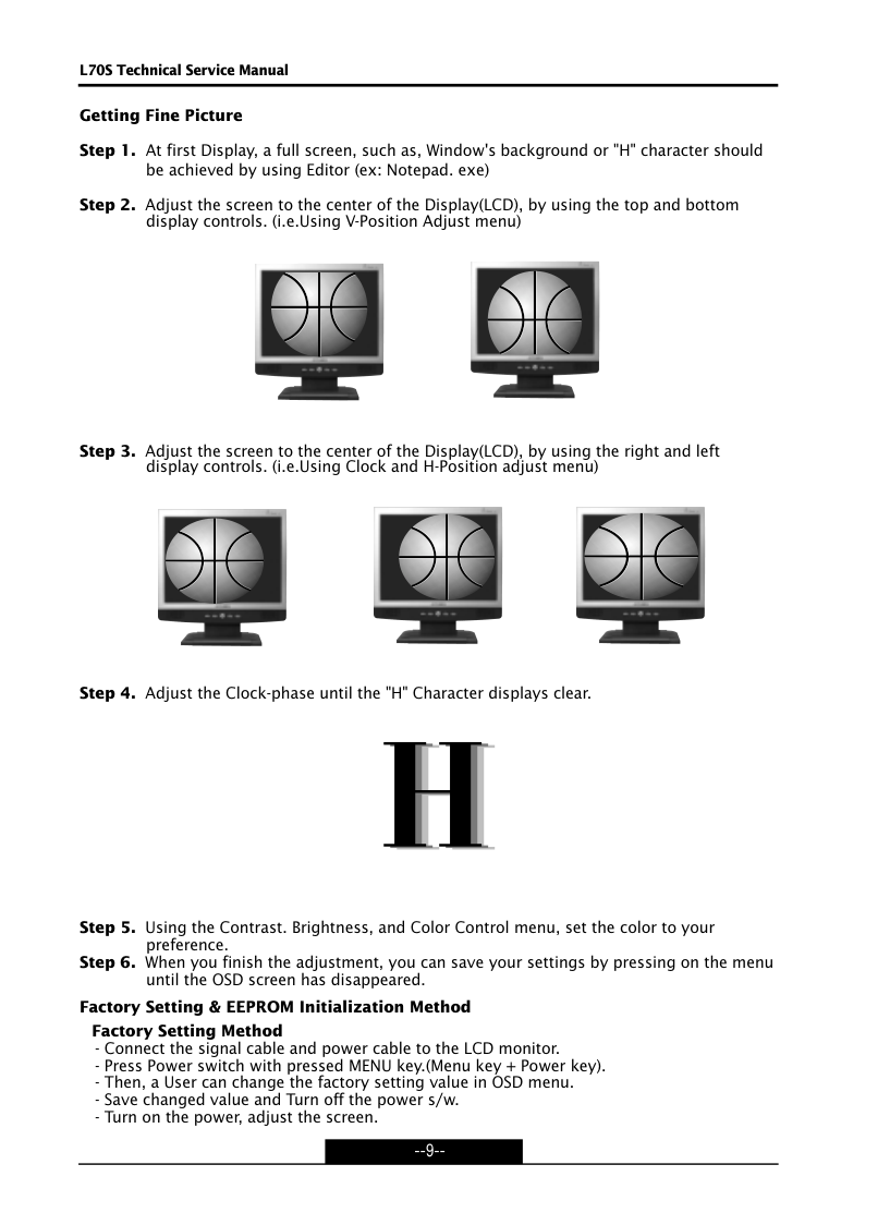
Getting Fine Picture
Step 1. At first Display, a full screen, such as, Window's background or "H" character should
be achieved by using Editor (ex: Notepad. exe)
Step 2. Adjust the screen to the center of the Display(LCD), by using the top and bottom
display controls. (i.e.Using V-Position Adjust menu)
Step 3. Adjust the screen to the center of the Display(LCD), by using the right and left
display controls. (i.e.Using Clock and H-Position adjust menu)
Step 4. Adjust the Clock-phase until the "H" Character displays clear.
Step 5. Using the Contrast. Brightness, and Color Control menu, set the color to your
preference.
Step 6. When you finish the adjustment, you can save your settings by pressing on the menu
until the OSD screen has disappeared.
Factory Setting & EEPROM Initialization Method
Factory Setting Method
- Connect the signal cable and power cable to the LCD monitor.
- Press Power switch with pressed MENU key.(Menu key + Power key).
- Then, a User can change the factory setting value in OSD menu.
- Save changed value and Turn off the power s/w.
- Turn on the power, adjust the screen.
--10--
Specification
LCD Module
SIZE
17” Viewable diagonal
Dot Pitch
0.264mm
Brightness
Response Time
260 cd/m2 (TYP)
16m- sec (Typ)
Input
Signal
R.G.B Analog
Connector
15 pin D-SUB Connector
SYNC
H-Freq
31.0kHz ~ 80.0kHz
V-Freq
56.0Hz ~ 75Hz
Display
Area
Color
337.92(H)X270.336(V)mm
262K Colors
Resolution
Video Bandwidth
User Control
&
OSD Control
Contrast,Brightness, Position, Auto Color,
Clock Phase, Color Control, Language,
Auto Adjust, Miscellaneous, Audio Control
Power Management
VESA DPMS Standard
Plug & Play
VESA DDC 1/2B
Safety &
Regulation
EMC
Ergonomi
Safety
FCC CLASS B , CE , VCCI
TCO’99
cULus, CE, TUV-GS, SEMKO
Temperature
30 to 80%(Non-condensing)
5 to 90%(Non-condensing)
packed
Humidity
Operating
Operating
Storage
Storage
5 to 35 °C
- 5 to 45 °C
Weight
unpacked
Dimension(WXHXD mm)
* Specification is subject to change without notice for performance improvement.
5.0Kg
372.5 X 398 X 185 mm
3.8Kg
1280 X 1024 @ 75Hz
135MHz
--11--
L70S Technical Service Manual
Critical Parts Specification
1. LCD Module
M170EN05(LTM170EU-L01, HT17E12-100 is a a-si TFT active matrix color liquid crystal
comprising amorphous silicon TFT attached to each signal electrode, a driving circuit and a
backlight.
M170EN05(LTM170EX-L01, HT17E12-100 has a built-in backlight display area contains
1280X1024 pixels and can display full color (262K colors)
Display area
337.92(H)X270.336(V)mm
Drive system
a-si TFT
Display color
262K Colors
Number of Pixel
1280X1024
Pixel arrangement
RGB vertical strip
Pixel pitch
0.264(H)X0.264(V)mm
Contrast Ratio*
450:1
Viewing angle*
Horizontal:
70 degree, 70 degree
Vertical:
70 degree, 70 degree
Response time*
16ms(Typ)
Luminance*
260cd/m2(Typ)
Signal system
Digital RGB signals, Sync signals(H, V-Sync),
Dot clock(DCLK) , DE(Data Enable)
Supply voltage
5V
Backlight
Edge light type: Four colt cathode fluorescent lamps
power consumption
19.6W(TYP) CCFL
*: only M170EN05
Vendor
Au Optronics
SamSung
Hydis
Type
M170EN05
LTM170EU-L01
HT17E12-100
--12--
Connector Name / Designation
Manufacturer
Type Parts Number
Mating Housing Part Number
Interface Connector / Interface card
JAE or compatible
FI-X30S-HF
FI-X30S-H
2) CONNECTIONS
Physical interface is described as for the connector on module.
These connectors are capable of accommodating the following signals and will be following
components
3) Signal Pin
Connector Name / Designation
Manufacturer
Type Parts Number
Mating Type Part Number
Lamp Connector / Backlight lamp
JST
BHR-04VS-1
SM04(4.0)B-BHS-1-TB
Pin#
1
3
5
7
9
11
13
15
17
19
21
23
25
27
29
Pin#
2
4
6
8
10
12
14
16
18
20
22
24
26
28
30
Signal Name
Rxo0-
Rxo1-
Rxo2-
GND
RxoC+
Rxo3+
RxEo+
RxE1-
GND
RxE2+
RxEC+
RxE3+
NC
NC
Power
Signal Name
Rxo0+
Rxo1+
Rxo2+
RxoC-
Rxo3-
RxE0-
GND
RxE1+
RxE2-
RxEC-
RxE3-
GND
NC
Power
Power
4) Signal Description
The module using a pair of LVDS receiver SN75LVDS82 (Texas Instruments) or compatible.
LVDS is a differential signal technology for LCD interface and high speed data transfer
device. Transmitter shall be SN75LVDS83(negative edge sampling)or compatible. The first
LVDS port(RxOxxx)transmots odd pixels while the second LVDS port(RxExxxx)transmits
even pixels.
Note : Input signals of odd and even clock shall be the same timing.
--13--
L70S Technical Service Manual
PIN #
1
2
3
4
5
6
7
8
9
10
11
12
13
14
15
16
17
18
19
20
21
22
23
24
25
26
27
28
29
30
SIGNAL NAME
RxO0-
RxO0+
RxO1-
RxO1+
RxO2-
RxO2+
GND
RxOC-
RxOC+
RxO3-
RxO3+
RxE0-
RxE0+
GND
RxE1-
RxE1+
GND
RxE2-
RxE2+
RxEC-
RxEC+
RxE3-
RxE3+
GND
NC
NC
NC
POWER
POWER
POWER
DESCRIPTION
Negative LVDS differential data input (odd data)
Positive LVDS differential data input (odd data)
Negative LVDS differential data input (odd data)
Positive LVDS differential data input (odd data)
Negative LVDS differential data input (odd data, H-Sync, V-Sync,DSPTMG)
Positive LVDS differential data input (odd data, H-Sync, V-Sync,DSPTMG)
Power Ground
Negative LVDS differential clock input (odd clock)
Positive LVDS differential clock input (odd clock)
Negative LVDS differential data input (odd data)
Positive LVDS differential data input (odd data)
Negative LVDS differential data input (Even clock)
Positive LVDS differential data input (Even data)
Power Ground
Positive LVDS differential data input (Even data)
Negative LVDS differential data input (Even data)
Power Ground
Negative LVDS differential data input (Even data)
Positive LVDS differential data input (Even data)
Negative LVDS differential clock input (Even clock)
Positive LVDS differential clock input (Even clock)
Negative LVDS differential data input (Even data)
Positive LVDS differential data input (Even data)
Power Ground
-
-
-
Power
Power
Power
LVDS DATA Name
DSP
V-S
H-S
DESCRIPTION
Display Timing : When the signal is high, the pixel data shall be valid to be displayed
Vertical Sync : Both Positive and Negative polarity are acceptable
Horizontal Sync : Both Positive and Negative polarity are acceptable
--14--
GENERAL DESCRI PTION
The MST9111 is a high performance, and fully integrated graphics processing IC solution for LCD
monitors with resolutions up to SXGA. It is configured with an integrated triple-ADC/PLL, a high qualit
scaling engine, an on-screen display controller, a built-in output clock generator, and LVDS displa
interface. To further reduce system costs, the MST9111 also integrates intelligent power managemen
control capability for green-mode requirements and spread-spectrum support for EMI management.
FEATURES
¡
¡
¡
¡
¡
¡
¡
¡
¡
¡
¡
¡
¡
¡
¡
¡
¡
¡
¡
¡
¡
¡
¡
¡
¡
¡
¡
¡
¡
¡
¡
¡
¡
¡
¡
¡
High-quality zoom and shrink scaling engine
(Compatible with VGA thru SXGA)
Integrated 8-bit triple-ADC/PLL
On-screen display controller (OSD)
Support single-RGB inputs
Built-in LVDS transmitter
Support composite sync and SOG separator
Programmable 10-bit gamma correction
Integrated Brightness & Contrast control
adjustment
Support PWM backlit intensity control
Support sRGB function
Green PC and low EMI features
Low standby power mode (< 5mA)
High-Performance Scaling Engine
Programmable shrink/zoom capabilities
High-quality scaling for all VESA and IBM mode
to fit screen
Variable sharpness control
Analog RGB Compliant Input Port
Supports up to SXGA at 85Hz
Supports Composite Sync and SOG
(Sync-on-Green) separator
Auto-Detection/Tune
Auto input signal format (SOG, Composite,
Separated HSYNC, VSYNC, and DE), and input
mode (all VESA & IBM modes w/ resolution and
polarity) detection
Auto-tuning function
including
phasing,
positioning, offset, gain, and jitter detection
Smart screen-fitting
On-Screen OSD Controller
Built-in OSD generator with 226 character font
programmable RAM
Internal OSD rotation degree of 90 and 270
Gradient color function
Pattern generator for production test
Support OSD MUX and alpha blending capability
LVDS Display Interface
Dual pixel with max. output LVDS clock rate of 85
MHz
Support 2 data output formats: Thine & TI data
mappings
Compatible with TIA/EIA
With 6/8 bits options
Reduced swing for LVDS for low EMI
External Connection/Component
Built-in DDC circuit
MST9111
L70S Technical Service Manual
PIN DIAGRAM
--16--
Pin Name
A0, A1
N.C.
A2
Device Address inputs
Vss
Ground
SDA
Data I/O
SCL
Clock input
WP
Write Protect
Vcc
+ 5 V or + 3 V
3.0 ABSOLUTE MAXIMUM RATINGS
Storage Temperature................................-65°C to + 125°C
Voltage with Respect to Ground.................-0.3 to + 6.5 V
NOTE: These are STRESS rating only. Appropriate conditions for operating these devices given elsewhere
may permanently damage the part. Prolonged exposure to maximum ratings may affect device reliability.
4.0 OPERATING CONDITIONS
Temperature under bias: MTV24C08/24LC08.......0°C to + 70°C
MTV24C08/24LC08-I.....-40°C to + 85°C
VCC
WP
SCL
SDA
A0
A1
A2
VSS
1
2
3
4
5
6
7
8
24C08
or
24LC08
TSSOP
VCC
WP
SCL
SDA
A0
A1
A2
VSS
VCC
WP
SCL
SDA
A0
A1
A2
VSS
1
2
3
4
8
7
6
5
1
2
3
4
5
6
7
8
Dual-In-Line
package
SO package
(M8)
24C08
or
24LC08
24C08
or
24LC08
24LC08
--17--
L70S Technical Service Manual
5.0 ELECTRICAL CHARACTERISTICS
DC ELECTRICAL CHARACTERISTICS
(Vcc =5V +/- 10% ,MTV24C08/24LC08°
FVcc =3V +/- 10% ,24LC08)
MTV24C08/
24LC08
24LC08
Units
Symbol
Parameter
Conditions
Min
Max
Min
Max
ICC1
Operating Current
(Program)
SCL = 100KHZ
CMOS Input Levels
—
10
—
8
mA
ICC2
Operating Current
(Read)
SCL = 100KHZ
CMOS Input Levels
—
2
—
2
mA
ISB
Standby Current
SCL = SDA = 0 V
—
10
—
10
µA
IIL
Input Leakage
VIN = 0 V to VCC
-1
+1
-1
+1
µA
IOL
Output Leakage
VOUT = 0 V to Vcc
-1
+1
-1
+1
µA
VIL
Input Low Voltage
-0.1
0.8
-0.1
0.15 VCC
V
VIH
Input High Voltage
2
VCC +0.2
0.8VCC
VCC+0.2
V
VOL1
Output Low Voltage
IOL = 2.1mA TTL
—
0.4
—
0.4
V
VOH1
Output High Voltage
IOH = -400uA TTL
2.4
—
2.4
—
V
VOL2
Output Low Voltage
IOL = 10uA CMOS
—
0.2
—
0.2
V
VOH2
Output High Voltage
IOH = -10uA CMOS
VCC-0.2
—
VCC-0.2
—
V
VLK
VCC Lockout Voltage
Programming Command
Can Be Executed
Default
—
Default
—
V
6.0 SWITCHING CHACTERISTICS (Under Operating Conditions )
AC ELECTRICAL CHARACTERISTICS
(Vcc =5V +/- 10% , MTV24C08°
FVcc =3V +/- 10% ,24LC08)
(Vcc =5V +/- 10% , MTV24C08 Fast Mode)
MTV24C08/
24LC08
MTV24C08
(Fast Mode)
Parameter
Symbol
Min
Max
Min
Max
Units
Clock frequency
Fscl
0
100
—
400
kHz
Clock high time
Thigh
4000
—
600
—
ns
Clock low time
Tlow
4700
—
1200
—
ns
SDA and SCL rise time
Tr
—
1000
—
300
ns
SDA and SCL fall time
Tf
—
300
—
300
ns
START condition hold time
Thd:Sta
4000
—
600
—
ns
START condition setup time
Tsu:Sta
4700
—
600
—
ns
Data input hold time
Thd:Dat
0
—
0
—
ns
Data input setup time
Tsu:Dat
250
—
100
—
ns
STOP condition setup time
Tsu:Sto
4000
—
600
—
ns
Output valid from clock
Taa
300
3500
100
900
ns
Bus free time
Tbuf
4700
—
1200
—
ns
Data out hold time
Tdh
300
—
50
—
ns
Input filter spike suppression
(SDA and SCL pins)
Tsp
—
100
—
50
ns
Write cycle time
Twr
—
10
—
10
ms
--18--
CAPACITANCE TA= 25∞C , f=250KHZ
Symbol
Parameter
Max
Units
CO
UT
Output capacitance
5
pF
CIN
Input capacitance
5
pF
A. C. Conditions of Test
Input Pulse Levels
Vcc x 0.1 to Vcc x 0.9
Input Rise and Fall times
10 ns
Input and Output Timming level
Vcc x 0.5
Output Load
1 TTL Gate and CL = 100pf
--19--
L70S Technical Service Manual
Features
•� Low dropout voltage
•� Load regulation: 0.05% typical
•� Trimmed current limit
•� On-chip thermal limiting
•� Standard SOT-223, TO-263, and TO-252 packages
•� Three-terminal adjustable or fixed 2.5V, 2.85V, 3.3V, 5V
Applications
•� Active SCSI terminators
•� High efficiency linear regulators
•� Post regulators for switching supplies
•� Battery chargers
•� 5V to 3.3V linear regulators
•� Motherboard clock supplies
Description
The RC1117 and RC1117-2.5, -2.85, -3.3 and -5 are low
dropout three-terminal regulators with 1A output current
capability. These devices have been optimized for low voltage
where transient response and minimum input voltage are
critical. The 2.85V version is designed specifically to be
used in Active Terminators for SCSI bus.
Current limit is trimmed to ensure specified output current
and controlled short-circuit current. On-chip thermal limiting
provides protection against any combination of overload and
ambient temperatures that would create excessive junction
temperatures.
Unlike PNP type regulators where up to 10% of the output
current is wasted as quiescent current, the quiescent current
of the RC1117 flows into the load, increasing efficiency.
The RC1117 series regulators are available in the industry-
standard SOT-223, TO-263 (D2PAK), and TO-252 (DPAK)
power packages.
Typical Applications
VIN = 3.3V
VIN
VOUT
ADJ
1.5V at 1A
RC1117
10 F
2
2 F
R1
124
R2
24.9
VIN = 5V
VIN
VOUT
GND
2.85V at 1A
RC1117-2.85
10 F
+
+
+
+
22 F
VOUT = VREF(1 + R2/R1) + IAdj • R2
RC1117
1A Adjustable/Fixed Low Dropout Linear Regulator
RC1117X2.5
--20--
Pin Assignments
*With package soldered to 0.5 square inch copper area over backside ground plane or internal power plane.,
JA can vary from
30°C/W to more than 50°C/W. Other mounting techniques may provide better thermal resistance than 30°C/W.
Absolute Maximum Ratings
Parameter
Min.
Max.
Unit
VIN
7.5
V
Operating Junction Temperature Range
0
125
C
Storage Temperature Range
-65
150
C
Lead Temperature (Soldering, 10 sec.)
300
C
Front View
4-Lead Plastic SOT-223
JC = 15 C/W*
3-Lead Plastic TO-252
JC = 3 C/W*
Tab is
VOUT
Tab is
VOUT
1
ADJ/
GND
IN
2
3
3-Lead Plastic TO-263
JC = 3 C/W*
Tab is
VOUT
1
ADJ/
GND
IN
OUT
2
3
3
2
1
IN
OUT
ADJ/GND
--21--
L70S Technical Service Manual
Electrical Characteristics
Operating Conditions: VIN 7V, TJ = 25°�C unless otherwise specifi�ed.
The denotes specifi�cations which apply over the specifi�ed operating temperature range.
Notes:
1. See thermal regulation specifications for changes in output voltage due to heating effects. Load and line regulation are
measured at a constant junction temperature by low duty cycle pulse testing.
2. Line and load regulation are guaranteed up to the maximum power dissipation (18W). Power dissipation is determined by
input/output differential and the output current. Guaranteed maximum output power will not be available over the full input/
output voltage range.
3. RC1117 only.
Parameter
Conditions
Min.
Typ.
Max.
Units
Reference Voltage, VREF
3
1.5V (VIN - VOUT) 5.75V,
10mA IOUT 1A
1.225
(-2%)
1.250
1.275
(+2%)
V
Output Voltage
10mA IOUT 1A
RC1117-2.5, 4V VIN 7V
RC1117-2.85, 4.35V VIN 7V
RC1117-3.3, 4.8V VIN 7V
RC1117-5, 6.5V VIN 7V
2.450
2.793
3.234
4.900
2.5
2.85
3.3
5.0
2.550
2.907
3.366
5.100
V
V
V
V
Line Regulation1,2
(VOUT + 1.5V) VIN 7V, IOUT = 10mA
0.005
0.2
%
Load Regulation1,2
(VIN –� VOUT) = 2V, 10mA IOUT 1A
0.05
0.5
%
Dropout Voltage
VREF = 1%, IOUT = 1A
1.100
1.200
V
Current Limit
(VIN –� VOUT) = 2V
1.1
1.5
A
Adjust Pin Current, IAdj
3
35
120
A
Adjust Pin Current Change3
1.5V (VIN –� VOUT) 5.75,
10mA IOUT 1A
0.2
5
A
Minimum Load Current
1.5V (VIN –� VOUT) 5.75
10
mA
Quiescent Current
VIN = VOUT + 1.25V
4
13
mA
Ripple Rejection
f = 120Hz, COUT = 22 F Tantalum,
(VIN –� VOUT) = 3V, IOUT = 1A
60
72
dB
Thermal Regulation
TA = 25 C, 30ms pulse
0.004
0.02
%/W
Temperature Stability
0.5
%
Long-Term Stability
TA = 125 C, 1000hrs.
0.03
1.0
%
RMS Output Noise
(% of VOUT)
TA = 25 C, 10Hz f 10kHz
0.003
%
Thermal Resistance, Junction
to Case
SOT-223
15
C/W
TO-252, TO-263
3
C/W
Thermal Shutdown
Junction Temperature
155
C
Thermal Shutdown
Hysteresis
10
C
--22--
RC1117-3.3
Features
•� Low dropout voltage
•� Load regulation: 0.05% typical
•� Trimmed current limit
•� On-chip thermal limiting
•� Standard SOT-223, TO-263, and TO-252 packages
•� Three-terminal adjustable or fixed 2.5V, 2.85V, 3.3V, 5V
Applications
•� Active SCSI terminators
•� High efficiency linear regulators
•� Post regulators for switching supplies
•� Battery chargers
•� 5V to 3.3V linear regulators
•� Motherboard clock supplies
Description
The RC1117 and RC1117-2.5, -2.85, -3.3 and -5 are low
dropout three-terminal regulators with 1A output current
capability. These devices have been optimized for low voltage
where transient response and minimum input voltage are
critical. The 2.85V version is designed specifically to be
used in Active Terminators for SCSI bus.
Current limit is trimmed to ensure specified output current
and controlled short-circuit current. On-chip thermal limiting
provides protection against any combination of overload and
ambient temperatures that would create excessive junction
temperatures.
Unlike PNP type regulators where up to 10% of the output
current is wasted as quiescent current, the quiescent current
of the RC1117 flows into the load, increasing efficiency.
The RC1117 series regulators are available in the industry-
standard SOT-223, TO-263 (D2PAK), and TO-252 (DPAK)
power packages.
Typical Applications
VIN = 3.3V
VIN
VOUT
ADJ
1.5V at 1A
RC1117
10 F
2
2 F
R1
124
R2
24.9
VIN = 5V
VIN
VOUT
GND
2.85V at 1A
RC1117-2.85
10 F
+
+
+
+
22 F
VOUT = VREF(1 + R2/R1) + IAdj • R2
1A Adjustable/Fixed Low Dropout Linear Regulator
--23--
L70S Technical Service Manual
Pin Assignments
*With package soldered to 0.5 square inch copper area over backside ground plane or internal power plane.,
JA can vary from
30°C/W to more than 50°C/W. Other mounting techniques may provide better thermal resistance than 30°C/W.
Absolute Maximum Ratings
Parameter
Min.
Max.
Unit
VIN
7.5
V
Operating Junction Temperature Range
0
125
C
Storage Temperature Range
-65
150
C
Lead Temperature (Soldering, 10 sec.)
300
C
Front View
4-Lead Plastic SOT-223
JC = 15 C/W*
3-Lead Plastic TO-252
JC = 3 C/W*
Tab is
VOUT
Tab is
VOUT
1
ADJ/
GND
IN
2
3
3-Lead Plastic TO-263
JC = 3 C/W*
Tab is
VOUT
1
ADJ/
GND
IN
OUT
2
3
3
2
1
IN
OUT
ADJ/GND
--24--
Electrical Characteristics
Operating Conditions: VIN 7V, TJ = 25°�C unless otherwise specifi�ed.
The denotes specifi�cations which apply over the specifi�ed operating temperature range.
Notes:
1. See thermal regulation specifications for changes in output voltage due to heating effects. Load and line regulation are
measured at a constant junction temperature by low duty cycle pulse testing.
2. Line and load regulation are guaranteed up to the maximum power dissipation (18W). Power dissipation is determined by
input/output differential and the output current. Guaranteed maximum output power will not be available over the full input/
output voltage range.
3. RC1117 only.
Parameter
Conditions
Min.
Typ.
Max.
Units
Reference Voltage, VREF
3
1.5V (VIN - VOUT) 5.75V,
10mA IOUT 1A
1.225
(-2%)
1.250
1.275
(+2%)
V
Output Voltage
10mA IOUT 1A
RC1117-2.5, 4V VIN 7V
RC1117-2.85, 4.35V VIN 7V
RC1117-3.3, 4.8V VIN 7V
RC1117-5, 6.5V VIN 7V
2.450
2.793
3.234
4.900
2.5
2.85
3.3
5.0
2.550
2.907
3.366
5.100
V
V
V
V
Line Regulation1,2
(VOUT + 1.5V) VIN 7V, IOUT = 10mA
0.005
0.2
%
Load Regulation1,2
(VIN –� VOUT) = 2V, 10mA IOUT 1A
0.05
0.5
%
Dropout Voltage
VREF = 1%, IOUT = 1A
1.100
1.200
V
Current Limit
(VIN –� VOUT) = 2V
1.1
1.5
A
Adjust Pin Current, IAdj
3
35
120
A
Adjust Pin Current Change3
1.5V (VIN –� VOUT) 5.75,
10mA IOUT 1A
0.2
5
A
Minimum Load Current
1.5V (VIN –� VOUT) 5.75
10
mA
Quiescent Current
VIN = VOUT + 1.25V
4
13
mA
Ripple Rejection
f = 120Hz, COUT = 22 F Tantalum,
(VIN –� VOUT) = 3V, IOUT = 1A
60
72
dB
Thermal Regulation
TA = 25 C, 30ms pulse
0.004
0.02
%/W
Temperature Stability
0.5
%
Long-Term Stability
TA = 125 C, 1000hrs.
0.03
1.0
%
RMS Output Noise
(% of VOUT)
TA = 25 C, 10Hz f 10kHz
0.003
%
Thermal Resistance, Junction
to Case
SOT-223
15
C/W
TO-252, TO-263
3
C/W
Thermal Shutdown
Junction Temperature
155
C
Thermal Shutdown
Hysteresis
10
C
--25--
L70S Technical Service Manual
SI4435
Parameter
Max.
Units
VDS
Drain- Source Voltage
-30
V
ID @ TA = 25∞C
Continuous Drain Current, VGS @ -10V
-8.0
ID @ TA= 70∞C
Continuous Drain Current, VGS @ -10V
-6.4
A
IDM
Pulsed Drain Current Å
-50
PD @TA = 25∞C
Power Dissipation
2.5
PD @TA = 70∞C
Power Dissipation
1.6
Linear Derating Factor
0.02
W/ C
VGS
Gate-to-Source Voltage
± 20
V
TJ, TSTG
Junction and Storage Temperature Range
-55 to + 150
C
Parameter
Max.
Units
RθJA
Maximum Junction-to-AmbientÉ
50
C/W
Thermal Resistance
Absolute Maximum Ratings
W
Si4435DY
HEXFET� Power MOSFET
These P-channel HEXFET� Power MOSFETs from
International Rectifier utilize advanced processing
techniques to achieve the extremely low on-resistance per
silicon area. This benefit provides the designer with an
extremely efficient device for use in battery and load
management applications..
The SO-8 has been modified through a customized
leadframe for enhanced thermal characteristics and
multiple-die capability making it ideal in a variety of power
applications. With these improvements, multiple devices
can be used in an application with dramatically reduced
board space. The package is designed for vapor phase,
infrared, or wave soldering techniques.
VDSS = -30V
RDS(on) = 0.020Ω
Description
Ultra Low On-Resistance
P-Channel MOSFET
Surface Mount
Available in Tape & Reel
PD- 93768A
Top View
8
1
2
3
4
5
6
7
D
D
D
G
S
A
D
S
S
SO-8
-
-
-
-
o
o
o
--26--
Si4435DY
Parameter
Min. Typ. Max.
Units
Conditions
IS
Continuous Source Current
MOSFET symbol
(Body Diode)
showing the
ISM
Pulsed Source Current
integral reverse
(Body Diode) Å
p-n junction diode.
VSD
Diode Forward Voltage
ñññ�
ñññ�
-1.2
V
TJ = 25∞C, IS = -2.5A, VGS = 0V Ç
trr
Reverse Recovery Time
ñ�ñ�ñ�
34
51
ns
TJ = 25∞C, IF = -2.5A
Qrr
Reverse Recovery Charge
ñ�ñ�ñ�
33
50
nC
di/dt = -100A/µs Ç
Source-Drain Ratings and Characteristics
A
-50
ñññ�
ñññ�
ñññ�
-2.5
ñññ�
S
D
G
Å Repetitive rating; pulse width limited by
max. junction temperature.
Notes:
Ç Pulse width ≤ 300µs; duty cycle ≤ 2%.
É Surface mounted on FR-4 board, t ≤ 5sec.
Parameter
Min. Typ. Max.
Units
Conditions
V(BR)DSS
Drain-to-Source Breakdown Voltage
-30
ñ�ñ�ñ�
ñ�ñ�ñ�
V
VGS = 0V, ID = -250µA
∆V(BR)DSS/∆TJ
Breakdown Voltage Temp. Coefficient
ñ�ñ�ñ� -0.019 ñ�ñ�ñ�
V/∞C Reference to 25∞C, ID = -1mA
ñññ� 0.015 0.020
VGS = -10V, ID = -8.0A Ç
ñññ� 0.026 0.035
VGS = -4.5V, ID = -5.0A Ç
VGS(th)
Gate Threshold Voltage
-1.0
ñññ�
ñññ�
V
VDS = VGS, ID = -250µA
gfs
Forward Transconductance
ñ�ñ�ñ�
11
ñ�ñ�ñ�
S
VDS = -15V, ID = -8.0A
ñññ�
ñññ�
-10
VDS = -24V, VGS = 0V
ñññ�
ñññ�
-10
VDS = -15V, VGS = 0V, TJ = 70∞C
Gate-to-Source Forward Leakage
ñññ�
ñññ� -100
VGS = -20V
Gate-to-Source Reverse Leakage
ñ�ñ�ñ�
ñ�ñ�ñ�
100
VGS = 20V
Qg
Total Gate Charge
ñ�ñ�ñ�
40
60
ID = -4.6A
Qgs
Gate-to-Source Charge
ñ�ñ�ñ�
7.1
ñ�ñ�ñ�
nC
VDS = -15V
Qgd
Gate-to-Drain ("Miller") Charge
ñ�ñ�ñ�
8.0
ñ�ñ�ñ�
VGS = -10V Ç
td(on)
Turn-On Delay Time
ñ�ñ�ñ�
16
24
VDD = -15V, VGS = -10V Ç
tr
Rise Time
ñññ�
76
110
ID = -1.0A
td(off)
Turn-Off Delay Time
ñ�ñ�ñ�
130
200
RG = 6.0Ω
tf
Fall Time
ñññ�
90
140
RD = 15Ω
Ciss
Input Capacitance
ñ�ñ�ñ� 2320
ñ�ñ�ñ�
VGS = 0V
Coss
Output Capacitance
ñ�ñ�ñ�
390
ñ�ñ�ñ�
pF
VDS = -15V
Crss
Reverse Transfer Capacitance
ñ�ñ�ñ�
270
ñ�ñ�ñ�
É = 1.0kHz
Electrical Characteristics @ TJ = 25∞C (unless otherwise specified)
IGSS
µA
Ω
RDS(on)
Static Drain-to-Source On-Resistance
IDSS
Drain-to-Source Leakage Current
nA
ns
--27--
L70S Technical Service Manual
TDA7496L
2W+2W OUTPUT POWER
RL = 8Ω @THD = 10% VCC = 14V
ST-BY AND MUTE FUNCTIONS
LOW TURN-ON TURN-OFF POP NOISE
LINEAR VOLUME CONTROL DC COUPLED
WITH POWER OP. AMP.
NO BOUCHEROT CELL
NO ST-BY RC INPUT NETWORK
SINGLE SUPPLY RANGING UP TO 15V
SHORT CIRCUIT PROTECTION
THERMAL OVERLOAD PROTECTION
INTERNALLY FIXED GAIN
SOFT CLIPPING
VARIABLE OUTPUT AFTER VOLUME CON-
TROL CIRCUIT
POWERDIP (14+3+3) PACKAGE
DESCRIPTION
The TDA7496L is a stereo 2W+2W class AB
power amplifier assembled in the @ Powerdip
14+3+3 package, specially designed for high
quality sound, TV and Monitor applications.
Features of the TDA7496L include linear volume
control, Stand-by and mute functions.
VOLUME
OP AMP
+
-
MUTE/STBY
PROTECTIONS
9
470nF
INR
30K
VOLUME
OP AMP
+
-
30K
1000µF
1000µF
1µF
10K
4
470nF
INL
7
14
11
12
17
6
5
300K
100nF
VOLUME
VAROUT_L
OUTR
STBY
MUTE
OUTL
1,2,3,13,
18,19,20
GND
470µF
SVR
10
D97AU596A
VS
VAROUT_R
15,16
+5V
S1 ST-BY
+5V
S2 MUTE
+5V
S_GND
60K
BLOCK DIAGRAM
Powerdip (14+3+3)
ORDERING NUMBER: TDA7496L
2W+2W AMPLIFIER WITH DC VOLUME CONTROL
--28--
GND
GND
GND
INL
VAROUT_L
VAROUT_R
VOLUME
N.C.
INR
1
3
2
4
5
6
7
8
9
MUTE
GND
OUTR
VS
VS
OUTL
GND
GND
GND
20
19
18
17
16
14
15
13
12
D97AU597A
SVR
10
STBY
11
PIN CONNECTION
THERMAL DATA
Symbol
Parameter
Value
Unit
Rth j-pins
Thermal Resistance Junction-pins max.
15
∞�C/W
Rth j-amb (*)
Thermal Resistance Junction-ambient max.
50
∞�C/W
(*) Mounted on PCB with no heatsink
ELECTRICAL CHARACTERISTICS (Refer to the test circuit VS = 14V; RL = 8Ω, Rg = 50Ω, Tamb = 25∞�C).
Symbol
Parameter
Test Condition
Min.
Typ.
Max.
Unit
VS
Supply Voltage Range
10
18
V
Iq
Total Quiescent Current
25
50
mA
DCVOS
Output DC Offset Referred to
SVR Potenial
No Input Signal
200
mV
VO
Quiescent Output Voltage
7
V
PO
Output Power
THD = 10%; RL = 8Ω;
1
.6
2
W
THD = 1%; RL = 8Ω;
1
.3
W
THD
Total Harmonic Distortion
GV = 30dB; PO = 1W; f = 1KHz;
0.4
%
Ipeak
Output Peak Current
(internally limited)
0.7
0.9
A
Vin
Input Signal
2.8
Vrms
GV
Closed Loop Gain
Vol Ctrl > 4.5V
28.5
30
31.5
dB
GvLine
Monitor Out Gain
Vol Ctrl > 4.5V; Zload > 30KΩ
-1.5
0
1.5
dB
AMin VOL
Attenuation at Minimum Volume
Vol Ctrl < 0.5V
80
dB
BW
0.6
MHz
ABSOLUTE MAXIMUM RATINGS
Symbol
Parameter
Value
Unit
VS
DC Supply Voltage
26
V
VIN
Maximum Input Voltage
8
Vpp
Ptot
Total Power Dissipation (Tcase = 60∞�C)
6
W
Tamb
Ambient Operating Temperature
0 to 70
∞�C
Tstg, Tj
Storage and Junction Temperature
-40 to 150
∞�C
V6
Volume CTRL DC voltage
7
V
0
4
8
12
Area(cm2)
30
40
50
60
Rthj-a
(∞C/W)
D97AU675
COPPER AREA 35µ
THICKNESS
PC BOARD
Rth with "on board" Square Heatsink vs. cop-
per area.
--29--
L70S Technical Service Manual
ELECTRICAL CHARACTERISTICS (continued)
Symbol
Parameter
Test Condition
Min.
Typ.
Max.
Unit
eN
Total Output Noise
f = 20Hz to 22KHz
Play, max volume
500
800
µV
f = 20Hz to 22KHz
Play, max attenuation
100
250
µV
f = 20Hz to 22KHz
Mute
60
150
µV
SR
Slew Rate
5
8
V/µs
Ri
Input Resistance
22.5
30
KΩ
RVar Out
Variable Output Resistance
30
100
Ω
Rload Var Out
Variable Output Load
2
KΩ
SVR
Supply Voltage Rejection
f = 1kHz; max volume
CSVR = 470µF; VRIP = 1Vrms
35
39
dB
f = 1kHz; max attenuation
CSVR = 470µF; VRIP =1Vrms
55
65
dB
TM
Thermal Muting
150
∞�C
Ts
Thermal Shut-down
160
∞�C
MUTE STAND-BY & INPUT SELECTION FUNCTIONS
VST ON
Stand-by ON Threshold
3.5
V
VST OFF
Stand-by OFF Threshold
1.5
V
VM ON
Mute ON Threshold
3.5
V
VM OFF
Mute OFF Threshold
1.5
V
IqST-BY
Quiescent Current @ Stand-by
0.6
1
mA
AMUTE
Mute Attenuation
50
65
dB
IstbyBIAS
Stand-by bias current
Stand by on VST-BY = 5V
VMUTE = 5V
80
µA
µA
Play or Mute
-20
-5
µA
ImuteBIAS
Mute bias current
Mute
1
5
µA
Play
0.2
2
µA
APPLICATION SUGGESTIONS
The recommended values of the external components are those shown on the application circuit of fig-
ure 1A. Different values can be used, the following table can help the designer.
COMPONENT
SUGGESTION
VALUE
PURPOSE
LARGER THAN
SUGGESTION
SMALLER THAN
SUGGESTION
R1
300K
Volume control
circuit
Larger volume regulation
time
Smaller volume regulation
time
R2
10K
Mute time constant
Larger mute on/off time
Smaller mute on/off time
P1
50K
Volume control
circuit
C1
1000µF
Supply voltage
bypass
Danger of oscillation
C2
470nF
Input DC decoupling
Lower low frequency cutoff
Higher low frequency cutoff
C3
470nF
Input DC decoupling
Lower low frequency cutoff
Higher low frequency cutoff
C4
470µF
Ripple rejection
Better SVR
Worse SVR
C5
100nF
Volume control time
costant
Larger volume regulation
time
Smaller volume regulation
time
C6
1000µF
Output DC
decoupling
Lower low frequency cutoff
Higher low frequency cutoff
C7
1µF
Mute time costant
Larger mute on/off time
Smaller mute on/off time
C8
1000µF
Output DC
decoupling
Lower low frequency cutoff
Higher low frequency cutoff
C9
100nF
Supply voltage
bypass
Danger of oscillation
5
5
4
4
3
3
2
2
1
1
D
D
C
C
B
B
A
A
BLOCK DIAGRAM
MODEL NAME : L70S
Scaler
(MST 9111)
Analog
RGB
14.318Mhz
Micro
Controller
WT61P4
24Mhz
17"
LCD
PANEL
DUAL LVDS
POWER &
INVERTER
AUDIO(TDA7496L)
SPEAKER
Image Quest Co., Ltd.
BLOCK DIAGRAM
L70S