飞利浦109B2000液晶显示器维修手册
 "飞利浦109B2000液晶显示器维修手册-0")
 "飞利浦109B2000液晶显示器维修手册-1")
 "飞利浦109B2000液晶显示器维修手册-2")
 "飞利浦109B2000液晶显示器维修手册-3")
 "飞利浦109B2000液晶显示器维修手册-4")
 "飞利浦109B2000液晶显示器维修手册-5")
 "飞利浦109B2000液晶显示器维修手册-6")
 "飞利浦109B2000液晶显示器维修手册-7")
 "飞利浦109B2000液晶显示器维修手册-8")
 "飞利浦109B2000液晶显示器维修手册-9")
Important Safety Notice . . . . . . . . . . . . . . . . . . . 2
Technical Data. . . . . . . . . . . . . . . . . . . . . . . . . . . 3
Front View & Back View . . . . . . . . . . . . . . . . . . . 4
OSD Adjustment . . . . . . . . . . . . . . . . . . . . . . . . . 5
OSD Lock Function & Service Mode . . . . . . . . . 6
Warning and Notes . . . . . . . . . . . . . . . . . . . . . . . 7
Mechanical Instructions . . . . . . . . . . . . . . . . . . . 8
Safety Test Requirements . . . . . . . . . . . . . . . . . 9
Wiring Diagram . . . . . . . . . . . . . . . . . . . . . . . . . . 10
DDC Data. . . . . . . . . . . . . . . . . . . . . . . . . . . . . . . 11
DDC Instructions. . . . . . . . . . . . . . . . . . . . . . . . . 12~15
Electrical Instructions. . . . . . . . . . . . . . . . . . . . . 16~20
Block Diagram . . . . . . . . . . . . . . . . . . . . . . . . . . . 21
Control Panel Schematic Diagram & C.B.A. . . 22
Video Panel (A) Schematic Diagram
& Waveforms for Diagram (A). . . . . . . . . . . . 23
Video Panel (A) C.B.A. . . . . . . . . . . . . . . . . . . . . 24
Main Panel (B1, B2, C) C.B.A. . . . . . . . . . . . . . . 25
Deflection (B1) Schematic Diagram
& Waveforms for Diagram (B1). . . . . . . . . . . 26
CPU (B2) Schematic Diagram
& Waveforms for Diagram (B2). . . . . . . . . . . 27
Power Supply (C) Schematic Diagram
& Waveforms for Diagrams (B1) & (C). . . . . 28
Repair Tips. . . . . . . . . . . . . . . . . . . . . . . . . . . . . . 29
Exploded View... . . . . . . . . . . . . . . . . . . . . . . . . . 30
Recommended Parts List. . . . . . . . . . . . . . . . . . 31
Spare Parts List. . . . . . . . . . . . . . . . . . . . . . . . . . 32~37
Repair Flow Chart . . . . . . . . . . . . . . . . . . . . . . . 38~45
General Specifications . . . . . . . . . . . . . . . . . . . . 46~70
LightFrame for Windows . . . . . . . . . . . . . . . . . . 71~72
Description
Description
Page
Page
Table of Contents
CAUTION: USE A SEPARATE ISOLATION TRANSFORMER FOR THIS UNIT WHEN SERVICING.
SAFETY NOTICE
ANY PERSON ATTEMPTING TO SERVICE THIS CHASSIS MUST FAMILIARIZE HIMSELF WITH THE CHASSIS
AND BE AWARE OF THE NECESSARY SAFETY PRECAUTIONS TO BE USED WHEN SERVICING ELECTRONIC
EQUIPMENT CONTAINING HIGH VOLTAGES.
19" Auto scan Colour Monitor
DDC/Power saving /TCO
109B20/00 (PHILIPS)
Horizontal frequencies
30 - 97kHz
Service
Service
Service
Published by BCU Monitors
Printed in Taiwan
Copyright reserved
Subject to modification
July 21 2000
©
GB 3138 106 10109
REFER TO BACK COVER FOR IMPORTANT SAFETY GUIDELINES
109B2 GSIII CM25
Important Safety Notice
Proper service and repair is important to the safe, reliable operation
of all Philips Company** Equipment. The service procedures
recommended by Philips and described in this service manual are
effective methods of performing service operations. Some of these
service operations require the use of tools specially designed for
the purpose. The special tools should be used when and as
recommended.
It is important to note that this manual contains various CAUTIONS
and NOTICES which should be carefully Read in order to minimize
the risk of personal injury to service personnel. The possibility exists
that improper Service methods may damage the equipment. It also is
important to understand that these CAUTIONS and NOTICES ARE
NOT EXHAUSTIVE. Philips could not possibly know, evaluate and
advise the service trade of all conceivable ways in which service
might be done or of the possible hazardous consequences of each
way. Consequently, Philips has not undertaken any such broad
evaluation. Accordingly, a servicer who uses a service procedure or
tool which is not recommended by Philips must first satisfy himself
thoroughly that Neither his safety nor the safe operation of the
equipment will be jeopardized by the service method selected.
* * Hereafter throughout this manual, Philips Company will be
referred to as Philips.
Critical components having special safety characteristics are
identified with a
by the Ref. No. in the parts list and enclosed
within a broken line* (where several critical components are grouped
in one area) along with the safety symbol
on the schematics or
exploded views.
Use of substitute replacement parts which do not have the same
specified safety characteristics may create shock, fire, or other
hazards.
Under no circumstances should the original design be modified or
altered without written permission from Philips. Philips assumes no
liability, express or implied, arising out of any unauthorized
modification Of design.
Servicer assumes all liability.
WARNING
* Broken Line
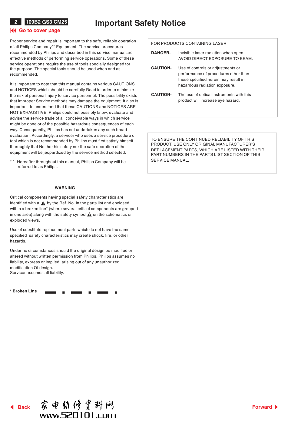
FOR PRODUCTS CONTAINING LASER :
Invisible laser radiation when open.
AVOID DIRECT EXPOSURE TO BEAM.
Use of controls or adjustments or
performance of procedures other than
those specified herein may result in
hazardous radiation exposure.
The use of optical instruments with this
product will increase eye hazard.
DANGER-
CAUTION-
CAUTION-
TO ENSURE THE CONTINUED RELIABILITY OF THIS
PRODUCT, USE ONLY ORIGINAL MANUFACTURER'S
REPLACEMENT PARTS, WHICH ARE LISTED WITH THEIR
PART NUMBERS IN THE PARTS LIST SECTION OF THIS
SERVICE MANUAL.
2
109B2 GS3 CM25
� Go to cover page
Forward
Back
109B2 GS3 CM25
3
CRT
Scanning
Video
Size and deflection
: 19" inch / 46 cm; 90 deflection
angle
Dot pitch /Grille pitch
: 0.25 mm
Horizontal pitch
: 0.21 mm
Tube type
: Shadow mask, Real Flat, high
contrast, anti-glare, anti-static,
anti-reflection, light transmission
44%
Phosphor
: P22
Recommended display area
: 14.0" x 10.4" / 355 x 265 mm
Maximum display area
: 14.4" x 10.8" /365 x 274 mm
Horizontal scanning
: 30 - 97 KHz
Vertical scanning
: 50 - 160 Hz
Input impedance
:
- Video
: 75 ohms
- Sync
: 2.2 K ohms
Input signal levels
: 0.7 Vpp
Sync input signal
: Separate sync
Composite sync
Sync polarities
: Positive and negative
�
Technical Specifications
Pin Assignment
Technical Data
1
Red video input
2
Green video input
3
Blue video input
4
Identical output - connected to pin 10
5
6
Red video ground
7
8
Blue video ground
9
No pin
10
Logic ground
11
Identical output - connected to pin 10
12
Serial data line (SDA)
13
H. Sync / H + V
14
V. Sync (VCLK for DDC)
15
Data clock line (SCL)
Pin No.
Assignment
Ground
Green video ground
White Color Temperature
Chromaticity CIE coordinates
:
at 9300 K degrees
: x = 0.283 / y = 0.297
at 6500 K degrees
: x = 0.313 / y = 0.329
at 5500 K degrees
: x = 0.332 / y = 0.347
Physical Characteristics
Dimensions
: 17.3" x 17.5" x 17.6" /
440 x 446 x 448 mm (including base)
440 x 410 x 448 mm (excluding
base)
Weight :
: 21.2 kg
Power supply
: 90- 264 VAC, 50/60Hz
Temperature (operating)
: 0 C to 40 C / 32
Relative humidity
: 5% to 95%
*
Resolution 1280 x 1024, standard size, contrast max., brightness
50%, 9300 K, full white pattern.
** These information are subject to change without notice.
�
�
�
�
�
�
�
�
�
F to 104 F
Temperature (storage)
: -25 C to 65 C / -13 F to 149 F
1
10
6
11
15
5
� Go to cover page
Automatic Power Saving
If you have VESA's DPMS compliance display card or software installed
in your PC, the monitor can automatically reduce its power consumption
when not in use. And if an input from a keyboard, mouse or other input
device is detected, the monitor will automatically "wake up". The
following table shows the power consumption and signaling of this
automatic power saving feature:
Power Management Definition
VESA's
Video
H-sync
V-sync
Power
Power
LED
Mode
Used
Saving
color
ON
Active
Yes
Yes
< 100W
0%
Green
< 10W
90%
Yellow
< 3W
97%
Amber
< 10W
90%
Yellow
Stand-by
Blanked
No
Yes
Suspend
Blanked
Yes
No
OFF
Blanked
No
No
This monitor is ENERGY STAR -compliant. As an ENERGY STAR
Partner, PHILIPS has determined that this product meets the ENERGY
STAR guidelines for energy efficiency.
�
�
�
Forward
Back
4
109B2 GS3 CM25
Go to cover page
Forward
Back
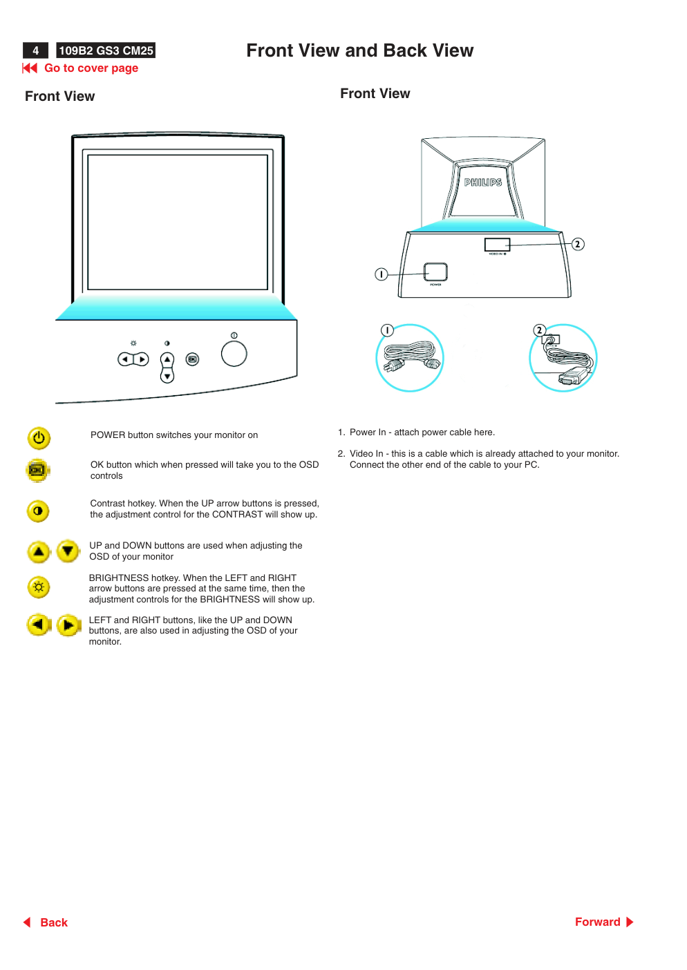
Front View and Back View
Front View
Front View
UP and DOWN buttons are used when adjusting the
OSD of your monitor
LEFT and RIGHT buttons, like the UP and DOWN
buttons, are also used in adjusting the OSD of your
monitor.
BRIGHTNESS hotkey. When the LEFT and RIGHT
arrow buttons are pressed at the same time, then the
adjustment controls for the BRIGHTNESS will show up.
Contrast hotkey. When the UP arrow buttons is pressed,
the adjustment control for the CONTRAST will show up.
OK button which when pressed will take you to the OSD
controls
POWER button switches your monitor on
1. Power In - attach power cable here.
2. Video In - this is a cable which is already attached to your monitor.
Connect the other end of the cable to your PC.
5
109B2 GS3 CM25
Go to cover page
Forward
Back
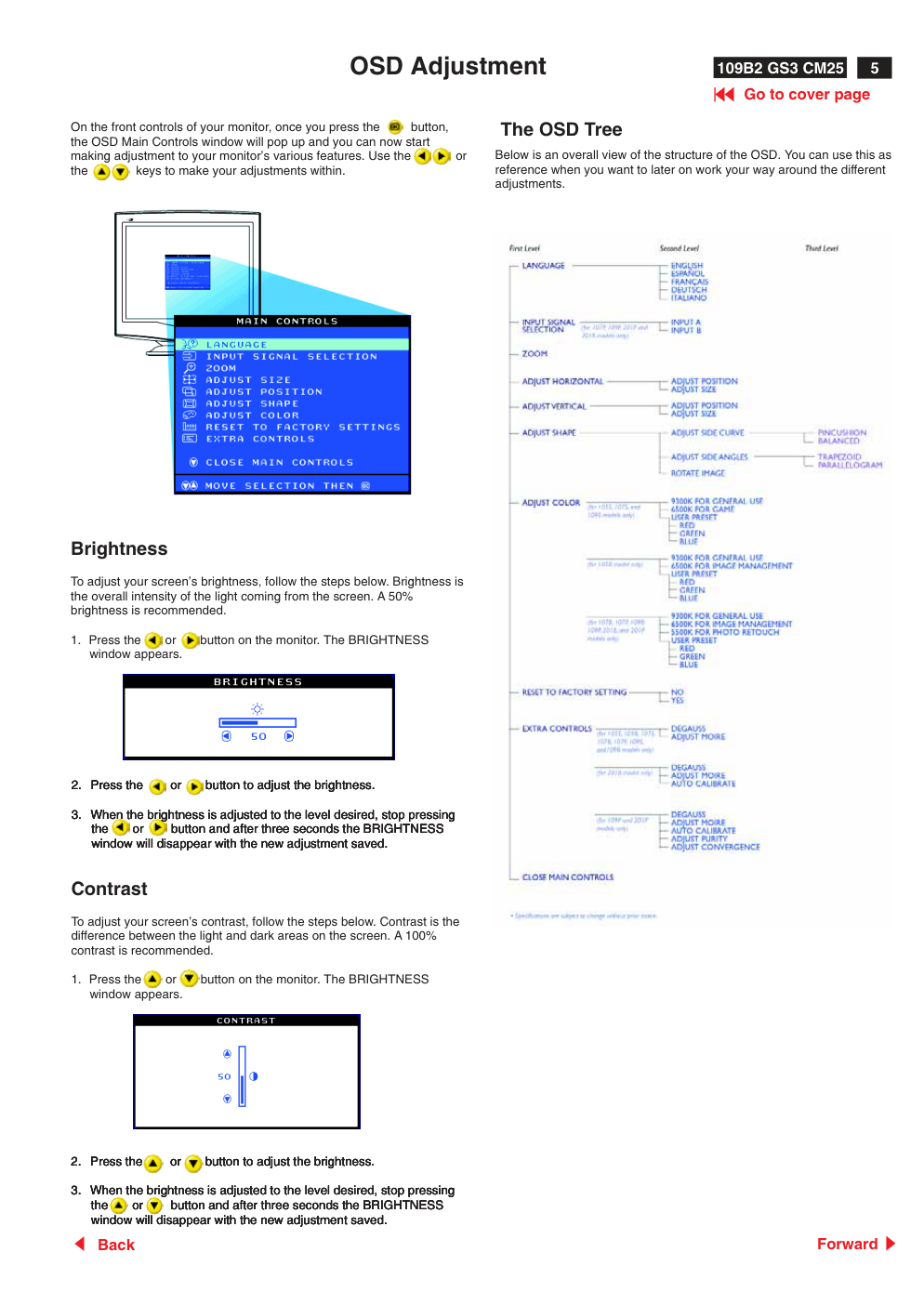
OSD Adjustment
The OSD Tree
On the front controls of your monitor, once you press the
button,
the OSD Main Controls window will pop up and you can now start
making adjustment to your monitor's various features. Use the
or
the
keys to make your adjustments within.
Brightness
1. Press the
or
button on the monitor. The BRIGHTNESS
window appears.
To adjust your screen's brightness, follow the steps below. Brightness is
the overall intensity of the light coming from the screen. A 50%
brightness is recommended.
Contrast
1. Press the
or
button on the monitor. The BRIGHTNESS
window appears.
To adjust your screen's contrast, follow the steps below. Contrast is the
difference between the light and dark areas on the screen. A 100%
contrast is recommended.
2. Press the
or
button to adjust the brightness.
3. When the brightness is adjusted to the level desired, stop pressing
the
or
button and after three seconds the BRIGHTNESS
window will disappear with the new adjustment saved.
2. Press the
or
button to adjust the brightness.
3. When the brightness is adjusted to the level desired, stop pressing
the
or
button and after three seconds the BRIGHTNESS
window will disappear with the new adjustment saved.
2. Press the
or
button to adjust the brightness.
3. When the brightness is adjusted to the level desired, stop pressing
the
or
button and after three seconds the BRIGHTNESS
window will disappear with the new adjustment saved.
2. Press the
or
button to adjust the brightness.
3. When the brightness is adjusted to the level desired, stop pressing
the
or
button and after three seconds the BRIGHTNESS
window will disappear with the new adjustment saved.
2. Press the
or
button to adjust the brightness.
3. When the brightness is adjusted to the level desired, stop pressing
the
or
button and after three seconds the BRIGHTNESS
window will disappear with the new adjustment saved.
2. Press the
or
button to adjust the brightness.
3. When the brightness is adjusted to the level desired, stop pressing
the
or
button and after three seconds the BRIGHTNESS
window will disappear with the new adjustment saved.
2. Press the
or
button to adjust the brightness.
3. When the brightness is adjusted to the level desired, stop pressing
the
or
button and after three seconds the BRIGHTNESS
window will disappear with the new adjustment saved.
2. Press the
or
button to adjust the brightness.
3. When the brightness is adjusted to the level desired, stop pressing
the
or
button and after three seconds the BRIGHTNESS
window will disappear with the new adjustment saved.
Below is an overall view of the structure of the OSD. You can use this as
reference when you want to later on work your way around the different
adjustments.
6
109B2 GS3 CM25
Go to cover page
Forward
Back
OSD Lock Function & Service Mode
To unlock (enable) OSD function:
- Press OSD button "
" for over 10 seconds again to unlock the
OSD function.
Release it, then OSD comes on the screen as below.
To lock (disable) OSD function:
- Press OSD button "
" for over 15 seconds to lock the OSD function.
Release it, then OSD comes on the screen as below.
ATTENTION
CONTROL MENU IS LOCKED
Disable/Enable all the WARNING SIGNAL
NO SIGNAL INPUT
To enable all the WARNING SIGNAL :
- After disconnect the Interface cable of the monitor, then Monitor is
powered ON.
- If it is successful, the signal "
" comes on the screen
again later.
Access Service mode (burn in mode) :
Access Service Mode & Burn in mode
Firstly, get into Factory Adjustment Mode.
Push LEFT
& RIGHT
buttons at the same time for
over 15 seconds and release them.
The factory message appears at the bottom of the
main OSD menu. (for example : 109B2 V1.52 20000619;
00115 is M.T.B.F. in HOUR unit)
SERVICE MODE
SERIAL NO: TY 123456
HOURS : 00021
FACTORY VER 1.01 990706
109B2 V1.52 20000619
00115
NO SIGNAL INPUT
To disable all the WARNING SIGNAL :
- Disconnect the Interface cable of the monitor (Monitor is ON.).
- Press OSD button "
" for over 15 seconds to disable all the
WARNING SIGNAL. Then release the "OSD" button.
- If it is successful, then the signal "
"disappeared to
enter power saving-off mode.
- Disconnect the Interface cable of the monitor.
- Push LEFT
& RIGHT
buttons at the same time, then power
ON.
- If it is successful, the signal "
"
comes on the screen later.
(Background is white.).
- Reconnect the interface cable to PC, then the "burn in MODE"
disappear.
Exit "burn in MODE" :
109B2 GS3 CM25
7
Warning and Notes
Fig.1
V
Warnings
1.
Safety regulations require that the unit should be returned
in its original condition and that components identical to
the original components are used. The safety components
are indicated by the symbol
.
2.
In order to prevent damage to ICs and transistors, all
high-voltage flash-overs must be avoided. In order to
prevent damage to the picture tube, the method shown
in Fig. 1 should be used to discharge the picture tube.
Use a high-voltage probe and a multimeter (position DC-V).
Discharge until the meter reading is 0 V (after approximately
30 seconds).
3.
ESD
All ICs and many other semiconductors are sensitive to
electrostatic discharges (ESD). Careless handling during
repair can drastically shorten their life. Make sure that
during repair you are connected by a pulse band with
resistance to the same potential as the ground of the unit.
Keep components and tools also at this same potential.
4.
When repairing a unit, always connect it to the AC Power
voltage via an isolating transformer.
5.
Be careful when taking measurements in the high-voltage
section and on the picture tube panel.
6.
It is recommended that saferty goggles be worn when
replacing the picture tube.
7.
When making adjustments,use plastic rather than metal tools.
This will prevent any short-circuit or the danger of a
circuit becoming unstable.
8.
Never replace modules or other components while the
unit is switched on.
9.
Together with the defleciton unit, the picture tube is used
as an integrated unit. Adjustment of this unit during repair
is not recommended.
10. After repair, the wiring should be fastened in place with
the cable clamps.
11. All units that are returned for service or repair must pass
the original manufactures safety tests.
Notes
1.
The direct voltages and waveforms are average voltages.
They have been measured using the Service test software
and under the following conditions :
-
Mode : 1024 * 768 (56.5kHz / 70Hz)
-
Signal pattern : grey scale
-
Adjust brightness and contrast control for the
mechanical mid-position (click position)
2.
The picture tube panel has printed spark gaps.
Each spark gap is connected between an electrode of the
picture tube and the Aquadag coating.
3.
The semiconductors indicated in the circuit diagram(s)
and in the parts lists are completely interchangeable per
position with the semiconductors in the unit, irrespective
of the type indication on these semiconductors.
� Go to cover page
Forward
Back
Mechanical Instructions
8
109B2 GS3 CM25
Fig. 5
Fig. 4
Fig. 3
Fig. 6
Fig. 8
Fig. 2
Fig. 7
screw
0. Location of the panel
1. General
0.1 Main panel (1155)
0.2 Video panel (1157)
To be able to perform measurements and repairs on the "circuit
boards", the monitor should be placed in Service Position (fig. 1) first:
There are 2 screws in the lid [1 screw are at the right side of the
monitor, the other 1 screw are at the left side of the monitor],to fix the
front cabinet and back cover of the monitor.
Step 1: To open the lid at the right-upper side and 1
right-
downer side of the monitor.(FIG.3)
Step 2: To open the lid at the left-upper side and
left-
downer side of the monitor.(FIG.4)
Step 3: To remove the backcover, you can see FIG.5
Step 4: To remove the16 screws on the metal shield, and remove the
metal shield, you can see FIG.6.
- After remove the back cover & metal shield, you can see the inside
of the monitor as Fig. 6.
- To remove 5 screws for service position as Fig. 6 to Fig. 8.
- Including remove bottom plate screw, then slide out chassis board
and disconnect metal shield.
- After remove the metal frame (Fig. 5), to remove the metal shield on
rear side of Video panel for measurement.
After remove the metal frame.
- To cut out cable tie and disconnect "video panel"
- To disconnect EHT cable
- To disconnect ground wire(1703) of video board.
- To disconnect M1802(6pin) to control panel.
- To disconnect M1401(4pin) yoke connector.
- To disconnect M1603(2pin) degaussing coil
- To slide out Main panel as Fig. 1.
To get service position as Fig. 1 through Fig. 2 to Fig. 8.
After the service position was obtained, all the panel's copper track
side could be accessed.
How to remove the back cover of monitor :
screw in
1screw in
Chassis :
Video panel :
Main panel :
Service position :
2. Repair instructions
Service Position
Fig. 1
1157
lids
screws
1155
Go to cover page
Forward
Back
9
109B2 GS3 CM25
Go to cover page
Forward
Back
Safety Test Requirements
2.2.1 The test with AC voltage is only for production purpose,
Service center shall use DC voltage.
2.2.2 The minimum test duration for Quality Control Inspector
must be 1 minute. No breakdown during the test.
2.2.3 The test voltage must be maintained within the specified
voltage + 5%.
2.2.4 The grounding blade or pin of mains plug must be
conducted with accessible metal parts.
All units that are returned for service or repair must pass the original
manufactures safety tests. Safety testing requires both
and
testing.
Hi-pot
Ground Continuity
HI-POT TEST INSTRUCTION
1. Application requirements
2. Test method
1.1
All mains operated products must pass the Hi-Pot test as
described in this instruction.
1.2
This test must be performed again after the covers have
been refitted following the repair, inspection or modification
of the product.
2.1
Connecting conditions
2.1.1 The test specified must be applied between the parallel-
blade plug of the mainscord and all accessible metal
parts of the product.
2.1.2 Before carrying out the test, reliable conductive
connections must be ensured and thereafter be
maintained throughout the test period.
2.1.3 The mains switch(es) must be in the "ON" position.
2.2
Test Requirements
All products should be HiPot and Ground Continuity tested as follows:
Condition
HiPot Test for
HiPot Test for
Ground Continuity
products where
products where
Test requirement
the mains input
the mains input is
range is Full
110V AC(USA
range(or 220V
type)
AC)
Test
2820VDC
1700VDC
Test current:
voltage
(2000VAC)
(1200VAC)
25A,AC
Test time:
Test time
3 seconds
1 second
3 seconds(min.)
(min.)
Resistance
required:
Trip
set at 100 uA
5 mA
<=0.09+R ohm,
current
for Max.
R is the
(Tester)
limitation; set
resistance of
at 0.1 uA for
the mains cord.
Min. limitation
Ramp
set at 2
time
seconds
(Tester)
3. Equipments and Connection
4. Recording
3.1
Equipments
For example :
- ChenHwa 9032 PROGRAMMABLE AUTO SAFETY
TESTER
- ChenHwa 510B Digital Grounding Continuity Tester
- ChenHwa 901 (AC Hi-pot test), 902 (AC, DC Hi-pot test)
Withstanding Tester
3.2
Connection
Hipot and Ground Continuity testing records have to be kept for a period
of 10 years.
* Turn on the power switch of monitor before Hipot and
Ground Continuity testing.
Connect the "video cable"
or "grounding screw"
to the CLIP on your tester.
Video cable
(Rear view of monitor)
Connect the power cord
to the monitor.
Grounding screw
Power outlet
(ChenHwa 9032 tester)
Clip
Clip
10
109B2 GS3 CM25
Go to cover page
Forward
Back
Wiring Diagram
8801
8601
10
1113
3
1401
1603
1
1713
9
1714
10
1301
13
1
TO YOKE
1712
RED
GRAY
WHITE
TO HVG
RED
GRAY
WHITE
88911
1605
1
1
2
3
DEGAUSSING COIL
EARTH WIRE
CONTROL PCB ASSY
MAIN PCB ASSY
YOKE
VIDEO PCB ASSY
1802
TO POSITION 1714 OF VIDEO PCB
1713
TO INSERT CRT NECK
(DETAIL POSITION REFER
SHEET 132 PHOTO)
TO INSERT CRT NECK
(DETAIL POSITION REFER
SHEET 132 PHOTO )
TO PLUG IN BOTTOM PLATE - B
TO PLUG IN BOTTOM PLATE - A
TO PLUG IN BOTTOM PLATE - C
BOTTOM PLATE
A
B
C
11
109B2 GS3 CM25
Go to cover page
Forward
Back
DDC Data
**********************************************************************
EDID log file for HTC tube
**********************************************************************
Vendor/Product Identification
ID Manufacturer Name
: PHL
ID Product Code
: E007 (HEX.)
ID Serial Number
: 12345 (DEC.)
Week of Manufacture
: 28
Year of Manufacture
: 2000
EDID Version, Revision
Version
: 1
Revision
: 2
Basic Display Parameters/Features
Video Input Definition
: Analog Video Input
0.700V/0.000V (0.70Vpp)
without Blank-to-Black Setup
Separate Sync
without Composite Sync
without Sync on Green
no Serration required
Maximum H Image Size
: 36
Maximum V Image Size
: 27
Display Transfer Characteristic: 2.76
(gamma)
Feature Support (DPMS)
: Standby
Suspend
Active Off
Display Type
: RGB color display
Color Characteristics
Red
X coordinate
: 0.625
Red
Y coordinate
: 0.34
Green X coordinate
: 0.285
Green Y coordinate
: 0.605
Blue X coordinate
: 0.15
Blue Y coordinate
: 0.065
White X coordinate
: 0.283
White Y coordinate
: 0.297
Established Timings
Established Timings I
: 720 x 400 @70Hz (IBM,VGA)
640 x 480 @60Hz (IBM,VGA)
640 x 480 @72Hz (VESA)
640 x 480 @75Hz (VESA)
800 x 600 @60Hz (VESA)
Established Timings II
: 800 x 600 @72Hz (VESA)
800 x 600 @75Hz (VESA)
832 x 624 @75Hz (Apple,Mac II)
1024 x 768 @60Hz (VESA)
1024 x 768 @70Hz (VESA)
1024 x 768 @75Hz (VESA)
1280 x 1024 @75Hz (VESA)
Manufacturer's timings
: 1152 x 870 @75Hz (Apple,Mac II)
Standard Timing Identification #1
Horizontal active pixels
: 640
Aspect Ratio
: 4:3
Refresh Rate
: 85
Standard Timing Identification #2
Horizontal active pixels
: 800
Aspect Ratio
: 4:3
Refresh Rate
: 85
Standard Timing Identification #3
Horizontal active pixels
: 1024
Aspect Ratio
: 4:3
Refresh Rate
: 85
Standard Timing Identification #4
Horizontal active pixels
: 1280
Aspect Ratio
: 5:4
Refresh Rate
: 85
Standard Timing Identification #5
Horizontal active pixels
: 1600
Aspect Ratio
: 4:3
Refresh Rate
: 75
Standard Timing Identification #6
Horizontal active pixels
: 1920
Aspect Ratio
: 4:3
Refresh Rate
: 60
Detailed Timing #1
Pixel Clock (Mhz)
: 202.5
H Active (pixels)
: 1600
H Blanking (pixels)
: 560
V Active (lines)
: 1200
V Blanking (lines)
: 50
H Sync Offset (F Porch) (pixels)
: 64
H Sync Pulse Width (pixels)
: 192
V Sync Offset (F Porch) (lines)
: 1
V Sync Pulse Width (lines)
: 3
H Image Size (mm)
: 360
V Image Size (mm)
: 270
H Border (pixels)
: 0
V Border (lines)
: 0
Flags
: Non-interlaced
: Normal Display, No stereo
: Digital Separate sync.
: Positive Vertical Sync.
: Positive Horizontal Sync.
Monitor Descriptor #2
Serial Number
: TY 123456
Monitor Descriptor #3
Monitor Name
: PHILIPS 109B2
Monitor Descriptor #4
Monitor Range Limits
Min. Vt rate Hz
: 50
Max. Vt rate Hz
: 160
Min. Horiz. rate kHz
: 30
Max. Horiz. rate kHz
: 97
Max. Supported Pixel
: Not specified
Extension Flag
: 0
Check sum
: A5 (HEX.)
**********************************************************************
EDID data (128 bytes)
**********************************************************************
0: 00
1: ff
2: ff
3: ff
4: ff
5: ff
6: ff
7: 00
8: 41
9: 0c
10: 07
11: e0
12: 39
13: 30
14: 00
15: 00
16: 1c
17: 0a
18: 01
19: 02
20: 68
21: 24
22: 1b
23: b0
24: e8
25: 00
26: b8
27: a0
28: 57
29: 49
30: 9b
31: 26
32: 10
33: 48
34: 4c
35: ad
36: ef
37: 80
38: 31
39: 59
40: 45
41: 59
42: 61
43: 59
44: 81
45: 99
46: a9
47: 4f
48: d1
49: 40
50: 01
51: 01
52: 01
53: 01
54: 1a
55: 4f
56: 40
57: 30
58: 62
59: b0
60: 32
61: 40
62: 40
63: c0
64: 13
65: 00
66: 68
67: 0e
68: 11
69: 00
70: 00
71: 1e
72: 00
73: 00
74: 00
75: ff
76: 00
77: 20
78: 54
79: 59
80: 20
81: 20
82: 31
83: 32
84: 33
85: 34
86: 35
87: 36
88: 0a
89: 20
90: 00
91: 00
92: 00
93: fc
94: 00
95: 50
96: 48
97: 49
98: 4c
99: 49
100: 50
101: 53 102: 20 103: 31
104: 30 105: 39 106: 42 107: 32 108: 00
109: 00 110: 00 111: fd
112: 00 113: 32 114: a0 115: 1e
116: 61
117: ff
118: 00 119: 0a
120: 20 121: 20 122: 20 123: 20 124: 20
125: 20 126: 00 127: a5
12
109B2 GS3 CM25
Go to cover page
Forward
Back
DDC Instructions
1. General
3. Pin assignment
Fig. 2 Alignment Kits
To Monitor
DC 8V~12V
Video Card
Video Card
To Printer
Power indicator
A. 15-pin D-Sub Connector
DDC Data Re-programming
In case the main EEPROM with
which store all factory
settings were replaced because a defect,repaired monitor’ the serial
numbers have to be re-programmed.
It is advised to re-soldered the main EEPROM
from
the old board onto the new board if circuit board have been replaced, in
this case the DDC data does not need to be re-programmed.
Additional information
Additional information about DDC (Display Data Channel) may be
obtained from Video Electronics Standards Association (VESA).
Extended Display Identification Data(EDID) information may be also
obtained from VESA.
DDC EDID structure
For the monitor
: Standard Version
3.0
Structure Version
1.2
1.
An i486 (or above) personal computer or compatible.
2.
Microsoft operation system Windows 95/98.
4.
Software DDC Alignment kits (4822 310 11184) shown as Fig. 2.
The kit contents: a. Alignment box x1
b. Printer cable
x1
c. D-Sub cable
x1
Note: The EDID301.EXE (Release Version 1.54, 2000.04.25)is a
windows-based program, which cannot be run in MS-DOS.
Software DDC
with Software DDC
3.
EDID301.EXE program (3138 106 10103) shown as Fig. 1
2. System and equipment requirements
Diskette with EDID301.EXE
EDID301.EXE
Figure 1
Ver:1.54
The 15-pin D-sub connector (male) of the signal cable
on the 3rd row for DDC feature :
1
Red video input
2
Green video input
3
Blue video input
4
Identical output - connected to pin 10
5
6
Red video ground
7
8
Blue video ground
9
No pin
10
Logic ground
11
Identical output - connected to pin 10
12
Serial data line (SDA)
13
H. Sync / H + V
14
V. Sync (VCLK for DDC)
15
Data clock line (SCL)
Pin No.
Assignment
Ground
Green video ground
1
10
6
11
15
5
13
109B2 GS3 CM25
Go to cover page
Forward
Back
DDC Instructions (Continued)
4. Configuration and procedure
Following descirptions are the connection and procedure for Software
DDC, the main EEPROM can be re-programmed along with Software
DDC by enabling “factory memory data write” function on the DDC
program (EDID301.EXE).
5. DDC re-programming instructions
Start on DDC program
Start Microsoft Windows.
1. Insert the disk containing EDID301.EXE program into floppy disk
drive.
2. Click
, choose Run at start menu of Windows 95/98.
4. At the submenu, type the letter of your computer's floppy disk drive
followed by :EDID301 (for example, A:\EDID301, as shown in Fig. 5).
Fig. 5
Initialize alignment box
In order to avoid that monitor entering power saving mode due to sync
will cut off by alignment box, it is necessary to initialize alignment box
before running programming software (EDID301.EXE). Following steps
show you the procedures and connection.
Step 1: Supply 8~12V DC power source to the Alignment box by
plugging a DC power cord or using batteries.
Step 2: Connecting printer cable and video cable of monitor as Fig. A
Step 3: Run the EDID301.EXE program until the main menu appears.
This is for initialize alignment box.
~~
PC
To video card
To printer port (LTP1)
DC Power
8~12 V
Fig. 3
Printer
Port
Re-programming Software DDC
Step 1: After initialize alignment box, connecting all cables and box as
Fig. 3
Step 2: Follow the steps on DDC re-programming instructions to staring
re-programming.
To
Monitor
To PC
Rear view of the monitor
Video cable
~~
PC
To printer port (LTP1)
DC Power
8~12 V
Fig. A
Printer
Port
To video card
To
Monitor
To PC
Video cable
Rear view of the monitor
A:\edid301�
14
109B2 GS3 CM25
Go to cover page
Forward
Back
DDC Instructions (Continued)
Loading DDC data from monitor
1.
Click
icon on the tools bar to bring up the Configuration Setup
windows as Fig.7
2.
Select the DDC2B as the communication channel.
3.
Enable Factory memory data write function and fill in page address
“FA” to the block.
4..
Click
button to confirm your selection.
Note: The Factory memory data write function will allow EDID301 to
rewrite the serial numbers of Software DDC data in main
EEPROM.
5. Click
button. The main menu appears (as shown on Fig. 6).
Fig. 6
Note:
If the connection is improper, you will see the following error
message before entering the main menu. Meanwhile, the
(read EDID) function will be disable. At this time, please make
sure all cables are connected correctly and fixedly, and the
procedure has been performed properly.
4.
Click
icon to read DDC EDID data from monitor. The EDID
codes will display on screen as following. (The EDID codes are
dependent on the model.)
Command bar
Tools bar
Status bar
Fig. 7
Modify DDC data (Serial No.)
1.
Click
icon on the tool bar.
2.
Click
till the Step 7 of 9 window appears.
3.
Type the new Serial No. (for example, TY 123456).
4.
Click
till the last step window appears, then click
to
exit the Step window.
Note:
During the loading, EDID301 will verify the EDID data which just
loaded from monitor before proceed any further function, once
the data structure of EDID can not be recognized, the following
error message will appear on the screen (Fig. 8). Please confirm
following steps to avoid this message.
1. The data structure of EDID was incorrect.
2. Software DDC Data that you are trying to load data is empty.
3. Wrong communication channel has set at configuration setup
windows.
4. Cables loosed or poor contact of connection.
5. Software DDC only is disable.
Fig. 8
1
F0
15
109B2 GS3 CM25
Go to cover page
Forward
Back
DDC Instructions (Continued)
Load DDC data from file
1.
Click
from the tools bar.
2.
Select the file you want to open.
3.
Click .
Button.
Exit DDC program
1.
Click file command on the command bar then select Exit.
Write DDC data to monitor
1.
Click
icon from the tools bar to starting rewrite DDC data.
2.
Click
for confirmation.
Save DDC data as a file
Sometimes, you maybe need to save DDC data as a text file for using
on other DDC chip. To save DDC data, follow the steps below:
1.
Click
icon on the tools bar and type a file name you like. The
file format is ddc type which can be open by Microsoft WordPad.
2.
Click
button.
Definition of Serial Number
T Y 0 0 0 0 2 8 0 0 0 0 0 1
Serial Number (U.S.A: 8 digit)
Week
Year
TY Code
TY----Chungli
CX----Dong Guan
HD----Hungary
BZ----Suzhou
(Others regions: 6 digit)
4.
Now you can re-programming DDC data which you just loaded
from a file, please be confirmed that model and serial number are
correct and match with the monitor you are trying to re-write.
1
1
16
109B2 GS3 CM25
Go to cover page
Forward
Back
Electrical Instructions
0. General
1. B+ supply voltage (3165) 79Vdc
2. High-voltage EHT (3587)
When carry-out the electrical settings in many cases a video
signal must be applied to the monitor. A computer with :
- ATI GPT-1600 (4822 397 10065), Mach 64 (up to 107kHz)
are used as the video signal source. The signal patterns
are selected from the "service test software" package, see
user guide 4822 727 21046 (GPT-1600).
The measurements for AC waveform and DC figure is based
on 640 x 480 31.5 kHz/60 Hz resolution mode with test
pattern "gray scale".
Power input: 110V AC
- Apply a video signal in the 1024 x 768 with 68.7 kHz/85Hz
mode.
- Select the "cross-hatch" pattern.
- Set the brightness control and the contrast control to the
minimum
position.
- Pre-set trimming potentiometer R3165(B+) and
R3587(EHT) in mid-position.
- Set Vg2 (screen) to fully Counter-clockwise (zero
beamcurrent).
- Connect a dc voltmeter between the joint of C2152 and
ground (common ground).
- Set the B+ trimming potentiometer 3165 so that the reading
on the dc voltmeter is 190.0 V +/- 0.5 Vdc.
- Apply a video signal in the 1024 x 768 with 68.7 kHz/85Hz
mode.
- Select the "cross-hatch" pattern.
- Set the brightness control and the contrast control to the
minimum position.
0.1 This monitor has 35 factory-preset modes as below:
z
0.2 With normal VGA card:
If not using the ATI card during repair or alignment, The
service engineer also can use this service test software
adapting with normal standard VGA adaptor and using
standard VGA mode 640 x 480, 31.5 kHz/60 Hz (only) as
signal source.
0.3 AC/DC Measurement:
640 x 350 37.9 kHz/85 Hz
1152 x 870 68.7 kHz/75 Hz
640 x 400 31.5 kHz/70 Hz
1152 x 900 71.8 kHz/76 Hz
640 x 480 31.5 kHz/60 Hz
1280 x 960 60.0 kHz/60 Hz
640 x 480 37.9 kHz/72 Hz
1280 x 960 85.9 kHz/85 Hz
640 x 480 37.5 kHz/75 Hz
1280 x 1024 63.9 kHz/60Hz
640 x 480 43.3 kHz/85 Hz
1280 x 1024 79.9 kHz/75 Hz
640 x 480 50.6 kHz/100 Hz
1280 x 1024 91.1 kHz/85 Hz
0 x 400 31.5 kHz/70 Hz
1600 x 1200 75.0 kHz/60 Hz
720 x 400 37.9 kHz/85 Hz
1600 x 1200 81.3 kHz/65 Hz
800 x 600 37.9 kHz/60 Hz
1600 x 1200 87.5 kHz/70 Hz
800 x 600 48.1 kHz/72 Hz
1600 x 1200 93.8 kHz/75 Hz
800 x 600 46.9 kHz/75 Hz
1792 x 1344 83.6 kHz/60 Hz
800 x 600 53.7 kHz/85 Hz
1856 x 1392 86.3 kHz/60 Hz
800 x 600 63.9 kHz/100 Hz
1920 x 1440 90.0 kHz/60 H
832 x 624 49.7 kHz/75 Hz
1024 x 768 48.4 kHz/60 Hz
1024 x 768 56.5 kHz/70 Hz
1024 x 768 60.0 kHz/75 Hz
1024 x 768 68.7 kHz/85 Hz
1152 x 864 67.5 kHz/75 Hz
1152 x 864 77.1 kHz/85 Hz
72
- Connect a "high-voltage voltmeter" between the high-
voltage connection of the picture tube and earth.
- Turn on the power.
- Set the EHT trimming potentiometer R3587 so that the
"high-
voltage voltmeter" reads 26.5 KV +/- 0.5 KV .
- Turn off the power.
- Remove the "high-voltage voltmeter" from the picture tube.
- Turn on the power again.
3. Monitor the following auxiliary voltages.
SOURCE ACROSS C2152 + 190.0V +/- 1.0VDC.
SOURCE ACROSS C2154 +
79.0V +/- 1.0VDC.
SOURCE ACROSS C2156
-
6.3V +/- 0.3VDC.
SOURCE ACROSS C2160 +
13.5V +/- 0.5VDC.
SOURCE ACROSS C2157 -
13.5V +/- 0.5VDC.
4. General conditions for alignment
4.1 During all alignments, supply a distortion free AC mains
voltage to set via an isolating transformer with low internal
impedance.
4.2 Align in pre-warmed condition, at least 30 minutes warm-
up with nominal picture brightness.
4.3 Purity, geometry and subsequent alignments should be
carried out in magnetic cage with correct magnetic field.
Northern hemisphere : H=0, V=430+/-50 mG, Z=0
Southern hemisphere : H=0, V=-520+/-50 mG, Z=0
4.4 All voltages are to be measured or applied with respect to
ground.
Note: Do not use heatsink as ground.
4.5 Adjust function controls "
" to center position except
for contrast control which should be set to MAX.
5. To access factory mode:
- Turn off monitor (don't turn off PC)
- Press "
" and "
" simultaneously on the front
control panel, then press "
",wait till the OSD menu
with characters " factory mode (below OSD menu)" come
on the screen of monitor.
109B2 V1.52 20000619
00115
- If OSD menu disappears on the screen of monitor, press
"
" again (anytime), then the OSD menu comes on the
screen again.
- using "
" : to select OSD menu.
: to increase or decrease the setting.
- Using "
" to confirm the selection.
17
109B2 GS3 CM25
Electrical Instructions (Continued)
.
7.1 Connect the video input, set brightness control at 50%
and contrast at minimum position (OSD), Vg2 at Minimum
(counter clockwise, and ABL (OSD) at 50% position.
Slowly increase Vg2 voltage until light output is at
0.1 Ft-L +/- 0.01Ft-L (Y=0.1 Ft-L, on the screen of CA-
100).
7.2 (The screen of monitor is dark now)
: Press "
" to show the OSD menu as shown in Fig.
2.1.
: Select the character "FACTORY MODE" to access the
R/G/B adjustment as shown in Fig. 2.2 and Fig. 2.3.
: Adjust the cutoff of R/G/B to get 9300K
(x=0.283 +/- 0.015, y=0.297 +/- 0.015), and brightness
output at 0.07 +/- 0.01 Ft-L (Y=0.07Ft-L).
7.3 : Press "
" to set contrast at maximum (100%).
: Adjust gain of R/G/B to get 9300K
(x=0.283 +/- 0.015, y=0.297 +/-0.015, don't care about
the Y value)
7.4 Apply a small white square 10 x 10 cm pattern, brightness
set to center (50%), and contrast at maximum (100%),
adjust Sub-contrast control (OSD) to reach 44 +/- 1 Ft-L.
7.5 Apply full white pattern at 9300K, adjust ABL (OSD) to
reach 30+/- 1 Ft-L (contrast at maximum 100%,
brightness at center 50%).
LF
: LightFrame
BIAS R G B : R(red) G(green) B(blue) cutoff
GAIN R G B : R(red) G(green) B(blue) gain
V FOCUS : Vertical Focus
H FOCUS : Horizontal Focus
VLIN BAL : Vertical Linearity Balance
USER
: Horizontal size range
RASTER H: Horizontal raster Shift
RASTER V: Vertical raster Shift
HLIN
: Horizontal Linearity
V LIN
: Vertical Linearity
SUB
: Zoom Control range
SUB
: Sub Contrast
V OFFSET : Vertical offset
V GAIN
: Vertical Gain
ABL
: Auto Beam Limit
T CORNER: Corner Correctionof TOP
B CORNER: Corner Correctionof BOTTOM
6 To leave factory mode
* After alignment of factory mode, turn off monitor (if you do
not turn off monitor, the OSD menu is always at the factory
mode), then turn on monitor again (at this moment, the
OSD menu goes back to user mode).
TIMER
Set OSD display time.
5500 K
R cutoff = 40%, R gain = 55% (I C)
G cutoff = 40%, G gain = 55% (I C)
B cutoff = 40%,
B gain = 55% (I C)
2
2
2
2
2
2
2
2
2
�
7. Alignment of Vg2 cut-off point, white tracking (OSD
control)
Equipment : 1. Video Test Generator-801GC (Quantum
Data)
2. Color-analyzer (Minolta CA-100)
VG2 [(screen), at the bottom of the L.O.T.].
* Apply a video signal in the 1024 x 768 with 68.7 kHz/85 Hz
mode,
select the "full white pattern" (sizes 355 x 265 mm).
* Use color-analyzer (Minolta CA-100) to adjust cutoff and
white uniformity.
OSD R/G/B cut-off and R/G/B gain can be accessed, with
initial data:
9300 K
R cutoff = 40%, R gain = 65% (I C)
G cutoff = 40%, G gain = 65% (I C)
B cutoff = 40%,
B gain = 65% (I C)
6500 K
R cutoff = 40%, R gain = 55% (I C)
G cutoff = 40%, G gain = 55% (I C)
B cutoff = 40%,
B gain = 55% (I C)
Brightness = 50%, Sub-Contrast = 85%, ABL = 70% (I C)
Step 1: To select the character "FACTORY MODE" as shown
in Fig. 2.1, press "
" to access the OSD menu for
R/G/B gain & cutoff as shown in Fig. 2.2.
Step 2: Press "
" for function selection as shown in Fig
2.3.
Step 3: Use "
" to increase or decrease the value as
shown in Fig. 2.3.
�
�
2
After pressing "
" ,then Press "
"
2
Fig.2.1
Fig. 2.2
Fig. 2.3
9300 BIAS
R G B
GAIN R G B
6500 BIAS
R G B
GAIN R G B
5500 BIAS
R G B
GAIN R G B
FOCUS(H V) VLINBAL USER
RASTER(H V) LIN ( H V ) SUB
V(OFFSET GAIN)
SUB
CORNER(T B) ABL
LF(BRIGH SHARP)
LF(BRIGH SHARP)
EXIT
135
9300 BIAS
R G B
GAIN R G B
6500 BIAS
R G B
GAIN R G B
5500 BIAS
R G B
GAIN R G B
FOCUS(H V) VLINBAL USER
RASTER(H V) LIN ( H V ) SUB
V(OFFSET GAIN)
SUB
CORNER(T B) ABL
EXIT
135
109B2 V1.52 20000619
00115
Go to cover page
Forward
Back
18
109B2 GS3 CM25
Electrical Instructions (Continued)
9. Focus adjustment
10. Loading DDC code
: Apply a video signal in the 1600 x 1200 with 93.8 kHz/75
Hz mode
: Select " @
" pattern.
: Set the brightness at center (50%) and the contrast to 25
FL.
: Adjust focus potentiometers (top of L.O.T.) Focus 1 for
horizontal focus and Focus 2 for vertical focus so that the
picture at 2/3 of the diagonal lines (from center to four
corners) of the displayed screen is as sharp as possible.
The DDC HEX data should be written
into the DDC IC by EEPROM writer or EDID301.EXE
program and Software DDC Alignment Kit.
7.6 : Select the 6500K colour temperature as shown in Fig.
2.2.
: Adjust the R/G/B cutoff and R/G/B gain as shown in
procedure 7.2~7.3 to get
R/G/B cutoff
x= 0.313 +/- 0.015
y= 0.329 +/- 0.015
R/G/B gain
x= 0.313 +/- 0.015
y= 0.329 +/- 0.015
Y= 38 +/- 1 Ft-L
7.7 : Select the 5500K colour temperature as shown in Fig.
2.2.
: Adjust the R/G/B cutoff and R/G/B gain as shown in
procedure 7.2~7.3 to get
R/G/B cutoff
x= 0.332 +/- 0.015
y= 0.347 +/- 0.015
R/G/B gain
x= 0.332 +/- 0.015
y= 0.347 +/- 0.015
Y= 33 +/- 1 Ft-L
- Apply a video signal with cross-hatch pattern.
- Apply a video signal in the 1024 x 768 with 68.7 kHz/85 Hz
mode.
- Set brightness and contrast controls to their center positions
(OSD control).
8. Picture geometry setting (factory pre-set modes)
8.1 Horizontal geometry (OSD control)
- Adjust the H-width to 355 mm
- Adjust the H-phase to center position.
8.2 Vertical geometry (OSD control)
- Adjust vertical size to 265 mm
- Adjust V-phase to center position.
8.3 Trapezoid distortion (OSD control)
- Adjust the trapezoid to get optimal vertical lines.
8.4 Pincushion (OSD control)
- Adjust the pincushion to get optimal vertical line.
8.5 Parallelogram (OSD control)
- Adjust parallelogram so that vertical lines are vertical or
symmetrically about the center vertical axis.
8.6 Unbalance-pin (OSD control)
- Adjust the unbalance-pin so that that vertical border lines
are aligned symmetrically.
8.7 Rotation (OSD control)
- Adjust picture so that vertical tilt is less than +/- 0.5mm.
8.8 Top/Bottom corner(control)
- Adjust the top/bottom corner control to get optimum corner
geometry.
8.9 Store the preset results by selecting the "exit" (OSD
control).
8.10 Repeat the procedure 8.1 to 8.9 until all the preset
timings have been adjusted completely
Go to cover page
Forward
Back
19
109B2 GS3 CM25
Go to cover page
Forward
Back
Electrical Instructions (Continued)
CHARACTER
FOR FOCUS
IMAGE GEOMETRY
355 mm
265 mm
A, B < 2.0 mm
C, D < 2.0 mm
A
B
C
D
Item Resolution
Freq. V x H
Pixel rate(Mhz)
Remark
1
640x350
85(37.861k)
31.500
VESA
2
640x350
70(31.469k)
25.175
VGA
3
640x480
60(31.469k)
25.175
VGA
4
72.8(37.861k)
31.500
VESA
5
75(37.500k)
31.500
VESA
6
85(43.269k)
36.000
VESA
7
100.1(50.60k)
40.500
SNI
8
720x400
70(31.469k)
28.321
VGA
9
85(37.927k)
35.500
VESA
10
800x600
60.3(37.879k)
40.000
VESA
11
72.12(48.077k)
50.000
VESA
12
75(46.875k)
49.500
VESA
@13
85(53.674k)
56.250
VESA
14
100.1(63.90k)
67.500
SNI
15
832x624
74.6(49.725k)
57.280
MAC
16
1024x768
60(48.363k)
65.000
VESA
17
70(56.476k)
75.000
VESA
@18
75(60.000k)
78.750
VESA
@19
84.997(68.677k)
94.500
VESA
20
1152x864
75(67.500k)
108.000
VESA
21
85(77.100k)
121.500
VESA/P
22
1152x870
75(68.681k)
100.000
MAC
23
1152x900
76(71.800k)
108.000
SUN
24
1280x960
60(60.000k)
108.000
VESA
25
85(85.938k)
148.500
VESA
26
1280x1024
60(63.981k)
108.000
VESA
@27
75(79.976k)
135.000
VESA
@28
85(91.146k)
157.500
VESA
29
1600x1200
60(75.000k)
162.000
VESA
30
65(81.250k)
175.500
VESA
31
70(87.500k)
189.000
VESA
@32
75(93.750k)
202.500
VESA
33
1792x1344
60(83.640k)
204.750
VESA/P
34
1856x1392
60(86.333k)
218.250
VESA/P
35
1920x1440
60(90.000k)
234.000
VESA/P
20
109B2 GS3 CM25
1.
Purity adjustment
2.
Static convergence
- Make sure the monitor is not exposed to any
external magnetic field.
- Produce a full red pattern on the screen, adjust the
purity magnet rings on the PCM assy (on CRT) to
obtain a complete field of the color red. This is done
by moving the two tabs (2-pole) in such a manner
that they advance in an opposite direction but at
the same time to obtain the same angle between
the two tabs, which should be approximately 180
degree.
- Check by full green pattern and full blue pattern
again to observe their respective color purity.
Introduction
Slight deviation in the static convergence can be
corrected by using two permanent pairs of magnets
which are fitted around the neck of the CRT. These
are the 4-pole magnet and the 6-pole magnet.
The 4-pole magnet move the outermost electron
beams (R and B) parallel in the opposite direction
from the other. The 6-pole magnet moves the
outermost electron beam (R, B and G) parallel in the
opposite direction from the other.
The magnetic field of the above magnets do not affect
the center of the CRT neck.
Setting
- Before the static convergence setting can be made,
the monitor must be switched on for 30 minutes.
- The focus setting must be made correctly.
- Signal: 640 * 480, 31.5 kHz/60 Hz mode.
- Set the tabs of the 4-pole magnet in the neutral
position. This is when the tabs are opposite one
another. In this position the magnets do not affect the
deflection of the R and B electron beams.
- Set the tabs of the 6-pole magnet in the neutral
position. This is when the tabs are opposite one
another. In this position the magnets do not affect the
deflection of the R, B, and G electron beams.
- First set the 4-pole magnet optimally.
- Then set the 6-pole magnet optimally.
- If the convergence is not now optimal, then adjust to
the optimal setting with the 4-pole magnet and then with
the 6- Pole magnet again.
- Set the tabs of the 6-pole magnet in the neutral
position. This is when the tabs are opposite one
another. In this position the magnets do not affect the
deflection of the R, B, and G electron beams.
- First set the 4-pole magnet optimally.
- Then set the 6-pole magnet optimally.
- If the convergence is not now optimal, then adjust to
the optimal setting with the 4-pole magnet and then
with the 6- pole magnet again.
2-pole purity magnet
6-pole convergence magnet
4-pole convergence magnet
Deflection Yoke
4-pole
Beam motion producced by the
4-pole convergence magnet
S
S
N
N
B
G
R
S
S
N
N
B
G
R
Beam displacement
direction
Magnetic flux
lines
6-pole
Beam motion producced by the
6- pole convergence magnet
S
S
S
N
N
N
R
B
G
S
S
S
N
N
N
R
B
G
Go to cover page
Forward
Back
Electrical Instructions (Continued)
Block Diagram
21
109B2 GS3 CM25
Go to cover page
Forward
Back
H V
V H
H
V
H. freq. : 30 - 97KHz
V. freq. : 50 - 160Hz
S-Capacitor Switch
Switching power freq.:
77kHz
CPU clock freq. : 12MHz
H/O
H
V
H/O
V/O
+190
90~264V
+80
+13
47~63Hz
+12
+5
-13
R
B
Pre -Amp
TDA4886A
Post-Amp
LM2405
OSD MTV
018N-27
Rotation
CRT
CPU
WT62P1/DDC1/2B
Linearity Control
DAF
S-
Capacitor
Horizontal
Deflection
Vertical
TDA8177F
Muting CKT
Sync Processor
TDA 4841
XXX
EHT/L4990A
X-RAY
Degaussing-
Ckt
Power
Supply
TEA1504
Video /B
DAC
SCL
SD
-6.3
DAC
HUNLOCK
Main /B
SDA/SCL
EEPROM
ST24C16
Function
Key/Cont
rol Board
& LED
Flying
cable 15
pin D-sub
G
Vedio-E
TDA4822
Control Panel Schematic Diagram & C.B.A
22
109B2 GS3 CM25
1891 A2
1892 A2
1893 A2
1894 A3
1895 A4
3891 A2
3892 A3
3893 A2
3894 A3
3895 A3
6891 A1
8891 A4
Go to cover page
Forward
Back
Video Panel (A) Schematic Diagram & Waveforms for Diagram (A)
23
109B2 GS3 CM25
Forward
Back
A1 7301-6
A3 7701-1
A1 7301-8
A3 7701-5
A1 7301-10
A4 1711-8
A2 7301-22
A2 7301-19
A4 1711-6
A2 7301-16
A3 7701-3
A4 1711-12
2 V/div AC
5 mS/div
50 V/div AC
5 mS/div
2 V/div AC
5 mS/div
50 V/div AC
5 mS/div
2 V/div AC
5 mS/div
50 V/div AC
5 mS/div
2 V/div AC
5 mS/div
2 V/div AC
5 mS/div
50 V/div AC
5 mS/div
2 V/div AC
5 mS/div
50 V/div AC
5 mS/div
50 V/div AC
5 mS/div
A5
7302-2
A5
7302-4
1 V/div AC
5 mS/div
1 V/div AC
5 mS/div
A5
7302-6
A7
7302-23
A7
7302-17
A7
7302-19
A7
7302-21
A6
7302-8
1 V/div AC
5 mS/div
2 V/div AC
5 uS/div
1 V/div AC
5 mS/div
1 V/div AC
5 mS/div
1 V/div AC
5 mS/div
2 V/div AC
5 mS/div
A1
A5
A6
A7
A7
A7
A8
A5
A5
A1
A1
A2
A2
A2
A3
A4
A4
A4
A3
A3
4.2V
1.2V
4.7V
4.1V
1.2V
1.2V
4.2V
4.2V
1.9V
1.9V
1.8V
56.5V
41.2V
4.8V
5.2V
5V
4.9V
48V
43.9V
-42V
4.7V
56.5V
57.8V
5V
4.2V
4.5V
3.2V
2.4V
5V
5V
4.5V
5V
5V
3.3V
Go to cover page
A
Video Panel (A) C.B.A
24
109B2 GS3 CM25
1301
D5
1703
B4
1711
C3
1712
C4
1713
C5
1714
A5
1715
C3
2324
D2
2348
E4
2721
B2
2723
C2
2724
A3
2725
D3
2731
B2
2732
A4
2733
C2
2751
D2
2752
A1
2753
B3
2762
D3
2772
D3
2773
B4
2775
B4
2776
B3
2778
E1
2779
C5
2780
C5
2783
E1
2785
B4
2786
C4
3310
E2
3325
D3
3332
D3
3333
E3
3344
D4
3345
D4
3346
D5
3349
E4
3351
E4
3352
D4
3353
D4
3354
D3
3356
E4
3357
E4
3358
E4
3359
D4
3701
A3
3703
D2
3704
D1
3705
D2
3706
D1
3713
D2
3716
D2
3718
C5
3719
C5
3720
D5
3721
C2
3722
B2
3723
B2
3724
A2
3726
B3
3727
A3
3728
B2
3729
D5
3731
B2
3732
B2
3733
A4
3734
A3
3736
A3
3737
A3
3738
B3
3751
D3
3752
D2
3753
A1
3754
C1
3756
A2
3757
A2
3758
D1
3760
B5
3771
B5
3772
D4
3773
A4
3775
C2
3779
A4
3781
B5
3784
D5
3785
D5
5301
D1
5303
E2
5701
D1
5702
C1
5721
B2
5732
B2
5752
C2
5771
B4
5772
D5
5773
E5
5779
C1
5781
B3
5784
C4
5786
A5
6301
E5
6302
E5
6303
E5
6304
E5
6711
B5
6722
B2
6732
B2
6751
D1
6752
D2
6771
D4
6772
A4
7301
E1
7302
E4
7303
E4
7304
E3
7322
D3
7701
C2
7702
A4
7721
A2
7722
A2
7731
A3
7732
A4
7751
A1
7752
A1
7761
E3
8301
D5
9783
D1
9791
C1
2301
E2
2302
E1
2304
E5
2305
E5
2306
E5
2307
C5
2308
D5
2309
E1
2310
D5
2311
D5
2312
E2
2316
D5
2317
D5
2318
D5
2319
E1
2322
E2
2323
E2
2325
D2
2326
E2
2341
E3
2342
E4
2343
E4
2344
E4
2345
E2
2346
E1
2347
E1
2349
A5
2350
E4
2702
C2
2722
C2
2726
C2
2728
C2
2739
B2
2740
C2
2760
E3
2761
E3
2763
E3
2771
C3
2777
A4
2781
E5
2782
E5
3301
D5
3302
D5
3303
D5
3305
E5
3306
E5
3307
C5
3309
E2
3311
E2
3312
D5
3313
D5
3314
D5
3315
E1
3316
D1
3324
E3
3326
E3
3327
E2
3328
E2
3329
D2
3330
D2
3331
E3
3334
E3
3335
E1
3336
E1
3337
E2
3338
E3
3339
E3
3341
D4
3342
E4
3343
E4
3347
E4
3348
E4
3350
E4
3355
E3
3360
E4
3361
E4
3362
E4
3363
E4
3372
E1
3376
E1
3378
C2
3379
E4
3380
E4
3702
B4
3707
D1
3725
A3
3730
D2
3735
A3
3740
E2
3741
C1
3742
C1
3743
C2
3744
B2
3745
C2
3755
A1
3761
E3
3762
E3
3763
E3
3764
E3
3765
E3
3767
D3
3776
B5
3777
B5
3778
B5
3782
A4
3783
B3
6721
B2
6724
C2
6731
B3
6734
B2
6754
D2
Go to cover page
Forward
Back
Click here for Video Panel C.B.A. (HMC)
Click here for Video Panel C.B.A. (SMC)
109B2 GS3 CM25
Video Panel (A) C.B.A. (HMC)
24-1
Go to cover page
Forward
Back
Click here for Video Panel (A) C.B.A. (CUS)
Click here for Video Panel (A) C.B.A. (SMC)
109B2 GS3 CM25
Video Panel (A) C.B.A. (SMC)
24-2
Go to cover page
Forward
Back
Click here for Video Panel (A) C.B.A. (CUS)
Click here for Video Panel (A) C.B.A. (HMC)
Main Panel (B1, B2, C) (C.B.A)
109B2 GS3 CM25
25
Go to cover page
Forward
Back
1101
G1
1104
E1
1106
G8
1111
F1
1113
G2
1114
F4
1401
B5
1603
B7
1605
A6
1801
E8
1802
F9
2101
F1
2102
E2
2103
E2
2104
F1
2105
F2
2106
F1
2109
F5
2111
F4
2112
G5
2114
F3
2115
D1
2120
F6
2122
G5
2123
G5
2128
G3
2150
E3
2152
E2
2154
E2
2156
E4
2157
E4
2158
F4
2160
E4
2161
E5
2162
E5
2163
E2
2164
D2
2165
E2
2166
F6
2167
E5
2170
F5
2172
F6
2401
C7
2403
D6
2404
C6
2405
C6
2406
C6
2407
C6
2408
C7
2409
C7
2410
B5
2431
E1
2432
D1
2433
C1
2434
D1
2435
B1
2436
B1
2437
B1
2441
C1
2442
C1
2443
B1
2444
C1
2445
C1
2446
D1
2501
C8
2502
D5
2503
C7
2504
C7
2505
C8
2506
B8
2507
B8
2508
C8
2509
C9
2510
E6
2511
D9
2512
C9
2513
C8
2514
C8
2515
C8
2516
C8
2518
D8
2519
C8
2520
C8
2521
E6
2522
D8
2523
E6
2525
C7
2526
A1
2571
C1
2572
D1
2575
A3
2576
A3
2577
C3
2578
A1
2581
A1
2582
A1
2601
A5
2602
A5
2603
A5
2604
D3
2605
D4
2606
C4
2607
C5
2608
B5
2609
D4
2610
C3
2611
C4
2612
D4
2613
B3
2614
B3
2615
B3
2616
B5
2617
C4
2618
B6
2619
A5
2620
A9
2621
A9
2622
A8
2623
A9
2624
A7
2625
A9
2626
B8
2627
A7
2628
B9
2629
A6
2630
B6
2631
C9
2632
A8
2633
A3
2634
A8
2635
A6
2636
A9
2637
B9
2638
A8
2639
A8
2640
B6
2641
B6
2642
A8
2644
E6
2645
A9
2646
B6
2651
B8
2652
B8
2801
E7
2802
E7
2803
D8
2804
E8
2805
E8
2806
E8
2808
F9
2809
F7
2810
G7
2811
G7
2812
F7
2816
F8
2817
E8
2819
G8
2820
G8
2821
D7
2822
F6
2823
B8
2824
E9
2825
E9
2826
G8
3101
F1
3106
G2
3107
G3
3108
G2
3110
G4
3111
G4
3112
F3
3113
G4
3114
G5
3115
G3
3116
G3
3117
G3
3118
G3
3119
G4
3120
G3
3121
G6
3122
G6
3123
G5
3124
G6
3125
G5
3126
F5
3127
G7
3128
G5
3129
G5
3130
E1
3131
G5
3132
F6
3133
G4
3134
G5
3135
E5
3137
G1
3138
G1
3139
E1
3151
E3
3152
E2
3153
D2
3154
E2
3156
E6
3159
E5
3160
D2
3161
E2
3162
F5
3163
E5
3165
E4
3166
D1
3167
F5
3168
E6
3170
F5
3171
F5
3172
E5
3173
F5
3174
E5
3175
E5
3176
F6
3177
E6
3401
C7
3402
C7
3403
C7
3404
B6
3405
B6
3406
C6
3407
C6
3408
C6
3409
B6
3410
C6
3411
C6
3412
C6
3413
C6
3415
C6
3430
D1
3431
D1
3432
D1
3433
D1
3434
D1
3435
D1
3436
D1
3437
D1
3438
D1
3441
C1
3442
B1
3443
B1
3444
C1
3445
B1
3446
B1
3447
B1
3448
B1
3449
A1
3451
C1
3452
C1
3453
C1
3454
C1
3455
C1
3501
D6
3502
E6
3503
E6
3504
D6
3505
D6
3506
D7
3507
D8
3508
C8
3509
D8
3510
C9
3511
D8
3512
C9
3513
D8
3514
D6
3515
C7
3516
C7
3517
E6
3518
D7
3519
D9
3520
C8
3521
D6
3522
A6
3523
B9
3524
C9
3525
B9
3527
D8
3528
C7
3529
C7
3530
C7
3531
C7
3533
D7
3534
C7
3536
C9
3537
D9
3538
B9
3571
C2
3572
C1
3573
D1
3574
D1
3575
D2
3576
D1
3577
D2
3578
A2
3581
C2
3582
B3
3583
C3
3585
A3
3586
A4
3587
A3
3590
A1
3591
A1
3592
A1
3593
A1
3594
A1
3595
A1
3596
A1
3597
A1
3598
A1
3601
A6
3602
A5
3603
B6
3604
A5
3605
B4
3606
B4
3607
D5
3608
D3
3609
C4
3610
C5
3611
C5
3612
C5
3613
B5
3614
D3
3615
D3
3616
D7
3617
D6
3618
C5
3619
D4
3620
D4
3621
A9
3622
B6
3623
B6
3624
B6
3625
B6
3626
A9
3627
B6
3628
B6
3629
B6
3630
A4
3631
A5
3632
A9
3633
A9
3634
B9
3635
B9
3636
A9
3637
A9
3638
A8
3639
A8
3640
A8
3641
B8
3642
A9
3643
B9
3644
B8
3645
C8
3646
A9
3647
B9
3648
A4
3649
A4
3653
A6
3654
A2
3655
A7
3657
A6
3658
B8
3659
A3
3660
B7
3661
B7
3662
B9
3669
B7
3672
A5
3673
A8
3675
A6
3676
A6
3677
A9
3681
C7
3682
B7
3683
B7
3684
C7
3685
C7
3686
B7
3687
A5
3688
B7
3691
B9
3692
B9
3693
B8
3694
B8
3699
B9
3801
F8
3802
E7
3803
E7
3804
D8
3805
E7
3806
E8
3807
E9
3808
E8
3809
A9
3810
A9
3811
A9
3812
B9
3813
D9
3815
E9
3816
E9
3818
E9
3819
D7
3821
E7
3822
E7
3824
E7
3825
E7
3826
E7
3827
E7
3828
F8
3829
F8
3830
F8
3831
F8
3832
E7
3833
F9
3834
E8
3835
F6
3836
F9
3837
F7
3838
E9
3839
F7
3840
F7
3841
F7
3842
F7
3843
F7
3844
F9
3845
F9
3846
F9
3847
F9
3848
F9
3849
F9
3850
F9
3851
E9
3852
E9
3853
E8
4101
G4
4151
E6
4401
C5
4601
D1
4602
B7
4603
A3
4604
B8
5101
F4
5102
F2
5103
G2
5104
G1
5105
E1
5106
G3
5107
G2
5112
F4
5151
D3
5152
D3
5153
D3
5154
D3
5155
E5
5156
D4
5157
D3
5158
D3
5571
D2
5572
B2
5573
B2
5601
A4
5602
C5
5603
B4
5604
B5
5606
A5
5608
B3
5609
A7
5610
C3
5801
E8
5802
E7
5803
F8
6102
G3
6103
F4
6107
F5
6108
F3
6109
G3
6113
E1
6115
G5
6116
G4
6117
G5
6118
G5
6121
G6
6123
F5
6124
F5
6125
F6
6148
E4
6149
E3
6151
E3
6152
E3
6153
E4
6154
E4
6155
E4
6156
D3
6157
E2
6158
D5
6159
D2
6161
D2
6162
F5
6163
E5
6164
E5
6165
G5
6166
F6
6401
C6
6402
C6
6403
D6
6431
D1
6432
C1
6433
D1
6434
B1
6435
B1
6436
B1
6437
B1
6438
B1
6439
B1
6501
C9
6502
C7
6503
C7
6504
D8
6505
D7
6506
D7
6507
D9
6508
B9
6509
D9
6511
C7
6512
D6
6571
C2
6572
C1
6573
C2
6574
A3
6575
B3
6581
A1
6582
A2
6583
A1
6584
A2
6585
A1
6601
A4
6603
D3
6604
C3
6605
B5
6606
C5
6607
C4
6608
B4
6609
B9
6610
A6
6611
A5
6623
A6
6624
A5
6801
D9
6802
E7
6803
F7
6804
F9
7102
E1
7103
F5
7105
G4
7106
G5
7113
F5
7152
E6
7153
F7
7154
E2
7155
E2
7156
F6
7157
F6
7158
E5
7159
F5
7404
C6
7431
D1
7432
D1
7433
C1
7434
B1
7435
A1
7501
E6
7502
E6
7503
C8
7504
E6
7505
C9
7506
C9
7507
C7
7571
C2
7572
D2
7573
C2
7575
A1
7601
A5
7602
B4
7603
D9
7604
D8
7605
C3
7606
B5
7607
C5
7608
D6
7609
B6
7610
D6
7611
B7
7612
A9
7613
A9
7615
A8
7618
A9
7619
B9
7620
B8
7621
A8
7622
A8
7623
B7
7624
B7
7626
B7
7627
B7
7629
B9
7630
C9
7631
D3
7636
B9
7801
E8
7802
F7
7803
F8
7804
F9
7805
E9
7806
F8
7808
F9
8101
G2
8601
D4
8801
E7
8802
F7
8804
D3
8805
D3
9101
G2
9102
G1
9103
G1
9104
G2
9105
F3
9106
G1
9107
E1
9108
F6
9109
F6
9110
D3
9112
G4
9113
E6
9114
F6
9116
D1
9117
D3
9119
F2
9120
D2
9121
D4
9122
D5
9123
D3
9124
D4
9125
D5
9127
E5
9128
D1
9129
E6
9130
F6
9131
D4
9132
D2
9133
D5
9134
D5
9136
D5
9138
F6
9139
D2
9401
C5
9411
B6
9412
A6
9413
B6
9414
D5
9416
B6
9417
C6
9419
B7
9420
C7
9421
D5
9501
D7
9502
D6
9503
C7
9504
C7
9505
C8
9513
D8
9515
D6
9516
D7
9519
D7
9520
A6
9521
D7
9523
C8
9524
D7
9531
A1
9532
C2
9533
A1
9535
C1
9536
A3
9537
A3
9602
C7
9603
B6
9605
A4
9611
A6
9612
A6
9614
A6
9617
D3
9620
B6
9623
C5
9624
D7
9625
D7
9626
D5
9627
D6
9628
E6
9631
D5
9632
B5
9633
D6
9634
C4
9801
F7
9802
E8
9811
D7
9817
E6
9820
E7
9823
D7
9827
E6
9838
C8
9840
G5
9841
E6
9843
A9
9844
A9
9845
A9
9846
B9
9847
E8
9848
E7
9849
D9
9850
E9
9851
D9
9853
F7
9854
F9
9855
F8
9856
F7
9857
F9
9858
F9
9859
E7
9860
F7
9862
F8
9863
F8
9864
B2
9865
B1
9866
A2
9867
D1
9868
E1
9869
C6
9870
E9
Click for Main Panel C.B.A. (HMC)
Main Panel (B1, B2, C) C.B.A.(HMC)
109B2 GS3 CM25
25-1
Go to cover page
Forward
Back
Click here for Main Panel C.B.A. (CUS)
Deflection (B1) Schematic Diagram & Waveforms for Diagram (B1)
109B2 GS3 CM25
26
Go to cover page
Forward
Back
B1
B4
B5
B6
B7
B8
B9
B10
B11
B14
B15
B16
B17
B18
B23
B24
B25
B26
B27
B28
B29
B30
B31
B19
B20
B22
B21
B12
B32
B33
B34
B35
B36
B37
B38
B39
B40
B41
B42
B43
B44
B13
B2
B3
4.8V
5.1V
38.6V
4.3V
5V
3.8V 2.5V
4.5V
5.2V
1.1V
2.3V
5.2V
1V
0.6V
2.4V
2.4V
1.2V
9.7V
6.1V
1.1V
2.6V
1.1V
4.9V
3V
3.5V
2.2V
2.7V
2.8V
9.5V
2.7V
66.3V
10.9V
10.9V
10.9V
10.9V
10.9V
120.3V
79.3V
2.4V
2.7V
6.9V
2.6V
4.9V
3.6V
1.4V
2.9V
12.8V
41.4V
12.6V
17.7V
8.4V
6.7V
0.9V
114.8V
-0.7V
42.5V
45.9V
43.4V
42.6V
1.1V
2V
2V
2.6V
25.6V
3.2V
3.2V
2.6V
B22 7606-E
B29 7629-C
B36 7433-2
B1 7503-14
B8 7503-32
B15 7507-C
B23 7601-G
B30 7629-B
B37 7433-1
B2 7503-16
B9 7503-6
B16 7626-E
B24 7601-D
B31 7624-C
B38 7434-B
B3 7503-17
B10 7503-4
B17 7626-B
B25 7602-B
B26 7615-D
B33 7404-1
B40 5573-6
B27 7622-D
B34 7404-5
B41 5573-4
B6 7503-12
B13 7503-29
B20 5603-5
B32 7404-6
B39 7571-G
B4 7503-24
B11 7503-11
B18 7603-E
20 V/div AC
5 uS/div
0.2 V/div AC
5 uS/div
1 V/div AC
5 uS/div
2 V/div AC
5 mS/div
2 V/div AC
2 mS/div
5 V/div AC
5 uS/div
20 V/div AC
5 uS/div
0.5 V/div AC
10 uS/div
2 V/div AC
5 uS/div
1 V/div AC
5 mS/div
5 V/div AC
5 uS/div
1 V/div AC
5 uS/div
50 V/div AC
10 uS/div
50 V/div AC
5 uS/div
0.2 V/div AC
5 uS/div
0.5 V/div AC
5 mS/div
1 V/div AC
5 uS/div
1 V/div AC
5 uS/div
1 V/div AC
10 uS/div
0.2 V/div AC
10 uS/div
1 V/div AC
5 uS/div
0.2 V/div AC
10 uS/div
0.5 V/div AC
5 mS/div
5 V/div AC
5 uS/div
10 V/div AC
5 mS/div
20 V/div AC
10 uS/div
100 V/div AC
10 uS/div
20 V/div AC
10 uS/div
2 V/div AC
5 mS/div
0.5 V/div AC
5 mS/div
0.5 V/div AC
5 mS/div
20 V/div AC
5 uS/div
0.5 V/div AC
5 mS/div
20 V/div AC
5 uS/div
100 V/div AC
5 uS/div
100 V/div AC
5 uS/div
10 V/div AC
5 mS/div
5 V/div AC
5 uS/div
2 V/div AC
5 mS/div
1 V/div AC
5 uS/div
5 V/div AC
5 uS/div
B5 7503-11
B12 7503-1
B19 7605-D
20 V/div AC
5 uS/div
B1
CPU (B2) Schematic Diagram & Waveforms for Diagram (B2)
109B2 GS3 CM25
27
Go to cover page
Forward
Back
B50 7801-40
B51 7801-41
B45 7801-1
B47 7801-34
B49 7801-38
B48 7801-37
B46 7801-33
2 V/div AC
5 uS/div
2 V/div AC
5 mS/div
0.1 V/div AC
5 uS/div
2 V/div AC
5 uS/div
2 V/div AC
5 uS/div
2 V/div AC
5 uS/div
2 V/div AC
5 mS/div
B45
B46
B47
B50
B48
B49
B51
B2
109B2 GS3 CM25
Power Supply(C) Schematic Diagram & Waveforms for Diagrams (B1) & (C)
28
Go to cover page
Forward
Back
C1
5101-2
C2
5101-8
100 V/div AC
5 uS/div
10 V/div AC
5 uS/div
C1
C2
136.4V
4.4V
12.8V
0.8V
2.9V
2.4V
13.3V
12.1V
12.1V
79.5V
11.4V
9.8V
2.4V
11V
-3.6V
12.9V
2.9V
B43 5573-10
B50 7801-40
B44 5573-8
B51 7801-41
B45 7801-1
B47 7801-34
B49 7801-38
B48 7801-37
B46 7801-33
50 V/div AC
5 uS/div
2 V/div AC
5 uS/div
5 V/div AC
5 mS/div
2 V/div AC
5 mS/div
0.1 V/div AC
5 uS/div
2 V/div AC
5 uS/div
2 V/div AC
5 uS/div
2 V/div AC
5 uS/div
2 V/div AC
5 mS/div
C
0. Warning
1. Servicing of SMDs (Surface Mounted Devices)
All ICs and many other semi-conductors are susceptible to
electrostatic discharges (ESD). Careless handling during repair can
reduce life drastically. When repairing, make sure that you are
connected with the same potential as the mass of the unit via a wrist
wrap with resistance. Keep components and tools also at the same
potential !
1.1 General cautions on handling and storage
- Oxidation on the terminals of SMDs results in poor soldering. Do not
handle SMDs with bare hands.
- Avoid using storage places that are sensitive to oxidation such as
places with sulphur or chlorine gas, direct sunlight, high
temperatures or a high degree of humidity. The capacitance or
resistance value of the SMDs may be affected by this.
- Rough handling of circuit boards containing SMDs may cause
damage to the components as well as the circuit boards. Circuit
boards containing SMDs should never be bent or flexed. Different
circuit board materials expand and contract at different rates when
heated or cooled and the components and/or solder connections
may be damaged due to the stress. Never rub or scrape chip
components as this may cause the value of the component to
change. Similarly, do not slide the circuit board across any surface.
1.2 Removal of SMDs
- Heat the solder (for 2-3 seconds) at each terminal of the chip. By
means of litz wire and a slight horizontal force, small components
can be removed with the soldering iron. They can also be removed
with a solder sucker (see Fig. 1A)
- While holding the SMD with a pair of tweezers, take it off gently
using the soldering iron's heat applied to each terminal (see Fig. 1
B).
- Remove the excess solder on the solder lands by means of litz wire
or a solder sucker (see Fig. 1C).
1.3 Caution on removal
- When handling the soldering.iron. use suitable pressure and be
careful.
- When removing the chip, do not use undue force with the pair of
tweezers.
- The soldering iron to be used (approx. 30 W) should preferably be
equipped with a thermal control (soldering temperature: 225 to 250
C).
- The chip, once removed, must never be reused.
o
1.4 Attachment of SMDs
- Locate the SMD on the solder lands by means of tweezers and
solder the component on one side. Ensure that the component is
Positioned correctly on the solder lands (see Fig.2A).
- Next complete the soldering of the terminals of the component (see
Fig. 2B).
- When soldering the SMD terminals, do not touch them directly with
the soldering iron. The soldering should be done as quickly as
possible, care must be taken to avoid damage to the terminals of
the SMDs themselves.
- Keep the SMD's body in contact with the printed board when
soldering.
- The soldering iron to be used (approx. 30 W ) should preferably be
equipped with a thermal control (soldering temperature: 225 to 250
C).
- Soldering should not be done outside the solder land.
- Soldering flux (of rosin) may be used, but should not be acidic.
- After soldering, let the SMD cool down gradually at room
temperature.
- The quantity of solder must be proportional to the size of the solder
land. If the quantity is too great, the SMD might crack or the solder
lands might be torn loose from the printed board
(see Fig. 3).
2. Caution when attaching SMDs
o
SOLDERING
IRON
RIGHT
Fig. 3
Examples
DISMOUNTING
VACUUM PISTON
4822 395 10159
SOLDERING
IRON
e.g. WELLER
SOLDER TIP PT -H7
SOLDERING
IRON
SOLDER WICK
4822 321 40042
SOLDERING
IRON
SOLDER WICK
e.g. A PAIR OF TWEEZERS
HEATING
HEATING
Fig. 1
A
B
C
e.g. A PAIR OF TWEEZERS
SOLDER
0.5 - 0.8 mm
SOLDER
0.5 - 0.8 mm
SOLDERING
IRON
SOLDERING TIME
< 3 sec/side
SOLDERING
IRON
PRESURE
PRESURE
MOUNTING
Fig. 2
B
A
26
29
109B2 GS3 CM25
Repair Tips
� Go to cover page
Forward
Back
30
109B2 GS3 CM25
Go to cover page
Forward
Back
Exploded View
41
1155
25
1157
5007
1151
1
1158
3
2
3138 107 99110
BACK COVER ASSY
3138 178 51570
VIDEO PCB ASSY
8238 274 39980
DEGAUSSING COIL
8238 274 38600
CRT
M46LSQ183X01 (W)
3138 127 50030
FRONT CABINET ASSY
3138 178 51590
KEY CNRT PCB ASSY
3138 107 98400
PEDESTAL ASSY
3138 178 51560
MAIN PCB ASSY
3138 104 49930
SCREW COVER
112
111
113
31
109B2 GS3 CM25
Go to cover page
Forward
Back
Recommended Parts List
Model : 109B20/00C
Item
Code Number
Description
1
3138 127 50030
FRONT CABINET ASSY
2
3138 107 99110
BACK COVER ASSY
3
3138 107 98400
PEDESTAL ASSY
1053
2438 070 98118
MAINS CORD
1054
8238 274 40200
I/F CABLE
1101
2422 086 00208
FUSE T4AH 250V
1151
8238 274 38610
CRT 19" M46LSQ183X01 (W)
1155
3138 178 51560
109B2-H MAIN PCB ASSY 53741
1157
3138 178 51570
109B2- VIDEO PCB ASSY 53561
1158
3138 178 51590
109B2-KEY CNRT PCB ASSY 53032
1258
3138 178 51580
109B2-H EEPROM ASSY 7804
41
3138 104 49930
SCREW COVER
47
3138 104 54230
BUTTON-POWER
49
3138 104 54210
BUTTON-FUNCTION
42
3138 104 51580
BACK COVER
44
3138 104 48610
BASE
53
3138 104 48600
SWIVEL
178
3138 105 40010
SETTING UP GUIDE
450
3138 106 58300
CARTON
451
3138 106 58310
CUSHION - TOP
453
3138 106 58320
CUSHION - BOTTOM
454
3138 106 56650
PE BAG
601
3138 117 02630
E-D.F.U. ASSY-V/E
602
3138 117 02640
E-D.F.U.-V/E
5101
3138 168 75540
POWER TRANSFORMER
5572
3138 178 75850
L.O.T.
5606
3138 178 77760
LINEARITY COIL HL2455H-02
7103
9322 140 14667
PHOTOCOUPLER TCET1103G 4P
7105
9322 142 36687
FET POW SSP7N60 (FSCO) L
7106
9352 645 03112
IC TEA1504AP/N2 14P
7152
9339 208 10682
IC L7808CV 3P
7153
9334 536 00682
IC MC7805CT 3P
7154
9338 268 50126
TRANS BT169B
7503
9352 637 56112
IC TDA4841PS-V2 32P
7602
9340 263 00127
TRANS POW BU2527AF
7605
9322 110 31687
FET POW MTP5P25
(MOTAO L)
7701
9322 112 34687
IC LM2405T 11P
7801
8238 274 39620
IC, CPU 6148-K420PH-06A
32
109B2 GS3 CM25
Go to cover page
Forward
Back
Spare Parts List
Item
Code Number
Description
Item
Code Number
Description
Model: 109B20/00C
1
3138 127 50030 FRONT CABINET ASSY
2
3138 107 99110 BACK COVER ASSY
3
3138 107 98400 PEDESTAL ASSY
25
3138 107 99930 SHIELD-EMI ASSY
41
3138 104 53780 FRONT CABINET-109B2
41
3138 104 49930 SCREW COVER
42
3138 104 51580 BACK COVER
42
3138 104 50730 LOCK
43
3138 104 49950 REAR COVER-L
44
3138 104 48610 BASE
47
3138 104 54230 BUTTON-POWER
49
3138 104 54210 BUTTON-FUNCTION
52
3138 104 50670 LENS-POWER
53
3138 104 48600 SWIVEL
57
3138 104 40570 HOUSING COVER
153
3138 106 58050 P.E. BAG-E-D.F.U.
178
3138 105 40010 SETTING UP GUIDE
450
3138 106 58300 CARTON
451
3138 106 58310 CUSHION - TOP
453
3138 106 58320 CUSHION - BOTTOM
454
3138 106 56650 PE BAG
602
3138 117 02640 E-D.F.U.-V/E
2120 2252 795 08453 CCAP DC Y5V 100N 50V S K A
2122 2252 795 08453 CCAP DC Y5V 100N 50V S K A
2128 2252 602 14416 CERC CAP DC 2KV 470P PM10 X7R
2152 2038 031 92479 ELCAP 160V 47UF PM20 105DEG C
2154 2038 035 00032 ELCAP 150UF 100V PM20 2E
B
2156 2038 031 35102 ELCAP S 16V 1000UF PM20 2E
T
2157 2038 031 35102 ELCAP S 16V 1000UF PM20 2E
T
2160 2038 031 35102 ELCAP S 16V 1000UF PM20 2E
T
2162 2038 031 35101 ELCAP VT 16V 100UF PM20 2E T
2164 2252 612 14016 DISC CAP Y5P 2KV 100PF 2E
T
2165 2038 031 42102 ELCAP S 25V 1000UF PM20 2
B
2166 2038 034 53229 ELCAP S 16V 22UF PM20 2E
2167 2038 301 50401 PPN CAP 250V 2N2 PM10 2E T
2170 2020 552 90814 CERC DC 50V 3N3 PM10
2172 2038 035 50308 NP CAP 16V 33UF PM20 2E
T
2301 2238 910 16649 MLCC 0805 X7R 25V 100N K R
2302 2238 910 16649 MLCC 0805 X7R 25V 100N K R
2304 2238 861 15221 MLCC 0850 NPO 220PF J 4B 9
2305 2238 861 15221 MLCC 0850 NPO 220PF J 4B 9
2307 2238 910 16649 MLCC 0805 X7R 25V 100N K R
601
3138 117 02630 E-D.F.U. ASSY-V/E
1050 3138 178 51550 109B2-H SEMIFINISHED SET
1053 2438 070 98118 MAINS CORD
1054 8238 274 40200 I/F CABLE
1101 2422 086 00208 FUSE T4AH 250V
1104 2422 132 07402 RELAY SDT -SS-112DM
1106 2438 128 00183 SWITCH
1151 8238 274 38610 CRT 19" M46LSQ183X01 (W)
1152 3138 188 05010 109B2-H ALL CHAS.ASSY
1155 3138 178 51560 109B2-H MAIN PCB ASSY 53741
1157 3138 178 51570 109B2- VIDEO PCB ASSY 53561
1158 3138 178 51590 109B2-KEY CNRT PCB ASSY 53032
1251 3138 178 50980 BRACKET-REAR ASSY(1111)-109B2
1252 3138 178 52660 H-O/P TRANS ASSY-109B2
1253 3138 178 53230 POWER TR.ASSY -109B2 (7105)
1254 3138 178 05730 GS3-107B-REGU. IC ASSY.(7152)
1255 3138 178 09140 GS3M781DELL-VERT IC ASSY 7404
1256 3138 178 50240 S-CAP SW ASSY-GS3M781DELL 7623
1258 3138 178 51580 109B2-H EEPROM ASSY 7804
1259 3138 178 50280 S-CAP SW ASSY-GS3M781DELL 7620
1351 3138 128 67150 VIDEO IC ASSY-24HP17(7701)
2101 2020 307 90006 ACROSS LINE CAP 250V 1UF PM20
2102 2020 554 90138 CERSAF NSA 250V S 4N7 PM20 B
2103 2020 554 90138 CERSAF NSA 250V S 4N7 PM20 B
2105 2038 035 00088 ELCAP LX 400V S 220U PM20 B
2109 2038 034 56478 ELCAP S 50V 4UF7 PM20 2E
2111
2038 302 00214 MEF CAP 15N 250V PM10 2E
2112 2038 034 53339 ELCAP S 16V 33UF PM20 2E
T
2114 2020 554 90138 CERSAF NSA 250V S 4N7 PM20 B
2115 2038 031 35101 ELCAP VT 16V 100UF PM20 2E T
2308 2238 910 16649 MLCC 0805 X7R 25V 100N K R
2309 2238 910 16649 MLCC 0805 X7R 25V 100N K R
2310 2238 910 16649
MLCC 0805 X7R 25V 100N K R
2311 2238 910 16649
MLCC 0805 X7R 25V 100N K R
2312 2238 910 16649
MLCC 0805 X7R 25V 100N K R
2319 2222 861 12479
MLCC 0805 NPO 50V 47P COL R
2322 2238 580 16618
CAP 2NF2 0805 SMD X7R
T
2323 2238 580 16618
CAP 2NF2 0805 SMD X7R
T
2324 2038 031 35221
CAP 16V 220U PM20 2E
2325 2238 910 16649
MLCC 0805 X7R 25V 100N K R
2341 2238 910 16649
MLCC 0805 X7R 25V 100N K R
2342 2238 910 16649
MLCC 0805 X7R 25V 100N K R
2343 2238 910 16649
MLCC 0805 X7R 25V 100N K R
2344 2238 910 16649
MLCC 0805 X7R 25V 100N K R
2345 2238 910 16649
MLCC 0805 X7R 25V 100N K R
2346 2238 910 16649
MLCC 0805 X7R 25V 100N K R
2347 2238 910 16649
MLCC 0805 X7R 25V 100N K R
2348 2038 034 56109
ELCAP S 50V 10UF PM20 2E
2349 2238 910 16649
MLCC 0805 X7R 25V 100N K R
2350 2238 910 16649
MLCC 0805 X7R 25V 100N K R
2401 2020 552 90607
CERC DC NPO 50V 220P PM5 2E T
2403 2038 031 35221
CAP 16V 220U PM20 2E
2404 2038 031 85229
ELCAP S 100V 22UF PM20 2E
T
2405 2038 031 35221
CAP 16V 220U PM20 2E
2406 2038 302 50121
MEF CAP 100V 150N 2E PM10
2407 2038 302 50099
POLCAP 100V 470N PM10 2E
2408 2020 552 90807
CERC DC 50V 1N0 PM10
2409 2020 552 90807
CERC DC 50V 1N0 PM10
2431 2038 031 65109
ELCAP VT 50V 10UF PM20 2E
2432 2038 034 56108
ELCAP S 50V 1UF PM20 2E
T
2433 2038 034 53229
ELCAP S 16V 22UF PM20 2E
2434 2038 301 50136
PPN CAP 100V 3N3 PM5
2435 2038 031 85109
ELCAP S 100V 10UF PM20 2E
T
2436 2038 031 85109
ELCAP S 100V 10UF PM20 2E
T
2437 2038 031 35221
CAP 16V 220U PM20 2E
2441 2038 301 50141
PPN CAP 1N5 100V PM5
2442 2020 552 90834
CCAP DC 50V 22N Z A
2443 2020 552 90814
CERC DC 50V 3N3 PM10
2444 2038 034 56108
ELCAP S 50V 1UF PM20 2E
T
2501 2020 552 90598
CERC DC NPO 50V 47P PM5 2
2502 2038 302 00155
MEF CAP 250V 100N PM10
2505 2038 031 35221
CAP 16V 220U PM20 2E
2506 2038 302 50095
MEF CAP 100V 100N PM10 2E
2507 2038 301 50186
PPN 100V 8N2 PM5
T
2508 2038 302 50218
MEF CAP 10N 100V PM2 2E
2509 2038 301 50157
CAP PP PPN 100V S 5N6 PM2 A
2510 2038 034 56108
ELCAP S 50V 1UF PM20 2E
T
2511 2020 552 90597
CERC DC NPO 50V 39P PM5 2E
T
2512 2038 034 53229
ELCAP S 16V 22UF PM20 2E
2513 2038 302 50095
MEF CAP 100V 100N PM10 2E
2514 2038 301 50135
PPN CAP 2N2 100V PM5
2515 2038 302 50306
CAP MPOL 100V S 180N PM10
2518 2020 552 90607
CERC DC NPO 50V 220P PM5 2E T
2521 2038 031 65109
ELCAP VT 50V 10UF PM20 2E
2522 2038 302 50218
MEF CAP 10N 100V PM2 2E
2523 2020 552 90807
CERC DC 50V 1N0 PM10
2526 2020 552 90807
CERC DC 50V 1N0 PM10
2571 2038 301 00174
CAP PP PPN 630V S 4N7 PM5 A
2572 2038 035 00026
ELCAP S 100V 220UF PM20 3
2575 2038 302 50099
POLCAP 100V 470N PM10 2E
2576 2038 301 00337
MPP CAP 100V 820N PM5 6E
2577 2038 031 92009
ELCAP 250V 10U PM20 2E VT
2578 2038 034 56478
ELCAP S 50V 4UF7 PM20 2E
2581 2038 301 00208
CAP PP PPN 250V S 47N PM5
B
2582 2038 034 56108
ELCAP S 50V 1UF PM20 2E
T
2601 2020 552 90821
CERC DC 50V 10N PM10
T
2602 2038 031 85477
ELCAP VT 100V S 0U47 PM20
A
2603 2038 035 22801
ECAP NP 1U 160V 105C NK
2604 2038 031 92003
ELCAP S 250V 33UF PM20 2E
2605 2252 608 90004
CER2 DC X7R 500V S 10N PM10 B
2606 2038 301 00213
MPP CAP 100V 470N 6E
2445 2038 302 50218
MEF CAP 10N 100V PM2 2E
2446 2020 552 90835
CERC DC 50V 47N P80M20 2E0 2E
2516 2038 302 50212
POLCAP 100V 100N PM5 2E
T
A
�
�
33
109B2 GS3 CM25
Go to cover page
Forward
Back
Spare Parts List (Continued)
Item
Code Number
Description
Item
Code Number
Description
2607 2038 031 65109
ELCAP VT 50V 10UF PM20 2E
2608 2038 031 65109
ELCAP VT 50V 10UF PM20 2E
2610 2252 602 14216
CERCAP DC 2KV 220P K X7R T
2611 2252 602 14216
CERCAP DC 2KV 220P K X7R T
2612 2038 301 50191
PPN 100V 3N3 PM2
T
2613 2038 301 00335
PPN CAP 1600V 4N3 PM5
2614 2038 302 50121
MEF CAP 100V 150N 2E PM10
2616 2038 031 65109
ELCAP VT 50V 10UF PM20 2E
2618 2038 302 50095
MEF CAP 100V 100N PM10 2E
2619 2038 302 00214
MEF CAP 15N 250V PM10 2E
2620 2020 552 90834
CCAP DC 50V 22N Z A
2621 2020 552 90834
CCAP DC 50V 22N Z A
2624 2252 612 14016
DISC CAP Y5P 2KV 100PF 2E
T
2626 2038 301 00304
MPS CAP 560N/250V PM5 7E
2627 2252 562 14256
CERCAP SLO 2KV 27P K 2E T
2628 2020 552 90834
CCAP DC 50V 22N Z A
2629 2252 602 14216
CERCAP DC 2KV 220P K X7R T
2631 2038 034 56478
ELCAP S 50V 4UF7 PM20 2E
2632 2038 302 00213
MEF CAP 100V 68N PM5
2E
2633 2252 641 33527
CERC Z5U 1KV 5N6 3E B
2634 2038 301 00224
MPS CAP 220N 250V PM5 7E
2636 2038 301 00208
CAP PP PPN 250V S 47N PM5
B
2638 2020 301 90157
CAP PP DTW 250V 100N PM5
2639 2038 301 00224
MPS CAP 220N 250V PM5 7E
2640 2038 031 65109
ELCAP VT 50V 10UF PM20 2E
2641 2038 031 65109
ELCAP VT 50V 10UF PM20 2E
2642 2038 301 00312
CAP MPP MPS 250V S 1U2 PM5 B
2644 2020 552 90821
CERC DC 50V 10N PM10
T
2645 2020 552 90834
CCAP DC 50V 22N Z A
2646 2252 795 08453
CCAP DC Y5V 100N 50V S K A
2652 2020 552 90834
CCAP DC 50V 22N Z A
2702 2238 910 16649
MLCC 0805 X7R 25V 100N K R
2721 2038 031 85109
ELCAP S 100V 10UF PM20 2E
T
2722 2222 580 15649
CER2 0805 X7R 50V 100N PM10 R
2723 2038 035 22801
ECAP NP 1U 160V 105C NK
2724 2038 031 85108
ELCAP S 100V 1UF PM20 2E
T
2725 2422 549 44346
SPARK GAP DSP-201m
2726 2222 580 15649
CER2 0805 X7R 50V 100N PM10 R
2731 2038 035 22801
ECAP NP 1U 160V 105C NK
2732 2038 031 85108
ELCAP S 100V 1UF PM20 2E
T
2733 2422 549 44346
SPARK GAP DSP-201m
2751 2038 035 22801
ECAP NP 1U 160V 105C NK
2752 2038 031 85108
ELCAP S 100V 1UF PM20 2E
T
2753 2422 549 44346
SPARK GAP DSP-201m
2760 2238 861 15471
CMC 0805 NPO 470P 50V J
2761 2238 910 16649
MLCC 0805 X7R 25V 100N K R
2762 2235 559 00099
CERC CAP 2KV 10N PM10 4E
2763 2238 580 16623
MLCC 0805 X7R 4N7F K 4B 9
2771 2238 910 16649
MLCC 0805 X7R 25V 100N K R
2772 2252 608 08021
CERC DC X7R 500V 1N0 PM10 A
2773 2038 031 65109
ELCAP VT 50V 10UF PM20 2E
2775 2038 031 85109
ELCAP S 100V 10UF PM20 2E
T
2776 2038 031 85479
ELCAP VT 100V S 47U PM20 B
2777 2238 910 16649
MLCC 0805 X7R 25V 100N K R
2778 2038 031 45479
ELCAP VT 25V 47UF PM20 2E
T
2779 2020 552 90598
CERC DC NPO 50V 47P PM5 2
2780 2020 552 90598
CERC DC NPO 50V 47P PM5 2
2781 2222 861 12479
MLCC 0805 NPO 50V 47P COL R
2782 2222 861 12479
MLCC 0805 NPO 50V 47P COL R
2783 2038 031 45479
ELCAP VT 25V 47UF PM20 2E
T
2785 2038 031 45479
ELCAP VT 25V 47UF PM20 2E
T
2786 2235 559 00099
CERC CAP 2KV 10N PM10 4E
2801 2038 034 56228
ELCAP S 50V 2UF2 PM20 2E
T
2802 2038 034 56228
ELCAP S 50V 2UF2 PM20 2E
T
2803 2038 034 54479
ELCAP S 25V 47UF PM20 2E
T
2804 2038 034 53471
ELCAP VX 470UF M 16V 2E 10x12.5 T
2805 2020 552 90589
CERC DC NPO 50V 10P PM5 2E
T
2806 2020 552 90589
CERC DC NPO 50V 10P PM5 2E
T
2808 2038 302 50095
MEF CAP 100V 100N PM10 2E
2816 2020 552 90598
CERC DC NPO 50V 47P PM5 2
2817 2020 552 90598
CERC DC NPO 50V 47P PM5 2
2819 2020 552 90598
CERC DC NPO 50V 47P PM5 2
2820 2020 552 90598
CERC DC NPO 50V 47P PM5 2
2821 2038 034 56228
ELCAP S 50V 2UF2 PM20 2E
T
2822 2038 034 56228
ELCAP S 50V 2UF2 PM20 2E
T
2823 2038 034 56228
ELCAP S 50V 2UF2 PM20 2E
T
2824 2020 552 90835
CERC DC 50V 47N P80M20 2E0 2E
2825 2020 552 90834
CCAP DC 50V 22N Z A
3101 2322 242 13684
METGLAZ RST A VR37 680K PM5
3106 2138 660 00038
SCK -055 NTC
3107 2322 205 33221
RST FUSE NFR25 S 220R PM5
3108 2322 205 33221
RST FUSE NFR25 S 220R PM5
3111
2138 105 00085
RST MOX 3W RSS S 22K PM5
B
3112 2138 105 00111
PWR RES 820R 5W
3113 2322 205 33109
RST FUSE NFR25 10R PM5
3114 2138 101 13103
RST CRB CR12
A 10K PM5 A
3115 2138 112 73477
CARBRST R25 0.47R PM5
3116 2138 112 73477
CARBRST R25 0.47R PM5
3117 2138 112 73477
CARBRST R25 0.47R PM5
3118 2138 112 73477
CARBRST R25 0.47R PM5
3120 2138 112 73827
CARBRST FLM CR25 0.82R PM5
3121 2322 242 13475
METGLAZ RST A VR37 4M7 PM5
T
3122 2322 242 13475
METGLAZ RST A VR37 4M7 PM5
T
3123 2138 101 13104
RST CRB CR12
A 100K PM5 A
3124 2138 101 13334
RST CRB CR12
A 330K PM5 A
3125 2138 101 13102
RST CRB CR12
A 1K PM5
A
3126 2138 101 13102
RST CRB CR12
A 1K PM5
A
3127 2322 205 33101
MET FLM RST A NFR25 100R P
3128 2138 112 73229
CARBRST FLM CR25 22R PM5
3130 2138 101 13223
RST CRB CR12
A 22K
PM5 A
3131 2138 116 12403
RST MFLM MF50S A 24K PM1 A
3133 2138 101 13331
RST CRB CR12 A 330R PM5
A
3135 2138 101 13122
RST CRB CR12
A 1K2 PM5 A
3138 2138 660 00036
PTC 9 OHM
3139 2138 101 13103
RST CRB CR12
A 10K PM5 A
3151 2138 116 14704
RST MFLM MF50S A 470K PM1 A
3153 2322 205 33102
RST FUSE NFR25 A 1K PM5
3154 2138 116 11004
RST MFLM MF50S
A 100K PM1 A
3156 2138 101 13223
RST CRB CR12
A 22K
PM5 A
3159 2138 116 00158
MET FLM RST MF25 240K PM1
3160 2120 105 92372
RST MOX 1W RSS S 15K PM5 B
3161 2138 101 13102
RST CRB CR12
A 1K PM5
A
3162 2138 116 12204
RST MFLM MF50S A 220K PM1 A
3163 2138 116 15602
RST MFLM MF50S A 5K6 PM1 A
3165 2138 365 00081
RTRM CER LIN
1K H VG067TL1 B
3166 2138 101 13333
RST CRB CR12
A 33K PM5 A
3167 2138 101 13102
RST CRB CR12
A 1K PM5
A
3168 2138 101 13332
RST CRB CR12 A 3K3 PM5
A
3170 2138 101 13101
RST CRB CR12
A 100R PM5
A
3171 2138 101 13102
RST CRB CR12
A 1K PM5
A
3172 2138 101 13102
RST CRB CR12
A 1K PM5
A
3173 2138 101 13471
RST CRB CR12 A 470R
PM5 A
3301 2322 734 67509
RST SM 0805 RC11 75R PM1
T
3302 2322 734 67509
RST SM 0805 RC11 75R PM1
T
3303 2322 734 67509
RST SM 0805 RC11 75R PM1
T
3305 2322 730 61472
RST SM 0805 RC11
4K7 PM5
R
3306 2322 730 61472
RST SM 0805 RC11
4K7 PM5
R
3307 2322 730 61101
RST SM 0805 RC11
100R PM5 R
3309 2322 730 61102
RST SMC 0805 RC11 1K PM5
T
3310 2138 101 13102
RST CRB CR12
A 1K PM5
A
3311 2322 730 61102
RST SMC 0805 RC11 1K PM5
T
3312 2322 730 61479
RES 47R 0805 SMD
RC-11
T
3313 2322 730 61479
RES 47R 0805 SMD
RC-11
T
3314 2322 730 61479
RES 47R 0805 SMD
RC-11
T
3315 2322 730 61222
RST SM 0805 RC11
2K2 PM5
R
3316 2322 730 61101
RST SM 0805 RC11
100R PM5 R
3324 2322 730 61332
RES 3K3 0805 SMD
3325 2138 101 13103
RST CRB CR12
A 10K PM5 A
3326 2322 730 61103
RES 10K RC-11 SMD 0805
T
3327 2322 730 61562
RES 5.6K RC-11 SMD 0805
T
3328 2322 730 61512
RES 5.1K RC-11 SMD 0805
T
3329 2322 730 61562
RES 5.6K RC-11 SMD 0805
T
3330 2322 730 61394
SMD R0805 390K PM5
3332 2138 101 13101
RST CRB CR12
A 100R PM5
A
3333 2138 101 13101
RST CRB CR12
A 100R PM5
A
3334 2322 730 61829
RST SM 0805 RC11 82R PM5
R
3335 2322 730 61102
RST SMC 0805 RC11 1K PM5
T
3336 2322 730 61102
RST SMC 0805 RC11 1K PM5
T
3337 2322 730 61102
RST SMC 0805 RC11 1K PM5
T
3341 2322 730 61101
RST SM 0805 RC11
100R PM5 R
�
�
�
�
�
34
109B2 GS3 CM25
Go to cover page
Forward
Back
Spare Parts List (Continued)
Item
Code Number
Description
Item
Code Number
Description
3342 2322 730 61101
RST SM 0805 RC11
100R PM5 R
3343 2322 730 61101
RST SM 0805 RC11
100R PM5 R
3344 2138 101 13101
RST CRB CR12
A 100R PM5
A
3345 2138 101 13101
RST CRB CR12
A 100R PM5
A
3346 2138 101 13101
RST CRB CR12
A 100R PM5
A
3347 2322 730 61101
RST SM 0805 RC11
100R PM5 R
3348 2322 730 61101
RST SM 0805 RC11
100R PM5 R
3349 2138 101 13101
RST CRB CR12
A 100R PM5
A
3350 2322 730 61101
RST SM 0805 RC11
100R PM5 R
3351 2138 101 13101
RST CRB CR12
A 100R PM5
A
3352 2138 101 00369
CABON RES. CR-12 1/6W 0 OHM
3353 2138 101 00369
CABON RES. CR-12 1/6W 0 OHM
3354 2138 101 00369
CABON RES. CR-12 1/6W 0 OHM
3359 2138 101 00369
CABON RES. CR-12 1/6W 0 OHM
3360 2322 730 91002
RST SM 0805 JUMP. MAX 0R05
T
3361 2322 730 91002
RST SM 0805 JUMP. MAX 0R05
T
3362 2322 730 61228
RES 2R2 SMD 0805
3363 2322 730 61228
RES 2R2 SMD 0805
3372 2322 730 91002
RST SM 0805 JUMP. MAX 0R05
T
3376 2322 730 91002
RST SM 0805 JUMP. MAX 0R05
T
3378 2322 730 91002
RST SM 0805 JUMP. MAX 0R05
T
3379 2322 730 91002
RST SM 0805 JUMP. MAX 0R05
T
3380 2322 730 91002
RST SM 0805 JUMP. MAX 0R05
T
3401 2138 101 13471
RST CRB CR12 A 470R
PM5 A
3402 2138 101 13471
RST CRB CR12 A 470R
PM5 A
3403 2138 101 13222
RST CRB CR12
A 2K2
PM5 A
3404 2138 116 12202
RST MFLM MF50S A 2K2 PM1 A
3405 2322 205 33109
RST FUSE NFR25 10R PM5
3406 2322 205 33109
RST FUSE NFR25 10R PM5
3407 2138 116 11009
RST MFLM MF50S
A 10R PM1 A
3408 2138 116 04228
RST MFLM MF50S
A 2R2 PM5 A
3409 2138 105 00414
METOX FLM RST 150R 1W PM5
3410 2138 116 04208
RST MFLM MF-50S A 2R PM5
A
3411 2322 205 33479
MET FLM RST NFR25 47R PM5PM5 T
3412 2138 116 04208
RST MFLM MF-50S A 2R PM5
A
3415 2138 660 00047
NTC 220R TTC-0522 PM5 T
3430 2138 101 13223
RST CRB CR12
A 22K
PM5 A
3431 2138 101 13102
RST CRB CR12
A 1K PM5
A
3432 2138 101 13103
RST CRB CR12
A 10K PM5 A
3433 2138 101 13473
RST CRB CR12 A 47K
PM5 A
3434 2138 101 13104
RST CRB CR12
A 100K PM5 A
3435 2138 101 00368
RST JUMP CR-25 A MAX R005 A
3436 2138 101 13103
RST CRB CR12
A 10K PM5 A
3437 2138 101 13479
RST CRB CR12 A 47R
PM5 A
3438 2138 101 13472
RST CRB CR12 A 4K7
PM5 A
3441 2138 101 13102
RST CRB CR12
A 1K PM5
A
3442 2138 101 13105
RST CRB CR12
A 1M PM5 A
3443 2138 101 13684
RST CRB CR12 A 680K
PM5 A
3444 2138 101 13332
RST CRB CR12 A 3K3 PM5
A
3445 2138 101 13103
RST CRB CR12
A 10K PM5 A
3446 2138 116 15102
RST MFLM MF50S A 5K1 PM1 A
3447 2138 101 13103
RST CRB CR12
A 10K PM5 A
3448 2138 101 13103
RST CRB CR12
A 10K PM5 A
3449 2138 101 13272
RST CRB CR12 A 2K7 PM5
A
3451 2138 101 13154
RST CRB CR12
A 150K PM5 A
3452 2138 101 13333
RST CRB CR12
A 33K PM5 A
3453 2138 101 13102
RST CRB CR12
A 1K PM5
A
3454 2138 101 13472
RST CRB CR12 A 4K7
PM5 A
3455 2138 101 13562
RST CRB CR12 A 5K6
PM5 A
3501 2138 112 73152
CARBRST FLM CR25 1K5 PM5
3502 2138 101 13103
RST CRB CR12
A 10K PM5 A
3503 2138 101 13473
RST CRB CR12 A 47K
PM5 A
3504 2138 116 14703
RST MFLM MF50S A 47K
PM1 A
3505 2138 112 73333
CARBRST FLM CR25 33K PM5
3506 2138 101 13103
RST CRB CR12
A 10K PM5 A
3507 2138 112 73101
CARBRST FLM CR25 100R PM5
3508 2138 116 12203
RST MFLM MF50S A 22K PM1 A
3509 2138 101 13102
RST CRB CR12
A 1K PM5
A
3510 2138 116 12204
RST MFLM MF50S A 220K PM1 A
3511 2138 101 13472
RST CRB CR12 A 4K7
PM5 A
3512 2138 101 13103
RST CRB CR12
A 10K PM5 A
3513 2138 101 13683
RST CRB CR12 A 68K
PM5 A
3514 2138 116 14703
RST MFLM MF50S A 47K
PM1 A
3515 2138 116 15601
RST MFLM MF50S A 560R PM1 A
3516 2138 112 73472
CARBRST FLM CR25 4K7 PM5
3517 2138 101 13333
RST CRB CR12
A 33K PM5 A
3518 2138 101 13222
RST CRB CR12
A 2K2
PM5 A
3519 2138 101 13822
RST CRB CR12 A 8K2
PM5 A
3520 2138 101 13123
RST CRB CR12
A 12K PM5 A
3521 2138 116 11204
RST MFLM MF50S A 120K PM1 A
3522 2138 101 13102
RST CRB CR12
A 1K PM5
A
3523 2138 116 12702
RST MFLM MF50S A 2K7 PM1 A
3524 2138 116 17321
RST MFLM MF50S A 732R PM1 A
3525 2138 101 13332
RST CRB CR12 A 3K3 PM5
A
3527 2138 112 73221
CARBRST FLM CR25 220R PM5
3530 2138 101 13102
RST CRB CR12
A 1K PM5
A
3531 2138 101 13102
RST CRB CR12
A 1K PM5
A
3533 2138 116 11804
RST MFLM MF50S A 180K PM1 A
3534 2138 101 13104
RST CRB CR12
A 100K PM5 A
3536 2138 101 13154
RST CRB CR12
A 150K PM5 A
3537 2138 101 13224
RST CRB CR12
A 220K
PM5 A
3538 2138 101 00369
CABON RES. CR-12 1/6W 0 OHM
3571 2138 112 73331
CARBRST FLM CR25 330R PM5
T
3572 2322 205 33109
RST FUSE NFR25 10R PM5
3573 2138 101 13122
RST CRB CR12
A 1K2 PM5 A
3574 2138 101 13821
RST CRB CR12 A 820R
PM5 A
3575 2322 205 33109
RST FUSE NFR25 10R PM5
3576 2138 101 13472
RST CRB CR12 A 4K7
PM5 A
3577 2138 101 13472
RST CRB CR12 A 4K7
PM5 A
3578 2322 205 33108
MST FUSE NFR25 S 1R PM5 5
T
3581 2322 207 33108
MET FLM RST NFR25H 1R0 PM5
T
3582 2322 205 33108
MST FUSE NFR25 S 1R PM5 5
T
3583 2322 242 13105
METGLAZ RST A VR37 1M PM5
T
3585 2322 242 13155
METGLAZ RST A VR37 1M5 PM5 6E
3586 2138 116 16803
RST MFLM MF50S A 68K PM1 A
3587 2138 365 00084
RTRM CER LIN 20K V VG067TH1 B
3590 2138 112 73153
CARBRST FLM CR25 15K PM5
3591 2138 116 18204
RST MFLM MF50S A 820K PM1 A
3592 2138 112 73273
CARBRST FLM CR25 27K PM5
3593 2138 101 13223
RST CRB CR12
A 22K
PM5 A
3594 2138 101 13392
RST CRB CR12
A 3K9 PM5 A
3595 2138 101 13224
RST CRB CR12
A 220K
PM5 A
3596 2138 101 13473
RST CRB CR12 A 47K
PM5 A
3597 2138 101 13562
RST CRB CR12 A 5K6
PM5 A
3598 2138 101 13334
RST CRB CR12
A 330K PM5 A
3601 2138 101 13102
RST CRB CR12
A 1K PM5
A
3602 2138 101 13472
RST CRB CR12 A 4K7
PM5 A
3603 2322 207 33339
RST FUSE NFR25H S 33R PM5
A
3604 2120 105 92191
METOX FLM RST 5K6 3W PM5
T
3605 2138 105 00415
RST MOX 5W RSS S 1R8 PM5
3606 2138 116 11009
RST MFLM MF50S
A 10R PM1 A
3607 2138 116 12701
RST MFLM MF50S A 270R PM1 A
3608 2138 101 13223
RST CRB CR12
A 22K
PM5 A
3609 2322 207 33101
RST MFLM NFR25H 100R PM5
3610 2138 105 00095
RST MOX 7W RSH S 33R PM5
3611 2322 205 33108
MST FUSE NFR25 S 1R PM5 5
T
3612 2138 101 13223
RST CRB CR12
A 22K
PM5 A
3613 2322 207 33108
MET FLM RST NFR25H 1R0 PM5
T
3614 2120 105 90722
MET FLM RNS(OXIDE)1R0 1W PM5
3615 2322 205 33221
RST FUSE NFR25 S 220R PM5
3616 2138 101 13103
RST CRB CR12
A 10K PM5 A
3617 2138 101 13123
RST CRB CR12
A 12K PM5 A
3618 2138 116 11004
RST MFLM MF50S
A 100K PM1 A
3619 2138 101 13102
RST CRB CR12
A 1K PM5
A
3620 2138 116 16803
RST MFLM MF50S A 68K PM1 A
3621 2138 101 13229
RST CRB CR12
A 22R PM5
A
3622 2138 101 13104
RST CRB CR12
A 100K PM5 A
3624 2138 101 13103
RST CRB CR12
A 10K PM5 A
3626 2138 101 13229
RST CRB CR12
A 22R PM5
A
3627 2138 116 11509
RST MFLM MF50S A 15R PM1
A
3628 2138 116 04228
RST MFLM MF50S
A 2R2 PM5 A
3629 2138 101 13333
RST CRB CR12
A 33K PM5 A
3630 2138 116 11001
RST MFLM MF50S
A 100R PM1 A
3631 2138 105 00074
TST MOX5W RSM5WL S 150R PM5 B
3632 2138 101 13682
RST CRB CR12 A 6K8
PM5 A
3633 2138 101 13682
RST CRB CR12 A 6K8
PM5 A
3634 2138 101 13103
RST CRB CR12
A 10K PM5 A
3635 2138 101 13103
RST CRB CR12
A 10K PM5 A
3636 2138 101 13393
RST CRB CR12
A 39K PM5 A
3637 2138 101 13393
RST CRB CR12
A 39K PM5 A
�
�
�
�
�
�
�
�
�
�
�
�
35
109B2 GS3 CM25
Go to cover page
Forward
Back
Spare Parts List (Continued)
Item
Code Number
Description
Item
Code Number
Description
3638 2138 112 73154
CARBRST FLM CR25 150K PM5
3639 2138 112 73154
CARBRST FLM CR25 150K PM5
3640 2138 112 73154
CARBRST FLM CR25 150K PM5
3641 2138 112 73154
CARBRST FLM CR25 150K PM5
3642 2138 101 13393
RST CRB CR12
A 39K PM5 A
3643 2138 101 13393
RST CRB CR12
A 39K PM5 A
3644 2138 101 13473
RST CRB CR12 A 47K
PM5 A
3645 2138 101 13104
RST CRB CR12
A 100K PM5 A
3646 2138 101 13682
RST CRB CR12 A 6K8
PM5 A
3647 2138 101 13682
RST CRB CR12 A 6K8
PM5 A
3648 2138 116 11009
RST MFLM MF50S
A 10R PM1 A
3653 2322 242 13224
METGLAZ RST A VR37 220K PM5 T
3654 2120 101 28222
RST CMP ERC12
A 2K2 PM10 A
3655 2322 242 13104
METGLAZ RST A VR37 100K
3657 2322 242 13224
METGLAZ RST A VR37 220K PM5 T
3658 2138 101 13229
RST CRB CR12
A 22R PM5
A
3659 2322 242 13224
METGLAZ RST A VR37 220K PM5 T
3660 2138 101 13473
RST CRB CR12 A 47K
PM5 A
3661 2138 101 13475
RST CRB CR12 A 4M7
PM5 A
3662 2138 101 13182
RST CRB CR12
A 1K8
PM5 A
3669 2138 101 13102
RST CRB CR12
A 1K PM5
A
3672 2138 101 13101
RST CRB CR12
A 100R PM5
A
3673 2138 116 04478
RST MFLM MF50S
A 4R7 PM5 A
3677 2138 101 13229
RST CRB CR12
A 22R PM5
A
3681 2120 105 92392
MET FLM RST 1W 47R PM5 RSS
B
3682 2138 116 11002
RST MFLM MF50S
A
1K PM1 A
3684 2138 101 13223
RST CRB CR12
A 22K
PM5 A
3685 2138 101 13473
RST CRB CR12 A 47K
PM5 A
3686 2138 112 73273
CARBRST FLM CR25 27K PM5
3687 2138 105 00076
RST MOX 5W 330R RSS PM5
3691 2138 101 13393
RST CRB CR12
A 39K PM5 A
3692 2138 101 13103
RST CRB CR12
A 10K PM5 A
3693 2138 112 73154
CARBRST FLM CR25 150K PM5
3694 2138 101 13229
RST CRB CR12
A 22R PM5
A
3699 2138 101 13682
RST CRB CR12 A 6K8
PM5 A
3703 2138 101 13339
RST CRB CR12
A 33R PM5 A
3704 2138 101 13471
RST CRB CR12 A 470R
PM5 A
3705 2138 101 13471
RST CRB CR12 A 470R
PM5 A
3706 2138 101 13471
RST CRB CR12 A 470R
PM5 A
3707 2322 730 61101
RST SM 0805 RC11
100R PM5 R
3713 2138 101 13339
RST CRB CR12
A 33R PM5 A
3716 2138 101 13339
RST CRB CR12
A 33R PM5 A
3718 2138 101 13479
RST CRB CR12 A 47R
PM5 A
3719 2138 101 13479
RST CRB CR12 A 47R
PM5 A
3720 2138 101 13479
RST CRB CR12 A 47R
PM5 A
3721 2120 101 28479
CARBRST COMP 1/2W 47R PM10
3722 2138 112 73274
CARBRST FLM CR25 270K PM5
3723 2138 101 13821
RST CRB CR12 A 820R
PM5 A
3724 2138 116 11503
RST MFLM MF50S A 15K PM1 A
3725 2322 730 61274
SMD R0805 270K PM5
R
3726 2138 112 73683
CARBRST FLM CR25 68K PM5
3727 2138 101 13303
RST CRB CR12
A 30K PM5 A
3728 2138 112 73109
CARBRST FLM CR25 10R PM5
3729 2138 101 13479
RST CRB CR12 A 47R
PM5 A
3731 2120 101 28479
CARBRST COMP 1/2W 47R PM10
3732 2138 112 73274
CARBRST FLM CR25 270K PM5
3733 2138 101 13821
RST CRB CR12 A 820R
PM5 A
3734 2138 116 11503
RST MFLM MF50S A 15K PM1 A
3735 2322 730 61274
SMD R0805 270K PM5
R
3736 2138 112 73683
CARBRST FLM CR25 68K PM5
3737 2138 101 13303
RST CRB CR12
A 30K PM5 A
3738 2138 112 73109
CARBRST FLM CR25 10R PM5
3740 2322 730 91002
RST SM 0805 JUMP. MAX 0R05
T
3741 2322 730 61105
RES 1M
RC-11 SMD 0805
T
3742 2322 730 61105
RES 1M
RC-11 SMD 0805
T
3743 2322 730 61829
RST SM 0805 RC11 82R PM5
R
3744 2322 730 61829
RST SM 0805 RC11 82R PM5
R
3745 2322 730 61829
RST SM 0805 RC11 82R PM5
R
3751 2120 101 28479
CARBRST COMP 1/2W 47R PM10
3752 2138 112 73274
CARBRST FLM CR25 270K PM5
3753 2138 101 13821
RST CRB CR12 A 820R
PM5 A
3754 2138 116 11503
RST MFLM MF50S A 15K PM1 A
3755 2322 730 61274
SMD R0805 270K PM5
R
3756 2138 112 73683
CARBRST FLM CR25 68K PM5
3757 2138 101 13303
RST CRB CR12
A 30K PM5 A
3758 2138 112 73109
CARBRST FLM CR25 10R PM5
3760 2138 116 13001
RST MFLM MF50S A 300R PM1 A
3761 2322 730 61102
RST SMC 0805 RC11 1K PM5
T
3762 2322 730 61103
RES 10K RC-11 SMD 0805
T
3763 2322 730 61332
RES 3K3 0805 SMD
3764 2322 730 61472
RST SM 0805 RC11
4K7 PM5
R
3765 2322 730 61682
RES 6K8 0805 SMD
3767 2322 730 61472
RST SM 0805 RC11
4K7 PM5
R
3771 2120 101 28152
CARBRST COMP 1/2W 1K5 PM10
3772 2120 101 28153
CARBRST COMP 1/2W 15K PM10
3773 2138 116 12002
RST MFLM MF50S A 2K
PM1 A
3775 2138 112 73479
CARBRST FLM CR25 47R PM5
3776 2322 730 61101
RST SM 0805 RC11
100R PM5 R
3777 2322 730 61101
RST SM 0805 RC11
100R PM5 R
3778 2322 730 61102
RST SMC 0805 RC11 1K PM5
T
3784 2138 101 00369
CABON RES. CR-12 1/6W 0 OHM
3785 2138 101 00369
CABON RES. CR-12 1/6W 0 OHM
3801 2138 112 03006
RES ARRAY 4K7 6A
3802 2138 101 13223
RST CRB CR12
A 22K
PM5 A
3803 2138 101 13223
RST CRB CR12
A 22K
PM5 A
3804 2138 101 13102
RST CRB CR12
A 1K PM5
A
3805 2138 101 13223
RST CRB CR12
A 22K
PM5 A
3806 2138 101 13472
RST CRB CR12 A 4K7
PM5 A
3807 2138 101 13472
RST CRB CR12 A 4K7
PM5 A
3808 2138 101 13472
RST CRB CR12 A 4K7
PM5 A
3809 2138 101 13102
RST CRB CR12
A 1K PM5
3825 2138 101 13101
RST CRB CR12
A 100R PM5
A
3826 2138 101 13101
RST CRB CR12
A 100R PM5
A
3833 2138 101 13222
RST CRB CR12
A 2K2
PM5 A
3834 2138 101 13223
RST CRB CR12
A 22K
PM5 A
3835 2138 101 13223
RST CRB CR12
A 22K
PM5 A
3836 2138 101 13103
RST CRB CR12
A 10K PM5 A
3838 2138 101 13102
RST CRB CR12
A 1K PM5
A
3841 2138 101 13472
RST CRB CR12 A 4K7
PM5 A
3842 2138 101 13472
RST CRB CR12 A 4K7
PM5 A
3844 2138 101 13123
RST CRB CR12
A 12K PM5 A
3845 2138 101 13392
RST CRB CR12
A 3K9 PM5 A
3846 2138 101 13121
RST CRB CR12
A 120R PM5 A
3847 2138 101 13121
RST CRB CR12
A 120R PM5 A
3848 2138 101 13101
RST CRB CR12
A 100R PM5
A
3849 2138 101 13101
RST CRB CR12
A 100R PM5
A
3850 2138 101 13101
RST CRB CR12
A 100R PM5
A
3851 2138 101 13333
RST CRB CR12
A 33K PM5 A
3852 2138 101 13123
RST CRB CR12
A 12K PM5 A
3853 2138 101 13472
RST CRB CR12 A 4K7
PM5 A
3891 2138 116 11004
RST MFLM MF50S
A 100K PM1 A
3892 2138 116 15603
RST MFLM MF50S A 56K PM1 A
3893 2138 116 14702
RST MFLM MF50S A 4K7 PM1 A
3894 2138 116 11503
RST MFLM MF50S A 15K PM1 A
3895 2138 116 12403
RST MFLM MF50S A 24K PM1 A
5007 8238 274 39980
DEGAUSSING COIL ("O" TYPE)
5101 3138 168 75540
POWER TRANSFORMER
5102 3138 168 72810
LINE FILTER (143Y1R5)
5103 3138 178 75210
FERRITE BEAD
5106 3138 178 79160
BAR COIL 7U5H PM10
5107 3138 178 79160
BAR COIL 7U5H PM10
5112 2438 535 98028
IND FXD BEAD EMI 100 MHZ 75R R
5153 2422 535 94971
DRUM CHOKE COIL 100UH
T
5154 2438 535 98025
IND FXD BEAD EMI 100MHZ 60R R
5155 2422 535 94971
DRUM CHOKE COIL 100UH
T
5156 2422 535 94971
DRUM CHOKE COIL 100UH
T
5157 3138 118 78770
CHOCK COIL 20UH
5158 3138 118 78770
CHOCK COIL 20UH
5301 2422 535 97608
COIL 1MUH8 Pm10
3779 2138 112 73271
CARBRST FLM CR25 270R PM5
3781 2138 101 13332
RST CRB CR12 A 3K3 PM5
A
3810 2138 101 13102
RST CRB CR12
A 1K PM5
A
3811 2138 101 13102
RST CRB CR12
A 1K PM5
A
3812 2138 101 13102
RST CRB CR12
A 1K PM5
A
3813 2138 101 13102
RST CRB CR12
A 1K PM5
A
3818 2138 101 13332
RST CRB CR12 A 3K3 PM5
A
3819 2138 101 13103
RST CRB CR12
A 10K PM5 A
3821 2138 101 13101
RST CRB CR12
A 100R PM5
A
3822 2138 101 13101
RST CRB CR12
A 100R PM5
A
3824 2138 101 13221
RST CRB CR12
A 220R
PM5 A
A
�
�
36
109B2 GS3 CM25
Go to cover page
Forward
Back
Spare Parts List (Continued)
Item
Code Number
Description
Item
Code Number
Description
5303
2438
535 98026
IND FXD BEAD EMI 100MHZ 35R R
5571
2422
535 94972
DRUM COIL 180UH PM10
T
5572
3138
178 75850
L.O.T
5601
3138
178
71330
DRIVER TRANSF.
5602
3138
178
71730
DRUM COIL 20MH
5603
3138
168
73460
CENTERING X'FMR
5604
3138
178
75990
DRUM CHOKE COIL 6MH
5606
3138
178
77760
LINEARITY COIL HL2455H-02
5608
2438
535
98026
IND FXD BEAD EMI 100MHZ 35R R
5609
3138
128
74410
DAF TRANSFORMER
5610
2438
535
98026
IND FXD BEAD EMI 100MHZ 35R R
5701
2422
535
97608
COIL 1MUH8 PM10
5702
2422
535
97608
COIL 1MUH8 PM10
5721
2422
535
94941
COIL 1/2W 0.33U K T
5732
2422
535
94941
COIL 1/2W 0.33U K T
5752
2422
535
94941
COIL 1/2W 0.33U K T
5771
3138
108
74950
BAR COIL 5UH PM10
5779
2422
535
97608
COIL 1MUH8 PM10
5781
2422
535
94971
DRUM CHOKE COIL 100UH
T
5786
2422
535
97608
COIL 1MUH8 PM10
5801
2422
535
97416
COIL 33MUH PM10
6102
9322
058
14682
BRIDGE GBU4K
6103
9334
979
50683
DIODE RGP10J
(GI)
6107
3198
010
10071
DIODE BAV21 (UAW)
6108
9334
979
50683
DIODE RGP10J
(GI)
6109
9337
516
60683
DIODE RGP10D (GI)
6113
3198
010
10011
DIODE 1N4148
(UAW)
6115
3198
010
10011
DIODE 1N4148
(UAW)
6117
3198
010
10011
DIODE 1N4148
(UAW)
6118
3198
010
10011
DIODE 1N4148
(UAW)
6121
3198
010
10011
DIODE 1N4148
(UAW)
6123
3198
010
10011
DIODE 1N4148
(UAW)
6124
3198
010
10011
DIODE 1N4148
(UAW)
6125
3198
010
10011
DIODE 1N4148
(UAW)
6148
9335
435
00133
DIO REC BYV27-100
6151
9338
185
20133
DIO REC BYM26E A(PHSE) A
6152
9322
126
36682
DIODE 31DF6 6E
6153
9335
435
00133
DIO REC BYV27-100
6155
9335
435
00133
DIO REC BYV27-100
6157
9334
979
50683
DIODE RGP10J
(GI)
6158
3198
010
10071
DIODE BAV21 (UAW)
6159
3198
010
10011
DIODE 1N4148
(UAW)
6161
3198
010
10011
DIODE 1N4148
(UAW)
6162
3198
010
21591
DIODE BZX79-C15 (UAW)
6163
3198
010
10011
DIODE 1N4148
(UAW)
6165
3198
010
21591
DIODE BZX79-C15 (UAW)
6301
3198
010
25681
DIODE BZX79-C5V6 (UAW)
6302
3198
010
25681
DIODE BZX79-C5V6 (UAW)
6303
3198
010
25681
DIODE BZX79-C5V6 (UAW)
6304
3198
010
25681
DIODE BZX79-C5V6 (UAW)
6401
9335
526
80133
DIODE BYV27-200
6402
9335
007
10133
DIODE BZV85-C18
6403
9335
007
10133
DIODE BZV85-C18
6431
3198
010
10011
DIODE 1N4148
(UAW)
6433
3198
010
10011
DIODE 1N4148
(UAW)
6434
9331
669
70133
DIODE BZX79B27V
6435
9331
669
50133
DIODE BZX79-B22
6436
9337
516
60683
DIODE RGP10D (GI)
6437
3198
010
25181
DIODE BZX79-C5V1 (UAW)
6438
3198
010
10011
DIODE 1N4148
(UAW)
6439
3198
010
10011
DIODE 1N4148
(UAW)
6501
3198
010
10011
DIODE 1N4148
(UAW)
6502
3198
010
10011
DIODE 1N4148
(UAW)
6503
3198
010
10011
DIODE 1N4148
(UAW)
6504
3198
010
25681
DIODE BZX79-C5V6 (UAW)
6505
3198
010
10071
DIODE BAV21 (UAW)
6507
3198
010
10071
DIODE BAV21 (UAW)
6508
9336
247
40113
DIODE BAT82
6509
3198
010
10011
DIODE 1N4148
(UAW)
6511
3198
010
10011
DIODE 1N4148
(UAW)
6571
3198
010
10071
DIODE BAV21 (UAW)
6572
3198
010
10011
DIODE 1N4148
(UAW)
6573
9322
126
36682
DIODE 31DF6 6E
6574
9337
516
50683
DIODE RGP15K (GI)
6575
9334
939
60683
DIODE RGP10G
(GI)
6581
3198
010
10011
DIODE 1N4148
(UAW)
6582
3198
010
10011
DIODE 1N4148
(UAW)
6583
3198
010
21291
DIODE BZX79-C12 (UAW)
6584
3198
010
10011
DIODE 1N4148
(UAW)
6585
3198
010
28281
DIODE BZX79-C8V2 (UAW)
6601
9335
435
00133
DIO REC BYV27-100
6602
9340
312
20127
DIO REC BY459-1500 S (ELCO) L
6603
3198
010
21591
DIODE BZX79-C15 (UAW)
6604
9322
115
74682
DIODE 31DF4
6605
9339
577
60683
DIODE SB140 (GI)
6606
9339
577
60683
DIODE SB140 (GI)
6609
3198
010
24781
DIODE BZX79-C4V7 (UAW)
6611
9334
979
50683
DIODE RGP10J
(GI)
6623
9337
773
20683
DIO REG P6KE39A A(MOTA)
R
6624
3198
010
21291
DIODE BZX79-C12 (UAW)
6711
3198
010
25181
DIODE BZX79-C5V1 (UAW)
6721
3198
010
10531
SMD DIODE BAV103
6722
3198
010
10071
DIODE BAV21 (UAW)
6724
3198
010
10531
SMD DIODE BAV103
6731
3198
010
10531
SMD DIODE BAV103
6732
3198
010
10071
DIODE BAV21 (UAW)
6734
3198
010
10531
SMD DIODE BAV103
6751
3198
010
10071
DIODE BAV21 (UAW)
6752
3198
010
10071
DIODE BAV21 (UAW)
6754
3198
010
10531
SMD DIODE BAV103
6771
9334
939
60683
DIODE RGP10G
(GI)
6801
3198
010
10011
DIODE 1N4148
(UAW)
6891
9322
146
03682
LED L-3WYGW
7102
3198
020
43591
TRANS. BC338-40
7103
9322
140
14667
PHOTOCOUPLER TCET1103G 4P
7105
9322
142
36687
FET POW SSP7N60 (FSCO) L
7106
9352
645
03112
IC TEA1504AP/N2 14P
7113
9337
711
00686
IC TL431CLPRP 3P
7152
9339
208
10682
IC L7808CV 3P
7153
9334
536
00682
IC MC7805CT 3P
7154
9338
268
50126
TRANS BT169B
T
7155
3198
020
43011
TRANS BF422 (UAW)
7156
3198
020
40041
TRANS BC547C (UAW)
7157
3198
020
40081
TRANS BC548C (UAW)
7301
9352
616
28112
IC TDA4886A/V1 24P
7302
9352
679
38112
V/E IC TDA4822PS/V1/M5
7303
9322
106
11676
IC LE33CZ-AP 3P
7304
8238
274
34420
OSD IC MTV018-27
7322
3198
020
40081
TRANS BC548C (UAW)
7404
9322
144
36687
IC TDA8177F 7P
7431
3198
020
40081
TRANS BC548C (UAW)
7432
3198
020
40081
TRANS BC548C (UAW)
7433
9322
121
52682
IC L4990A 16P
7434
3198
020
43311
TRANS PH2369 (UAW)
7435
3198
020
40161
TRANS BC558C (UAW)
7501
3198
020
40081
TRANS BC548C (UAW)
7502
3198
020
43021
TRANS BF423 (UAW)
7503
9352
637
56112
IC TDA4841PS-V2 32P
7504
9332
377
80126
TRANS BC546B (UAW)
7505
3198
020
40161
TRANS BC558C (UAW)
7506
3198
020
40161
TRANS BC558C (UAW)
7507
3198
020
40081
TRANS BC548C (UAW)
7571
9322
054
09687
TRAN.MOS MTP6N60
7572
3198
020
43311
TRANS PH2369 (UAW)
7573
9322
031
68687
TRANS. IRF640
7575
3198
020
40161
TRANS BC558C (UAW)
7601
9340
039
60126
TRANS BSN254A
7602
9340
263
00127
TRANS POW BU2527AF
7603
3198
020
43591
TRANS. BC338-40
7604
3198
020
43491
TRANS BC328-40
7605
9322
110
31687
FET POW MTP5P25
(MOTAO L)
7606
9335
671
30126
TRANS BC517
7607
9335
671
20126
TRANS BC516
7608
3198
020
43011
TRANS BF422 (UAW)
7609
3198
020
43591
TRANS. BC338-40
7610
3198
020
40161
TRANS BC558C (UAW)
7611
9333
935
10602
IC LM358N 8P (PHILIPS)
7612
3198
020
40041
TRANS BC547C (UAW)
7613
3198
020
40041
TRANS BC547C (UAW)
7615
9322
031
68687
TRANS. IRF640
�
37
109B2 GS3 CM25
Go to cover page
Forward
Back
Spare Parts List (Continued)
Item
Code Number
Description
7618
3198 020
40041
TRANS BC547C (UAW)
7619
3198 020
40041
TRANS BC547C (UAW)
7620
9322 031
68687
TRANS. IRF640
7621
9322 031
68687
TRANS. IRF640
7622
9322 031
68687
TRANS. IRF640
7623
9322 031
68687
TRANS. IRF640
7624
9340 258
70126
TRA SIG MPSA44
7626
3198 020
43541
TRANS BC337-40 (UAW)
R
7627
3198 020
43411
TRANS BC327 (UAW)
7629
3198 020
40081
TRANS BC548C (UAW)
7630
3198 020
40081
TRANS BC548C (UAW)
7631
3198 020
43021
TRANS BF423 (UAW)
7636
3198 020
40041
TRANS BC547C (UAW)
7701
9322 112
34687
IC LM2405T 11P
7702
9336 056
80678
IC LM317LZRP 3P
7721
3198 020
43011
TRANS BF422 (UAW)
7722
3198 020
43011
TRANS BF422 (UAW)
7731
3198 020
43011
TRANS BF422 (UAW)
7732
3198 020
43011
TRANS BF422 (UAW)
7751
3198 020
43011
TRANS BF422 (UAW)
7752
3198 020
43011
TRANS BF422 (UAW)
7761
3198 020
40081
TRANS BC548C (UAW)
7801
8238 274
39620
IC, CPU 6148-K420PH-06A
7805
3198 020
40081
TRANS BC548C (UAW)
7808
3198 020
40161
TRANS BC558C (UAW)
38
109B2 GS3 CM25
Go to cover page
Forward
Back
A. Power Supply Failure
1. Symptom :
no startup sound
LED light off
check 7106 pin1
100V
版权声明
1. 本站所有素材,仅限学习交流,仅展示部分内容,如需查看完整内容,请下载原文件。
2. 会员在本站下载的所有素材,只拥有使用权,著作权归原作者所有。
3. 所有素材,未经合法授权,请勿用于商业用途,会员不得以任何形式发布、传播、复制、转售该素材,否则一律封号处理。
4. 如果素材损害你的权益请联系客服QQ:77594475 处理。