MP4播放器STMP3410电路原理图
 "MP4播放器STMP3410电路原理图-0")
 "MP4播放器STMP3410电路原理图-1")
 "MP4播放器STMP3410电路原理图-2")
 "MP4播放器STMP3410电路原理图-3")
 "MP4播放器STMP3410电路原理图-4")
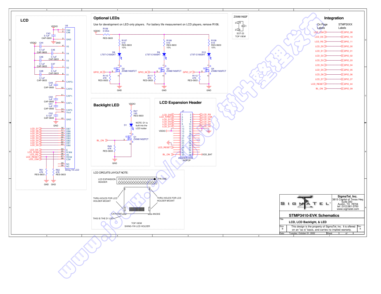
 "MP4播放器STMP3410电路原理图-5")
 "MP4播放器STMP3410电路原理图-6")
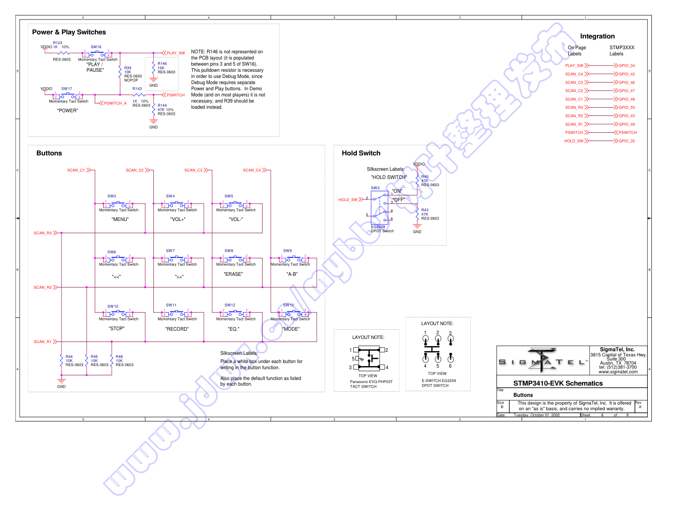
 "MP4播放器STMP3410电路原理图-7")
 "MP4播放器STMP3410电路原理图-8")
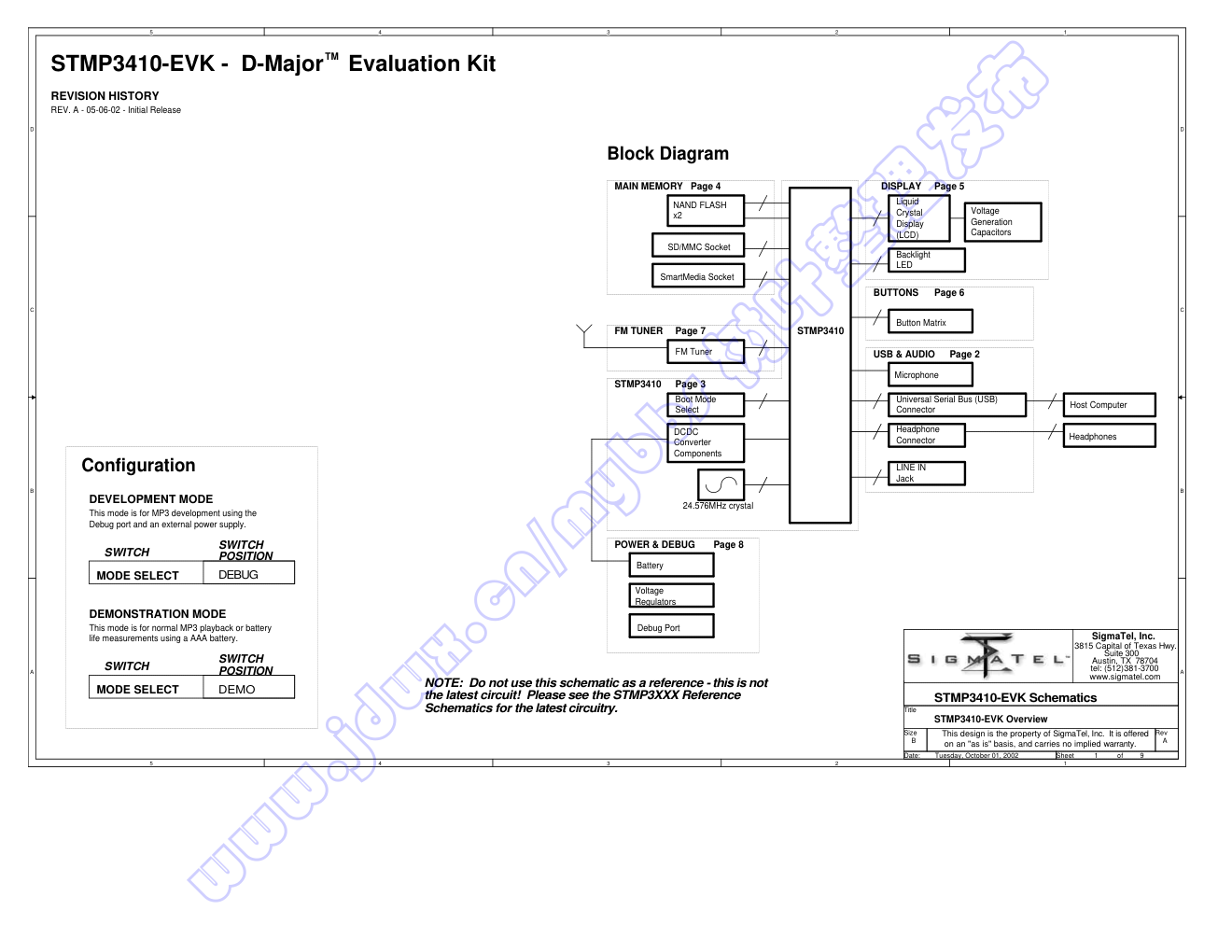
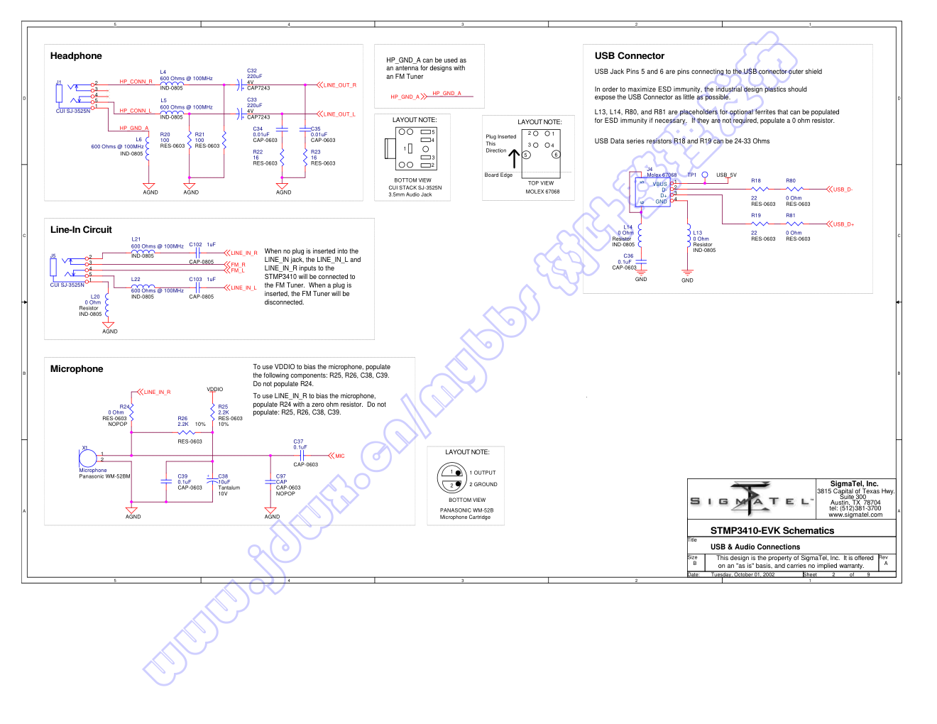
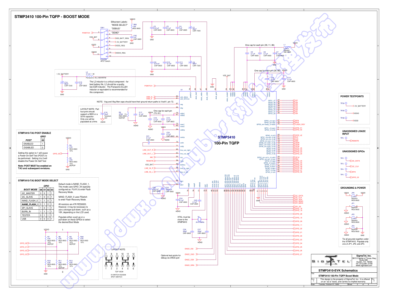
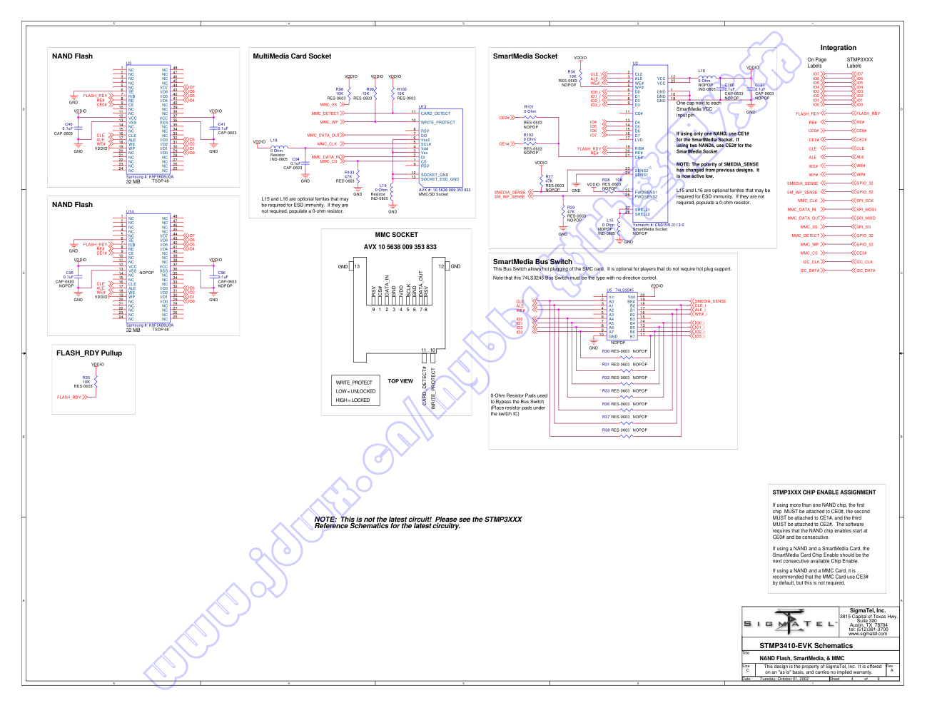
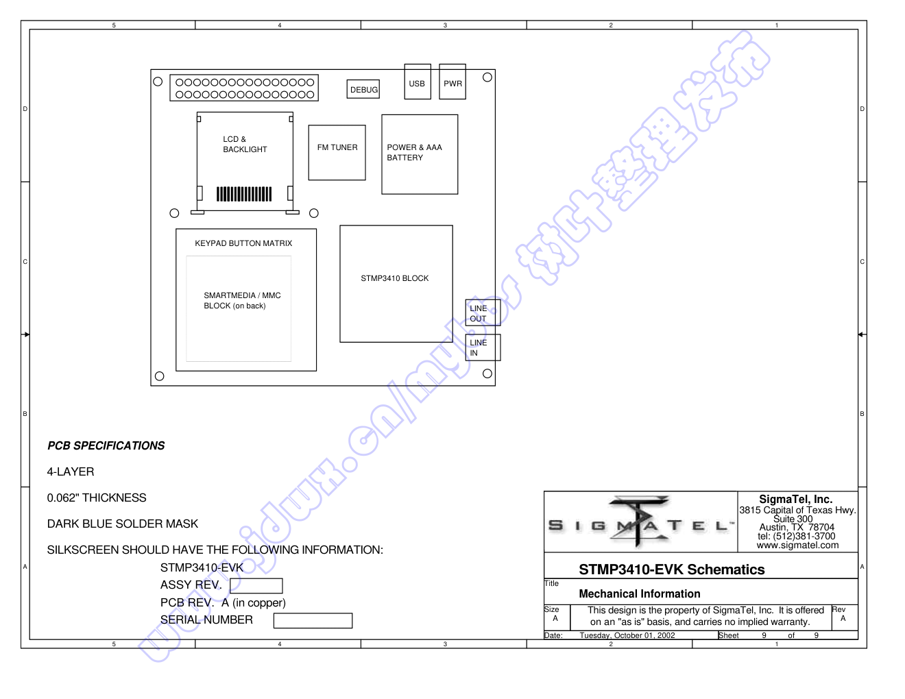
5 5 4 4 3 3 2 2 1 1 D D C C B B A A REVISION HISTORY STMP3410-EVK - D-Major Evaluation Kit REV. A - 05-06-02 - Initial Release SWITCH POSITION DEVELOPMENT MODE DEMO MODE SELECT SWITCH POSITION SWITCH Configuration DEMONSTRATION MODE DEBUG This mode is for MP3 development using the Debug port and an external power supply. MODE SELECT SWITCH This mode is for normal MP3 playback or battery life measurements using a AAA battery. TM Block Diagram SmartMedia Socket Debug Port FM TUNER POWER & DEBUG LINE IN Jack Universal Serial Bus (USB) Connector Voltage Regulators Page 4 Host Computer STMP3410 Voltage Generation Capacitors MAIN MEMORY BUTTONS USB & AUDIO Battery SD/MMC Socket Page 5 STMP3410 Page 7 Button Matrix DISPLAY Page 6 Headphone Connector Boot Mode Select Page 8 NAND FLASH x2 24.576MHz crystal Page 3 FM Tuner Headphones Backlight LED Microphone DCDC Converter Components Liquid Crystal Display (LCD) Page 2 NOTE: Do not use this schematic as a reference - this is not the latest circuit! Please see the STMP3XXX Reference Schematics for the latest circuitry. A STMP3410-EVK Schematics B 1 9 Tuesday, October 01, 2002 STMP3410-EVK Overview Size Rev Date: Sheet of This design is the property of SigmaTel, Inc. It is offered on an "as is" basis, and carries no implied warranty. www.sigmatel.com tel: (512)381-3700 Austin, TX 78704 Suite 300 3815 Capital of Texas Hwy. SigmaTel, Inc. Title www.jdwx.cn/mybbs 树叶整理发布 5 5 4 4 3 3 2 2 1 1 D D C C B B A A Headphone HP_GND_A can be used as an antenna for designs with an FM Tuner To use VDDIO to bias the microphone, populate the following components: R25, R26, C38, C39. Do not populate R24. To use LINE_IN_R to bias the microphone, populate R24 with a zero ohm resistor. Do not populate: R25, R26, C38, C39. Microphone L13, L14, R80, and R81 are placeholders for optional ferrites that can be populated for ESD immunity if necessary. If they are not required, populate a 0 ohm resistor. USB Jack Pins 5 and 6 are pins connecting to the USB connector outer shield USB Connector USB Data series resistors R18 and R19 can be 24-33 Ohms In order to maximize ESD immunity, the industrial design plastics should expose the USB Connector as little as possible. Line-In Circuit When no plug is inserted into the LINE_IN jack, the LINE_IN_L and LINE_IN_R inputs to the STMP3410 will be connected to the FM Tuner. When a plug is inserted, the FM Tuner will be disconnected. BOTTOM VIEW 1 LAYOUT NOTE: 2 4 3 CUI STACK SJ-3525N 3.5mm Audio Jack 5 PANASONIC WM-52B Microphone Cartridge LAYOUT NOTE: BOTTOM VIEW 1 OUTPUT 2 GROUND 1 2 6 LAYOUT NOTE: 2 5 1 4 3 Plug Inserted This Direction TOP VIEW MOLEX 67068 Board Edge A STMP3410-EVK Schematics B 2 9 Tuesday, October 01, 2002 USB & Audio Connections Size Rev Date: Sheet of This design is the property of SigmaTel, Inc. It is offered on an "as is" basis, and carries no implied warranty. www.sigmatel.com tel: (512)381-3700 Austin, TX 78704 Suite 300 3815 Capital of Texas Hwy. SigmaTel, Inc. Title HP_GND_A HP_CONN_L HP_CONN_R HP_GND_A LINE_OUT_R LINE_OUT_L HP_GND_A LINE_IN_R MIC USB_D+ USB_D- LINE_IN_R FM_R FM_L LINE_IN_L VDDIO GND GND USB_5V AGND AGND AGND AGND AGND AGND R24 0 Ohm RES-0603 NOPOP C37 0.1uF CAP-0603 L21 600 Ohms @ 100MHz IND-0805 + C33 220uF CAP7243 4V C39 0.1uF CAP-0603 C97 CAP CAP-0603 NOPOP L14 IND-0805 0 Ohm Resistor R81 0 Ohm RES-0603 L4 600 Ohms @ 100MHz IND-0805 TP1 R21 100 RES-0603 R18 22 RES-0603 L22 600 Ohms @ 100MHz IND-0805 J4 Molex 67068 1 2 3 4 VBUS D- D+ GND 5 6 R23 16 RES-0603 C102 1uF CAP-0805 L5 600 Ohms @ 100MHz IND-0805 C35 0.01uF CAP-0603 J1 CUI SJ-3525N 2 5 1 4 3 R25 2.2K RES-0603 10% L6 600 Ohms @ 100MHz IND-0805 C34 0.01uF CAP-0603 R20 100 RES-0603 R26 2.2K RES-0603 10% X1 Microphone Panasonic WM-52BM 1 2 J5 CUI SJ-3525N 2 5 1 4 3 L20 IND-0805 0 Ohm Resistor C103 1uF CAP-0805 L13 IND-0805 0 Ohm Resistor + C38 10uF Tantalum 10V R19 22 RES-0603 R80 0 Ohm RES-0603 + C32 220uF CAP7243 4V C36 0.1uF CAP-0603 R22 16 RES-0603 www.jdwx.cn/mybbs 树叶整理发布 5 5 4 4 3 3 2 2 1 1 D D C C B B A A STMP3410 100-Pin TQFP - BOOST MODE GROUNDING & POWER UNASSIGNED GPIOs UNASSIGNED LRADC INPUT Tie all grounds together under the STMP3410. Populate only one of JP1, JP2, and JP3. NOTE: Vag and Vbg filter caps should have their ground return paths to VssA1, pin 72. One cap for each pin (29, 96) XTAL must be close to the STMP3410 Silkscreen Labels: "DEMO" Optional test points for debug via ONCE port "MODE SELECT" 100-Pin TQFP "DEBUG" LAYOUT NOTE: Part foot print should support a 0603 or a 3216 capacitor. Only one will be populated at a time. One cap for each pin (39, 11, 86) One cap for each pin (73, 61) The L2 inductor is a critical component - for best battery life, L2 should be a quality, low-ESR inductor. The Panasonic ELL6H inductor or equivalent is recommended for this component. NAND_FLASH_0 uses PSwitch to enter Flash Recovery Mode. I2C_MASTER 1 1 NAND_FLASH_1 GPIO 0 Setting this option to 1 will cause a Power On Self Test (POST) to be performed. Setting it to 0 will disable the Power On Self Test 1 08 0 ENABLED 0 1 1 01 BOOT MODE 1 0 0 1 DISABLED 1 0 1 STMP3410-TA3 POST ENABLE 1 0 0 0 1 0 1 0 BURN_IN 1 1 SPI_SLAVE 1 1 POST GPIO 1 1 1 02 00 1 Default mode is NAND_FLASH_1. This mode uses GPIO_34 (typically configured as PLAY) to enter Flash Recovery Mode. 0 Note: POST MUST be enabled on TA3 and subsequent revisions. I2C_SLAVE Populate either a pull-up or a pull-down on these GPIOs to select the desired Boot Mode 0 All resistors are 47K RES0603. However, it may be necessary to use a stronger pull-down, such as a 10K, depending on the LCD used. 1 TESTER STMP3410-TA3 BOOT MODE SELECT USB NAND_FLASH_0 03 0 1 TOP VIEW LAYOUT NOTE: E-SWITCH EG4208 4PDT SWITCH 6 2 1 3 4 5 12 11 10 7 8 9 POWER TESTPOINTS A STMP3410-EVK Schematics C 3 9 Tuesday, October 01, 2002 STMP3410 100-Pin TQFP Boost Mode Size Rev Date: Sheet of This design is the property of SigmaTel, Inc. It is offered on an "as is" basis, and carries no implied warranty. www.sigmatel.com tel: (512)381-3700 Austin, TX 78704 Suite 300 3815 Capital of Texas Hwy. SigmaTel, Inc. Title REMOTE GPIO_33 I2C_DATA WP# I2C_CLK GPIO_47 IO1 GPIO_52 GPIO_19 GPIO_00 GPIO_04 CLE USB_D+ GPIO_03 GPIO_02 GPIO_48 GPIO_01 CE3# ONCE_DRN IO5 GPIO_46 GPIO_06 IO2 GPIO_05 FLASH_RDY REMOTE LINE_OUT_R CE2# SPI_MOSI USB_D- I2C_CLK GPIO_43 GPIO_35 IO3 GPIO_10 WE# SPI_SCK IO4 ALE ONCE_DSK CE1# LINE_OUT_L ONCE_DSO GPIO_07 LINE_IN_R GPIO_11 WP# RE# SE# IO7 GPIO_09 GPIO_42 GPIO_51 GPIO_34 MIC SPI_MISO I2C_DATA GPIO_18 IO0 GPIO_33 CE0# PSWITCH PSWITCH LINE_IN_L SPI_SS GPIO_44 ONCE_DSI GPIO_50 IO6 GPIO_49 GPIO_32 GPIO_08 GPIO_03 GPIO_01 GPIO_00 GPIO_08 GPIO_02 VDDD GND VDDA AGND AGND VDDIO AGND AGND AGND VDDIO GND VDDA AGND GND VDDIO GND VDDA AGND VDDA GND VDDD GND VDDD_REG GND GND VDD_BATT_REG VDDD VDDIO_REG GND VDD_BAT VDD_BAT GND GND VDDIO VDDIO 1.5V_BATTERY VDD_BAT AGND AGND 1.5V_BATTERY AGND VDDIO VDDD 1.5V_BATTERY L1 IND-0805 0 Ohm Resistor R5 47K RES-0603 10% NOPOP C26 22pF CAP-0603 + C8 68uF CAP-7243 TP24 + C16 10uF Tantalum 10V C18 0.1uF CAP-0603 C13 0.1uF CAP-0603 JP1 RES-0603 NOPOP 1 2 JP2 RES-0603 Resistor 0 Ohm 1 2 R94 47K RES-0603 10% C25 0.1uF CAP-0603 TP3 C11 1uF CAP-0805 C4 1uF CAP-0805 TP25 C19 0.1uF CAP-0603 SW1 EG4208 4PDT Switch 2 1 3 5 4 6 8 11 9 12 7 10 R4 47K RES-0603 10% TP6 C42 1uF CAP-0805 C20 0.1uF CAP-0603 R66 10K RES-0603 C22 0.001uF CAP-0603 R7 47K RES-0603 10% NOPOP C9 0.01uF CAP-0603 R2 470K RES-0603 1% NOPOP TP26 C15 1uF CAP-0805 TP2 C21 0.1uF CAP-0603 C10 0.1uF CAP-0603 + C1 68uF CAP-7243 C3 0.1uF CAP-0603 TP5 C5 0.1uF CAP-0603 C6 0.1uF CAP-0603 R12 47K RES-0603 10% R10 47K RES-0603 10% C7 0.1uF CAP-0603 C12 0.1uF CAP-0603 C23 0.001uF CAP-0603 TP4 C27 22pF CAP-0603 JP3 RES-0603 NOPOP 1 2 U1 STMP3410 64 63 62 65 61 60 55 56 58 57 59 72 70 71 73 75 74 80 81 6 29 28 88 89 90 91 92 93 94 95 82 83 85 84 46 52 51 53 98 99 86 87 100 1 2 3 4 5 25 40 41 42 45 24 43 44 11 10 27 8 9 12 13 17 21 14 15 16 18 19 20 30 31 32 33 34 35 36 37 22 23 26 39 38 54 48 47 50 49 66 67 79 7 68 69 76 77 78 96 97 vddhp vsshp line_out_left line_out_right vdda2 vssa2 mic battery lradc line_in_left line_in_right vssa1 vrefn vrefp vdda1 xtali xtalo usb_dplus usb_dminus testmode vddio1 vssio1 GP7_I2S-data-O2 GP6_I2S-data-O1 GP5_I2S-data-O0 GP4_I2S-sck GP3_I2S-lrclk GP2_I2S-data-I2 GP1_I2S-data-I1 GP0_I2S-data-I0 GP11 GP9 GP10 GP8 once_dsi once_dso once_dsk once_drn GP19_tio1 GP18_tio0 vddd3 vssd3 GP15_SPI-ss GP14_SPI-mosi GP13_SPI-miso GP12_SPI-sck GP16_I2C-scl GP17_I2C-sda GP56_sm-ready_cf-waitn GP46_cf-cdn GP47_cf-ireq GP48_cf-wpn GP49_cf-bvd1 GP45_sm-ce1n_cf-ce0n GP50_cf-resetn GP43_cf-regn vddd2 vssd2 GP55_sm-wpn GP52_cf-iordn GP51_cf-iowrn GP32_cf-a0 GP33_cf-a1 GP37_sm-ce2n_cf-a5 GP41_sm-ale_cf-a9 GP34_cf-a2 GP35_cf-a3 GP36_sm-ce3n_cf-a4 GP38_sm-ce0n_cf-a6 GP39_sm-sen_cf-a7 GP40_sm-cle_cf-a8 GP24_d0 GP25_d1 GP26_d2 GP27_d3 GP28_d4 GP29_d5 GP30_d6 GP31_d7 GP42_cf-a10 GP53_sm-ren_cf-oen GP54_sm-wen vddd1 vssd1 dcdc_mode2 dcdc_vddd dcdc_vddio dcdc_gnd dcdc_batt vbg vag pswitch GP44_cf-ce1n adcl adcr vddpll vddxtal vsspll vddio2 vssio2 R8 47K RES-0603 10% C24 0.1uF CAP-0603 C2 0.01uF CAP-0603 C17 0.1uF CAP-0603 R11 47K RES-0603 10% NOPOP R9 47K RES-0603 10% NOPOP L2 4.7uH 1 W Panasonic: ELL-6SH4R7M + C14 68uF CAP-7243 JP6 RES-0603 0 Ohm Resistor 1 2 Y1 24.576MHz www.jdwx.cn/mybbs 树叶整理发布 5 5 4 4 3 3 2 2 1 1 D D C C B B A A One cap next to each SmartMedia VCC input pin This Bus Switch allows hot plugging of the SMC card. It is optional for players that do not require hot plug support. Note that this 74LS3245 Bus Switch must be the type with no direction control. 0-Ohm Resistor Pads used to Bypass the Bus Switch (Place resistor pads under the switch IC) SmartMedia Bus Switch SmartMedia Socket NOTE: The polarity of SMEDIA_SENSE has changed from previous designs. It is now active low. L15 and L16 are optional ferrites that may be required for ESD immunity. If they are not required, populate a 0-ohm resistor. Integration On Page Labels STMP3XXX Labels MultiMedia Card Socket L15 and L16 are optional ferrites that may be required for ESD immunity. If they are not required, populate a 0-ohm resistor. If using only one NAND, use CE1# for the SmartMedia Socket. If using two NANDs, use CE2# for the SmartMedia Socket FLASH_RDY Pullup 32 MB NAND Flash NAND Flash 32 MB If using a NAND and a SmartMedia Card, the SmartMedia Card Chip Enable should be the next consecutive available Chip Enable. STMP3XXX CHIP ENABLE ASSIGNMENT If using more than one NAND chip, the first chip MUST be attached to CE0#, the second MUST be attached to CE1#, and the third MUST be attached to CE2#. The software requires that the NAND chip enables start at CE0# and be consecutive. If using a NAND and a MMC Card, it is recommended that the MMC Card use CE3# by default, but this is not required. 9 1 2 3 4 5 6 7 8 11 10 CARD_DETECT# WRITE_PROTECT DATA_OUT DATA_IN SCLK CS# VDD GND GND RSV RSV AVX 10 5638 009 353 833 MMC SOCKET TOP VIEW 12 13 GND GND HIGH = LOCKED WRITE_PROTECT LOW = UNLOCKED NOTE: This is not the latest circuit! Please see the STMP3XXX Reference Schematics for the latest circuitry. A STMP3410-EVK Schematics C 4 9 Tuesday, October 01, 2002 NAND Flash, SmartMedia, & MMC Size Rev Date: Sheet of This design is the property of SigmaTel, Inc. It is offered on an "as is" basis, and carries no implied warranty. www.sigmatel.com tel: (512)381-3700 Austin, TX 78704 Suite 300 3815 Capital of Texas Hwy. SigmaTel, Inc. Title IO0_i IO2_i ALE_i WE#_i IO0 IO3 WE# ALE IO3_i IO1_i IO1 CLE_i CLE IO2 FLASH_RDY IO0_i WE#_i IO2_i SM_WP_SENSE RE# IO5 IO3_i IO4 ALE_i CLE_i IO6 IO1_i IO7 SMEDIA_SENSE SMEDIA_SENSE GPIO_32 CE0# CLE IO6 IO5 IO1 SMEDIA_SENSE GPIO_52 ALE RE# ALE IO5 CE2# IO2 FLASH_RDY WP# IO1 RE# IO7 WE# IO2 FLASH_RDY IO6 CE2# CLE WP# IO4 IO4 IO7 IO3 CE0# WE# IO3 IO0 IO0 SM_WP_SENSE SPI_SS GPIO_52 MMC_DATA_IN I2C_DATA MMC_SS I2C_DATA SPI_MISO MMC_DATA_OUT SPI_MOSI I2C_CLK GPIO_32 SPI_SCK I2C_CLK MMC_WP MMC_CS MMC_CLK CE3# MMC_DETECT MMC_DETECT MMC_DATA_IN MMC_WP MMC_DATA_OUT MMC_CLK MMC_SS MMC_CS CE2# CE1# FLASH_RDY CE0# CLE IO5 IO7 IO4 CLE FLASH_RDY IO7 IO1 IO3 ALE IO0 IO5 IO2 WE# IO3 RE# ALE IO1 IO0 IO4 CE1# IO6 IO2 FLASH_RDY IO6 RE# WE# GND VDDIO VDDIO GND GND GND VDDIO GND VDDIO GND GND GND VDDIO VDDIO VDDIO VDDIO GND GND GND GND GND GND VDDIO VDDIO VDDIO VDDIO VDDIO VDDIO VDDIO VDDIO U2 Yamaichi #: CN015R-3113-0 NOPOP SmartMedia Socket 1 2 3 4 5 6 7 8 9 10 11 12 13 14 15 16 17 18 19 20 21 22 23 24 27 28 25 26 GND CLE ALE WE# WP# D0 D1 D2 D3 GND CD# VCC D4 D5 D6 D7 LVD GND R/B# RE# CE# VCC SENS2 SENS1 SHELL1 SHELL2 FWDSENS1 FWDSENS2 C96 0.1uF CAP-0603 NOPOP U3 Samsung #: K9F5608U0A TSOP-48 1 2 3 4 5 6 7 8 9 10 11 12 13 14 15 16 17 18 19 20 21 22 23 24 25 26 27 28 29 30 31 32 33 34 35 36 37 38 39 40 41 42 43 44 45 46 47 48 NC NC NC NC NC SE R/B RE CE NC NC VCC VSS NC NC CLE ALE WE WP NC NC NC NC NC NC NC NC NC I/O0 I/O1 I/O2 I/O3 NC NC NC VSS VCC NC NC NC I/O4 I/O5 I/O6 I/O7 NC NC NC NC R33 RES-0603 NOPOP C100 0.1uF CAP-0603 NOPOP R29 47K RES-0603 NOPOP R101 0 Ohm RES-0603 NOPOP R30 RES-0603 NOPOP U14 Samsung #: K9F5608U0A TSOP-48 NOPOP 1 2 3 4 5 6 7 8 9 10 11 12 13 14 15 16 17 18 19 20 21 22 23 24 25 26 27 28 29 30 31 32 33 34 35 36 37 38 39 40 41 42 43 44 45 46 47 48 NC NC NC NC NC SE R/B RE CE NC NC VCC VSS NC NC CLE ALE WE WP NC NC NC NC NC NC NC NC NC I/O0 I/O1 I/O2 I/O3 NC NC NC VSS VCC NC NC NC I/O4 I/O5 I/O6 I/O7 NC NC NC NC C40 0.1uF CAP-0603 R27 47K RES-0603 NOPOP R34 10K RES-0603 NOPOP L18 IND-0805 0 Ohm Resistor R98 10K RES-0603 R36 RES-0603 NOPOP C41 0.1uF CAP-0603 R103 47K RES-0603 R31 RES-0603 NOPOP R35 10K RES-0603 L15 IND-0805 0 Ohm NOPOP C95 0.1uF CAP-0603 NOPOP R100 10K RES-0603 R32 RES-0603 NOPOP C94 0.1uF CAP-0603 R38 RES-0603 NOPOP U13 AVX #: 10 5638 009 353 833 MMC/SD Socket 1 2 3 4 5 6 7 8 9 10 11 12 13 CS DI Vss Vdd SCLK Vss2 DO RSV RSV WRITE_PROTECT CARD_DETECT SOCKET_GND SOCKET_ESD_GND L19 IND-0805 0 Ohm Resistor R37 RES-0603 NOPOP R99 10K RES-0603 C101 0.1uF CAP-0603 NOPOP U5 74LS3245 NOPOP 1 2 3 4 5 6 7 8 9 10 11 12 13 14 15 16 17 18 19 20 n/c A0 A1 A2 A3 A4 A5 A6 A7 GND B7 B6 B5 B4 B3 B2 B1 B0 BE# Vdd L16 IND-0805 0 Ohm NOPOP R28 10K RES-0603 NOPOP R102 0 Ohm RES-0603 NOPOP www.jdwx.cn/mybbs 树叶整理发布 5 5 4 4 3 3 2 2 1 1 D D C C B B A A Integration On Page Labels LCD STMP3XXX Labels Optional LEDs Use for development on LED-only players. For battery life measurement on LCD players, remove R106. NOTE: D1 is built into the LCD holder Backlight LED CATHODE THRU-HOLES FOR LCD HOLDER MOUNT PIN ONE SHING-YIH LCD HOLDER LCD EXPANSION HEADER THIS IS THE D1 LED TOP VIEW LCD CIRCUITS LAYOUT NOTE: ANODE THRU-HOLES FOR LCD HOLDER MOUNT LCD Expansion Header D SOT-23 S 2 TOP VIEW 1 3 G ZXM61N02F A STMP3410-EVK Schematics B 5 9 Tuesday, October 01, 2002 LCD, LCD Backlight, & LED Size Rev Date: Sheet of This design is the property of SigmaTel, Inc. It is offered on an "as is" basis, and carries no implied warranty. www.sigmatel.com tel: (512)381-3700 Austin, TX 78704 Suite 300 3815 Capital of Texas Hwy. SigmaTel, Inc. Title GPIO_01 GPIO_07 GPIO_02 GPIO_00 GPIO_06 GPIO_09 GPIO_10 GPIO_04 GPIO_03 GPIO_05 GPIO_08 GPIO_11 LCD_RESET LCD_D4 LCD_D0 LCD_D5 LCD_D1 LCD_D6 LCD_D7 LCD_DS LCD_RS LCD_CS# LCD_D2 LCD_D3 BL_ON GPIO_44 LCD_DS LCD_D7 GPIO_07 LCD_D4 LCD_RS LCD_D0 LCD_RESET GPIO_05 GPIO_06 LCD_D1 LCD_D2 LCD_D6 LCD_CS# LCD_D3 LCD_D5 LCD_R/W# BL_ON LCD_CS# LCD_DS LCD_D3 LCD_D4 LCD_D0 LCD_D2 LCD_D5 LCD_D7 LCD_RS LCD_RESET LCD_R/W# BL_ON LCD_D6 LCD_D1 GND VDDIO GND VDDIO GND GND GND GND GND VDDIO GND VDDIO VDDIO VDD_BAT R108 510 RES-0603 10% C50 1uF CAP-0805 U6 Shing Yih LCD 1 2 3 4 5 6 7 8 9 10 11 12 13 14 15 16 17 18 19 20 21 22 23 24 25 26 27 28 29 30 Vdd C86 GND V5 V4 V3 V2 V1 CAP2+ CAP2- CAP1- CAP+ CAP3- Vout GND DB7 DB6 DB5 DB4 DB3 DB2 DB1 DB0 E R/W# A0 RES# CS# NC NC R110 47K RES-0603 R49 47K RES-0603 R112 47K RES-0603 C47 0.1uF CAP-0603 G D S Q2 ZXM61N02FCT 3 1 2 C48 0.1uF CAP-0603 C43 0.1uF CAP-0603 C44 0.1uF CAP-0603 R47 100 RES-0603 R51 47K RES-0603 C46 0.1uF CAP-0603 G D S Q1 ZXM61N02FCT 3 1 2 R111 47K RES-0603 R109 510 RES-0603 10% LTST-C150GKT D10 J7 HEADER 18X2 NOPOP 1 2 3 4 5 6 7 8 9 10 11 12 13 14 15 16 17 18 19 20 21 22 23 24 25 26 27 28 29 30 31 32 33 34 35 36 C52 0.1uF CAP-0603 D1 G D S Q3 ZXM61N02FCT 3 1 2 R107 510 RES-0603 10% R106 0 Ohm RES-0603 G D S Q4 ZXM61N02FCT 3 1 2 C51 1uF CAP-0805 C45 0.1uF CAP-0603 LTST-C150GKT D9 R52 47K RES-0603 C49 1uF CAP-0805 LTST-C150GKT D8 www.jdwx.cn/mybbs 树叶整理发布 5 5 4 4 3 3 2 2 1 1 D D C C B B A A Integration STMP3XXX Labels On Page Labels "EQ." Also place the default function as listed by each button. "ERASE" "A-B" "STOP" "VOL-" Place a white box under each button for writing in the button function. "<<" Silkscreen Labels: "MODE" "RECORD" "MENU" Buttons "VOL+" ">>" 4 3 Panasonic EVQ-PHP03T TACT SWITCH 6 1 3 5 2 LAYOUT NOTE: 1 5 E-SWITCH EG2209 DPDT SWITCH TOP VIEW LAYOUT NOTE: TOP VIEW 2 4 "HOLD SWITCH" "ON" Hold Switch Silkscreen Labels: "OFF" "PLAY / PAUSE" "POWER" Power & Play Switches NOTE: R146 is not represented on the PCB layout (it is populated between pins 3 and 5 of SW16). This pulldown resistor is necessary in order to use Debug Mode, since Debug Mode requires separate Power and Play buttons. In Demo Mode (and on most players) it is not necessary, and R39 should be loaded instead. A STMP3410-EVK Schematics B 6 9 Tuesday, October 01, 2002 Buttons Size Rev Date: Sheet of This design is the property of SigmaTel, Inc. It is offered on an "as is" basis, and carries no implied warranty. www.sigmatel.com tel: (512)381-3700 Austin, TX 78704 Suite 300 3815 Capital of Texas Hwy. SigmaTel, Inc. Title PLAY_SW GPIO_47 SCAN_C1 GPIO_42 GPIO_46 SCAN_R3 SCAN_R1 GPIO_50 PSWITCH PSWITCH SCAN_C2 HOLD_SW SCAN_C3 GPIO_34 SCAN_C4 GPIO_43 GPIO_48 GPIO_35 SCAN_R2 GPIO_49 SCAN_R1 SCAN_C4 SCAN_R2 SCAN_C1 SCAN_R3 SCAN_C2 SCAN_C3 HOLD_SW PSWITCH_A PSWITCH PLAY_SW GND GND VDDIO GND VDDIO GND VDDIO R45 10K RES-0603 R123 1K RES-0603 10% 3 4 1 2 SW12 Momentary Tact Switch SW2 EG2209 DPDT Switch 2 1 3 5 4 6 R143 1K RES-0603 10% R46 10K RES-0603 R146 10K RES-0603 3 4 1 2 SW4 Momentary Tact Switch 3 4 1 2 SW7 Momentary Tact Switch 3 4 1 2 SW13 Momentary Tact Switch R43 47K RES-0603 3 4 1 2 SW10 Momentary Tact Switch R39 10K RES-0603 NOPOP 3 4 1 2 SW5 Momentary Tact Switch 3 4 1 2 SW16 Momentary Tact Switch 3 4 1 2 SW6 Momentary Tact Switch 3 4 1 2 SW8 Momentary Tact Switch R40 47K RES-0603 R44 10K RES-0603 3 4 1 2 SW11 Momentary Tact Switch 3 4 1 2 SW9 Momentary Tact Switch 3 4 1 2 SW17 Momentary Tact Switch 3 4 1 2 SW3 Momentary Tact Switch R144 47K RES-0603 10% www.jdwx.cn/mybbs 树叶整理发布 5 5 4 4 3 3 2 2 1 1 D D C C B B A A Integration On Page Labels Use HP_GND_A as an antenna STMP3XXX Labels LAYOUT NOTE: TOP VIEW PIN 1 J9 J8 PIN 1 A STMP3410-EVK Schematics B 7 9 Tuesday, October 01, 2002 FM Tuner - Philips TEA5767HN Size Rev Date: Sheet of This design is the property of SigmaTel, Inc. It is offered on an "as is" basis, and carries no implied warranty. www.sigmatel.com tel: (512)381-3700 Austin, TX 78704 Suite 300 3815 Capital of Texas Hwy. SigmaTel, Inc. Title FM_CLOCK FM_WE GPIO_18 FM_L FM_L GPIO_19 FM_R FM_R FM_DATA HP_GND_A SE# BUS_EN BUS_EN FM_WE GPIO_51 CE2# FM_R FM_L FM_CLOCK FM_DATA BUS_EN FM_CLOCK FM_L FM_DATA FM_WE FM_R OPT1 OPT2 OPT1 OPT2 MPX MPX HP_GND_A FM_AGND FM_GND FM_AGND FM_AGND FM_GND VDDIO FM_AGND FM_GND VDDIO FM_AGND VDDIO VDDIO FM_AGND FM_AGND FM_AGND FM_AGND FM_AGND VDDIO FM_GND FM_AGND FM_GND GND VDDIO GND FM_AGND C61 33nF CAP-0603 NOPOP JP5 RES-0603 0 Ohm NOPOP 1 2 R125 47K RES-0603 NOPOP L8 CoilCraft#: 0603CS-R10X_BG 180nH @ 150MHz NOPOP R61 47K RES-0603 NOPOP C67 47nF CAP-0603 NOPOP C68 47nF CAP-0603 NOPOP C74 22pF CAP-0603 NOPOP JP4 RES-0603 0 Ohm NOPOP 1 2 C55 22pF CAP-0603 NOPOP C77 2n2F CAP-0603 NOPOP J9 2.0mm HEADER NOPOP 1 2 3 4 5 6 7 8 9 10 11 R127 47K RES-0603 NOPOP R60 33K RES-0603 NOPOP C53 100pF CAP-0603 NOPOP C54 47pF CAP-0603 NOPOP D7 Philips BB202 NOPOP R56 10K RES-0603 NOPOP L12 CoilCraft#: 0603CS-33NX_BG 33nH @ 250MHz NOPOP C57 4n7F CAP-0603 NOPOP TP14 NOPOP C73 1nF CAP-0603 NOPOP C66 47nF CAP-0603 NOPOP Y2 32.768KHz NOPOP C63 33nF CAP-0603 NOPOP TP13 NOPOP C69 100nF CAP-0603 NOPOP C70 100nF CAP-0603 NOPOP R104 0 Ohm RES-0603 NOPOP U9 PHILIPS TEA5767HN NOPOP 36 35 13 34 33 1 32 31 40 14 39 30 38 29 37 2 28 27 15 26 25 3 16 4 17 5 18 6 19 7 20 8 21 9 22 10 23 11 24 12 RFGND RFI1 BUSEN AVCC AGND NC IFGAI NC NC SWP1 LOOPSW NC TCAGC DIFL2 RFI2 CPOP DIFL1 TCIFC SWP2 VREF MPXO VCOT1 XTAL1 VCOT2 XTAL2 VCOVCC PDLF DGND PHLF DVCC NC DATA NC CLOCK LAVO NC RAVO W/R TMUTE BUSM R55 18K RES-0603 NOPOP TP7 NOPOP R128 47K RES-0603 NOPOP C75 22nF CAP-0603 NOPOP C56 100nF CAP-0603 NOPOP L11 CoilCraft#: 0603CS-33NX_BG 33nH @ 250MHz NOPOP C60 33nF CAP-0603 NOPOP R53 100K RES-0603 NOPOP + C114 10uF Tantalum 10V NOPOP C65 33nF CAP-0603 NOPOP C58 22nF CAP-0603 NOPOP C62 100nF CAP-0603 NOPOP R126 47K RES-0603 NOPOP R57 100K RES-0603 NOPOP C76 2n2F CAP-0603 NOPOP D6 Philips BB202 NOPOP J8 2.0mm HEADER NOPOP 1 2 R54 22 RES-0603 10% NOPOP R105 0 Ohm RES-0603 C64 330pF CAP-0603 NOPOP R59 22 RES-0603 10% NOPOP R58 22 RES-0603 10% NOPOP C59 22nF CAP-0603 NOPOP www.jdwx.cn/mybbs 树叶整理发布 5 5 4 4 3 3 2 2 1 1 D D C C B B A A "REG. POWER" Silkscreen Label: PJ-202A Power Jack To use the USB Power circuit, remove R129 and set the MODE SELECT switch to DEMO. The circuit will not function in DEBUG mode. USB Power Circuit REG102GA-A TOP VIEW SOT-223-5 1 2 4 3 6 5 Route GND back to battery negative terminal as either a 30mil trace or as part of a wide digital ground plane AAA BATTERY Silkscreen should show the outline of a battery. Silkscreen text should read: "Warning: do NOT insert battery backwards." DEBUG PORT KEY OPTIONAL HIGH/LOW VOLTAGE SWITCH Attach this jumper to run in Demo mode using the external power supply to provide 1.5V off the regulator into VDD_BAT. Do not use this jumper if a AAA battery is installed or in DEBUG mode. To set V(high) = 3.3V and V(low) = 2.96V, set R113 = 16.2K, R119 = 10.0K, and R13 = 2.0K. To set V(high) = 1.9V and V(low) = 1.58V, set R114 = 5.1K, R121 = 10.0K, and R1 = 10.0K. VDDIO_REG VDDD_REG If not using this option, short R13 and R1, and NOPOP SW14. 2 1 3 TOP VIEW 1 PINOUT Sleeve Shunt Center 3 2 10.0K 5.10K 10.0K 10.0K R(ADJ-GND) Vout = [1 + R(Vout-ADJ)/R(ADJ-GND)] x 1.26V 1.9V 3.3V 16.2K 10.0K R(Vout-ADJ) 3.2V 3.0V Vout 13.7K 15.4K OPTIONAL BATTERY POWER JUMPER 1.5V 10.0K 1.91K C MMBT3904 B A 3 3 TOP VIEW 1 SOT-23 SOT-23 BZX84C2V4 E K 2 TOP VIEW 1 2 TOP VIEW SOT-23 C 1 1 3 2 D SOT-23 G TOP VIEW S 2 E B FMMT591A Si2312DS 3 2 1 TOP VIEW C 2SD2210 SC-62 4 B E 3 C A STMP3410-EVK Schematics B 8 9 Tuesday, October 01, 2002 Power & Debug Size Rev Date: Sheet of This design is the property of SigmaTel, Inc. It is offered on an "as is" basis, and carries no implied warranty. www.sigmatel.com tel: (512)381-3700 Austin, TX 78704 Suite 300 3815 Capital of Texas Hwy. SigmaTel, Inc. Title VDDD_A ONDEZ VDDIO_A VDDD_A VDDIO_A ONCE_DSI ONCE_DRN ONCE_DSO PSWITCH ONCE_DSK PSWITCH_A VDDIO_REG GND GND GND GND GND VDDIO GND 1.5V_BATTERY_S USB_5V USB_5V USB_5V VDD_BAT VDDD_REG VDD_BATT_REG 1.5V_BATTERY_S GND VDDIO GND GND 1.5V_BATTERY VDD_BATT_REG 1.5V_BATTERY_S GND AGND GND GND GND AGND R145 200 10% NOPOP RES-0603 TP8 R135 200 10% NOPOP RES-0603 R65 10K RES-0603 J6 PJ-202A-2.0mm 1 2 R119 10.0K RES-0603 1% R6 2.2K RES-0603 10% R70 10K RES-0603 R1 0 Ohm RES-0603 R114 5.10K RES-0603 1% C108 0.01uF CAP-0603 TP9 R131 150K RES-0603 10% NOPOP R140 10K RES-0603 NOPOP TP10 R133 47K 10% NOPOP RES-0603 R13 0 Ohm RES-0603 Q6 Si2312DS NOPOP + C106 10uF Tantalum 10V LTST-C150GKT D11 D13 BZX84C2V4LT1 2.4V Zener NOPOP U17 REG102GA-A 1 3 5 4 2 6 VIN GND EN ADJ VOUT GND C110 0.01uF CAP-0603 Q7 FMMT591A/SOT NOPOP R122 10.0K RES-0603 1% + C107 10uF Tantalum 10V F1 Littelfuse#: 1812L050PR 500mA R130 100K 10% NOPOP RES-0603 TP11 + C104 10uF Tantalum 10V C112 0.01uF CAP-0603 R121 10.0K RES-0603 1% C111 0.1uF CAP-0603 J3 0.1" HEADER NOPOP 1 2 Q5 MMBT3904 NOPOP C109 0.1uF CAP-0603 R129 0 Ohm RES-0603 Q12 2SD2210 NOPOP R120 510 RES-0603 10% + _ BT1 AAA Battery Holder 1 2 POS NEG Q9 MMBT3904 NOPOP R141 620 RES-0603 10% NOPOP R113 15.4K RES-0603 1% R69 10K RES-0603 U15 REG102GA-A 1 3 5 4 2 6 VIN GND EN ADJ VOUT GND U16 REG102GA-A 1 3 5 4 2 6 VIN GND EN ADJ VOUT GND R132 47K RES-0603 10% NOPOP C113 0.1uF CAP-0603 R3 2.2K RES-0603 10% TP12 SW14 SW DIP-2 CK SDA02H1SKD 1 2 4 3 J2 HEADER 7X2 1 2 3 4 5 6 7 8 9 10 11 12 13 14 R67 10K RES-0603 + C105 10uF Tantalum 10V D12 DL4148 NOPOP MINIMELF R115 1.91K RES-0603 1% R68 10K RES-0603 www.jdwx.cn/mybbs 树叶整理发布 5 5 4 4 3 3 2 2 1 1 D D C C B B A A 4-LAYER FM TUNER PWR USB STMP3410 BLOCK SMARTMEDIA / MMC BLOCK (on back) LCD & BACKLIGHT POWER & AAA BATTERY KEYPAD BUTTON MATRIX LINE OUT LINE IN DEBUG PCB SPECIFICATIONS 0.062" THICKNESS DARK BLUE SOLDER MASK SILKSCREEN SHOULD HAVE THE FOLLOWING INFORMATION: STMP3410-EVK ASSY REV. PCB REV. A (in copper) SERIAL NUMBER A STMP3410-EVK Schematics A 9 9 Tuesday, October 01, 2002 Mechanical Information Size Rev Date: Sheet of This design is the property of SigmaTel, Inc. It is offered on an "as is" basis, and carries no implied warranty. www.sigmatel.com tel: (512)381-3700 Austin, TX 78704 Suite 300 3815 Capital of Texas Hwy. SigmaTel, Inc. Title www.jdwx.cn/mybbs 树叶整理发布
版权声明
1. 本站所有素材,仅限学习交流,仅展示部分内容,如需查看完整内容,请下载原文件。
2. 会员在本站下载的所有素材,只拥有使用权,著作权归原作者所有。
3. 所有素材,未经合法授权,请勿用于商业用途,会员不得以任何形式发布、传播、复制、转售该素材,否则一律封号处理。
4. 如果素材损害你的权益请联系客服QQ:77594475 处理。