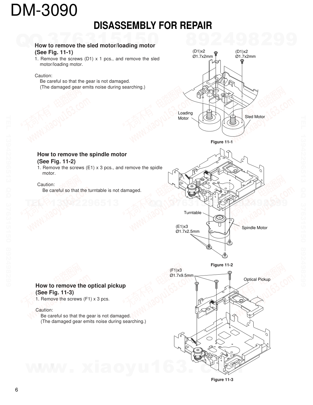
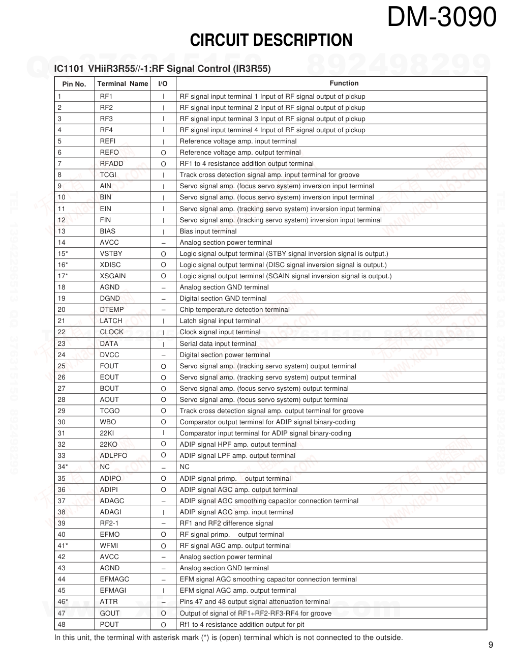
建伍KENWOOD DM-3090 CD播放机维修手册
 "建伍KENWOOD DM-3090 CD播放机维修手册-0")
 "建伍KENWOOD DM-3090 CD播放机维修手册-1")
 "建伍KENWOOD DM-3090 CD播放机维修手册-2")
 "建伍KENWOOD DM-3090 CD播放机维修手册-3")
 "建伍KENWOOD DM-3090 CD播放机维修手册-4")
 "建伍KENWOOD DM-3090 CD播放机维修手册-5")
 "建伍KENWOOD DM-3090 CD播放机维修手册-6")
 "建伍KENWOOD DM-3090 CD播放机维修手册-7")
 "建伍KENWOOD DM-3090 CD播放机维修手册-8")
 "建伍KENWOOD DM-3090 CD播放机维修手册-9")
In compliance with Federal Regulations, following are reproductions of labels on, or inside the product relating to laser product safety, KENWOOD-Corp. certifies this equipment conforms to DHHS Regulation No.21 CFR 1040.10, Chapter 1, Subchapter J. DANGER : Laser radiation when open and interlock defeated. AVOID DIRECT EXPOSURE TO BEAM. *Refer to parts list on page 49. STEREO MINIDISC RECORDER DM-3090 SERVICE MANUAL © 1997-11/B51-5396-00 (K/K) 1812 MULTI CONTROL TIME DISPLAY DISPLAY/CHARAC. TRACK/EDIT ON/STAND BY STEREO MINIDISC RECORDER TIMER/ DELETE ENTER REC REC LEVEL 0 10 PHONES LEVEL MIN MAX PHONES R L R L PLAY OUT REC IN DIGITAL LINE 2 REC IN 1 REC IN PLAY OUT OPT. RESET KENWOOD badge (B43-0302-04) Front glass (B10-2457-08) Front panel (A60-1370-08) Knob (JOG) (K29-6946-08) Knob (REC/HP) (K29-6947-08) AC power cord bushing (J42-0338-08) AC power cord * (E30-) Optical digital output (W02-2643-08) Switch (RESET) (S68-0091-08) Analogue output terminal (E63-1031-08) Optical digital input (W02-2643-08) Knob (POWER) (K27-2261-08) Knob (K27-2262-08) Head phone jack (E11-0345-08) Panel (A29-0898-08) Digital input terminal (E63-1032-08) www. xiaoyu163. com QQ 376315150 9 9 2 8 9 4 2 9 8 TEL 13942296513 9 9 2 8 9 4 2 9 8 0 5 1 5 1 3 6 7 3 Q Q TEL 13942296513 QQ 376315150 892498299 TEL 13942296513 QQ 376315150 892498299 If a problem occurs If this product is subjected to strong external interference (mechanical shock, excessive static electricity, abnormal supply voltage due to lightning, etc.) or if it is operated incorrectly, it may malfunction or the display may not function correctly. If such a problem occurs, do the following: • Unplug the AC power lead from the AC socket. • Wait about 20 - 30 seconds and then plug the AC power lead back into the AC socket. • Press the reset key on the back of the unit. • When the reset key is pressed, all of the settings in memory will be erased. R L R L PLAY OUT REC IN DIGITAL LINE 2 REC IN 1 REC IN PLAY OUT OPT. RESET RESET Beware of condensation When water vapor comes into contact with the surface of cold material, water drops are produced. If condensation occurs, correct operation may not be possible, or the unit may not function correctly. This is not a malfunction, however, and the unit should be dried. (To do this, turn the POWER switch ON and leave the unit as it is for several hours.) Be especially careful in the following conditions: • When the unit is brought from a cold place to a warm place and there is a large temperature difference. • When a heater starts operating. • When the unit is brought from an air-conditioned place to a place of high temperature with high humidity. • When there is a large difference between the internal temperature of the unit and the ambient temperature, or in conditions where condensation occurs easily. 6 1 9 +10 2 3 4 5 7 8 0 Remote control unit (1) (A70-1208-08) Battery cover (A09-0337-08) Audio cord (2) (E30-0505-05) Optical fiber cable (1) (B19-1529-05) Batteries (2) 2 CONTENTS/ACCESSORIES/CAUTIONS CONTENTS/ACCESSORIES/CAUTIONS...................2 CONTROLS .................................................................3 DISASSEMBLY FOR REPAIR.....................................5 BLOCK DIAGRAM .......................................................7 CIRCUIT DESCRIPTION .............................................9 TROUBLE SHOOTING ..............................................16 ADJUSTMENT ...........................................................24 PC BOARD ............................................................... 32 SCHEMATIC DIAGRAM ........................................... 37 EXPLODED VIEW .....................................................47 PARTS LIST...............................................................49 SPECIFICATIONS .......................................Back cover CONTENTS Accessories Cautions www. xiaoyu163. com QQ 376315150 9 9 2 8 9 4 2 9 8 TEL 13942296513 9 9 2 8 9 4 2 9 8 0 5 1 5 1 3 6 7 3 Q Q TEL 13942296513 QQ 376315150 892498299 TEL 13942296513 QQ 376315150 892498299 Names and functions of parts MULTI CONTROL TIME DISPLAY DISPLAY/CHARAC. TRACK/EDIT ON/STAND BY STEREO MINIDISC RECORDER TIMER/ DELETE ENTER REC REC LEVEL 0 10 PHONES LEVEL MIN MAX PHONES 1� � 2� � 3� � 4� � 5� � 6� � 7� � 8� � 9� � 0� � !� � @� � #� � $� � %� � ^� � 1 Eject key: 2 Power switch (ON/STAND BY key) 3 Mini Disc Insertion slot 4 TIME DISPLAY key 5 DISPLAY/CHARAC key 6 TRACK/EDIT key 7 TIMER/DELETE key 8 Jog dial (Next/Previous) 9 ENTER key 0 Headphone jack (HONES) ! Headphone output level control @ Record level control # Record key: $ Play/Pause key: % Stop key: ^ Cue/Review key: / −∞ TOC DISC TOTAL REMAIN RANDOM TIMER REC CLOCK TRACK DATE 0dB OVER 12 4 MONO LP PRGM 1 8 15 2 9 16 3 10 17 4 11 18 5 12 19 6 13 20 7 14 1� �2� � 3� � 4� � 5� � 6� � 7� � 8� � 9� � 0� � !� � @� � #� � $� � %� � ^� � &� � *� � (� � 1 Pause indicator: 2 Record indicator: 3 Play indicator: 4 Monaural Long-Play Mode indicator 5 Programme indicator 6 Repeat indicator: 7 Total Time/Remaining Time indicator 8 Random indicator 9 Timer Playback/Timer Recording indicator 0 Clock indicator ! Music Calendar @ More Tracks indicator # Recording Level indicator $ Recording level too high indicator % Level Meter/Character Information display ^ Date indicator & Track indicator * Disc Name indicator ) TOC Indicator: TOC Front panel Display Display 3 CONTROLS www. xiaoyu163. com QQ 376315150 9 9 2 8 9 4 2 9 8 TEL 13942296513 9 9 2 8 9 4 2 9 8 0 5 1 5 1 3 6 7 3 Q Q TEL 13942296513 QQ 376315150 892498299 TEL 13942296513 QQ 376315150 892498299 Remote control unit POWER DISPLAY TIME DISPLAY 6 1 9 +10 REC MODE PLAY MODE AUTO MARK REC CANCEL SYNCHRO REC REC REC INPUT TRACK EDIT TIMER ENTER PROGRAM CLEAR EJECT 2 3 4 5 7 8 0 SELECT REMOTE CONTROL UNIT RC-M0301 7� � 6� �5� � 4� � 3� � 2� � 1� � 4 Basic operation keys / : Skip down/ Skip up (Cue/Review) key REC : Record key : Stop key : Play/Pause key PLAY MODE : Play mode key 7 Display keys DISPLAY : Display key TIME DISPLAY : Time display key Model: RC-M0301 Infrared ray system PHONES PHONES LEVEL MIN MAX The remote control unit incorporates the basic operation keys as well as a variety of applied operation keys so that it can be used in a wide range of purposes. Use care to store the remote control unit in a safe place so as not to lose it. 1 POWER key 2 EJECT key 3 Numeric keys 6 Recording operation keys REC INPUT: Input select key REC MODE: Record mode key AUTO MARK: Auto mark key REC CANCEL: Record cancel key Plug the stereo headphones (with standard-plug) available in audio stores into the PHONES jack and adjust the listening volume with the PHONES LEVEL control on the front panel. Listening through headphones 5 Applied operation keys ENTET: Entet key TRACK EDIT: Edit key TIMER: Timer key SYNCHRO REC: Synchro recording key PROGRAM: Program key 4 CONTROLS www. xiaoyu163. com QQ 376315150 9 9 2 8 9 4 2 9 8 TEL 13942296513 9 9 2 8 9 4 2 9 8 0 5 1 5 1 3 6 7 3 Q Q TEL 13942296513 QQ 376315150 892498299 TEL 13942296513 QQ 376315150 892498299 REMOVING AND REINSTALLING THE MAIN PARTS MD MECHANISM SECTION Perform steps 1 to 3 of the disassembly method to remove the MD mechanism. How to remove the magnetic head (See Fig. 10-1) 1. Remove the screws (A1) x 1 pc. 10 Caution: Take utmost care so that the magnetic head is not damaged when it is mounted. How to remove the cartridge holder (See Fig. 10-2) 1. Open the roller arm lever in the arrow direction, and lower the clamper lever to the rear side. 2. Apply +5V to the red line side of blue connector of loading motor, push the rack gear in the arrow direction to move the cam plate lever until tick is heard. 3. Remove the screw (B1) x1 pc., and the spring (B2) x1 pc., fitted to the holder arm, and shift the cartridge holder to the left side to remove it. How to remove the mechanism switch PWB (See Fig. 10-3) 1. Remove the screws (C1) x 2 pcs., and remove the mecha- nism switch PWB. Figure 10-1 Figure 10-2 Figure 10-3 MD Mechanism (A1)x1 ø1.7x5mm Magnetic Head Slider Lever Cartridge Holder Clampa Lever Lack Gear Roller Arm Lever Loading Motor Cam Plate Lever (B1) x1 Ø1.7x5mm (B2) x1 (C1)x1 Ø1.7x3mm (C1)x1 Ø1.7x9.5mm MD Mechanism Switch PWB 5 DISASSEMBLY FOR REPAIR www. xiaoyu163. com QQ 376315150 9 9 2 8 9 4 2 9 8 TEL 13942296513 9 9 2 8 9 4 2 9 8 0 5 1 5 1 3 6 7 3 Q Q TEL 13942296513 QQ 376315150 892498299 TEL 13942296513 QQ 376315150 892498299 How to remove the sled motor/loading motor (See Fig. 11-1) 1. Remove the screws (D1) x 1 pcs., and remove the sled motor/loading motor. Caution: Be careful so that the gear is not damaged. (The damaged gear emits noise during searching.) Figure 11-1 Figure 11-2 Figure 11-3 How to remove the spindle motor (See Fig. 11-2) 1. Remove the screws (E1) x 3 pcs., and remove the spidle motor. Caution: Be careful so that the turntable is not damaged. How to remove the optical pickup (See Fig. 11-3) 1. Remove the screws (F1) x 3 pcs. Caution: Be careful so that the gear is not damaged. (The damaged gear emits noise during searching.) Sled Motor Loading Motor (D1)x2 Ø1.7x2mm (D1)x2 Ø1.7x2mm Spindle Motor Turntable (E1)x3 Ø1.7x2.5mm Optical Pickup (F1)x3 Ø1.7x9.5mm 6 DISASSEMBLY FOR REPAIR www. xiaoyu163. com QQ 376315150 9 9 2 8 9 4 2 9 8 TEL 13942296513 9 9 2 8 9 4 2 9 8 0 5 1 5 1 3 6 7 3 Q Q TEL 13942296513 QQ 376315150 892498299 TEL 13942296513 QQ 376315150 892498299 Figure 28BLOCK DIAGRAM (1/2) D6.5/4.75 ~ 5.25V MECHAN1SM 6.5/4.75~5.25V D3.2V SYSCLK DVDD DVDD D3.2V DIGITAL 3.2V D3.2V D4.3V D4.3V D3.2V D4.3V D3.2V BACKUP VOLTAGE REGULATOR POWER IC1402 S29294A E2PROM IC1601 M56758FP 5-CH MOTOR DRIVER BACKUP MD MICRO COMPUTER IC1401 IX0227AW MD SYSTEM MICRO COMPUTER DIGIN(EIAJ) PDOWN DIGOUT(EIAJ) GND GND 1 2 4 3 BCLK MUTE DFS0 DADATA LRCLK ADDATA DFS1 LOAD IN RESET MD-ST DSCK SERCH 1 2 24 23 22 21 20 19 18 17 16 15 14 4 5 6 7 8 9 13 10 11 12 3 D.GND D.GND D.GND D.GND DSTB MDDATA KDATA 4M DRAM ENDEC ATRAC IC1201 LR37648 OSCILLATOR XL1201 (33.8688MHz) SW1956 SW1955 SW1954 SW1953 SW1952 Q1251~Q1254 MD RECORDING HEAD M901 SPINDLE MOTOR M902 SLED MOTOR M903 LOADING SWITCH RECSWITCH PLAYSWITCH LEAD INSWITCH A–BSIGNAL E–FSIGNAL RF1 ~ RF4SIGNAL HEAD DRIVE SIGNAL IC1251 IC1101 IR3R55 RF SIGNAL PROCESSOR LOADING MOTOR HEAD UP/DOWN M M DIRECT SWITCH WRITE PRO M LASER DIODE MONITOR DIODE RF4 RF3 RF2 RF1 LIGHT RECEIVING SECTION ERROR SIGNAL LIGHT RECEIVING SECTION RF F A B E FOCUS TRACKING PICK UP UNIT IC1202 IX2474AF CNP1904 CNP1902 IC1906 AND GATE TC7ST08F IC1907 CLOCK GENERATOR TC92ASF IC1990 INVERTOR 74AC04FS IC1916 AND GATE 74VHC08F 7 BLOCK DIAGRAM www . x ia o y u 1 6 3 . c o m QQ 3 7 6 3 1 5 1 5 0 9 9 2 8 9 4 2 9 8 T E L 1 3 9 4 2 2 9 6 5 1 3 9 9 2 8 9 4 2 9 8 0 5 1 5 1 3 6 7 3 Q Q TEL 13942296513 QQ 376315150 892498299 TEL 13942296513 QQ 376315150 892498299 Figure 29BLOCK DIAGRAM (2/2) LINE IN J101 IC101 NJM4560D OPE AMP +7V +7V -7V -7V REC VOL VR901 SYSCLK AD DATA LRCLK BLCK DA DATA MODE CLK DATA Q601 Q602 IC501 REGULATOR S81233YK J301 DIGITAL -IN (COAXIAL JACK) SO302 DIGITAL IN (OPTICAL JACK) RX302 DIGITAL OUT (OPTICAL JACK) IC301 74HCU04 INVERTER IC302 NAND GATE 74HC10AP DIGITAL IN MD UNIT DIGIN VCC DIGITAL OUT Q503 A-7V POWER CIRCUIT MD+ POWER CIRCUIT 5V SYSTEM POWER CIRCUIT BACK UP 5V DIGITAL 5V MD 5V MD+ S-ID,SYN,RESET,DSTB,DSCK K-DATA,MD DATA FL DISPLAY +B FL901 ~ ~ ~ ~ DIG SEG JOG KEY RX-IN IC901 IX0196AW SYSTEM MICROCOMPUTER MD MUTE SW901 JOG SWITCH KEY IN BLOCK UN970 REMOTE SENSOR FL VP(-31V) A/D +5V BACK UP +5V FL POWER CIRCUIT FL VP(-32V) FL DISPLAY +B RECTIFYING CIRCUIT F551 1A L 250V F552 1A L 250V T551 POWER TRANSFORMER AC 230V 50Hz HEADPHINES J981 H.P.VOL VR981 IC651 NJM4560D OPE AMP Q451 Q452 MUTE J101 LINE OUT 3 4 5 1 7 8 3 5 12 19 16 13 15 24 26 10 2 3 4 5 1 7 2 1 3 8 3 4 5 1 7 8 8 13 2 6 13 10 17 21 21 42 60 89 45 90 92 97 2 3 6 32 10 33 96 91 100 ~ ~ +7V -7V IC201 UDA1340 AD/DA CONVERTER IC601 LINE AMP. NJM4580D Q502 Q506 Q504 A+7V POWER CIRCUIT 3V ~ 8 BLOCK DIAGRAM www . x ia o y u 1 6 3 . c o m QQ 3 7 6 3 1 5 1 5 0 9 9 2 8 9 4 2 9 8 T E L 1 3 9 4 2 2 9 6 5 1 3 9 9 2 8 9 4 2 9 8 0 5 1 5 1 3 6 7 3 Q Q TEL 13942296513 QQ 376315150 892498299 TEL 13942296513 QQ 376315150 892498299 1 RF1 I I I I I I I I I I I I I I O O O O O O O O O I O O O O – – – – – – – – – – I – I O O O O – O O RF signal input terminal 1 Input of RF signal output of pickup 2 RF2 RF signal input terminal 2 Input of RF signal output of pickup 3 RF3 RF signal input terminal 3 Input of RF signal output of pickup 4 RF4 RF signal input terminal 4 Input of RF signal output of pickup 5 REFI Reference voltage amp. input terminal 6 REFO Reference voltage amp. output terminal 7 RFADD RF1 to 4 resistance addition output terminal 8 TCGI Track cross detection signal amp. input terminal for groove 9 AIN Servo signal amp. (focus servo system) inversion input terminal 10 BIN Servo signal amp. (focus servo system) inversion input terminal 11 EIN Servo signal amp. (tracking servo system) inversion input terminal 12 FIN Servo signal amp. (tracking servo system) inversion input terminal 13 BIAS Bias input terminal 14 AVCC Analog section power terminal 15* VSTBY Logic signal output terminal (STBY signal inversion signal is output.) 16* XDISC Logic signal output terminal (DISC signal inversion signal is output.) 17* XSGAIN Logic signal output terminal (SGAIN signal inversion signal is output.) 18 AGND Analog section GND terminal 19 DGND Digital section GND terminal 20 DTEMP Chip temperature detection terminal 21 LATCH Latch signal input terminal 22 CLOCK Clock signal input terminal 23 DATA Serial data input terminal 24 DVCC Digital section power terminal 25 FOUT Servo signal amp. (tracking servo system) output terminal 26 EOUT Servo signal amp. (tracking servo system) output terminal 27 BOUT Servo signal amp. (focus servo system) output terminal 28 AOUT Servo signal amp. (focus servo system) output terminal 29 TCGO Track cross detection signal amp. output terminal for groove 30 WBO Comparator output terminal for ADIP signal binary-coding 31 22KI Comparator input terminal for ADIP signal binary-coding 32 22KO ADIP signal HPF amp. output terminal 33 ADLPFO ADIP signal LPF amp. output terminal 34* NC NC 35 ADIPO ADIP signal primp. output terminal 36 ADIPI ADIP signal AGC amp. output terminal 37 ADAGC ADIP signal AGC smoothing capacitor connection terminal 38 ADAGI ADIP signal AGC amp. input terminal 39 RF2-1 RF1 and RF2 difference signal 40 EFMO RF signal primp. output terminal 41* WFMI RF signal AGC amp. output terminal 42 AVCC Analog section power terminal 43 AGND Analog section GND terminal 44 EFMAGC EFM signal AGC smoothing capacitor connection terminal 45 EFMAGI EFM signal AGC amp. output terminal 46* ATTR Pins 47 and 48 output signal attenuation terminal 47 GOUT Output of signal of RF1+RF2-RF3-RF4 for groove 48 POUT Rf1 to 4 resistance addition output for pit IC1101 VHiiR3R55//-1:RF Signal Control (IR3R55) Pin No. Terminal Name I/O Function In this unit, the terminal with asterisk mark (*) is (open) terminal which is not connected to the outside. CIRCUIT DESCRIPTION 9 www. xiaoyu163. com QQ 376315150 9 9 2 8 9 4 2 9 8 TEL 13942296513 9 9 2 8 9 4 2 9 8 0 5 1 5 1 3 6 7 3 Q Q TEL 13942296513 QQ 376315150 892498299 TEL 13942296513 QQ 376315150 892498299 1* EFMMON Output EFM monitor output 2 AVCC — Analog power 3 EFMI Input EFM signal input from RF amp. 4 AGND — Analog GND 5 AIN Input Focus error signal A 6 EIN Input Tracking error signal E 7 TCG Input Track cross signal 8 BIN Input Focus error signal B 9 FIN Input Tracking error signal F 10* VBAT Input Power voltage detection signal for constant voltage servo 11 WBI Input ADIP wobble signal 12 VDD1 — Digital power 13 DGND — Digital GND 14,15 TEST0,TEST1 Input Input for test. Connection to GND in case of normal use 16 TEST2 Input Input for test. Endecode/servo mode and ATRAC mode selection 17 X176KO Output Clock output. f=176.4 kHz (4fs) 18 FODRF Output Focus servo forward output. PWM 19 FODRR Output Focus servo reverse output. PWM 20 TRDRF Output Tracking servo forward output. PWM 21 LATCH Output Tracking servo reverse output. PWM 22 CLOCK Output Slide servo forward output. PWM 23 DATA Output Slide servo reverse output. PWM 24 DVCC Output Spindle servo forward output or spindle servo output. PWM 25 FOUT Output Spindle servo reverse output or spindle rotation (forward/reverse)selection 26 EOUT Output Address output to external D-RAM. ADR3 27 BOUT Output Address output to external D-RAM. ADR2 28 AOUT Output Address output to external D-RAM. ADR1 29 TCGO Output Address output to external D-RAM. ADR0 (LSB) 30* WBO Output Address output to external D-RAM. ADR10 (MSB) 31 22KI — Power supply for DRAM interface 32 22KO Output Address output to external D-RAM. ADR4 33 ADLPFO Output Address output to external D-RAM. ADR5 34 NC Output Address output to external D-RAM. ADR6 35 ADIPO Output Address output to external D-RAM. ADR7 36 ADIPI Output Address output to external D-RAM. ADR8 37 ADAGC Output Data output enable signal output to external D-RAM 38 ADAGI — Digital GND 39 RF2-1 Output Column address strobe signal output to external D-RAM 40 EFMO In/Output Data input/output from and to external D-RAM. D2 41 WFMI In/Output Data input/output from and to external D-RAM. D3 (MSB) 42 AVCC Output Data input/output from and to external D-RAM. ADR9 43 AGND Output Low address strobe signal output to external D-RAM 44 EFMAGC Output Data write enable signal output to external D-RAM 45 EFMAGI In/Output Data input/output from and to external D-RAM. D1 46 ATTR In/Output Data input/output from and to external D-RAM. D0 (LSB) 47* GOUT Output Track cross signal 48* POUT Output ADIP CRC error flag monitor output 49* PLCK Output EFM PLL clock output in playback mode 50 EFM0 Output EFM signal output in record mode. C1F (C1 error flag) monitor output in playback mode 51* X700KO Output Clock output. f = 705.6 kHz. Clock output is not performed when RSTX = 0. 52* EXPORT0 Output Microcomputer extension output port 0 53* EXPORT1 Output Microcomputer extension output port 1 IC1201 VHiLR37648/-1:ENDEC/ATRAC (LR37648) Pin No. Terminal Name Function In this unit, the terminal with asterisk mark (*) is (open) terminal which is not connected to the outside. Input/Output CIRCUIT DESCRIPTION 10 www. xiaoyu163. com QQ 376315150 9 9 2 8 9 4 2 9 8 TEL 13942296513 9 9 2 8 9 4 2 9 8 0 5 1 5 1 3 6 7 3 Q Q TEL 13942296513 QQ 376315150 892498299 TEL 13942296513 QQ 376315150 892498299 54 TESO1 Output PLLLR. Microcomputer extension output port 2 in case of selection 55 TESO3 In/Output PLLOSC. Microcomputer extension output port 3 in case of selection 56 TEST4 In/Output EXTCLK. Microcomputer extension output port 4 in case of selection 57 CDDATA In/Output High speed dubbing CD data input. Microcomputer extension output port 5 in case of selection 58 CDLRCK In/Output High speed dubbing CD LR data input. Microcomputer extension output port 6 in case of selection 59 CDBCLK In/Output High speed dubbing CD bit data input. Microcomputer extension output port 7 in case of selection 60 VXI Input Vari-pitch PLL clock input 61 VPO Output Vari-pitch PLL phase error output 62 VDD1 — Digital power 63 DGND — Digital GND 64 XI Input Oscillation circuit input. 33.8688 MHz 65 XO Output Oscillation circuit input. 33.8688 MHz 66 DIN Input Digital input signal 67 DOUT Output Digital output signal 68 VDD3 — Power for internal PLL 69 DGND — Digital GND 70 LRCK Output Music data Lch/Rch selection output 71 BLCK Output Music data shift clock 72 DFCK Output AD/DA converter digital filter clock. 256 Fs 73 ADDATA Input Audio data input 74 DADATA Output Audio data output 75* FEMON Output Focus error signal monitor output 76* TOTMON Output Total signal monitor output 77* TEMON Output Tracking error signal monitor output 78* SBCK Input DIN subcode read clock. EIAJ CP-309 Format 79* SBO Output DIN subcode serial data. EIAJ CP-309 Format 80* SBSY Output DIN subcode block sync signal. EIAJ CP-309 Format 81 SFSY Output DIN subcode frame sync signal. EIAJ CP-309 Format 82 FOK Output Focus OK detection signal. "0" : Focus OK 83 SENSE Output Servo status detection signal. "1": Auto-move, auto-jump, auto-focus retraction 84 COUT Output Track cross signal output 85 MCCK Output Microcomputer clock output. Clock output is performed also when RSTX = 0. 86 DINTX Output System controller interface interruption request output terminal 87 VDD1 — Digital power 88 DGND — Digital GND 89 RSTX Input Chip reset input. "L": Reset 90 SYD0 In/Output System controller interface data bus terminal (LSB) 91~96 SYD1~SYD6 In/Output System controller interface data bus terminal 97 SYD7 In/Output System controller interface data bus terminal (MSB) 98 SYWRX Input System controller interface register writing pulse input 99 SYRDX Input System controller register read pulse input 100 SYRS Input System controller interface register selection input Pin No. Terminal Name Function In this unit, the terminal with asterisk mark (*) is (open) terminal which is not connected to the outside. Input/Output 11 CIRCUIT DESCRIPTION www. xiaoyu163. com QQ 376315150 9 9 2 8 9 4 2 9 8 TEL 13942296513 9 9 2 8 9 4 2 9 8 0 5 1 5 1 3 6 7 3 Q Q TEL 13942296513 QQ 376315150 892498299 TEL 13942296513 QQ 376315150 892498299 1* P96/ANEX1 Output Not used 2* P95/ANEX0 Output Not used 3 P94/DA1 Output LDVAR (laser power adjustment output) 4* P93/DA0 Output ADJS (for automatic adjustment step check) 5* P92/TB2IN Output Not used 6 P91/TB1IN Input LD SW CK input (interruption input only in single state) 7 P90/TB0IN Input ERR input (monitor PLL UNLOCK) 8 BYTE Input GND 9 CNVss Input GND 10* P87/XCIN Output ST-ID Output 11* P86/XOUT Output MD search output 12 RESET Input RESETInput 13* XOUT — Extal clock output 14 Vss — GND 15 XIN Input EXTAL (8.4672 MHz) 16 Vcc — + 3.15V 17 P85/NMI Input Connect +B 18 P84/INT2 Input DINT (interruption input from MD LSI) 19 P83/INT1 Input DSENSE (servo sense input from MD LSI) 20 P82/INT0 Input ST-ID Input (MD-ON) 21 P81/TA4IN Input CD search input (syncro REC suspension input from MD LSI) 22 P80/TA4OUT Output MD RSW Output 23* P77/TA3IN Input FSW1 (SW power frequency selection) 24 P76/TA3OUT Output Vari-pitch correspondence given (H)/not given (L) 25 P75/TA2IN Input P-DOWN (power failure detection) 26 P74/TA2OUT Output HDON (magnetic head current ON/OFF output) 27 P73/TA1IN Output LD+ (loading motor + control output) 28 P72/TA1OUT Output LD- (loading motor + control output) 29 P71/TA0IN Input CIN (track count signal input) 30 P70/TA0OUT Input INN SW (inner SW detection input) 31 P67/TXD1 Output R-DATA 32 P66/RXD1 Output R-LATCH 33 P65/CLK1 Output R-CLK 34 P64/CTS1/RTS1/ Output DSTB (system controller communication enable and communication beingexecuted) CTS0/CLKS1 35 P63/TXD0 Output MD DATA (MD Data Output) 36 P62/RXD0 Input K DATA (system controller data input) 37 P61/CLK0 Input DSCK (system controller communication clock input) 38 P60/CTS0/RTS0 Input 4M/16M DRAM selection input 39 P57/RDY/CLKOUT Output R/P output (REC/PLAY selection) 40 P56/ALE Input FOK (focus servo status monitor input) 41* WFMI Input/Output Not used 42 AVCC Output S2 Ouput 43 AGND Output S1 Output 44 EFMAGC Output SYRS (MD-LSI register selection signal output) 45 EFMAGI Output SYRD (MD-LSI read signal output) 46 ATTR Output SYWR (MD-LSI right signal output) 47 GOUT In/Output SYS D7 (data bus 7) 48 POUT In/Output SYS D6 (data bus 6) 49 PLCK In/Output SYS D5 (data bus 5) 50 EFM0 In/Output SYS D4 (data bus 4) 51 X700KO In/Output SYS D3 (data bus 3) IC1401 RX-iX0227AWZZ:MD System Microcomputer (IX0227AW) Pin No. Terminal Name Function In this unit, the terminal with asterisk mark (*) is (open) terminal which is not connected to the outside. Input/Output 12 CIRCUIT DESCRIPTION www. xiaoyu163. com QQ 376315150 9 9 2 8 9 4 2 9 8 TEL 13942296513 9 9 2 8 9 4 2 9 8 0 5 1 5 1 3 6 7 3 Q Q TEL 13942296513 QQ 376315150 892498299 TEL 13942296513 QQ 376315150 892498299 52 P42/A18 In/Output SYS D2 (data bus 2) 53 P41/A17 In/Output SYS D1 (data bus 1) 54 P40/A16 In/Output SYS D0 (data bus 0) 55* P37/A15 Output Not used 56* P36/A14 Output Not used 57* P35/A13 Output Not used 58 P34/A12 Output EEPRO (EEPROM protection cancel) 59 P33/A11 Output EPCS (EEPROM chip selector output) 60 P32/A10 In/Output EEPD (EEPROM sirial data output) 61 P31A9 Output EEPK (EEPROM sirial colck output) 62 Vcc Input + 3.15V 63* P30/A8 Output Not used 64 Vss — GND 65* P27/A7 Output L3 DATA (soft serial communication, 2 modes provided, LSB fast) 66* P26/A6 Output L3 MODE (soft serial communication, 2 modes provided, LSB fast) 67* P25/A5 Output L3 CLK (soft serial communication, 2 modes provided, LSB fast) 68* P24/A4 Output Not used 69* P23/A3 Output Not used 70 P22/A2 Output PCNT0 output 71* P21/A1 Output Not used 72 P20/A0 Output LDON output (H: ON) 73 P17/D15 Output ANLPTR output 74* P16/D14 Output ADPON output (for CK) 75* P15/D13 Output DAPON output (for CK) 76 P14/D12 Output DFS0 output 77 P13/D11 Output DFS1 output 78* P12/D10 Output DIG EX output (for CK) 79* P11/D9 Output DIG CD output (for CK) 80 P10/D8 Output XRST (system reset output) 81* P07/D7 Output AD MUTE output (for CK) 82* P06/D6 Output EMPHA output (for CK) 83* P05/D5 Output DA MUTE output (for CK) 84 P04/D4 Output MUTE output 85* P03/D3 Output DOUTM output (for CK) 86 P02/D2 Input TEST2 (special mode selection 2) 87 P01/D1 Input TEST1 (special mode selection 1) 88 P00/D0 Input TEST0 (special mode selection 0) 89 P107/AN7/KI3 Input AVCK3 (special mode monitor input) 90 P106/AN6/KI2 Input AVCK2 (AD/DA section 3.1V monitor input) 91 P105/AN5/KI1 Input AVCK1 (DOUT section 5V monitor input) 92 P104/AN4/KI0 Input DTEMP (temperature detection input) 93 P103/AN3 Input MINF (disc type/REC input) 94 P102/AN2 Input TEST K1 (test key input 1) 95 P101/AN1 Input TEST K2 (test key input 2) 96 AVss — GND 97 P100/AN0 Input HINF (mechanism position/HEAD position) 98 VREF — + 3.15V 99 AVcc — + 3.15V 100 P97/ADTRG Input Connect +B Pin No. Terminal Name Function In this unit, the terminal with asterisk mark (*) is (open) terminal which is not connected to the outside. Input/Output CIRCUIT DESCRIPTION 13 www. xiaoyu163. com QQ 376315150 9 9 2 8 9 4 2 9 8 TEL 13942296513 9 9 2 8 9 4 2 9 8 0 5 1 5 1 3 6 7 3 Q Q TEL 13942296513 QQ 376315150 892498299 TEL 13942296513 QQ 376315150 892498299 CIRCUIT DESCRIPTION 14 IC901 RH-iX0196AFZZ: System Control Microcomputer (iX0196AW) Pin No. Function Port Name Input/Output Terminal Name In this unit, the terminal with asterisk mark (*) is (open) terminal which is not connected to the outside. 1* P77/AN7 KEY1 Output Not used 2 P76/AN6 KEY2 Input Key entry 3 P75/AN5 KEY3 Input Key entry 4* P74/AN4 — Output Not used 5 P73/AN3 INI Input Initial setting entry 6 P72/AN2 JOG_AD Input Jog dial entry 7*,8* P71/AN1,P70/AN0 — Output Not used 9* PB3 — Output Not used 10 PB2/DA DIG SEL1 Output Digital signal selector selection signal 11* P57/SRDY3/AN15 DIG SEL2 Output Not used 12* P56/SCLK3/AN14 — Output Not used 13* P55/SOUT3/AN13 — Output Not used 14 P54/SIN3/AN12 DAC_MODE Output Externally provided DAC/ADC serial interface mode signal 15 P52/SRDY2/AN11 DAC_CLK/EX Output Externally provided DAC/ADC serial interface clock signal 16 P52/SCLK2/AN10 DAC_DATA/EX Output Externally provided DAC/ADC serial interface clock signal 17* P51/SOUT2/AN9 — Output Not used 18 P50/SIN2/AN8 DFS0/DFS1 Input EMPHASIS information from MD 19 P67/SRDY1/CS/ DSTRB Input MD serial interface strobe signal SCLK12 20 P66/SCLK1 DSCK Output MD serial interface clock signal 21 P65/SOUT1 K-DATA Output MD serial interface transmission signal 22 P64/SIN1 MD-DATA Input MD serial interface reception signal 23 P63/CNTR1 MD-LO/EJ Output MD loading power voltage selection signal 24* P62/CNTR0 — Output Not used 25* P61/PWM — Output Not used 26* P60 — Output Not used 27* P47/T3OUT — Output Not used 28* P46/T1OUT — Output Not used 29 P45/INT1/2CR P IN Input Power failure detection 30* P44/INT4 P.CNT Output Power control 31 P41 P-OUT Output MD power failure detection signal 32 P42/INT2 RX-IN Input Remote control loght reception signal 33 P41 P-MUTE Output Audio mute control signal 34 P40/INT0 — Input GND 35 RESET RESET Input RESET signal entry 36 PB1/Xcin Xcin Input Sub clock IN connection (32.7k) 37 PB0/Xcout Xcout Output Sub clock OUT connection (32.7k) 38 Xin Xin Input Main clock IN connection (8M) 39 Xout Xout Output Main clock OUT connection (8M) 40 VSS VSS Input GND 41 P27 SERCH Output CD to MD search monitor signal 42 P26 LOAD Input MD loading detection 43 P25 S-ID Output CD to MD start ID signal 44 P24 MD RESET Output RESET signal to MD www. xiaoyu163. com QQ 376315150 9 9 2 8 9 4 2 9 8 TEL 13942296513 9 9 2 8 9 4 2 9 8 0 5 1 5 1 3 6 7 3 Q Q TEL 13942296513 QQ 376315150 892498299 TEL 13942296513 QQ 376315150 892498299 CIRCUIT DESCRIPTION 15 Pin No. Function Port Name Input/Output Terminal Name 72-80 P97/SEG23- S0-S8 Output Segment for FL drive P90/SEG16 81-88 P87/SEG15- S9-S16 Output Segment for FL drive P80/SEG8 89,90 PA7/SEG7, S17,S18 Output Segment for FL drive PA6/SEG6 91 VCC VCC Input +5V 92-97 PA5/SEG5- S19-S24 Output Segment for FL drive PA0/SEG0 98 VEE VEE Input -30V 99 AVSS AVSS Input GND 100 VREF VREF Input +5V 45-54 P23/DIG19- UDIG0-UDIG9 Output Digit for FL drive P12/DIG10 55,56 P11/SEG41/DIG9, UDIG10,UDIG11 Output Digit for FL drive P10/SEG40/DIG8 57-60 P07/SEG39/DIG7- UDIG12-UDIG15 Output Digit for FL drive P04/SEG36/DIG4 61-64 P05/SEG35/DIG3- S35-S32 Output Segment for FL drive P00/SEG33/DIG0 65-72 P37/SEG31- S31-S25 Output Segment for FL drive P30/SEG25 www. xiaoyu163. com QQ 376315150 9 9 2 8 9 4 2 9 8 TEL 13942296513 9 9 2 8 9 4 2 9 8 0 5 1 5 1 3 6 7 3 Q Q TEL 13942296513 QQ 376315150 892498299 TEL 13942296513 QQ 376315150 892498299 TROUBLE SHOOTING 16 BLANK MD Can't COPY Can't EDIT Can't REC DEFECT Din UNLOCK DISC ERR DISC FULL FOCUS ERROR MECHA ERR** NAME FULL NO DISC NOT AUDIO PLAYBACK MD PROTECTED TEMP OVER TOC ERR** TOC FULL** TOC W ERROR U TOC ERR** U TOC W ERR ? DISC 0-00:00 **Number or symbol Error messages Meaning Remedy Nothing is recorded. • • No copy can be made because of the SCMS copyright system. • A track cannot be edited. • Recording cannot be pertormed correctly due to vibration. • Since this MD has scratches on it, the recording operation was skipped. • Poor connection of the digital cable. • The disc damaged. • The TOC information is not recorded on the disk or the date contains. • The MD is out of recording space. • A MD has not been loaded. • The disc data cannot be read. • There is a mechanical problem and the disc is working properly. • The number of characters for the MD name or track name exceeds 40. • MD has not been loaded. • MD data cannot be read. • The data recorded on this disc is not audio data. • You tried to record on a playback-only disc. • The MD is write protected. • The temperature is too high. • The MD is excessively damages • There is no space left for recording character infomation (track names, disc names, etc.) • Trouble has occurred. • The TOC infomation on this disc does not meet the MD specifications or it cannot be read. • The TOC infomation could not be created properly due to a mechanical shock or to scratches on the disc. • The MD contains an error. • Music is not being recorded. • Replace the MD wiht a recoded disc. • Record using the analogue cable. • Change the stop position of the track and then try editing it. • Stop vibration and try again. • Replace the disc with another recordable disc. • Connect the digital cable securely. • Reload the disc or replace it. • Replace the disc with another recordable disc. • Reload the MD. • Reset the microprocessor referring to "If a problem occurs". • Shorten the MD or track name. • Load a MD. • Reload the MD. • Select another track. • Replace the MD. • Raplace it with a recordable MiniDisc. • Move the write protection tab back to its original position. • Turn off the power, and wait for a whilst. • Replace the disc with another disc. • Replace the MD with another recordable disc. • Contact a KENWOOD Authorized Sevicing Dealer or KENWOOD Authorized Sevice station. • Replace it with another MD. • Erase all the data, and try recording. • Turn off the power, and try to write the TOC- information again. (Remove any source of shock or vibration whilst writing.) • Replace the disc with another disc. • Replace the disc with a recorded disc. When an error message is displayed, proceed as follows: www. xiaoyu163. com QQ 376315150 9 9 2 8 9 4 2 9 8 TEL 13942296513 9 9 2 8 9 4 2 9 8 0 5 1 5 1 3 6 7 3 Q Q TEL 13942296513 QQ 376315150 892498299 TEL 13942296513 QQ 376315150 892498299 • Defect occurred successively 10 times during REC-PLAY. • As a result of occurrence of defect during REC-PLAY the recordable cluster became zero. • Adress is unreadable. REC state connot be set for 20 seconds although retry is repeated. • The following judgement is made according to the channel status of digital signal which was input from D-IN during REC- PAUSE or REC-PLAY. (1) Other than audio signal (2) Other than signals of home-use appliances (3) Copy NG due to inversion of copy bit in CD. • The digital signal which was input from D-IN during REC- PAUSE, REC-PLAY or CD FUNC playback caused the following. (1) PLL of digital IN was unlocked. (2) Locking occurred in condition other than FS = 44.1 kHz • There were no areas to record music or character infomation.(music name, disc name, etc.) during REC-PLAY. • When an attempt to start is made, recordable area does not remain. • ETNO > LTNO • FTNO ≠ 0 or 1 • UTOC recorded on disc could not be read. • Start address > End address • Any data of UTOC 0 to 4 looped. • Nonaudio data was recorded in the track mode of currently selected TNO. • Data "MINI" of system ID which has been written in TOC with ASCII code is not correct. • The disc type written i TOC does not correcpond to pre/ mastered MD, recording MD and hybrid MD. • When an attempt to set REC-PAUSE was made, there were no recordable areas. • An attempt to set REC-PAUSE or to start editing was made on the playback-only disc. • An attempt to record or edit was made on the record/playback disc with its careless rease preventing tab being in rease preventing state. • An attempt was made t oedit the track which was write- protected by information written in UTOC. • Specific editing conditions were not satisfied. • Owing to occurrence of some trouble internal temperature of set (MD unit) rose excessively. • Read data was not correct or data could not be read correctly. • Trouble occurred during recording if music data, resulting in EXPLANATION OF ERROR DISPLAY Error display Errors Corrective action Can't REC Can't COPY Din UNLOCK TOC FULL UTOC ERR R UTOC ERR A UTOC ERR L0~4 NOT AUDIO ? DISC DISC FULL PLAYBACK MD PROTECTED Can't EDIT TEMP OVER DISC ERR RD PA • Check that the disc is free from flaw, dust and fingerprint. Check whether there is any black spot. Check for disc disalignment and run-out. • Check whether CD is copy-inhibited one. (An exabple: CD-R) • Check whether there is any abnormality in the D-IN signal line. • Replace the disc with a recording/ playback disc in which an area to register UTOC remains. • UTOC data is not normal. Replace the disc with other disc. • UTOC data is not normal. Replace the disc with other disc. • UTOC data is not normal. Replace the disc with other disc. • Select other TNO or replace the disc with other disc. • The loaded disc is not applicable. Replace the disc, and check. • Replace the disc with other recording disc in which recording area remains. • The loaded disc is a Playback-only disc. Replace the disc with a recording disc. • Return the careless erase preventing tab to its initial position, and redo. • The track on which an attempt to edit was made is a write-protected track. Redo on another track. • The applied operation procedure is not proper. Redo, applying the ocrrect procedure. • Check by troubleshooting. • Check whether the ambient temperature is too high. • Data of TOC or UTOC is not normal or disc las flaw. Replace the disc with other record failure. WR disc. 17 TROUBLE SHOOTING www. xiaoyu163. com QQ 376315150 9 9 2 8 9 4 2 9 8 TEL 13942296513 9 9 2 8 9 4 2 9 8 0 5 1 5 1 3 6 7 3 Q Q TEL 13942296513 QQ 376315150 892498299 TEL 13942296513 QQ 376315150 892498299 • UTOC was read but total TNO and the number of characters of NAME was 0? • Focusing error was caused by shock during REC-PLAY. • Although UTOC can be read but UTOC cannot be rewritten. • Data of EEPROOM is not correct. Error display Errors Corrective action BLANK MD DEFECT TOC W ERROR MD ERROR • Perform recording to check that the disc is recordable disc. • Check that the disc is free from flaw, dust, fingerprint and black spot. Check for disc disalignment and run-out. • Check that the record head contact is normal. Check that there is no broken wire between PWB and the recording head. • Once reset, and redo. If error occurs persistently, replace EEPROM. EXPLANATION OF MECHANISM ERROR Error display Errors M E C H A _ E R R 1 _ * Ejection failure M E C H A _ E R R 2 _ * Head-up failure M E C H A _ E R R 3 _ * Head-down failure HINF (IC1401 97 PIN) * = E Ejection completion position < 1.3 V * = MHorizontal midway position > 3.06 V * = L Load completed position 1.853~2.48 V * = D Head-down position 1.3~1.853 V • TOC was read but data was not correct. • TOC could not be rad. • Trouble occurred during rewriting of UTOC, resulting in UTOC rewriting failure. • After the disc was loaded, focusing failure occurred. TOC ERR S TOC ERR R TOC ERR T UTOC W ERR FOCUS ERROR • The TOC information recorded on disc does not conform to the MD standard. Replace the disc with other disc. • The disc has flaw. Replace the disc with other disc. • The disc has flaw. Replace the disc with other disc. • Check that the disc is free from flaw, dust, fingerprint and black spot. Check for disc disalignment and run-out. 18 TROUBLE SHOOTING www. xiaoyu163. com QQ 376315150 9 9 2 8 9 4 2 9 8 TEL 13942296513 9 9 2 8 9 4 2 9 8 0 5 1 5 1 3 6 7 3 Q Q TEL 13942296513 QQ 376315150 892498299 TEL 13942296513 QQ 376315150 892498299 Is power turned on when the remote control or main unit POWER button is pressed? No Check as stated in item "POWER turning-on failure". Check as stated in "Disc Loading is nor normal". No Yes Is disc loading normal? Yes No Check as stated in item "Playback state cannot be set". Is playback state set when the PLAY/PAUSE button is pressed? Is audio output normal? Check as stated in item "Audion playback circuit". No Is record and playback operations normal? Yes Check as stated in item "Record playback operations". No Yes When MD fails operate If the objective lens of optical pickup is contaminated, MD may fail to operate. At first, clean the objective lens to check playback operation. If MD fails persistently to operate, perform checks as follows. If dust or foreign substance is accumulated on the pickup lens, playback is disturbed and indication of TOC (content of tracks) may be disabled. Before adjusting check that the lens is clean. If the lens is contaminated, treat it as follows. Turn off power supply, impregnate the lens cleaning paper with a small quantity of isopropyl alcohol, and gently wipe the lens with it with due care so that the lens is not damaged. At this time do not touch the lens directly with your finger. • Power turning-on failure. Is normal operation performed when the main unit POWER is pressed? Yes Check the remote controller and display PWB. No Check the main PWB and CNS1902. Is +5V applied to the pins 15 and 16 of CNS1902? No Is pulse given to the pin 5 of CNS1902? Check the display PWB, main PWB and CNS1902. Is +3.2V applied to the pin 62 of IC1401? Check the periphery of IC1401. Yes Yes No Is 8.4672 MHz pulse applied to the pin 15 of IC1401? Check IC1201. No Yes Yes No Check IC1401. Is pulse output from the pin 34 of IC1401? Yes No Check CNP471 and system PWB. Yes OK 19 TROUBLE SHOOTING www. xiaoyu163. com QQ 376315150 9 9 2 8 9 4 2 9 8 TEL 13942296513 9 9 2 8 9 4 2 9 8 0 5 1 5 1 3 6 7 3 Q Q TEL 13942296513 QQ 376315150 892498299 TEL 13942296513 QQ 376315150 892498299 • Disc loading is not normal. Is disc loaded when it is inserted? No Yes No Check IC1401. No Check CNP1601 and SW1956. Yes No Check CNP1604 and IC1601. Yes Check CNP1604 and CN1604 No Yes No Yes Is change observed on the pin 23 or 24 of IC1601? Is change observed on the pin 30 or 31 of IC1601? Is ejection performed when the MD taking-out button is pressed? Yes Disc retracts soon after completion of disc ejection. Yes Check CNP1601 and SW1956. Is the pin 4 of CNP1601 set to L state? • Playback state cannot be set. Is it impossible to set both high reflection disc and low reflection disc to playback state? Yes Check as stated in item "TEST mode check". No Only the high reflection disc cannot be played back. Yes Is 1.02V±0.3V (high reflection disc) applied to the pin 93 of IC1401 in the TEST mode where the high reflection disc has been inserted? Only the low reflection disc cannot be played back. Is 3.2V±0.3V(record enabied) or 2.06V± 0.3V (record disabled) applied to the IC1401 pin 93 after the low reflection disc has been set? No Yes No After adjustment check as stated in item "Normal playback". Check SW1951A/B, mechanism switch PWB, and CNP1601. Yes Yes No 20 TROUBLE SHOOTING www. xiaoyu163. com QQ 376315150 9 9 2 8 9 4 2 9 8 TEL 13942296513 9 9 2 8 9 4 2 9 8 0 5 1 5 1 3 6 7 3 Q Q TEL 13942296513 QQ 376315150 892498299 TEL 13942296513 QQ 376315150 892498299 Yes • Normal playback Is initialization performed normally when high reflection disc is played back? Does disc rotate normally? No No Check IC1201 Is lead-in switch turned on in the TEST mode when the pickup is on the innermost periphery (Is the pin 6 of OC1401 on L level?) No No Check SW1953, mechanism switch PWB soldering joint, and CNP1601 pin 1 periphery. Is an attempt to read repeatedly the TOC section of low reflection disc made? Since the TOC section has not been recorded on the new disc, replace it with recorded low reflection disc. No Yes Check the assembly position of "lead-in switch (sw1953) Yes When it has been confirmed that EEPROM value is normal in the TEST mode Does the playback time display advance? • Audio playback circuit Yes No Is audio output waveform observed on the pins 22 and 24 of CNS1902? Check connection between IC1701 and CNS1902. No Check the main PWB. Yes When sound is not output although the playback time display advances during (Except DM-3090) playback in the normal mode. Is audio output waveform observed on the pins 24 to 26 of IC1701? Check the pins 70, 71, 72 and 74 of IC1201, and the pins 12, 16, 17, and 19 of IC1701. 21 TROUBLE SHOOTING www. xiaoyu163. com QQ 376315150 9 9 2 8 9 4 2 9 8 TEL 13942296513 9 9 2 8 9 4 2 9 8 0 5 1 5 1 3 6 7 3 Q Q TEL 13942296513 QQ 376315150 892498299 TEL 13942296513 QQ 376315150 892498299 22 TROUBLE SHOOTING • Record and playback operation Insert the low reflection disc, and after verifying the audio output in the normal mode playback set the record/playback TEST mode Recording from start address cannot be performed. Yes No Check whether the disc is record-prohibited. Is RF waveform output to the pin 1 IC1201 or TP1274 when playback is performed after recording? No Does RF pattern appear on the pin 50 of IC1201? Yes No No Check for IC1201 soldering failure. Yes Is input waveform given to the pins 18 and 20 of CNS1902 (Except MD-3090 below this item) in AUX input record in the NORMAl mode? Is input waveform given to the pins 3 to 5 of IC1701? Yes No Check the main PWB. No Check connection between IC1701 and CNS1902. Check the periphery of IC1701, check the pins 70, 71, 72, and 73 of IC1201. Yes Yes Does the level of pins 3 and 26,39 of IC1401 and the pins 9 and 19 of CNS1101 in record state differ from that in playback state? Check the IC1251, Q1251 to 1254 and CNS1252. Check periphery of IC1401 and CNS1101. Check waveform on the pins 9 and 10 of IC1101 and soldering joint. • Focus servo failure Is waveform on the pins 27 and 28 of IC1101 normal in the TEST mode (MANUAL auxiliary adjustment mode : step 9) focus gain coarse adjustment step? Check waveform on the pins 8 and 9 of IC1201 and soldering joint. Is level of pin 81 of IC1201 changed from H to L? Is pulse waveform output to the pin 82 of IC1201? Does the pulse waveform duty of pins 18 and 19 of IC1201 change? Does waveform of pin 7 of IC1602 change? Check soldering joint and part of IC1201. No No No Does waveform change on the pins 12 to 15 of IC1601? Check soldering joint and part of IC1601. No Does waveform change on the pins 2 and 4 of CNS1101? Check CNS1101 and pickup. No OK Yes Yes Yes Yes Yes www. xiaoyu163. com QQ 376315150 9 9 2 8 9 4 2 9 8 TEL 13942296513 9 9 2 8 9 4 2 9 8 0 5 1 5 1 3 6 7 3 Q Q TEL 13942296513 QQ 376315150 892498299 TEL 13942296513 QQ 376315150 892498299 23 TROUBLE SHOOTING • Disc motor fails to run No Check soldering joint and parts of pins 24 and 25 of IC1201, and peripheral circuit. Does waveform appear on the pins 24 and 25 of IC1201 in the TEST mode focus gain coarse adjustment step? Yes No Does waveform appear on the pins 34 and 35 of IC1601, pins 1 and 2 of CNP1603? Check soldering joint of PWB of completed IC1601 and CNP1601 disc motor. Yes Replace the completed disc motor. • Tracking servo failure No Does waveform appear on the pins 8 and 9 of IC1601, and pins 1 and 3 of CNS1101 in the TEST mode focus gain adjustment step? Yes Replace the optical pickup. Check the soldering joint of pins 20 and 21 of IC1201, IC1601, IC1601, CNS1101. • Slide servo failure Yes Check the waveform on the pins 22 and 23 of IC1201, check the peripheral parts and soldering joint. Does the pickup move to external and internal periphery when the or button is pressed in the TEST mode? No No Is there any change on the pins 22 and 23 of IC1201 when the or button is pressed? Check the waveform on the pins 22 and 23 of IC1201, check the peripheral parts and soldering joint. Yes Is there any change on the pins 28 and 29 of IC1601, and the pins 1 and 2 of CNP1602 when the or button is pressed? No Yes Does voltage on the positive and negative terminals of slide motor change when the or button is pressed? Check the soldering joint of IC1601 and CNP1602. No Check the soldering joint connected to the slide motor to see whether there is wire breakage. Yes Replace the slide motor. www. xiaoyu163. com QQ 376315150 9 9 2 8 9 4 2 9 8 TEL 13942296513 9 9 2 8 9 4 2 9 8 0 5 1 5 1 3 6 7 3 Q Q TEL 13942296513 QQ 376315150 892498299 TEL 13942296513 QQ 376315150 892498299 24 ADJUSTMENT 1. Preparation for adjustment Test disc MD SECTION Type Test disc 1 High reflection disc TGYS1 (SONY) 2 Low reflection disc Recording minidisc 3 Head Adjusting transparent 2. Test mode Test mode setting method 1. Holding After 3sec, take your hand off the RESET button first. down the ENTER button and (PLAY/PAUSE) button, press the RESET button. (State A is changed to state B .) 2. Insert the playback disc 1 (high reflection disc) or recording disc 2 (low reflection disc). (State C is set.) (During disc loading : display LOADING) Thus, the test mode state is set. A tsm e : TEST MODE represents version of MD microcomputer. TEST STOP state (When the (STOP) button is ressed in the C state, the indication A is restored. To restore C again, press the ENTER button.) B EJECT TEST C AUTO TEST Entering the specific mode Whenever the button ENTER is pressed, the mode is changed. AUTO pre-adjustment AUTO adjustment RESULT SUB RESULT EEPROM setting MANUAL adjustment MANUAL pre-adjustment • Canceling the test mode When the POWER button is pressed, the test mode is canceled, and the POWER OFF state is set. • Test Mode 1. AUTO pre-adjustment mode • Automatic pre-adjustment is performed. (After adjustment the grating adjustment mode is set.) • The adjustment value is output with the aid of system controller interface. 2. AUTO adjustment mode • Automatic adjustment is performed. • The adjustment value is output with the aid of system controller interface. • Continuous playback is performed. (Error rate indication, jump test) 3. RESULT sub-mode • The measurement value, set value and calculated value are indicated. • The set value is changed manually (in servo OFF state). 4. RESULT mode (final adjustment) • The set value (after calculation) is indicated. • The set value is changed manually (in servo OFF state). 5. MANUAL pre-adjustment mode • RF side manual adjustment is performed. • Focus and tracking signal ATT manual adjustment is performed. • Focus and tracking signal offset setting is performed. 6. MANUAL adjustment mode • Focus and tracking signal ATT manual adjustment is performed. 7. EEPROM setting mode • This mode does not use on the occasion of service. 8. TEST-PLAY mode • Continuous playback from the specified address is performed. • C1 error rate measurement, ADIP error rate measurement. 9. TEST-REC mode • Continuous recording from the specified address is performed. • Change of record laser output (servo gain is also changed according to laser output) 10. EJECT mode • TEMP setting (of EEPROM setting) • CONTROL setting (of EEPROM setting) • Setting of laser power (record/playback power) www. xiaoyu163. com QQ 376315150 9 9 2 8 9 4 2 9 8 TEL 13942296513 9 9 2 8 9 4 2 9 8 0 5 1 5 1 3 6 7 3 Q Q TEL 13942296513 QQ 376315150 892498299 TEL 13942296513 QQ 376315150 892498299 25 ADJUSTMENT 1. AUTO pre-adjustment mode (Low reflection disc only) Step No. Setting Method Remarks Display Step 1 Testmode STOP state [ t s m e ] Step 2 Press once the ENTER button. AUTO pre-adjustment menu [ A U T O ] Step 3 Press once the MD PLAY button. The slide moves to the innermost periphery, and automatic [ : _ _ _ _ _ _ ] pre-adjustment is started. • During automatic adjustment changes as follows. HAo→RFg→SAg→SBg→PTG→PCH→GTG→GCH→RCG→ SEG→RFG→SAG→HAO→HEO→TCO→LAO End of adjustment If adjustment is OK, Step 4. If adjustment is NG, Step 5. Step 4 Grating adjustment, [ _ C O M P L E T E _ ] adjustment value output Press once the MD STOP button. STEP 2 Step 5 Adjustment value output [ AUTO ] Press once the MD STOP button. STEP 2 AUTO pre-adjustment menu • : Adjustment name, : Address 2. AUTO adjustment mode Step No. Setting Method Remarks Display Step 1 Testmode STOP state [ t s m e ] Step 2 Press the ENTER button two times. AUTO adjustment menu [ A U T O _ A J S T _ ] Step 3 Press once the MD PLAY button. The slide moves to the innermost periphery, and automatic [ : _ _ _ _ _ _ ] adjustment is started. • In case of high reflection disc changes as follows. PEG→HAG •In case of low reflection disc changes as follows. PEG→LAG→GCG→GEG→LAG End of adjustment If adjustment is OK, Step 4. If adjustment is NG, Step 7. Step 4 Adjustment value output [ _ C O M P L E T E _ ] Press the MD PLAY button. STEP 5 Press the MD STOP button. STEP 2 Step 5 Continuous playback (pit section) [ s c ] Continuous playback (groove section) [ a c ] Step 6 Press the DISPLAY button. Continuous playback (groove section) [ a a ] Press the MD STOP button. STEP 2 AUTO adjustment menu Step 7 Adjustment value output [ C a n ' t _ A D J . ] Press the MD STOP button. STEP 2 AUTO adjustment menu • : Adjustment name, : Measurement value, : Address www. xiaoyu163. com QQ 376315150 9 9 2 8 9 4 2 9 8 TEL 13942296513 9 9 2 8 9 4 2 9 8 0 5 1 5 1 3 6 7 3 Q Q TEL 13942296513 QQ 376315150 892498299 TEL 13942296513 QQ 376315150 892498299 26 ADJUSTMENT Step 1 Testmode STOP state [ t s m e ] Step 2 Press the ENTER button three times. RESULT sub-menu [ _ R S T _ Y O B I _ ] Step 3 Press once the MD PLAY button. Indication of measurement value [ R F G : _ _ _ ] Step 4 Press once the ENTER button. Indication of measurement value [ R C G : _ _ _ ] Step 5 Press once the ENTER button. Indication of measurement value [ R T G : _ _ _ _ _ ] Step 6 Press once the ENTER button. Indication of measurement value [ G T G : _ _ _ _ _ ] Step 7 Press once the ENTER button. Indication of measurement value [ P C H : _ _ _ _ ] Step 8 Press once the ENTER button. Indication of measurement value [ G C H : _ _ _ _ ] Step 9 Press once the ENTER button. Indication of measurement value [ S A G : _ _ _ ] Step 10 Press once the ENTER button. Indication of measurement value [ S B G : _ _ _ ] Step 11 Press once the ENTER button. Indication of measurement value [ S E G : _ _ _ ] Step 12 Press once the ENTER button. Indication of measurement value [ S F G : _ _ _ ] Step 13 Press once the ENTER button. Indication of measurement value [ H A O : _ _ _] Step 14 Press once the ENTER button. Indication of measurement value [ H B O : _ _ _] Step 15 Press once the ENTER button. Indication of measurement value [ H E O : _ _ _] Step 16 Press once the ENTER button. Indication of measurement value [ H F O : _ _ _] Step 17 Press once the ENTER button. Indication of measurement value [ L A O : _ _ _] Step 18 Press once the ENTER button. Indication of measurement value [ L B O : _ _ _] Step 19 Press once the ENTER button. Indication of measurement value [ L E O : _ _ _] Step 20 Press once the ENTER button. Indication of measurement value [ L F O : _ _ _] Step 21 Press once the ENTER button. Indication of measurement value [ T C O : _ _ _ _] Step 22 Press once the ENTER button. Indication of adjustment error sequence No. [ Y O B : _ _ _ _] Step 23 Press once the ENTER button. Indication of adjustment status [ D I F : _ _ _ _] Step 24 Press once the ENTER button. Indication of pre-adjustment not completed (00)/completed (4B) [ A D J : _ _ _ _] Step 25 Press once the MD STOP button. RESULT sub-menu state [ _ R S T _ Y O B I _ ] 3. RESULT sub-mode Step No. Setting Method Remarks Display • : Measurement value, : Adjustment value, : Other various informations • ressing the REC button causes reversing. • When the jog key is turned upward while the setting is displayed, the setting increases, and a new setting is stored in RAM. • When the jog key is turned downward while the setting is displayed, the setting increases, and a new setting is stored in RAM. Step 1 Testmode STOP state [ t s m e ] Step 2 Press the ENTER button four times. RESULT menu [ _ R S T U L T _ _ _ ] Step 3 Press once the MD PLAY button. Indication of set value [ H A G : _ _ _ ] Step 4 Press once the ENTER button. Indication of set value [ H B G : _ _ _ ] Step 5 Press once the ENTER button. Indication of set value [ L A G : _ _ _ ] Step 6 Press once the ENTER button. Indication of set value [ L B G : _ _ _ ] Step 7 Press once the ENTER button. Indication of set value [ P E G : _ _ _ ] Step 8 Press once the ENTER button. Indication of set value [ P F G : _ _ _ ] Step 9 Press once the ENTER button. Indication of set value [ G E G : _ _ _ ] Step 10 Press once the ENTER button. Indication of set value [ G F G : _ _ _ ] Step 11 Press once the ENTER button. Indication of set value [ G C G : _ _ _ _ ] Step 12 Press once the MD STOP button. RESULT menu state [ _ R E S U L T _ _ _ ] 4. RESULT mode (final adjustment) Step No. Setting Method Remarks Display • : Measurement value • ressing the REC button causes reversing. • When the jog key is turned upward while the setting is displayed, the setting increases, and a new setting is stored in RAM. • When the jog key is turned downward while the setting is displayed, the setting increases, and a new setting is stored in RAM. www. xiaoyu163. com QQ 376315150 9 9 2 8 9 4 2 9 8 TEL 13942296513 9 9 2 8 9 4 2 9 8 0 5 1 5 1 3 6 7 3 Q Q TEL 13942296513 QQ 376315150 892498299 TEL 13942296513 QQ 376315150 892498299 27 ADJUSTMENT Step 1 Testmode STOP state [ t s m e ] Step 2 Press the ENTER button five times. MANUAL auxiliary adjustment mode [ _ M N U _ Y O B I _ ] Step 3 Press once the MD PLAY button. Initial setting → Temperature measuring mode [ T M P : _ _ _ _ ] Step 4 Press once the ENTER button. Offset "0" setting → A signal offset tentative measurement [ H A o : _ _ _ ] Step 5 Press once the ENTER button. B signal offset tentative measurement [ H B o : _ _ _ ] Step 6 Press once the ENTER button. E signal offset tentative measurement [ H E o : _ _ _ ] Step 7 Press once the ENTER button. F signal offset tentative measurement [ H F o : _ _ _ ] Step 8 Press once the ENTER button. Offset tentative measurement → Laser ON [ L O N : _ _ _ _ _ _ ] Step 9 Press once the ENTER button. Innermost periphery move → RF side FG rough adjustment [ R F g : _ _ ] Step 10 Press once the ENTER button. Focus ATT (A signal) tentative setting [ S A g : ] Step 11 Press once the ENTER button. Focus ATT (B signal) tentative setting [ S B g : ] Step 12 Press once the ENTER button. RF side pit section TG adjustment [ P T G : _ _ ] Step 13 Press once the ENTER button. Pit section COUT level setting [ P C H : _ ] Step 14 Press once the ENTER button. Outer periphery move → RF side groove TG adjustment [ G T G : _ _ ] Step 15 Press once the ENTER button. Groove section COUT level setting [ G C H : _ ] Step 16 Press once the ENTER button. RF side TCRS adjustment [ R C G : _ _ ] Step 17 Press once the ENTER button. Tracking ATT (A signal) setting [ S E G : ] Step 18 Press once the ENTER button. Tracking ATT (B signal) setting [ S F G : ] Step 19 Press once the ENTER button. Indication of tracking EFMIO measurement [ g M I : _ _ _ ] Step 20 Press once the ENTER button. RF side pit section FG adjustment [R F G : _ _ ] Step 21 Press once the ENTER button. Focus ATT (A signal) setting [ S A G : ] Step 22 Press once the ENTER button. Focus ATT (B signal) setting [ S B G : ] Step 23 Press once the ENTER button. Offset "0" setting → A signal offset measurement [ H A O : _ _ _ ] Step 24 Press once the ENTER button. B signal offset measurement [ H B O : _ _ _ ] Step 25 Press once the ENTER button. E signal offset measurement [ H E O : _ _ _ ] Step 26 Press once the ENTER button. F signal offset measurement [ H F O : _ _ _ ] Step 27 Press once the ENTER button. TCRS signal offset measurement [ T C O : _ _ _ ] Step 28 Press once the ENTER button. A signal offset measurement [ L A O : _ _ _ ] Step 29 Press once the ENTER button. B signal offset measurement [ L B O : _ _ _ ] Step 30 Press once the ENTER button. E signal offset measurement [ L E O : _ _ _ ] Step 31 Press once the ENTER button. F signal offset measurement [ L F O : _ _ _ ] 5. MANUAL auxiliary adjustment mode (only low reflection disc) Step No. Setting Method Remarks Display • : Measurement value, : Set value, : Account value • If the jog key upward/downward is pressed during setting indication, the setting increases/decreases, and the new setting is stored in RAM. • If the REC button is pressed, the setting returns step by step excepting the following case. A signal offset (HAO) → Offset tentative setting → RF side FG adjustment (RFG) RF side TCRS adjustment (RCG) → RF side groove TG adjustment (GTG) RF side groove TG adjustment (GTG) → Innermost periphery move → RF side pit section adjustment (PTG) RF side pit TG adjustment (PTG) → RF side FG rough adjustment (RFg) → Laser lighting (LON) Laser lighting (LON) → Offset "0" setting → A signal offset tentative measurement (HAo) If the measurement value is within the OK range, " " appears on the 8th character. Step 1 Testmode STOP state [ t s m e ] Step 2 Press the ENTER button six times. MANUAL adjustment menu [ _ M N U _ A J S T _ ] Step 3 Press once the MD PLAY button. Initial setting → Temperature measuring mode [ T M P : _ _ _ _ ] Step 4 Press once the ENTER button. Laser ON [ L O N : _ _ _ _ _ _ ] Step 5 Press once the ENTER button. Innermost periphery move → Tracking ATT (E signal) setting [ P E G : ] Step 6 Press once the ENTER button. Tracking ATT (F signal) setting [ P F G : ] Step 7 Press once the ENTER button. Indication of tracking EFMIO measurement [ P M I : _ _ _ ] Step 8 Press once the ENTER button. Focus ATT (A signal) setting [ H A G : ] Step 9 Press once the ENTER button. Focus ATT (B signal) setting [ H B G : ] 6. MANUAL adjustment mode High reflection disc Step No. Setting Method Remarks Display • If the MD STOP button is pressed while the MANUAL adjustment menu is displayed, the state is changed to the TEST mode STOP state. • If the REC button is pressed, the setting returns step. www. xiaoyu163. com QQ 376315150 9 9 2 8 9 4 2 9 8 TEL 13942296513 9 9 2 8 9 4 2 9 8 0 5 1 5 1 3 6 7 3 Q Q TEL 13942296513 QQ 376315150 892498299 TEL 13942296513 QQ 376315150 892498299 ADJUSTMENT 8. TEST-PLAY mode Step 1 Testmode STOP state [ t s m e ] Step 2 Press the TIMER/DELETE TIMER/DELETE TIMER/DELETE button. TEST-PLAY menu [ T E S T _ P L A Y _ ] Step 3 Press once the DISPLAY/ CHARAC button. ADRES setting (Target address initial value is indicated) [ A D R E S _ 0 0 5 0 ] Press once the MD PLAY button. During search the search output pin 11 is set to "H", and it is returned to "L" when continuous playback is started. Step 4 Continuous playback (pit section) (Address + C1 error indication) [s c ] Continuous playback (groove section) (Address + C1 error indication) [a c ] Step 5 Press once the DISPLAY (Address + ADIP error indication) [a a ] button. Step 6 Press once the MD STOP button. TEST-PLAY menu [ T E S T _ P L A Y _ ] Step No. Setting Method Remarks Display • If the MD STOP button is pressed while the TEST-PLAY menu is displayed, TEST mode STOP state is set. • If the MD PLAY button is pressed while the TEST-PLAY menu is displayed, continuous playback is started from the current pickup position. • Whenever the button is pressed in the address setting mode, the address changes as follows. 0 0 5 0 → 0 3 0 → 0 7 0 0 → 0 8 A 0 → 0 0 5 0 → ………… • Whenever the button is pressed in the address setting mode, the digit which is changed with - / + changes as follows. 0 0 5 0 → 0 0 5 0 → 0 0 5 0 → 0 0 5 0 → ………… • The digit of address which has been specified with - / + and DISPLAY/CHARACTER button in the address setting mode is set to +01H/ -01H. * If the - / + button is held down, the setting changes continuously with 100 ms cycle. • If the TRACK EDIT button is pressed in the continuous playback mode, the number of jump lines changes as follows. 1 line → 10 line → 400 line → 1 line → ………… * After the number of jump lines is indicated for one second, the address indication is restored. [ T R _ J U M P ] • If the - / + button is pressed in the continuous playback mode, the specified number of lines is jumped in the FWD/REV direction. * If the - / + button is held down, the setting changes with 100 ms cycle. • Whenever the CD STOP button is pressed in the continuous playback mode, the indication changes as follows. * Pit section Continuous playback (SUBQ address indication + C1 error indication) remains. * Groove section Continuous playback (ADIP address indication + C1 error indication) remains. ↓ Continuous playback (ADIP address indication + ADIP error indication) remains. ↓ Continuous playback (ADIP address indication + C1 error indication) remains. ↓ • : Adress, : Error late, : Jump lines …… Step 1 Testmode STOP state [ t s m e ] Step 2 Press the ENTER button six times. MANUAL adjustment menu [ _ M N U _ A J S T _ ] Step 3 Press once the MD PLAY button. Initial setting → Temperature measuring mode [ T M P : _ _ _ _ ] Step 4 Press once the ENTER button. Laser ON [ L O N : _ _ _ _ _ _ ] Step 5 Press once the ENTER button. Innermost periphery move → Tracking ATT (E signal) setting [ P E G : ] Step 6 Press once the ENTER button. Tracking ATT (F signal) setting [ P F G : ] Step 7 Press once the ENTER button. Indication of tracking EFMIO measurement (pit section) [ P M I : _ _ _ ] Step 8 Press once the ENTER button. Focus ATT (A signal) setting [ L A g : ] Step 9 Press once the ENTER button. Focus ATT (B signal) setting [ L B g : ] Step 10 Press once the ENTER button. Outside periphery move → Track closs setting [ G C G : ] Step 11 Press once the ENTER button. Tracking ATT (E signal) setting [ G E G : ] Step 12 Press once the ENTER button. Tracking ATT (F signal) setting [ P F G : ] Step 13 Press once the ENTER button. Indication of tracking EFMIO measurement (groove section) [ G M I : _ _ _ ] Step 14 Press once the ENTER button. Focus ATT (A signal) setting [ L A G : ] Step 15 Press once the ENTER button. Focus ATT (B signal) setting [ L B G : ] 7. High reflection disc Step No. Setting Method Remarks Display • If the MD STOP button is pressed while the MANUAL adjustment menu is displayed, the state is changed to the TEST mode STOP state. • If the REC button is pressed, the setting returns step by step excepting the following case. Track closs ATT setting (GTG) → Innermost periphery move → Focus ATT (B signal) setting (LBg) 28 www. xiaoyu163. com QQ 376315150 9 9 2 8 9 4 2 9 8 TEL 13942296513 9 9 2 8 9 4 2 9 8 0 5 1 5 1 3 6 7 3 Q Q TEL 13942296513 QQ 376315150 892498299 TEL 13942296513 QQ 376315150 892498299 29 ADJUSTMENT TIMER/DELETE TIMER/DELETE 9. TEST-REC mode Step 1 Testmode STOP state [ t s m e ] Step 2 Press the button. TEST-REC menu [ T E S T _ R E C _ _ ] Step 3 Press once the DISPLAY/ ADRES setting (indication of address initial value) [ a 0 0 5 0 _ p w ] CHARAC button. Step 4 Press once the MD PLAY button. During search the search output pin 11 is set to "H", and it is (returned on "L" when continuous playback is started.Address + C1 error indication) Continuous recording [ a p w ] Step 5 Press once the MD STOP button. TEST-REC menu [ T E S T _ R E C _ _ ] Step No. Setting Method Remarks Display • If the MD STOP button is pressed while the TEST-PLAY menu is displayed, TEST mode STOP state is set. • If the MD PLAY button is pressed while the TEST-REC menu is displayed, continuous record is started from the current pickup position. • Whenever the button is pressed in the address setting mode, the address changes as follows. 0 0 5 0 → 0 3 C 0 → 0 7 0 0 → 0 8 A 0 → 0 0 5 0 → ………… • Whenever the DISPLAY/CHARACTER button is pressed in the address setting mode, the digit which is changed with - / + changes as follows. 0 0 5 0 → 0 0 5 0 → 0 0 5 0 → 0 0 5 0 → ………… • The digit of address which has been specified with - / + and DISPLAY/CHARACTER button in the address setting mode is set to +01H/ -01H. * If the - / + button is held down, the setting changes continuously with 100 ms cycle. • If the JOG button is pressed in TEST-REC mode and continuous record mode, the laser record power changes. (Servo gain changes also according to the record power.) • : Adress, : Laser power cord 10. EJECT mode Step 1 Testmode EJECT Eject of MD disc state [ _ _ E J E C T _ _ _ ] Step 2 Press oncethe TIME DISPLAY Max. power output state [ x p w _ _ _ _ _ _ _ ] button. Step 3 Press once the TIME DISPLAY Record power output state [ r p w _ _ _ _ _ _ _ ] button. Step 4 Press once the DISPLAY Playback power output state [ p p w _ _ _ _ _ _ _ ] CHARACTER button. Step 5 Press the STOP button. EJECTMENU Step 6 Press the NAME/TOC EDIT button. CONTROL setting of EEPROM setting (Refer to CONTROL setting of EEPROM) Step No. Setting Method Remarks Display www. xiaoyu163. com QQ 376315150 9 9 2 8 9 4 2 9 8 TEL 13942296513 9 9 2 8 9 4 2 9 8 0 5 1 5 1 3 6 7 3 Q Q TEL 13942296513 QQ 376315150 892498299 TEL 13942296513 QQ 376315150 892498299 Figure 23-1 Optical Pickup Grating Deviation Measuring Method Mechanism Adjustment 1. Optical pickup grating inspecting method After the automatic adjustment is performed in the AUTO mode (test mode) with the aid of high refection MD disc ("COMPLATE" is displayed), the Lissajous's waveform (x-y) is adjusted. 1. Slightly loosen the 3 screws of spindle moto, and maken an adjustment, observing the Lissajous's waveform. 2. After adjustment tighten the screw in arder of 1 , 2 , 3 . OSILLOSCOPE GND CH1 CH2 X Y 42 pin of IC 1101 GND (TP1131) 26 pin of IC 1101 EOUT (TP1133) 25 pin of IC 1101 FOUT (TP1132) 100K 470p 470p a b LISSAJOUS'S WAVEFORM Less thana:b = 3:1 100K Figure 23-2 1 2 3 1 2 3 adjusting hole Spindle motor Check the Lissajou's waveform, shifting the mounting position with a screwdriver (to be fitted into the disc motor adjusting hole). Spindle Motor Adjusting hole 2. Jitter adjustment and checking method Figure 23-3 Jitter connection diagram jitter Meter 1pin of IC 1201 (TP1274) EFMMON 88 pin of IC 1201 (TP1275) GND After performing automatic adjustment in AUTO mode of TEST mode using the low reflection MD disc, check this jitter in pit continuous playback and groove continuous playback mode. Figure 23-4 5P extension flat cable 2P extension connector CNP1601(Bottom side) CNP1602 CNP1252 CNP1603 CNP1604(Bottom side) CNP1101 MD Main PWB 6P-2P extension connector 28Pextension flat cable Extension PWB for service Fit the extension PWB for service to the mechanism From Optical Pickup Unit From Magnetic Head From motor From mecha- nism switch PWB 30 ADJUSTMENT www. xiaoyu163. com QQ 376315150 9 9 2 8 9 4 2 9 8 TEL 13942296513 9 9 2 8 9 4 2 9 8 0 5 1 5 1 3 6 7 3 Q Q TEL 13942296513 QQ 376315150 892498299 TEL 13942296513 QQ 376315150 892498299 31 PARTS DESCRIPTIONS www. xiaoyu163. com QQ 376315150 9 9 2 8 9 4 2 9 8 TEL 13942296513 9 9 2 8 9 4 2 9 8 0 5 1 5 1 3 6 7 3 Q Q TEL 13942296513 QQ 376315150 892498299 TEL 13942296513 QQ 376315150 892498299 CN1902 Q1820 Q1251 L1251 D1251 CN1252 C1252 R1251 C1251 Q1252 D1252 CN1602 C1700 R1702 R1714 C1702 R1713 R1701 C1701 C1711 IC1701 L1702 L1701 C1717 C1720 R1715 Q1701 R1717 R1711 R1710 R1712 R1807 C1716 C1709 C1810 R1806 Q1804 R1811 R1810 Q1806 C1704 C1460 R1735 R1734 R1707 R1708 R1733 R1731 R1994 R1995 CJ172 C1729 C1724 C1722 L1950 LR190 R1461 R1463 C1425 R1459 Q1822 R1939 R1827 R1466 R1464 R1462 R1460 R1458 R1454 R1452 R1456 C1904 Q1451 Q1821 Q1404 Q1403 C1927 J1921 IC1251 R1252 Q1254 Q1253 R1253 C1255 C1254 R1223 R1967 R1969 R1968 R1964 IC1916 IC1202 C1206 IC1906 IC1907 C1964 C1958 R1965 C1951 R1971 R1409 IC1990 C1954 R1963 R1962 C1955 C1990 D1990 C1953 C1992 R1961 C1952 CN1603 L1601 R1668 R1669 R1617 Q1601 R1609 R1612 R1611 C1604 R1610 R1614 R1613 C1610 XL1201 C1207 RC120 C1203 R1202 C1205 R1201 C1204 R1261 R1262 R1263 R1266 R1255 R1221 R1269 C1210 L1203 R1471 C1424 R1107 C1101 R1106 C1145 R1166 C1211 C1202 R1100 L1102 L1201 C1209 R1210 R1211 C1208 CN1101 IC1201 MD MAIN PWB – A (FRONT) 1 24 28 15 14 10 5 20 25 1 1 7 8 14 1 2 1 7 8 14 1 8 9 16 1 7 8 14 1 3 4 5 1 5 6 10 11 15 16 20 1 28 1 5 10 15 20 25 26 30 35 40 45 50 51 55 60 65 70 75 76 80 85 90 95 100 1 2 1 2 32 2 1 3 5 7 4 6 Refer to the schematic diagram for the value of resistors and capacitors. PC BOARD(Component side view) www. xiaoyu163. com QQ 376315150 9 9 2 8 9 4 2 9 8 TEL 13942296513 9 9 2 8 9 4 2 9 8 0 5 1 5 1 3 6 7 3 Q Q TEL 13942296513 QQ 376315150 892498299 TEL 13942296513 QQ 376315150 892498299 TP1511 TP1523 TP1524 JC170 TP1521 TP1801 JC196 TP1517 TP1522 TP1520 TP1519 TP1518 TP1516 TP1504 TP1512 JC171 TP1503 R1805TP1501 C1803 JC121 TP1502 R1947 TP1908 TP1907 Q1807 C1802 TP1515 C1801 R1801 R1804 Q1801 IC1801 TP1507 TP1509 Q1803 Q1802 TP1505 R1802 R1820 C1805 R1821 TP1802 C1806 R1809 R1808 C1807 TP1260 C1913 TP1901 R1927 TP1906 CN1904 TP1904 TP1251 TP1909 TP1910 IC1401 R1407 C1403 J1405 C1991 Q1401 Q1402 C1407 R1408 C1412 R1413 R1415 R1412 C1956 C1401 R1406 C1423 TP1119 R1420 C1957 TP1412 R1404 R1472 C1402 R1973 R1974 TP1911 TP1405 TP1456 R1422 TP1455 TP1404 R1430 R1429 R1401 R1424 R1423 TP1803 TP1713 C1715 C1713 TP1701 TP1710 C1710 TP1712 C1706 C1707 C1743 TP1414 TP1702 IC1802 R1716 C1712 C1714 TP1990 TP1415 R1473 C1703 R1418 R1478 R1666 R1667 TP1213 TP1273 TP1279 TP1214 TP1215 C1406 R1474 R1475 R1476 IC1402 R1416 R1414 TP1212 C1405 TP1606 TP1607 C1421 R1428 C1422 TP1280 R1425 TP1454 R1427 TP1601 R1426 TP1604 TP1602 CN1601 TP1605 TP1616 TP1609 C1657 R1664 TP1608 C1602 R1620 C1656 R1662 TP1610 TP1611 CN1604 C1605 R1660 C1655 C1609 C1654 R1658 TP1103 TP1104 TP1129 TP1218 C1631 IC1601 TP1216 TP1116 TP1141 TP1150 TP1122 TP1108 TP1112 L1101 C1121 R1665 R1663 R1661 R1659 TP1107 TP1105 TP1109 R1653 R1651 TP1220 TP1275 R1281 R1254 C1601 C1653 R1656 C1652 R1654 R1657 R1655 TP1106 C1661 TP1612 TP1111 TP1204 C1650 R1650 R1652 C1651 R1150 TP1127 TP1132 C1112 TP1133 TP1134 C1114 R1151 R1152 TP1130 C1113 TP1135 TP1136 R1154 R1153 R1102 TP1139 TP1123 C1116 C1115 TP1138 TP1140 TP1120 R1155 C1107 C1106 TP1142 TP1113 C1110 C1109 IC1101 TP1118 TP1115 TP1114 C1105 TP1126 C1111 C1103 C1104 R1105 C1102 TP1416 TP1510 TP1508 TP1506 TP1278 TP1457 TP1252 TP1905 TP1255 TP1902 TP1131 TP1458 TP1137 TP1210 TP1128 TP1274 TP1413 TP1217 TP1102 TP1101 TP1603 TP1711 MD MAIN PWB – A (REAR) 1 3 4 5 1 4 100 1 5 10 15 20 25 30 31 35 40 45 50 51 55 60 65 70 75 80 81 85 90 95 1 4 8 5 1 2 3 4 5 42 40 35 30 25 22 21 20 15 10 5 1 1 2 1 5 10 12 13 15 20 24 25 30 35 36 37 40 45 48 2 1 3 5 7 4 6 + - + - M701 SLED MOTOR SPINDLE MOTOR PICK UP IN M702 CNP3 SW702 1 2 3 4 5 6 CD MOTOR PWB-F BR BROWN COLOR TABLE RD(R) RED OR YL GR BL VL GY WH(W) BK PK ORANGE YELLOW GREEN BLUE VIOLET GREY WHITE BLACK PINK 7 6 5 4 3 2 1 7 8 6 5 4 3 2 1 MD MECHANISM SWITCH PWB-G CNS3 CD SUB PWB CN1601 CD SUB PWB CN1601 MD MAIN PWB CN1252 CN1101 MD MAIN PWB CN1604 MD MAIN PWB CN1603 MD MAIN PWB CN1602 MD MAIN PWB MD MAIN PWB CNS2 CNS1 CD SUB PWB CD SUB PWB 1 2 3 4 5 SW701 OPEN/CLOSE M703 LOADING MOTOR MD SPINDLE MOTOR M901 BR RD OR YL GR CNS10 1 2 RD BK 1 2 RD BK MD LOADING MOTOR M903 MD SLED MOTOR M902 1 2 RD BK R1901 R1902 R1903 R1904 1 2 VL VL CN1901 SW1955 RECORD SW1954 PLAY SW1956 LOADING SW1952 DIRECT SW1953 READ IN RECORD HEAD FLAT CABLE PICK UP PICK UP Refer to the schematic diagram for the value of resistors and capacitors. PC BOARD(Component side view) 33 34 w w w . x i a o y u 1 6 3 . c o m Q Q 3 7 6 3 1 5 1 5 0 9 9 2 8 9 4 2 9 8 T E L 1 3 9 4 2 2 9 6 5 1 3 9 9 2 8 9 4 2 9 8 0 5 1 5 1 3 6 7 3 Q Q TEL 13942296513 QQ 376315150 892498299 TEL 13942296513 QQ 376315150 892498299 2 1 3 5 7 4 6 Refer to the schematic diagram for the value of resistors and capacitors. PC BOARD(Component side view) 35 36 w w w . x i a o y u 1 6 3 . c o m Q Q 3 7 6 3 1 5 1 5 0 9 9 2 8 9 4 2 9 8 T E L 1 3 9 4 2 2 9 6 5 1 3 9 9 2 8 9 4 2 9 8 0 5 1 5 1 3 6 7 3 Q Q TEL 13942296513 QQ 376315150 892498299 TEL 13942296513 QQ 376315150 892498299 2 1 3 5 7 4 6 MECHA. IC1990 IC1101 MECHA. (SW PWB) (MOTOR PWB) PICKUP IC1202 IC1201 IC1251 INVERTER EFM OUT BIAS 2SA1162G : Q1820 74VHC08F 74AC04FS : IC1916 : IC1990 D1990 HEAD CN1604 CN1603 CN1101 : RN2404 Q1401,1403 : Q1451,1821,1822 REC HEAD DRIVER CW1903 Q1251 Q1252 CN1252 Q1253 Q1254 RF AMP : RNC1404 Q1402,1404 LM DM FM LOADING MOTOR DISC MOTOR FEED MOTOR CN1602 D1251,1252 D1990 RNC1407 2SA1314C 2SK1473 2SK2909 RN1406 : : : : Q1601,1801,1807 Q1253,1254 Q1251,1252 Q1802,1803 TC9246F TC7ST08F XC82EP32 M68758FP S29294A IX0227AW TC74ACT02F IX2474 LR37648 IR3R55 : IC1907 : : : : : : : : : IC1202 IC1402 IC1906 IC1801 IC1601 IC1401 IC1251 IC1201 IC1101 4M BIT D-RAM REC DIGITAL DIGITAL IN SERVO DSP EFM/ACIRC/ATRAC ENCODER/DECODER D1252 D1251 : 1SS372 : SB80209CP DIGITAL OUT 1.6V 0V 1.5V 4.3V 0.8V 1.3V 1.2V 1.2V 2.3V 2.5V 1.3V 1.7V 2.5V 1.2V 1.2V 3.0V 2.0V 2.2V 0.8V 0.8V 3.2V 1.9V 1.4V 1.7V 1.6V 1.7V 1.6V 2.0V 1.3V 1.6V 1.3V 1.9V 1.6V 1.3V 1.9V 1.6V 1.6V 3.2V 3.2V 1.6V 1.6V 3.2V 3.2V 3.2V 3.2V 1.6V 0V 3.2V 1.0V 0.9V 1.4V 1.6V 1.6V 3.2V 4.9V 3.2V 1.6V 0.8V 1.6V 1.6V 1.6V 0.0V 1.6V 1.6V 1.6V 1.6V 1.9V 1.9V 1.3V 1.3V 1.6V +B LINE 1.6V 1.6V 3.2V 0V 0V 3.2V 1.4V 1.6V 1.6V 1.6V 1.6V 1.6V 0.7V 1.6V 1.6V 0.8V 0.8V 0.7V 0.8V +B SIGNAL LINE GND LINE DIGITAL LINE +B +B +B +B +B +B +B +B +B +B +B +B +B +B +B +B +B +B +B +B +B +B +B +B +B +B +B +B +B +B +B +B +B +B +B +B +B +B +B +B +B +B +B +B +B +B +B +B +B +B +B +B +B +B +B +B +B +B +B +B +B +B +B +B +B +B +B +B +B 39 0.47uH L1102 1 9 8 10 12 11 13 GND 7 6 5 4 3 2 14 1 VCC 74 C1118 0.033 3300P C1117 C1111 0 MINF LOADING GND HINF LEAD IN +B +B C1121 10uH L1101 0.47uH L1201 1 C1990 0.1 C1992 8 9 10 11 12 13 VCC GND 7 5 6 3 4 2 14 1 R1261 10K R1262 10K R1263 10K R1266 10K RAA9 39 40 41 37 37 39 40 41 R1269 0 1 C1203 0 C1207 1 47 R1281 70 72 0 RC120 80 220 R1211 0.047 C1208 62K 25 R1663 62K 19 R1651 100K R1653 9 7 8 11 7 270P C1116 5 270P C1115 8 270P C1114 6 270P C1113 270P C1112 9 22K R1150 22K R1151 22K R1152 22K R1153 R1154 22K R1102 560 56K R1155 1 C1101 R1107 1 72 3 10K R1106 10 9 12 12 11 9 10 11 12 27 R1100 1 C1102 1 C1103 0.027 C1104 390K R1105 34 33 32 29 28 27 26 29 28 27 26 1 C1206 36 35 34 33 32 36 35 71 220 R1221 1 C1210 0.47 C1108 4700P C1107 0.47 C1110 C1109 1 ADAGC ADAGI RF2-1 EFMO EFMI AVCC AGND EFMAGC EFMAGI ATTR GOUT POUT HPF LPF AGC ADIP AGC EFM LOGIC ADIPI ADIPO NC ADLPFO 22KO 22KI WBO TCCO AOUT BOUT EOUT DVCC DTEMP LATCH CLOCK DATA SGAIN AGND DGND AVCC STBY DISC BIAS FIN EIN BIN AIN TCGI RFADD REFO REFI RF3 RF4 RF1 RF2 DIFF R and SW DIFF 47 48 45 46 43 44 40 41 42 38 39 37 36 35 34 33 32 31 30 29 28 27 26 25 13 14 15 16 18 17 20 21 19 22 23 24 1 2 3 4 5 6 7 8 9 10 11 FOUT 10 4.7 4 3 4 3 8 7 6 5 1 GND VCC 2 3 4 27 28 +2.8V 28 27 SW I/V I/V I/V I/V APCIN DGND LVVIN 1 C1609 1 2 1 2 30 TRY- 2 1 TRY+ 1 SP+ 2 SP- 2 1 1 2 C1252 120P 1 10 R1251 2 47uH L1251 0.027 C1251 C1254 C1255 R1253 R1252 31 33 32 92 1 C1105 4.7uH L1203 CN1901 1 29 2 34 28 31 35 LDON B LDVCC APCOUT DGND DGND LVVOUT LDVAR A F COM E RF1 RF3 RF4 VCC AGND MP/R RF2 F- T+ F+ T- 18 CW1901 WRITE SW1951 PRO DISC ID SW1952 1.8K R1902 1 2 3 GND HINF LEAD IN 470 R1901 4 5 LOADING MINF LEAD IN SW1953 MD157 PLAY SW1954 MO195 REC SW1955 MO159 LOADING SW1956 MO156 820 820 R1903 R1904 9 13 8 12 SLD+ SLD- T.COIL F.COIL 26 24 25 22 20 21 18 19 17 15 13 14 11 12 10 16 23 8 6 7 4 5 2 3 1 9 25 5 6 4 2 1 3 15 13 12 11 10 9 8 7 14 16 17 18 19 20 21 22 23 24 26 1201 XL R1201 150 R1255 10 9 8 6 5 3 2 4 7 1 11 A3 VCC 12 A5 A4 A2 13 A6 A1 15 A7 A9 16 OE A8 A0 RAS 18 CAS I/02 19 I/04 I/03 WE 17 14 I/01 GND 20 12P C1205 12P C1204 1M R1202 R1254 220 C1209 1 0 0 R1223 680 100 R1210 19 29 40 18 15 54 52 53 49 50 51 48 47 46 45 44 1 C1211 6 5 11 C1202 1 TOTMON 76 61 60 VPO 59 58 57 CDBCLK CDLRCK CDDATA 55 54 53 TEST4 TEST3 TESO1 56 VXI 52 51 EXPORTO X700KO EXPORTI EFMO 50 25 SPDRR 17 FODRF 18 19 TRDRF 20 21 FODRR SLDRF TRDRR 22 SPDRF SLDRR 24 23 X176KO 77 TEMON PLCK 49 78 SBCK ACRCER 48 79 SBO TCRS 47 80 SBSY 46 81 SFSY RAD0 45 82 SENSE RAD1 44 83 COUT RAWEX 43 84 MCCK RARASX 42 85 DINTX RAD3 41 86 FOK RAD2 40 87 24 R1665 23 82K 22 R1661 120K 21 R1655 120K 20 R1657 100K VDD1 RACASX 39 88 DGND DGND 38 89 RSTX RAOEX 37 90 SYD0 RAA8 36 91 SYD1 RAA7 35 92 SYD2 RAA6 34 93 SYD3 RAA5 33 94 SYD4 RAA4 32 95 SYD5 VDD2 31 96 SYD6 RAA10 30 97 SYD7 RAA0 29 98 SYWRX RAA1 28 99 SYRDX RAA2 27 FEMMON 1 AVCC 2 75 DADATA EFMI 3 74 ADDATA AGND 4 73 DFCK AIN 5 72 FEMON EIN 6 71 BCLK TCG 7 70 LRCK BIN 8 69 DGND FIN 9 68 VDD3 VBAT 10 67 DOUT WBI 11 66 DIN VDD1 12 65 XO DGND 13 64 XI TEST0 14 63 DGND TEST1 15 26 RAA3 SYRS 100 62 16 TEST2 VDD1 ) ( ( ) ( ) ) ( ) ( ) ( ( ) ( ) ( ) ) ( ( ) ) ( ( ) ) ( ) ( ) ( ( ) ( ) ) ( ( ) ( ) ( ) ( ) ) ( ) ( ) ( ) ( ( ) ) ( ) ( ) ( ( ) ) ( ) ( ) ( ) ( ( ) ) ( ) ( ) ( ( ) ( ) ( ) ( ) ) ( ) ( ( ) ( ) ( ) ( ) ) ( ) ( ( ) ) ) ( ( ) ( ( ) ) ( ( ) ( ) ( ) ) ( ) ( ) ( ) ( ) ( ( ) ( ) ) ( ) ( ) ( ) ( ( ) ) ( ) ( ( ) ) ( ) ( ( ) ) ( ( ) ( ) ) ( ) ( ( ) ) ( ) ( ( ) ( ) ( ) ( ) ) ( ) ( ) ( ) ( ) ( w w w . x i a o y u 1 6 3 . c o m Q Q 3 7 6 3 1 5 1 5 0 9 9 2 8 9 4 2 9 8 T E L 1 3 9 4 2 2 9 6 5 1 3 9 9 2 8 9 4 2 9 8 0 5 1 5 1 3 6 7 3 Q Q TEL 13942296513 QQ 376315150 892498299 TEL 13942296513 QQ 376315150 892498299 IC1801 IC1907 IC1906 IC1402 IC1401 IC1916 Q1601 Q1807 Q1820 3.2V AVR VCO COMPARATOR COUNTER I / F DETECTOR GENERATOR SELEC- TOR CLOCK Q1401 Q1402 AND GATE EE-PROM Q1404 Q1403 MD-MECHA u-COM SELECTOR DIGITAL OUT 3.9V 3.3V 4.4V 3.2V 3.4V 1.6V 1.6V 3.2V 3.2V 3.2V 3.2V 3.2V 1.9V 3.2V 3.2V 2.2V 1.4V 3.2V 1.7V 1.6V 0.9V 0.9V 3.2V 2.3V 3.2V 3.2V 0V 0V 1.6V 1.6V 5.5V 2.8V 3.1V 2.4V 3.3V 0V 5.0V 5.0V 1.5V 2.6V 4.9V 2.6V 3.2V 3.2V 1.0V 3.2V 3.2V 0V 3.2V 3.1V 3.2V 3.2V 3.2V 0V 0.4V 0.4V 3.2V 4.9V 3.2V 0V 3.2V 0V 0V 0V 0V 3.2V 3.2V 3.2V 0.2V 0V 3.1V 3.2V 1.6V 3.1V 0V 0V 3.1V 0V 0V 0V 3.2V 0V 5.1V 4.4V 4.4V 5.1V 5.1V R1168 1.2K PEF VAR +B +B +B +B +B +B +B +B +B +B +B +B +B +B +B +B +B +B +B +B +B +B +B +B +B +B +B +B +B +B +B +B +B +B +B +B +B +B +B +B +B +B +B +B +B +B +B +B +B +B +B +B +B +B +B +B +B +B +B +B 0 C1601 1 R1614 27K 18K R1613 0.033 C1145 5 12 0 J1920 R1431 820P R1656 6.8K C1653 20 21 6.8K 30K R1610 + C1605 100u10 10 C1610 R1617 47K R1609 1.5K 56K R1612 12K R1611 56P C1604 R1820 1 1 R1821 27K R1808 390 R1809 1 C1805 + C1807 220u4 10 C1806 47K R1418 72 39 0.047 C1927 +B +B +B +B +B +B +B +B +B +B +B 18 10K 820P C1650 R1650 22 820P C1651 10K R1652 R1654 C1652 820P 9 8 12 13 19 3 1 2 4 80 10K R1477 10K R1408 100K 220 R1968 1000P 10K 42 43 + C1956 47u6.3 0.047 C1955 R1963 1.5K C1954 15P 220K R1962 R1961 100 C1953 0.47 C1952 0.01 VDD VDDA VSSA 9 8 16 15 14 13 12 11 10 1 3 2 4 5 7 6 10 C1991 5 4 VCC C1958 0.047 + C1957 100u6.3 6.8K R1964 R1965 C1964 R1969 56 R1967 47 L3DATA L3MODE 4M/16M CLOCK LATCH DATA C1913 22 C1951 0.047 VSS 43 42 3 92 33 32 31 R1428 1K R1404 1K 1K R1426 680P C1403 10K J1405 C1407 0.022 1 +B +B +B +B +B +B +B +B +B +B +B +B +B +B +B +B +B +B +B +B +B +B +B +B +B +B +B +B 1 2 3 GND 0 J1922 R1416 10K R1409 1K 0.022 C1424 R1474 1K R1475 1K R1476 1K C1402 0.047 0.022 C1421 0.022 C1422 CN1601 29 50 49 48 47 44 45 46 58 60 28 27 22 R1425 2.7K R1427 4.7K 220 1 LEAD IN 3 2 HINF GND 5 4 LOADING MINF 680P R1413 3.3K 12 21 61 59 C1405 0.1 5 C1412 R1412 100K CN1904 R1974 6.8K R1973 R1927 22P 1 2 3 GND GND 4 DIGOUT DIGIN 100K R1473 10K R1414 4 3 2 1 5 CS SE 6 DATA DI VCC 7 GND NC PRTCT 8 1K R1401 R1407 3.3K 6 0.047 C1401 C1423 0.022 R1420 1K 15 19 18 3.3K R1406 1K R1415 47K R1472 R1430 10K R1429 10K R1422 10K R1423 10K R1424 10K C1406 1 61 59 60 58 54 53 52 51 R1471 40 37 36 35 34 65 66 GND VCC EEPD EEPK EPCS 58 59 60 61 62 63 64 SYSD1 SYSD0 SYSD2 51 52 53 54 55 56 57 EEPRO SYSD3 18 17 DSENSE SERCH ST-ID 19 21 20 FSW MDRSW VARI-P SW 23 25 24 22 HDON LD- LD+ 27 26 28 INNER CIN 30 29 P-DOWN DINT 81 ADMUT 82 EMPH 83 DAMUT 84 MUTE 85 TEST2 SYSD4 50 86 TEST1 SYSD5 49 87 TEST0 SYSD6 48 88 AVCK3 SYSD7 47 89 AVCK2 SYWR 46 90 AVCK1 SYRD 45 91 DOUTMT SYRS 44 92 DTEMP S1 43 93 MINF S2 42 94 TESTK1 41 95 TESTK2 FOK 40 96 GND R/P 39 97 HINF 38 98 VREF DSCK 37 99 AVCC KDATA 36 100 MDDATA 35 DSTB 34 33 32 1 2 80 XRST LDVAR 3 79 DIGCD ADJS 4 78 DIGEX 5 77 DFS1 LOAD IN 6 76 DFS0 ERROR 7 75 DAPON BYTE 8 74 ADPON CNVSS 9 73 A/B STID OUT 10 72 LDON SEACH OUT 11 71 PCNT1 RESET 12 70 PCNT0 13 69 L3CLK VSS 14 68 MCCK 15 31 67 16 VCC VCC GND 7 14 13 12 10 9 8 11 1 2 3 5 6 4 ( ) ( ) ( ) ) ( ( ) ) ) ( ) ) ( ( ) ( ) ( ( ) ( ) ( ( ) ) ( ( ) ( ) ( ) ( ) ( ) ( ) ( ) ) ( ( ) ( ) ( ) ( ) ( ) ( ) ( ) ( ) ( ) ( ) ) ( ( ) ( ) ( ) ( ) ( ) ) ( ( ) ( ) ( ) ( ) ( ) ( ) ( ( ) ) ( ) ( ) ( ) ( ) ( ) ( ) ( ) ( ) ( ) ( ) w w w . x i a o y u 1 6 3 . c o m Q Q 3 7 6 3 1 5 1 5 0 9 9 2 8 9 4 2 9 8 T E L 1 3 9 4 2 2 9 6 5 1 3 9 9 2 8 9 4 2 9 8 0 5 1 5 1 3 6 7 3 Q Q TEL 13942296513 QQ 376315150 892498299 TEL 13942296513 QQ 376315150 892498299 IC1601 DM-3090 (1/2) A B Q1451 Q1821 Q1822 Q1801 Q1802 Q1803 5ch MOTOR DRIVER CN1902 5.1V 1.6V 2.5V 1.6V 1.6V 1.6V 1.2V 1.2V 1.7V 1.7V 1.6V 1.6V 2.1V 2.9V 2.6V 2.5V 2.6V 1.6V 2.4V 1.6V 2.6V 1.6V 1.6V 3.1V 1.6V 1.2V 3.7V 1.6V 1.6V 1.6V +B +B +B +B +B +B +B +B +B +B +B +B +B J1950 LR190 74 71 70 12 72 J1963 0 JC196 22P 0 J1720 JC171 22P C1724 22P R1708 6.8K 68P C1917 47 22 0 R1952 47 R1940 220 R1995 0 R1994 R1951 0 R1759 1K R1758 1K J1730 0 + C1661 100u10 L1601 1uH 2.2 C1801 1.8K R1801 270 R1802 + C1802 100u10 220K R1804 100K R1805 2.2 C1803 270 R1827 24 25 1 5600P C1657 10K R1664 23 28 27 22 6.8K R1669 15K R1660 0.015 C1655 C1602 1 OUT4 IN4- IN4+ IN5+ IN5- OUT5 VM5- VM5+ VM4- VM4+ VM3+ VM3- IN3 Vm2 VBS2 IN3- OUT3 CH3IN R1668 6.8K R1666 22K 22K R1667 C1654 0.015 R1658 15K 29 28 31 30 35 34 5600P C1656 10K R1662 0 R1620 42 41 40 39 38 37 36 NC 35 C1631 1 DSCK MD-ST RESET LOAD SW BUCKUP PDOWN 1 2 3 4 14 13 12 11 10 9 8 7 6 5 15 16 17 18 19 20 21 22 23 24 R1454 R1452 R1456 47 R1947 1K R1939 MUTE DFSO DFSI DADATA BCLK LRCLK ADDATA SYSCLK DVDD DVDD D.GND D.GND D.GND D.GND DSTB MODATA KDATA SERCH 5 12 R1466 R1464 R1462 R1458 R1460 R1461 10K R1459 0.047 C1425 6 34 35 36 21 37 R1733 1K R1953 47 1uH L1950 220 220 6.8K 6.8K 6.8K 1K 3.3K 1K R1463 10K 10K 1.25V - + GND VM2+ VM2- OUT2 VREFO VREF IN2- 21 20 SS.GND 19 MUTE2 18 MUTE1 17 IN2+ 16 15 REG+ REGB IN1+ VBS1 Vm1 IN1- OUT1 VM1- VM1+ GND 34 GND GND 33 32 30 31 29 2/2 MAIN -CNW301 2/2 MAIN -CNP471 28 27 26 24 23 22 25 1 2 3 5 6 8 9 7 4 12 11 10 14 13 ) ( ) ( ) ( ) ( ( ) ) ( ) ( ) ( ) ( ) ( ) ( ) ( ) ( ) ( ( ) ( ) ) ( ) ( ( ) ( ( ) ( ) ) ( ) ( ) ( ) ( ) Y22-7510-00 DM-3090 CAUTION: For continued safety, replace safe- ty critical components only with manufacturer's recommended parts (refer to parts list). indi- cates safety critical components. For contin- ued protection against risk of fire, replace only with same type and rating fuse(s). To reduce the risk of electric shock, leakage-current or resistance measurements shall be carried out (exposed parts are acceptably insulated from the supply circuit) before the appliance is returned to the customer. The DC voltage is an actual reading measured with a high impedance type voltmeter. The measurement value may vary depending on the measuring instruments used or on the product. Refer to the voltage during RECORD- ABLE MD PLAY unless otherwise specified; The value shown in ( ) is the voltage mea- sured at the moment of STOP. The voltage followed by (REC) refers to the value during MD RECORDING. www. xiaoyu163. com QQ 376315150 9 9 2 8 9 4 2 9 8 TEL 13942296513 9 9 2 8 9 4 2 9 8 0 5 1 5 1 3 6 7 3 Q Q TEL 13942296513 QQ 376315150 892498299 TEL 13942296513 QQ 376315150 892498299 2 1 3 5 7 4 6 0V 0V 3.3V 3.3V 0V 0.2V 3.0V 3.0V 5.2V 5.2V 5.2V 0V 5.1V 0.0V 0V 0V 5.2V 5.1V 5.2V 5.1V 5.2V 3.9V 5.2V 3.9V 2.5V 2.7V 2.7V 5.1V -7.9V 7.7V 3.3V 1.6V 3.3V 1.0V 1.6V 0.9V 3.0V 1.5V 0V 3.3V 0V 1.7V TX302 RX302 B A PLAY OUT REC IN CONVERTER A/D D/A REC OUT DIGITAL 1 OPT. DIGITAL DIGITAL OUT CNP301 2 DIGITAL COAX. REC IN INPUT SEL DIGITAL COAX/OPT DIGITAL OUT REC IN DIGITAL J101A (AUDIO) Lch 1 Rch 2 LINE REC IN IC101 (2/2) (1/2) IC101 D301 J301 MAIN SECTION B A IC201 IC302 IC301 560 R406 220K C203 1K -CN1902 1/2 MD-UNIT 1/2 MD-UNIT -CN1904 R308 22 +5V +5V +5V +5V +5V +5V +5V +7.5V +7.5V +5V +5V +5V +5V +5V +5V -7V -7V +7V +7V 1M R203 + C117 100u10 5 6 7 8 9 10 12 17 16 +7.5V +7.5V +BV +BV +BV + C201 100u10 1u50 C206 + 47u10 + 10 11 13 14 15 12 17 19 18 21 23 22 20 24 16 R313 47K R401 560 C531 R554 68K 0.1 R552 39K R553 68K 14 R414 17 16 15 R402 R404 560 R407 R408 8.2K R413 4.7K TEST2 TEAT3 21 20 DATAI DATA0 WS BCK L3DATA 19 18 17 16 15 8 TEST1 9 10 VDDD 11 12 13 VSSD SYSYCLK L3MODE OVERFL 14 L3CLK 1 3 2 4 6 5 VADCN VINR VREFA VINL VDDA VSSA 7 VADCP VSSO VREFD 27 28 VOUTL VDDO 25 26 VOUTR AVSS AVDD 23 24 22 4.7u25 C205 + 100u10 C207 R412 R405 330 4.7K R411 4.7K 12 13 C212 3.3u25 + R417 + 47u10 C202 + 1K R418 6 5 7 8 9 MUTE DFS0 DFS1 DADATA BLCK LRCLK ADDATA SYSCLK D 7.5/5V D 7.5/5V D.GND D.GND D,GND D.GND DSTB MD DATA K DATA SERCH DSCK MD-ST 10uH L201 + C208 3.3u25 + C209 4.7u25 1 2 3 1 2 3 R312 0.022 82K C312 D OUT GND GND D IN 2 1 4 3 56K R305 C302 L302 10uH R309 10K R307 22 0.022 C303 0.022 10uH L301 C305 0.022 R310 3.3K 0.022 C304 C311 0.022 C313 0.022 C310 R202 680K R410 220K R415 8.2K 8.2K R416 220K R409 100P C470 220K 560 220K R403 C314 0.022 R111 1.5K + 47P C114 100u10 C118 R112 1.5K + 1 47u10 C116 + - 2 4 R114 C110 220P 3 1K 1K C108 R104 + 100K R108 C106 47K R108 220P 1K Iu50 R110 100 R115 47P C113 R113 1K C115 + 47u10 220P C109 - + 7 8 6 5 100K 220P 47K + C107 Iu50 C105 R105 R107 R109 1K R103 1K 0.22uH L101 C119 C102 0.022 0.022 MM: 2.5mV GND VDD 7 6 5 4 3 2 1 8 9 10 11 12 13 14 R116 100 R303 220K 2.7K R304 VDD GND 14 13 12 11 10 9 8 1 2 3 4 5 6 7 0.022 330 R302 C301 0.01 R301 82 ( ) ) ) ) ( ( ( ) ( ( ) ( ) ) ) ) ) ) ) ) ( ( ( ( ( ( ( ( ) www. xiaoyu163. com QQ 376315150 9 9 2 8 9 4 2 9 8 TEL 13942296513 9 9 2 8 9 4 2 9 8 0 5 1 5 1 3 6 7 3 Q Q TEL 13942296513 QQ 376315150 892498299 TEL 13942296513 QQ 376315150 892498299 AE AG AI AK AM AF AH AJ AL AN 7.8V 7.6V 7.6V -6.4V -6.4V -6.4V 4.2V 4.2V 0.4V 0.3V 3.0V 3.0V 5.1V. 5.1V 11.3V LOADING:6.7V NORMAL:5.3V LOADING:0V NORMAL:4.7V LOADING:4.0V NORMAL:0V 6.0V 10.7V 6.5V -36.5V -31.6V 31.0V 10.7V 8.8V 8.1V 8.1V 3.4V -13.0V -8.3V -8.9V -6.4V -3.8V -6.5V -8.0V -31.0V -30.8V -23.1V -18.6V -26.5V -14.9V -22.4V 2.4V 2.0V 5.1V 4.2V 5.1V 5.1V 0.2V 5.1V 2.8V 5.1V REC:5.1V PLAY:0V 5.1V 5.1V 5.1V 0.8V 3.0V 4.2V 0.4V 3.7V 5.1V 1.8V 5.1V 5.1V CNP473 D509 D513 UN970 AVR -31V PLAY OUT SW901 SW501 D651 7.5V AVR LINE Rch Lch Q653 MUTE DRIVE T551 D504 Q503 Q504 D505 5V AVR 5V AVR 7V AVR -7V AVR Q501 (E/T)TYPE (J)TYPE D506 D512 D502 Q505 Q506 D507 D510 D508 D551 D552 D553 D554 Q502 D501 CNP472 CNP471 D555 T551 AMP PHONES (2/2) IC651 IC651 (1/2) J101 PHONES MUTE D503 Q602 Q601 (1/2) IC601 IC601 (2/2) Q452 Q451 CNP902 CNW903 PHONES CNW901 J981 PHONES LEVEL LEVEL REC SENSOR REMOTE RESET IC Q902 Q901 SW961 SW957 NAME (JOG DIAL) MULTI CONTROL TIME DISPLAY DISPLAY/ CHARAC DELETE TIMER/ ENTER SW956 SW959 SW960 SW958 REC SW951 SW952 SW953 SW954 4c 14G 13G 4b 6a 5a 3a 2a 1a 7G 8G 9G 10G 11G 12G : 2SD2012Y(FIN) : NJM45600 D651 : SR19 D551-555 : RL104A : ISS133 D509,510,512,513 D508 D507 D506 D505 D504 D503 D502 D501 D301 : MTZJ2700 : MTZJ5R8C : MTZJ7R58 : MTZ6R8A : MTZ9R19 : MTZ9R18 : MTZJ3308 : MTZJ6R88 : MTZJ5R18 Q653 Q505 Q504,506 Q503 Q502 Q501 Q451,452,601,602 IC601 IC501 IC302 IC301 : KRC102M : KRC1024M : 2SD488-C : 2SB582-C : KTA1266GR : 2SC28788 : NJM45800 : ISB1233SOYX : 74HC10AP : 74HCU04 IC201 : uUDA1340 IC101,651 MAIN SECTION DISPLAY SECTION IC501 HEADPHONE IC902 66 72 0.8 R503 1.8K C505 + 10u50 +5V +5V 1 + 100u10 + C518 100u10 C220 1000P C222 0.022 + C522 1000u6.3 R509 820 + C502 4700u25 + C521 4700u25 + C501 100u25 R926 1K -31V R945 47K -31V -31V R504 50/60Hz 50Hz AC230V~ C512 100 C525 + C666 100u10 R960 5.6K R921 R922 G A B 8.2 -BV + C514 10u16 + 1u50 C221 0.022 C667 0.1 0.022 R669 2.7K R670 330 F552 T1.0A 250V C519 F551 HLD551 HLD552 HLD554 HLD553 HLD551 HLD552 HLD554 HLD553 F551 T1.0A 250V +5V +5V +7.5V +7V +7V +7V +7V +7V +7V +7V -31V -31V -7V -7V -7V -7V -7V +7V +7V 100 R508 680 R507 + C511 47u25 0.022 C530 100 R510 C513 47u25 + 47K R615 R616 47K R610 1K 1K R609 13 14 15 6 8 10 1 9 4 5 3 7 3 4 +BV +BV +7V +7V +7V -BV -BV -BV +BV +BV +BV L202 10uH 14 12 11 1 2 3 4 5 6 7 8 9 10 24 23 21 22 18 17 19 20 16 15 13 R512 470 + C517 100u10 + C507 33u50 + C504 220u50 R501 R511 + C524 1000u6.3 33K R514 100K C520 R516 220K 1000P + C613 47u10 680 100 R506 R505 1 2 4 3 P MUTE -31V FL VP DAC CLK D-1.2 u-CON GND BUCK UP 5V AD5V FIL1 DAC DATA P-IN MD DSTB MD 7.5/5V MD K-DATA MD DSCK DFS DAC MODE FIL2 MD DATA MD 5-10 MD LOAD MD SYN P-CNT MD RESTE MD P-OUT RESET LOAD SW BUCK UP PDOWN 10u16 C515 2 1 + 10u16 C516 OUT IN GND 3 C223 0.022 + R518 220 R517 220 AC100V F552 1A 125V 1A 125V + C656 10u16 1K R654 + C655 10u16 R653 1K 150P 100K R652 C652 C651 100K R651 150P C654 27P R659 10 27P C653 R682 1K 1K R681 1 + - 3 2 4 7 5 + - 6 NC RESET SW HP AMP R OUT HP AMP L OUT HP AMP GND AUX VR R OUT GND AUX VR L OUT AUX AMP R GND AUX AMP L IN AUX AMP I GND 11 12 AUX AMP R IN R668 82 8 10K R457 R458 10K 8.2Ω R551 C561 0.01 C551 0.01 0.01 C552 + C665 100u10 82 R667 R613 100 R614 + C658 220u10 + C657 220u10 C457 0.022 + C509 47u25 + C510 1u50 8.2 R502 R660 10 + C614 47u10 R620 10K R619 10K R617 330 330 R618 R602 C602 + 220P C604 470 47u10 + 47u10 C601 1 + - 8 2 C607 R611 220P 3 R607 22K R605 C603 220P 1K + 1.5K 47P C611 100u10 C615 R601 470 7 + 5 4 - 220P 1.5K R612 C608 6 1K R608 22K R606 + C612 C616 47P 100u10 C455 820P 470P 470P 33K C459 C453 R453 + C451 47u10 R455 R451 100 330 33K 47u10 C452 R452 820P C456 R454 470P C454 470P C460 10 9 8 7 6 5 4 3 2 1 100 R456 330 + X902 +5V +5V +5V +5V +5V +5V +5V +5V HP AMP R OUT HP AMP L OUT AUX AMP R GND AUX AMP L IN AUX AMP L GND AUX AMP R IN NC RESET SW AUX VR R OUT HP AMP GND AUX VR L OUT GND OPEN FILMNT 2 FILMNT 1 AD5V BACK-UP5V u-COM GND -31V D-1, 2 DAC CLK DAC MODE DAC DATA DFS MD DSCK MD K-DATA MD 7.5/5V MD DSTB P-IN MD P-OUT P-CNT P MUTE MD DATA MD RESET MD S-ID MD LOAD MD SYN 1000P C915 1000P C914 49 50 51 52 53 54 55 56 58 59 60 61 62 63 64 65 C983 0.1 1000P C981 1000P C982 3 2 1 VR981-2 VR901-2 VR901-1 R970 1K + C971 10u16 100P C970 100 R971 29 R924 10K 10K R972 470K R923 10K R920 470K 10K 3 2 1 IN OUT GND R906 220K 0.1 C906 + C907 1u50 77 76 75 74 73 70 69 68 67 71 68P C904 12P C905 33 31 RA928 1K C903 0.1 C902 0.1 C901 0.1 C910 0.1 R902 10K R901 92 R940 47K 93 R941 47K 94 R942 47K 95 R943 47K 96 R944 47K 97 10 14 15 16 18 20 21 23 29 30 RA927 1K RA919 1K RA925 1K RA926 1K 0.01 C922 C923 0.01 RA918 1K RA916 1K RA914 1K 4.7M R910 1.8K R909 1K RA933 1K RA931 1K RA930 RA913 1K RA912 1K RA908 1K RA902 1K RA903 1K RA904 1K 6.8K R904 12K R903 R905 12K R969 10K R968 10K 3.9K R959 1.2K R955 1K R954 1.5K R956 1.8K R957 R958 2.7K 1K R950 1.2K R951 1.5K R952 1.8K R953 15 14 16 18 20 21 23 31 30 33 44 43 42 41 24 23 21 22 20 19 17 16 15 14 13 12 11 18 10 9 8 7 6 5 4 3 2 1 11 10 2 1 3 12 9 8 7 6 5 4 3 2 1 72 74 73 P6 P5 P4 76 75 78 77 P2 P1 P26 80 79 82 81 P28 P29 P30 P27 84 83 86 85 IC NX NX NX 88 87 89 NX NX NX NP P3 91 93 92 NP F1 F1 F1 94 90 23 5G 22 6G 21 7G 20 8G 19 9G 18 10G 17 11G 16 12G 15 13G 14 14G 13 15G 12 P36 11 P35 10 P34 9 P33 8 P32 7 P31 6 IC 5 NP 4 NP 3 F1 2 F1 1 F1 VREF VEE USEG19 USEG20 USEG21 USEG22 USEG23 USEG24 AVSS DFS0/DFS1 (MD) DSTB P-CNT P-IN (MD) LO/EJ (MD)MD DATA (MD) K-DATA (MD) DSCK DAC DATA/EX DAC CLK/EX DAC MODE DIG SEL 2 DIG SEL 1 JCG AD INI/MUTE IN KEY4 KEY3 KEY2 KEY1 30 29 28 27 26 25 24 23 22 21 20 19 18 17 16 15 14 13 12 11 10 9 8 7 6 5 4 3 2 1 XCOUT XCIN RESET P MUTE RX-IN P OUT 37 36 35 34 33 32 31 92 93 94 95 96 97 98 99 100 + C920 10u16 L901 22uH + C909 1u50 C908 1 10 Ω TIMER REC RANDOM REMAIN TOTAL MONO LP PRGM - DATE TRACK DISC TOC ( ) ( ) ( ) ( ) ( ) ( ) ( ) ( ) ) ( ( ) ) ) ) ( ( ( ) ) ( ( ( ) ( ) ( ) ( ) ( ) ( ) ( ) ( ) ( ) ( ) ( ) ( ) ( ) ( ) ( ) ( ) ( ) ) ( ) ( ) ( ) ( ) ( ) ( ) ( ) ( ) ( ) ( ) ( ( ) ( ) ) ( ) ( ) ( ) ( ) ( ) ( ( ) ( ) ( ) ( ) ( ) ( ) ( ) ( ) ) ( ) ( ( ) ( ) ( ) ( ) ( ) ( ) ( ) ( ) ( ) ( ) ( ) ( ) ( ) ) ( ( ) ( ) PCB/SD 2P 97.11.29 2:05 AM y [ W 5 w w w . x i a o y u 1 6 3 . c o m Q Q 3 7 6 3 1 5 1 5 0 9 9 2 8 9 4 2 9 8 T E L 1 3 9 4 2 2 9 6 5 1 3 9 9 2 8 9 4 2 9 8 0 5 1 5 1 3 6 7 3 Q Q TEL 13942296513 QQ 376315150 892498299 TEL 13942296513 QQ 376315150 892498299 AO AP AR AT AV AX AQ AS AU AW -28.6V -28.6V -28.6V -28.6V -28.6V -28.6V -28.6V -28.6V -28.6V -19.0V -19.5V -28.6V -28.7V -26.9V -15.6V -19.5V -24.5V -13.5V -11.3V 0V -30.8V -30.8V -30.8V 5.1V -18.7V -18.3V -24.6V -26.7V -24.3V -19.0V -19.0V -26.5V -23.6V -26.5V -28.7V -19.5V -19.0V -26.5V -24.3V -16.2V -28.6V 0V 0V 0V 0V 2.1V 2.4V P4 P3 P9 P14 P8 P13 P5 P10 P15 P1 P6 P11 P2 P7 P12 P19 P18 P24 P29 P23 P28 P20 P25 P30 P34 P33 P35 P16 P21 P26 P31 P17 P22 P27 P32 FL901 (13G-15G) (1G-12G) : HL21043TH2 UN970 DISPLAY SECTION CNW902 1 REMAIN 20 19 18 CLOCK 14 15 16 17 13 12 11 10 9 7 8 PM AM TOTAL 6 5 4 3 2 ANODE CONNECTION OVER 0dB -4 -12 DATE TRACK DISC TOC RANDOM REC PRGM TIMER MONO LP 15-BT-37G : FL901 2SC2412KR : Q901,902 PST9127 : IC902 IX0196AWZZ : IC901 u-COM ON/STANDBY I/ SW950 SW955 b c d e f g a 15G col 8a 7a 1G 2G 3G 4G 5G 6G SWITCH P.C.B. DM-3090 (2/2) IC901 45 5-3 1-4 2-4 3-4 4-4 5-4 1-5 2-5 3-5 4-5 5-5 1-6 2-6 3-6 4-6 5-6 1-7 2-7 3-7 4-7 5-7 5G 1-1 2-1 3-1 4-1 5-1 1-2 2-2 3-2 4-2 5-2 1-3 2-3 3-3 4-3 5-3 1-4 2-4 3-4 4-4 5-4 1-5 2-5 3-5 4-5 5-5 1-6 2-6 3-6 4-6 5-6 1-7 2-7 3-7 4-7 5-7 6G 1-1 2-1 3-1 4-1 5-1 1-2 2-2 3-2 4-2 5-2 1-3 2-3 3-3 4-3 5-3 1-4 2-4 3-4 4-4 5-2 1-3 2-3 3-3 4-3 5-3 1-4 2-4 3-4 4-4 5-4 1-5 2-5 3-5 4-5 5-5 1-6 2-6 3-6 4-6 5-6 1-7 2-7 3-7 4-7 5-7 3G 1-1 2-1 3-1 4-1 5-1 1-2 2-2 3-2 4-2 5-2 1-3 2-3 3-3 4-3 5-3 1-4 2-4 3-4 4-4 5-4 1-5 2-5 3-5 4-5 5-5 1-6 2-6 3-6 4-6 5-6 1-7 2-7 3-7 4-7 5-7 4G 1-1 2-1 3-1 4-1 5-1 1-2 2-2 3-2 4-2 5-2 1-3 2-3 3-3 4-3 5-6 1-7 2-7 3-7 4-7 5-7 11G 1-1 2-1 3-1 4-1 5-1 1-2 2-2 3-2 4-2 5-2 1-3 2-3 3-3 4-3 5-3 1-4 2-4 3-4 4-4 5-4 1-5 2-5 3-5 4-5 5-5 1-6 2-6 3-6 4-6 5-6 1-7 2-7 3-7 4-7 5-7 12G 1-1 2-1 3-1 4-1 5-1 1-2 2-2 3-2 4-2 5-2 1-3 2-3 3-3 4-3 5-3 1-4 2-4 3-4 4-4 5-4 1-5 2-5 3-5 4-5 5-5 1-6 2-6 3-6 4-6 5-6 1-7 2-7 3-7 4-7 5-7 P1 P2 P3 P4 P5 P6 P7 P8 P9 P10 P11 P12 P13 P14 P15 P16 P17 P18 P19 P20 P21 P22 P23 P24 P25 P26 P27 P28 P29 P30 P31 P32 P33 P34 P35 P36 E EUROPE R902 12K DESTINATION COUNTRY JAPAN J ABB. 3.9K U.K. T 6a 5a 2a 8a 1G 1-1 2-1 3-1 4-1 5-1 1-2 2-2 3-2 4-2 5-2 1-3 2-3 3-3 4-3 5-3 1-4 2-4 3-4 4-4 5-4 1-5 2-5 3-5 4-5 5-5 1-6 2-6 3-6 4-6 5-6 1-7 2-7 3-7 4-7 5-7 2G 1-1 2-1 3-1 4-1 5-1 1-2 2-2 3-2 4-2 4c 7g 3g 3f 5g 1g 7b 3b col(up) 7f 6b 2b 6f 2f 5b 5f 1b 1f 6c 2c 8c 6d 2d 8d 6e 2e 8e 6g 2g 8g 8b 8f 4b 3a 7a 1a 3e 14G 13G 15G 7d 3d 7e col(down) 7c 5d 3c 1d 1c 1e 5c 5e 5-4 1-5 2-5 3-5 4-5 5-5 1-6 2-6 3-6 4-6 5-6 1-7 2-7 3-7 4-7 5-7 7G 1-1 2-1 3-1 4-1 5-1 1-2 2-2 3-2 4-2 5-2 1-3 2-3 3-3 4-3 5-3 1-4 2-4 3-4 4-4 5-4 1-5 2-5 3-5 4-5 5-5 1-6 2-6 3-6 4-6 5-6 1-7 2-7 3-7 4-7 5-7 8G 1-1 2-1 3-1 4-1 5-1 1-2 2-2 3-2 4-2 5-2 1-3 2-3 3-3 4-3 5-3 1-4 2-4 3-4 4-4 5-4 1-5 2-5 3-5 4-5 5-5 1-6 2-6 3-6 4-6 5-6 1-7 2-7 3-7 4-7 5-7 9G 1-1 2-1 3-1 4-1 5-1 1-2 2-2 3-2 4-2 5-2 1-3 2-3 3-3 4-3 5-3 1-4 2-4 3-4 4-4 5-4 1-5 2-5 3-5 4-5 5-5 1-6 2-6 3-6 4-6 5-6 1-7 2-7 3-7 4-7 5-7 10G 1-1 2-1 3-1 4-1 5-1 1-2 2-2 3-2 4-2 5-2 1-3 2-3 3-3 4-3 5-3 1-4 2-4 3-4 4-4 5-4 1-5 2-5 3-5 4-5 5-5 1-6 2-6 3-6 4-6 +5V 1 3 2 3 2 1 C917 1000P 1000P C916 46 47 48 97 96 95 94 49 48 47 46 45 80 79 78 77 76 75 74 73 72 71 70 69 68 67 66 65 64 63 62 61 60 59 58 56 55 54 53 52 51 R911 1M 44 79 78 50 93 92 90 89 88 87 86 85 84 83 82 81 80 1K RA934 81 R930 47K 82 R931 47K 83 R932 47K 84 R933 47K 85 R934 47K 86 R935 47K 87 R936 47K 88 R937 47K 89 R938 47K 90 R939 47K 43 42 41 1K RA937 1K RA936 1K RA935 X901 NX NX NX NX NX NC NC NC NC NC NC NC NC 48 50 49 F2 F2 F2 NP 52 54 53 NP P25 P24 P23 56 58 57. P22 P21 P20 P19 55 51 60 62 61 P18 P17 P16 P15 64 63 66 65 P14 P13 P12 68 67 70 69 P10 P9 P8 71 P7 P11 59 47 F2 46 F2 45 F2 44 NP 43 NP 42 41 40 39 38 37 NX 36 35 34 33 32 31 30 29 28 NC 27 1G 26 2G 25 3G 24 4G 5-7 5-6 5-5 5-4 5-3 5-2 5-1 4-7 4-6 4-5 4-4 4-3 4-2 4-1 3-7 3-6 3-5 3-4 3-3 3-2 3-1 2-7 2-6 2-5 2-4 2-3 2-2 2-1 1-1 1-2 1-3 1-4 1-5 1-6 1-7 VCC USEG09 USEG11 USEG13 USEG12 USEG15 USEG17 USEG16 USEG14 USEG18 USEG10 UDIG06 UDIG07 UDIG08 UDIG09 UDIG10 UDIG11 UDIG12 UDIG13 UDIG14 UDIG15 USEG35 USEG34 USEG33 USEG32 USEG31 USEG30 USEG29 USEG28 USEG27 USEG26 USEG25 USEG00 USEG01 USEG02 USEG03 USEG04 USEG05 USEG06 USEG07 USEG08 51 52 53 54 55 56 57 58 59 60 61 62 63 64 65 66 67 68 69 70 71 72 73 74 75 76 77 78 79 80 UDIG05 UDIG04 UDIG03 UDIG02 UDIG01 UDIG00 MD RESET (MD) S-ID (MD) LOAD (MD) SYN VSS XOUT XIN 50 49 48 47 46 45 44 43 42 41 40 39 38 81 82 83 84 85 86 87 88 89 90 91 14 7 20 13 6 19 12 5 18 11 4 17 10 3 16 9 2 15 8 1 CLOCK PM AM OVER 0dB -4 -12 ( ) ( ) ( ) ( ) ) ( ) ( ) ( ) ( ) ( ( ) ( ) ( ) ( ) ( ) ( ( ) ( ) ( ) ( ) ( ) ( ) ( ) ( ) ( ) ( ) ( ) ( ) ( ) ( ) ( ) ( ) ( ) ( ) ( ) ( ) ( ) ( ) ( ) ( ) ( ) ( ) ( ) ( ) ) ( ) ( ) ( ) ( ) ) ( ) ( ) ( ) ( ) ( ) ( ) ( ) ( ) ( ) ( ) ( ) ( ) ( ) ( ) ( ) ( ) ( ) ( ) ( ) ( ) ( ) ( ) ( ) ( ( ) Y22-7510-00 DM-3090 2SB562 2SC2878 2SD468 2SD2012 RN1406 RN2404 NJM4560D NJM4565D NJM4580D PST9127NR TC9246F CAUTION: For continued safety, replace safety critical components only with manufacturer's recommended parts (refer to parts list). indicates safety critical components. For continued protection against risk of fire, replace only with same type and rating fuse(s). To reduce the risk of electric shock, leakage-current or resistance measurements shall be carried out (exposed parts are acceptably insulated from the supply circuit) before the appliance is returned to the customer. The DC voltage is an actual reading measured with a high impedance type voltmeter. The measurement value may vary depending on the measuring instruments used or on the product. Refer to the voltage during RECORDABLE MD PLAY unless otherwise specified; The value shown in ( ) is the voltage measured at the moment of STOP. The voltage followed by (REC) refers to the value during MD RECORDING. PCB/SD 2P 97.11.29 2:06 AM y [ W 6 w w w . x i a o y u 1 6 3 . c o m Q Q 3 7 6 3 1 5 1 5 0 9 9 2 8 9 4 2 9 8 T E L 1 3 9 4 2 2 9 6 5 1 3 9 9 2 8 9 4 2 9 8 0 5 1 5 1 3 6 7 3 Q Q TEL 13942296513 QQ 376315150 892498299 TEL 13942296513 QQ 376315150 892498299 235 239 203 FM LM DM 241 248 202 234 224 232 215 207 214 SW 1952 SW1956 SW1955 SW1954 SW1953 231 223 220 PWB-A PWB-B 216 212 210 211 218 229 225 230 213 221 209 222 205 RH PU 233 219 238 238 237 237 242 243 CN1903 CW1901 A1 A2 B1 B2 A1 A2 B1 B2 247 249 DM-3090 MD MECHA 246 217 206 201 226 208 245 A B C D E F G H i J K L M M1.7x9.5 M1.7x7.5 M1.7x2 M1.7x2.2 M1.7x3 M1.7x2.5 M1.7x8.9 M1.7x5 1.5W3.2-.5C 1.2W3-0.25C M2x4 M1.7x3 : N39-1795-45 : N09-3426-08 : N39-1720-45 : N09-3115-08 : N39-1730-45 : N09-3347-08 : N09-3352-08 : N39-1750-45 : N19-1179-04 : N19-2004-04 : N09-3350-08 : N09-3351-08 : N09-3428-08 H H Kx2 i i J J A A A A D G G G G E Cx2 Cx2 Lx4 M M M B B Fx3 Kx2 1 2 3 A B Parts with exploded view numbers larger than 700 are not supplied. 47 EXPLODED VIEW (MECHANISM) www. xiaoyu163. com QQ 376315150 9 9 2 8 9 4 2 9 8 TEL 13942296513 9 9 2 8 9 4 2 9 8 0 5 1 5 1 3 6 7 3 Q Q TEL 13942296513 QQ 376315150 892498299 TEL 13942296513 QQ 376315150 892498299 SW955 SW960 SW961 SW959 SW957 SW956 SW958 SW952 SW951 SW953 SW980 SW954 A1 ED1 SW901 VR901 VR981 REC LEVEL PHONES LEVEL J101 LT551 RESET SW501 TX302 J301 RX302 MULTI CONTROL ENTER TIMER/DELETE TIME DISPLAY TRACK/EDIT DISPLAY /CHARAC. PHONES LINE REC OUT PLAY IN REC IN DIGITAL DM-3090 A B C D E F G H ø 3x8(BLK) ø 2.6x10 ø 3x6 ø 3x10(BLK) ø 3x6 M 3x6 M 4x8 ø 3x10 : N89-2008-46 : N82-2610-46 : N82-3006-46 : N82-3010-46 : N82-3006-46 : N84-3006-45 : N82-4008-46 : N89-3010-45 Bx6 746 Bx2 Bx2 C C Cx3 Dx5 E Ex2 Ex2 E E E Ex2 Fx2 Fx2 B A A Ax3 Gx2 Hx2 Hx2 734 745 726 707 611 615 606 602 742 601 705 720 713 646 243 634 616 631 630x2 630x2 645 J981 636 635 625 603 612 610 637 638 604 1 2 C E D Parts with exploded numbers larger than 700 are not supplied. 48 EXPLODED VIEW (UNIT) www . x ia o y u 1 6 3 . c o m QQ 3 7 6 3 1 5 1 5 0 9 9 2 8 9 4 2 9 8 T E L 1 3 9 4 2 2 9 6 5 1 3 9 9 2 8 9 4 2 9 8 0 5 1 5 1 3 6 7 3 Q Q TEL 13942296513 QQ 376315150 892498299 TEL 13942296513 QQ 376315150 892498299 49 PARTS LIST L : Scandinavia K : USA P : Canada R : Mexico Y : PX(Far East, Hawaii) T : Europe E : Europe G : Germany Y : AAFES(Europe) X : Australia M : Other Areas indicates safety critical components. 8 New Parts Parts without Parts No. are not supplied. Les articles non mentionnes dans le Parts No. ne sont pas fournis. Teile ohne Parts No. werden nicht geliefert. Ref. No Add- ress New Parts Description Desti- nation Re- marks Parts No. 8 New Parts Parts without Parts No. are not supplied. Les articles non mentionnes dans le Parts No. ne sont pas fournis. Teile ohne Parts No. werden nicht geliefert. Ref. No Add- ress New Parts Description Desti- nation Re- marks Parts No. L : Scandinavia K : USA P : Canada R : Mexico Y : PX(Far East, Hawaii) T : Europe E : Europe G : Germany Y : AAFES(Europe) X : Australia M : Other Areas indicates safety critical components. C315 CK45FB1H103K CERAMIC 0.010UF K C451,452 CE04KW1A470M ELECTRO 47UF 10WV C453,454 CK45FB1H471K CERAMIC 470PF K C455,456 CK45FB1H821K CERAMIC 820PF K C457 CK45FF1H223Z CERAMIC 0.022UF Z C459,460 CK45FB1H471K CERAMIC 470PF K C461 CK45FB1H103K CERAMIC 0.010UF K C470 CK45FB1H101K CERAMIC 100PF K C501 CE04KW1E102M ELECTRO 1000UF 25WV C502 CE04KW1E472M ELECTRO 4700UF 25WV C504 CE04KW1H221M ELECTRO 220UF 50WV C505 CE04KW1H100M ELECTRO 10UF 50WV C507 CE04KW1H330M ELECTRO 33UF 50WV C509 CE04KW1E470M ELECTRO 47UF 25WV C510 CE04KW1H010M ELECTRO 1.0UF 50WV C511 CE04KW1E470M ELECTRO 47UF 25WV C512 CE04KW1H010M ELECTRO 1.0UF 50WV C513 CE04KW1E470M ELECTRO 47UF 25WV C514-516 CE04KW1C100M ELECTRO 10UF 16WV C517,518 CE04KW1A101M ELECTRO 100UF 10WV C519 CK45FF1H223Z CERAMIC 0.022UF Z C520 CK45FB1H102K CERAMIC 1000PF K C521 CE04KW1E472M ELECTRO 4700UF 25WV C522 CE04KW0J102M ELECTRO 1000UF 6.3WV C524 CE04KW0J102M ELECTRO 1000UF 6.3WV C525 CE04KW1A101M ELECTRO 100UF 10WV C530 CK45FF1H223Z CERAMIC 0.022UF Z C531 CF92FV1H104J MF-C 0.10UF J C551,552 CK45FF1H103Z CERAMIC 0.010UF Z C561 CK45FF1H103Z CERAMIC 0.010UF Z C601,602 CE04KW1A470M ELECTRO 47UF 10WV C603,604 CK45FB1H221K CERAMIC 220PF K C607,608 CK45FB1H221K CERAMIC 220PF K C611,612 C91-0737-05 CERAMIC 47PF J C613,614 CE04KW1A470M ELECTRO 47UF 10WV C615,616 CE04KW1A101M ELECTRO 100UF 10WV C651,652 CK45FB1H151K CERAMIC 150PF K C653,654 C91-0731-05 CERAMIC 27PF J C655,656 CE04KW1C100M ELECTRO 10UF 16WV C657,658 CE04KW1A221M ELECTRO 220UF 10WV C665,666 CE04KW1A101M ELECTRO 100UF 10WV C667 CF92FV1H104J MF-C 0.10UF J C901-903 CK73FB1H104Z CHIP C 0.10UF Z C904 CC73FCH1H680J CHIP C 68PF J C905 CC73FCH1H120J CHIP C 12PF J C906 CK73FB1H104Z CHIP C 0.10UF Z C907 CE04KW1H1R0M ELECTRO 1.0UF 50WV C908 CK73EF1E105Z CHIP C 1.0UF Z C909 CE04KW1H1R0M ELECTRO 1.0UF 50WV C910 CK73FB1H104Z CHIP C 0.10UF Z C914-917 CK73FB1H102K CHIP C 1000PF K C920 CE04KW1C100M ELECTRO 10UF 16WV C922,923 CK73FB1H103Z CHIP C 0.010UF Z C970 CK73FB1H101K CHIP C 100PF K C971 CE04KW1C100M ELECTRO 10UF 16WV 601 1D 8 A01-3562-08 METALLIC CABINET 602 1C A09-0337-08 BATTERY COVER 603 2C 8 A29-0898-08 PANEL 604 2C 8 A60-1370-08 FRONT PANEL 606 1C 8 A70-1208-08 REMOTE CONTROL ASSY 610 2C 8 B10-2457-08 FRONT GLASS 611 1C B19-1529-05 OPTICAL FIBER 612 2C B43-0302-04 KENWOOD BADGE - 8 B60-3574-08 INSTRUCTION MANUAL T - 8 B60-3575-08 INSTRUCTION MANUAL E 615 1C E30-0505-05 AUDIO CORD 616 2E E30-2579-05 AC POWER CORD E 616 2E E30-2718-05 AC POWER CORD T 625 2C 8 G01-4048-08 SPRING - 8 H10-7415-08 POLYSTYRENE FORMED FIXTURE - 8 H13-0291-08 PACKING FIXTURE T - 8 H13-0292-08 CARTON BOARD - 8 H13-0293-08 CARTON BOARD - 8 H20-0601-08 PROTECTION BAG - 8 H50-2695-08 ITEM CARTON CASE E - 8 H50-2697-08 ITEM CARTON CASE T 630 2D,2E 8 J02-1410-08 INSULATOR 631 2E 8 J42-0338-08 POWER CORD BUSHING 634 2E J13-0075-05 FUSE HOLDER 635 2C 8 K27-2261-08 KNOB (POWER) 636 2D 8 K27-2262-08 KNOB 637 1C 8 K29-6946-08 KNOB (JOG) 638 1C 8 K29-6947-08 KNOB (REC/HP) C102 CK45FF1H223Z CERAMIC 0.022UF Z C105,106 CK45FB1H221K CERAMIC 220PF K C107,108 CE04KW1H010M ELECTRO 1.0UF 50WV C109,110 CK45FB1H221K CERAMIC 220PF K C113,114 CC45FSL1H470J CERAMIC 47PF J C115,116 CE04KW1A470M ELECTRO 47UF 10WV C117,118 CE04KW1A101M ELECTRO 100UF 10WV C119 CK45FF1H223Z CERAMIC 0.022UF Z C201 CE04KW1A101M ELECTRO 100UF 10WV C202,203 CE04KW1A470M ELECTRO 47UF 10WV C205 CE04KW1E4R7M ELECTRO 4.7UF 25WV C206 CE04KW1H010M ELECTRO 1.0UF 50WV C207 CE04KW1A101M ELECTRO 100UF 10WV C208 C90-3231-05 ELECTRO 3.3UF 25WV C209 CE04KW1E4R7M ELECTRO 4.7UF 25WV C212 C90-3231-05 ELECTRO 3.3UF 25WV C220 CK45FB1H102K CERAMIC 1000PF K C221 CK45FF1H223Z CERAMIC 0.022UF Z C222,223 CK45FF1H223Z CERAMIC 0.022UF Z C301 CK45FF1H103Z CERAMIC 0.010UF Z C302-305 CK45FF1H223Z CERAMIC 0.022UF Z C310-314 CK45FF1H223Z CERAMIC 0.022UF Z 1 2 DM-3090 ELECTRIC UNIT www . x ia o y u 1 6 3 . c o m QQ 3 7 6 3 1 5 1 5 0 9 9 2 8 9 4 2 9 8 T E L 1 3 9 4 2 2 9 6 5 1 3 9 9 2 8 9 4 2 9 8 0 5 1 5 1 3 6 7 3 Q Q TEL 13942296513 QQ 376315150 892498299 TEL 13942296513 QQ 376315150 892498299 50 PARTS LIST L : Scandinavia K : USA P : Canada R : Mexico Y : PX(Far East, Hawaii) T : Europe E : Europe G : Germany Y : AAFES(Europe) X : Australia M : Other Areas indicates safety critical components. 8 New Parts Parts without Parts No. are not supplied. Les articles non mentionnes dans le Parts No. ne sont pas fournis. Teile ohne Parts No. werden nicht geliefert. Ref. No Add- ress New Parts Description Desti- nation Re- marks Parts No. 8 New Parts Parts without Parts No. are not supplied. Les articles non mentionnes dans le Parts No. ne sont pas fournis. Teile ohne Parts No. werden nicht geliefert. Ref. No Add- ress New Parts Description Desti- nation Re- marks Parts No. RA903 RK73FB2A102J CHIP R 1.0K J 1/10W RA908 RK73FB2A102J CHIP R 1.0K J 1/10W RA912 RK73FB2A102J CHIP R 1.0K J 1/10W RA913 RK73FB2A102J CHIP R 1.0K J 1/10W RA914 RK73FB2A102J CHIP R 1.0K J 1/10W RA916 RK73FB2A102J CHIP R 1.0K J 1/10W RA918 RK73FB2A102J CHIP R 1.0K J 1/10W RA919 RK73FB2A102J CHIP R 1.0K J 1/10W RA925 RK73FB2A102J CHIP R 1.0K J 1/10W RA926 RK73FB2A102J CHIP R 1.0K J 1/10W RA927 RK73FB2A102J CHIP R 1.0K J 1/10W RA928 RK73FB2A102J CHIP R 1.0K J 1/10W RA930 RK73FB2A102J CHIP R 1.0K J 1/10W RA931 RK73FB2A102J CHIP R 1.0K J 1/10W RA933 RK73FB2A102J CHIP R 1.0K J 1/10W RA934 RK73FB2A102J CHIP R 1.0K J 1/10W RA935 RK73FB2A102J CHIP R 1.0K J 1/10W RA937 RK73FB2A102J CHIP R 1.0K J 1/10W VR901 8 R39-0016-08 VIRIABLE RESIST 5k (AUX VOL.) VR981 8 R39-0017-08 VARIABLE RESIST 1k (HP VOL.) SW501 8 S68-0091-08 SWITCH RESET SW901 8 T99-0607-08 SWITCH JOG SW950 8 S70-0057-08 SWITCH POWER SW951 8 S70-0057-08 SWITCH PLAY SW952 8 S70-0057-08 SWITCH STOP SW953 8 S70-0057-08 SWITCH REC SW954 8 S70-0057-08 SWITCH CUE SW955 8 S70-0057-08 SWITCH EJECT SW956 8 S70-0057-08 SWITCH ENTER SW957 8 S70-0057-08 SWITCH NAME SW958 8 S70-0057-08 SWITCH TIMER SW959 8 S70-0057-08 SWITCH DISP SW960 8 S70-0057-08 SWITCH REVIEW SW961 8 S70-0057-08 SWITCH TIME D301 MTZJ5.1(B) DIODE D501 MTZJ6.8(B) DIODE D502 MTZJ330A DIODE D503,504 MTZJ9R1B DIODE D505 MTZJ6.8 DIODE D506 MTZJ7.5(B) DIODE D507 MTZJ5.6 DIODE D508 8 MTZJ270D DIODE D509,510 1SS133 DIODE D512,513 1SS133 DIODE D551-555 RL104A DIODE D651 MTZJ9R1B DIODE FL901 8 B30-2527-08 INDICATOR TUBE IC101 NJM4565D IC(OP AMP X2)) IC201 8 UDA1340 IC IC301 8 74HCU04 IC IC302 8 74HC10AP IC IC501 8 S81233YX IC IC601 NJM4580D IC(OP AMP X2)) IC651 NJM4560D IC(OP AMP X2)) C981,982 CK73FB1H102K CHIP C 1000PF K C983 CK73FB1E104Z CHIP C 0.10UF Z CNW301 8 E35-2102-08 CONNECTOR ASSY 4PIN CNP471 8 E40-8226-08 PLUG 24PIN CNP472 8 E40-8227-08 PLUG 24PIN CNP473 8 E40-8262-08 CONNECTOR 12PIN CNP902 8 E40-8263-08 PLUG 24PIN CNW901 8 E35-2143-08 FLAT CABLE 3PIN CNW902 8 E35-2144-08 FLAT CABLE 4PIN CNW903 8 E40-8231-08 CONNECTOR ASSY 12PIN J101 8 E63-1031-08 ANALOGUE OUTPUT TERMINAL J301 8 E63-1032-08 DIGITAL INPUT TERMINAL J981 E11-0345-08 HEAD PHONE JACK F551,552 8 F53-0162-08 FUSE T1A250V L101 8 L90-0304-08 COIL 0.22UH L201,202 8 L90-0305-08 COIL 10UH L301,302 8 L90-0305-08 COIL 10UH L901 8 L90-0306-08 COIL 22UH T551 8 L07-2543-08 POWER TRANSFORMER X901 8 L77-2227-08 FILTER 4.19MHz X902 L77-2168-08 CRYSTAL 32.768kHz R501,502 8 X1067 POSISTOR 8.2 R511 8 X1066 POSISTOR 8.2 R551 8 X1067 POSISTOR 8.2 R901 RK73FB2A103J CHIP R 10K J 1/10W R902 RK73FB2A392J CHIP R 3.9K J 1/10W R903 RK73FB2A123J CHIP R 12K J 1/10W R904 RK73FB2A682J CHIP R 6.8K J 1/10W R905 RK73FB2A123J CHIP R 12K J 1/10W R906 RK73FB2A224J CHIP R 220K J 1/10W R909 RK73FB2A182J CHIP R 1.8K J 1/10W R910 RK73FB2A475J CHIP R 4.7M J 1/10W R911 RK73FB2A105J CHIP R 1.0M J 1/10W R920 RK73FB2A474J CHIP R 470K J 1/10W R922-924 RK73FB2A103J CHIP R 10K J 1/10W R926 RK73FB2A102J CHIP R 1.0K J 1/10W R930-645 RK73FB2A473J CHIP R 47K J 1/10W R950 RK73FB2A102J CHIP R 1.0K J 1/10W R951 RK73FB2A122J CHIP R 1.2K J 1/10W R952 RK73FB2A152J CHIP R 1.5K J 1/10W R953 RK73FB2A182J CHIP R 1.8K J 1/10W R954 RK73FB2A102J CHIP R 1.0K J 1/10W R955 RK73FB2A122J CHIP R 1.2K J 1/10W R956 RK73FB2A152J CHIP R 1.5K J 1/10W R957 RK73FB2A182J CHIP R 1.8K J 1/10W R958 RK73FB2A272J CHIP R 2.7K J 1/10W R959 RK73FB2A392J CHIP R 3.9K J 1/10W R960 RK73FB2A562J CHIP R 5.6K J 1/10W R968,969 RK73FB2A103J CHIP R 10K J 1/10W R970 RK73FB2A102J CHIP R 1.0K J 1/10W R971 RK73FB2A101J CHIP R 100 J 1/10W R972 RK73FB2A474J CHIP R 470K J 1/10W L : Scandinavia K : USA P : Canada R : Mexico Y : PX(Far East, Hawaii) T : Europe E : Europe G : Germany Y : AAFES(Europe) X : Australia M : Other Areas indicates safety critical components. 3 4 www . x ia o y u 1 6 3 . c o m QQ 3 7 6 3 1 5 1 5 0 9 9 2 8 9 4 2 9 8 T E L 1 3 9 4 2 2 9 6 5 1 3 9 9 2 8 9 4 2 9 8 0 5 1 5 1 3 6 7 3 Q Q TEL 13942296513 QQ 376315150 892498299 TEL 13942296513 QQ 376315150 892498299 51 PARTS LIST L : Scandinavia K : USA P : Canada R : Mexico Y : PX(Far East, Hawaii) T : Europe E : Europe G : Germany Y : AAFES(Europe) X : Australia M : Other Areas indicates safety critical components. 8 New Parts Parts without Parts No. are not supplied. Les articles non mentionnes dans le Parts No. ne sont pas fournis. Teile ohne Parts No. werden nicht geliefert. Ref. No Add- ress New Parts Description Desti- nation Re- marks Parts No. 8 New Parts Parts without Parts No. are not supplied. Les articles non mentionnes dans le Parts No. ne sont pas fournis. Teile ohne Parts No. werden nicht geliefert. Ref. No Add- ress New Parts Description Desti- nation Re- marks Parts No. C1656,57 CK73GB1H562K CHIP C 5600PF K C1661 C92-0151-08 ELECTRO 100UF 10WV C1724 CC73GCH1H220J CHIP C 22PF J C1801 CK73EF1C225Z CHIP C 2.2UF Z C1802 C92-0151-08 ELECTRO 100UF 10WV C1803 8 CK73EF1C225Z CHIP C 2.2UF Z C1805 CK73FF1C105Z CHIP C 1.0UF Z C1806 8 C92-0172-08 CHIP-C 10UF K C1807 8 C92-0174-08 ELECTRO 220UF 4WV C1913 CC73GCH1H220J CHIP C 22PF J C1917 CC73GCH1H680J CHIP C 68PF J C1927 CK73GB1C473K CHIP C 0.047UF K C1951 CK73GB1C473K CHIP C 0.047UF K C1952 8 C93-0035-08 CERAMIC 0.01UF K C1953 CK73FB1C474K CHIP C 0.47UF K C1954 CC73GCH1H150J CHIP C 15PF J C1955 CK73GB1C473K CHIP C 0.047UF K C1956 8 C92-0175-08 ELECTRO 47UF 6.3WV C1957 8 C92-0176-08 ELECTRO 100UF 6.3WV C1958 CK73GB1C473K CHIP C 0.047UF K C1964 CK73GB1H102K CHIP C 1000PF K C1990 8 C93-0033-08 CERAMIC 1UF K C1991 8 C92-0172-08 CHIP-C 10UF K JC121 CK73GB1C473K CHIP C 0.047UF K JC170,71 CC73FCH1H220J CHIP C 22PF J JC196 CC73FCH1H220J CHIP C 22PF J CN1101 8 E40-8210-08 FLAT CABLE CONNECTOR 28P CN1252 E40-8080-08 PIN ASSY 2P CN1601 8 E40-8211-08 FLAT CABLE CONNECTOR 5P CN1602 8 E40-8212-08 PIN ASSY 2P CN1603 8 E40-8078-08 PIN ASSY 2P CN1604 8 E40-8213-08 PIN ASSY 2P CN1901 8 E40-8209-08 FLAT CABLE CONNECTOR CN1902 8 E40-8214-08 FLAT CABLE CONNECTOR 24P CN1904 E40-8084-08 PIN ASSY 4P CW1901 8 E35-2070-08 FLAT CABLE CW1903 2D 8 E35-2069-08 WIRING HARNESS L1101 8 L90-0099-08 COIL 10UH L1102 8 L90-0100-08 COIL 0.47UH L1201 8 L90-0100-08 COIL 0.47UH L1203 8 L90-0301-08 COIL 4.7UH L1251 8 L90-0302-08 COIL 470UH L1601 8 L90-0303-08 COIL 1UH L1950 8 L90-0303-08 COIL 1UH XL1201 8 L77-2224-08 CRYSTAL 33.8688MHZ C1111 R92-1824-08 JUMPER R 0 J 1/10W J1405 RK73GB1J103J CHIP R 10K J 1/16W LR190 RK73FB2A220J CHIP R 22 J 1/10W R1100 RK73EB2B270J CHIP R 27 J 1/8W R1102 RK73GB1J561J CHIP R 560 J 1/16W R1105 RK73GB1J394J CHIP R 390K J 1/16W R1106 RK73GB1J103J CHIP R 10K J 1/16W R1107 RK73GB1J1R0J CHIP R 1 J 1/16W IC901 IX0196AWZZ IC IC902 PST9127NR IC(SYSTEM RESET) Q451,452 2SC2878 TRANSISTOR Q501 KTA1266(Y) TRANSISTOR Q502 2SB562 TRANSISTOR Q503 2SD468 TRANSISTOR Q504 2SD2012 TRANSISTOR Q505 KRC102M TRANSISTOR Q506 2SD2012 TRANSISTOR Q601,602 2SC2878 TRANSISTOR Q653 KRC102M TRANSISTOR Q901,902 2SC2412 TRANSISTOR RX302 8 W02-2643-08 OPTICAL DIGITAL OUTPUT TX302 8 W02-2643-08 OPTICAL DIGITAL INPUT UN970 8 W02-2642-08 REMOCON SENSOR 21043TH2 C1101 8 C93-0033-08 CERAMIC 1UF K C1102 8 C93-0033-08 CERAMIC 1UF K C1103 CK73FF1C105Z CHIP C 1.0UF Z C1104 CK73FB1H273K CHIP C 0.027UF K C1105 8 C93-0033-08 CERAMIC 1UF K C1106 CK73FB1C474K CHIP C 0.47UF K C1107 CK73FB1H472K CHIP C 4700PF K C1109 8 C93-0033-08 CERAMIC 1UF K C1110 CK73FB1C474K CHIP C 0.47UF K C1112-16 8 C93-0034-08 CERAMIC 270PF J C1117 CK73GB1H332K CHIP C 3300PF K C1118 CK73FB1H333K CHIP C 0.033UF K C1121 CK73FF1C105Z CHIP C 1.0UF Z C1145 CK73GB1C333K CHIP C 0.033UF K C1202,03 CK73FF1C105Z CHIP C 1.0UF Z C1204,05 CC73GCH1H120J CHIP C 12PF J C1206,07 CK73FF1C105Z CHIP C 1.0UF Z C1208 CK73GB1C473K CHIP C 0.047UF K C1209-11 CK73FF1C105Z CHIP C 1.0UF Z C1251 CK73GB1C273K CHIP C 0.027UF K C1252 CC73FCH1H121J CHIP C 120PF J C1254 8 C92-0172-08 CHIP-C 10UF K C1255 8 C92-0171-08 CHIP-C 4.7UF K C1401,02 CK73GB1C473K CHIP C 0.047UF K C1403 CK73GB1H681K CHIP C 680PF K C1405 CK73GF1E104Z CHIP C 0.10UF Z C1406 CK73FF1C105Z CHIP C 1.0UF Z C1407 CK73GB1C223K CHIP C 0.022UF K C1412 CK73GB1H681K CHIP C 680PF K C1421-24 CK73GB1C223K CHIP C 0.022UF K C1425 CK73GB1C473K CHIP C 0.047UF K C1601,02 8 CK73FF1C105Z CHIP C 1.0UF Z C1604 CC73GCH1H560J CHIP C 56PF J C1605 8 C92-0151-08 ELECTRO 100UF 10WV C1609 CK73EF1C105Z CHIP C 1.0UF Z C1610 8 C92-0172-08 CHIP-C 10UF K C1631 CK73FF1C105Z CHIP C 1.0UF Z C1650-53 CC73GSL1H821J CHIP C 820PF J C1654,55 CK73GB1E153K CHIP C 0.015UF K L : Scandinavia K : USA P : Canada R : Mexico Y : PX(Far East, Hawaii) T : Europe E : Europe G : Germany Y : AAFES(Europe) X : Australia M : Other Areas indicates safety critical components. 5 6 MD MECHANISM UNIT www . x ia o y u 1 6 3 . c o m QQ 3 7 6 3 1 5 1 5 0 9 9 2 8 9 4 2 9 8 T E L 1 3 9 4 2 2 9 6 5 1 3 9 9 2 8 9 4 2 9 8 0 5 1 5 1 3 6 7 3 Q Q TEL 13942296513 QQ 376315150 892498299 TEL 13942296513 QQ 376315150 892498299 52 PARTS LIST L : Scandinavia K : USA P : Canada R : Mexico Y : PX(Far East, Hawaii) T : Europe E : Europe G : Germany Y : AAFES(Europe) X : Australia M : Other Areas indicates safety critical components. 8 New Parts Parts without Parts No. are not supplied. Les articles non mentionnes dans le Parts No. ne sont pas fournis. Teile ohne Parts No. werden nicht geliefert. Ref. No Add- ress New Parts Description Desti- nation Re- marks Parts No. 8 New Parts Parts without Parts No. are not supplied. Les articles non mentionnes dans le Parts No. ne sont pas fournis. Teile ohne Parts No. werden nicht geliefert. Ref. No Add- ress New Parts Description Desti- nation Re- marks Parts No. R1614 R92-1871-08 METAL 18K D 1/16W R1617 RK73GB1J473J CHIP R 47K J 1/16W R1620 R92-1823-08 JUMPER R 0 J 1/16W R1650 RK73GB1J103J CHIP R 10K J 1/16W R1651 RK73GB1J104J CHIP R 100K J 1/16W R1652 RK73GB1J103J CHIP R 10K J 1/16W R1653 RK73GB1J104J CHIP R 100K J 1/16W R1654 RK73GB1J682J CHIP R 6.8K J 1/16W R1655 RK73GB1J124J CHIP R 120K J 1/16W R1656 RK73GB1J682J CHIP R 6.8K J 1/16W R1657 RK73GB1J124J CHIP R 120K J 1/16W R1658 RK73GB1J153J CHIP R 15K J 1/16W R1659 RK73GB1J823J CHIP R 82K J 1/16W R1660 RK73GB1J153J CHIP R 15K J 1/16W R1661 RK73GB1J823J CHIP R 82K J 1/16W R1662 RK73GB1J103J CHIP R 10K J 1/16W R1663 RK73GB1J623J CHIP R 62K J 1/16W R1664 RK73GB1J103J CHIP R 10K J 1/16W R1665 RK73GB1J623J CHIP R 62K J 1/16W R1666,67 RK73GB1J223J CHIP R 22K J 1/16W R1668,69 RK73GB1J682J CHIP R 6.8K J 1/16W R1708 RK73GB1J682J CHIP R 6.8K J 1/16W R1733 RK73GB1J102J CHIP R 1.0K J 1/16W R1758,59 RK73GB1J102J CHIP R 1.0K J 1/16W R1801 RK73GB1J182J CHIP R 1.8K J 1/16W R1802 RK73GB1J271J CHIP R 270 J 1/16W R1804 8 R92-1873-08 METAL 220K D 1/16W R1805 8 R92-1874-08 METAL 100K D 1/16W R1808 RK73GB1J273J CHIP R 27K J 1/16W R1809 RK73GB1J391J CHIP R 390 J 1/16W R1820,21 RK73FB2A1R0J CHIP R 1 J 1/10W R1827 RK73GB1J271J CHIP R 270 J 1/16W R1901 RK73FB2A471J CHIP R 470 J 1/10W R1902 RK73FB2A182J CHIP R 1.8K J 1/10W R1903,04 RK73FB2A821J CHIP R 820 J 1/10W R1927 RK73FB2A220J CHIP R 22 J 1/10W R1939 RK73GB1J102J CHIP R 1.0K J 1/16W R1940 RK73FB1J221J CHIP R 220 J 1/16W R1947 RK73FB2A470J CHIP R 47 J 1/10W R1952,53 RK73GB1J470J CHIP R 47 J 1/16W R1961 RK73GB1J101J CHIP R 100 J 1/16W R1962 RK73GB1J224J CHIP R 220K J 1/16W R1963 RK73GB1J152J CHIP R 1.5K J 1/16W R1964 RK73GB1J682J CHIP R 6.8K J 1/16W R1965 RK73GB1J103J CHIP R 10K J 1/16W R1967 RK73GB1J470J CHIP R 47 J 1/16W R1968 RK73GB1J221J CHIP R 220 J 1/16W R1969 RK73EB2B560J CHIP R 56 J 1/8W R1973 RK73GB1J682J CHIP R 6.8K J 1/16W R1974 RK73GB1J221J CHIP R 220 J 1/16W R1994 RK73GB1J470J CHIP R 47 J 1/16W SW1952 2D 8 S68-0090-08 PUSH SWITCH SW1953 2D S64-0023-05 LEVER SWITCH SW1954,55 2D 8 S64-0035-08 LEVER SWITCH R1150-54 RK73GB1J223J CHIP R 22K J 1/16W R1155 RK73GB1J563J CHIP R 56K J 1/16W R1166 RK73GB1J122J CHIP R 1.2K J 1/16W R1201 RK73GB1J151J CHIP R 150 J 1/16W R1202 RK73GB1J105J CHIP R 1.0M J 1/16W R1210 RK73GB1J101J CHIP R 100 J 1/16W R1211 RK73GB1J221J CHIP R 220 J 1/16W R1221 RK73GB1J221J CHIP R 220 J 1/16W R1223 RK73FB2A681J CHIP R 680 J 1/10W R1251 RK73GB1J100J CHIP R 10 J 1/16W R1252,53 R92-1824-08 JUMPER R 0 J 1/10W R1254 RK73FB2A221J CHIP R 220 J 1/10W R1255 R92-1823-08 JUMPER R 0 J 1/16W R1261-63 RK73GB1J103J CHIP R 10K J 1/16W R1266 RK73GB1J103J CHIP R 10K J 1/16W R1269 8 R92-1823-08 JUMPER R 0 J 1/16W R1281 RK73GB1J470J CHIP R 47 J 1/16W R1401 RK73GB1J102J CHIP R 1.0K J 1/16W R1404 RK73GB1J102J CHIP R 1.0K J 1/16W R1406,07 RK73GB1J332J CHIP R 3.3K J 1/16W R1408 RK73GB1J104J CHIP R 100K J 1/16W R1409 RK73GB1J102J CHIP R 1.0K J 1/16W R1412 RK73GB1J104J CHIP R 100K J 1/16W R1413 RK73GB1J332J CHIP R 3.3K J 1/16W R1414 RK73GB1J103J CHIP R 10K J 1/16W R1415 RK73GB1J102J CHIP R 1.0K J 1/16W R1416 RK73GB1J103J CHIP R 10K J 1/16W R1418 RK73GB1J473J CHIP R 47K J 1/16W R1420 RK73GB1J102J CHIP R 1.0K J 1/16W R1422-24 RK73GB1J103J CHIP R 10K J 1/16W R1425 RK73GB1J272J CHIP R 2.7K J 1/16W R1426 RK73GB1J102J CHIP R 1.0K J 1/16W R1427 RK73GB1J472J CHIP R 4.7K J 1/16W R1428 RK73GB1J102J CHIP R 1.0K J 1/16W R1429,30 RK73GB1J103J CHIP R 10K J 1/16W R1452 RK73GB1J332J CHIP R 3.3K J 1/16W R1454 RK73GB1J102J CHIP R 1.0K J 1/16W R1456 RK73GB1J102J CHIP R 1.0K J 1/16W R1458 RK73GB1J682J CHIP R 6.8K J 1/16W R1459 RK73GB1J103J CHIP R 10K J 1/16W R1460 RK73GB1J682J CHIP R 6.8K J 1/16W R1462 RK73GB1J682J CHIP R 6.8K J 1/16W R1463 RK73GB1J103J CHIP R 10K J 1/16W R1464 RK73GB1J221J CHIP R 220 J 1/16W R1466 RK73GB1J221J CHIP R 220 J 1/16W R1471 RK73GB1J103J CHIP R 10K J 1/16W R1472 RK73GB1J473J CHIP R 47K J 1/16W R1473 RK73GB1J104J CHIP R 100K J 1/16W R1474-76 RK73GB1J102J CHIP R 1.0K J 1/16W R1477 RK73GB1J103J CHIP R 10K J 1/16W R1609 RK73GB1J152J CHIP R 1.5K J 1/16W R1610 8 R92-1869-08 METAL 30K D 1/16W R1611 8 R92-1870-08 METAL 12K D 1/16W R1612 RK73GB1J563J CHIP R 56K J 1/16W R1613 RK73GB1J273J CHIP R 27K J 1/16W L : Scandinavia K : USA P : Canada R : Mexico Y : PX(Far East, Hawaii) T : Europe E : Europe G : Germany Y : AAFES(Europe) X : Australia M : Other Areas indicates safety critical components. 7 8 www . x ia o y u 1 6 3 . c o m QQ 3 7 6 3 1 5 1 5 0 9 9 2 8 9 4 2 9 8 T E L 1 3 9 4 2 2 9 6 5 1 3 9 9 2 8 9 4 2 9 8 0 5 1 5 1 3 6 7 3 Q Q TEL 13942296513 QQ 376315150 892498299 TEL 13942296513 QQ 376315150 892498299 53 PARTS LIST L : Scandinavia K : USA P : Canada R : Mexico Y : PX(Far East, Hawaii) T : Europe E : Europe G : Germany Y : AAFES(Europe) X : Australia M : Other Areas indicates safety critical components. 8 New Parts Parts without Parts No. are not supplied. Les articles non mentionnes dans le Parts No. ne sont pas fournis. Teile ohne Parts No. werden nicht geliefert. Ref. No Add- ress New Parts Description Desti- nation Re- marks Parts No. 8 New Parts Parts without Parts No. are not supplied. Les articles non mentionnes dans le Parts No. ne sont pas fournis. Teile ohne Parts No. werden nicht geliefert. Ref. No Add- ress New Parts Description Desti- nation Re- marks Parts No. 226 2A 8 D13-1863-08 LACK GEAR 229 1A 8 D13-1864-08 GEAR 230 1A 8 D14-0394-08 ROLLER 231 2A 8 D19-0312-08 LEAD SCREW 232 2A 8 D21-1895-08 SHAFT 233 2A D10-3699-08 ROD 234 3A D10-3702-08 ROD 235 1B 8 A01-3562-08 CASE 237 2B J02-1183-08 INSULATOR 238 2B J02-1184-08 INSULATOR 239 1B 8 G11-2380-08 CUSHION 242 2B 8 E35-2067-08 FLAT CABLE 243 2B 8 E35-2068-08 WIRING HARNESS 245 1A 8 F19-1083-08 SHEET 246 3B 8 D10-3796-08 ARM(A) 247 3B 8 D10-3797-08 ARM(B) 250 8 F19-1084-08 SHEET 249 3B 8 G09-0666-08 SPRING (ARM) 248 8 J90-0859-08 MOUNTING HARDWARE B 8 N09-3426-08 SCREW M1.7X7.5 D N09-3115-08 SCREW M1.4X2.2 F N09-3347-08 SCREW M1.7X2.5 G N09-3352-08 SCREW M1.7X8.9 K N09-3350-08 SCREW M2.0X4.0 L N09-3351-08 SCREW M1.7X3.0 M N09-3428-08 SCREW DM 3A 8 T42-0904-08 MOTOR ASSY M901 FM 3A 8 T42-0905-08 MOTOR ASSY M902 LM 3A 8 T42-0906-08 MOTOR ASSY M903 PU 2A 8 T25-0073-08 OPTICA PICKUP RH 1A 8 T30-0017-08 RECORDING HEAD SW1956 2D 8 S64-0036-08 LEVER SWITCH D1251,52 SB0209CP DIODE D1990 1SS372 DIODE IC1101 8 IR3R55 IC IC1201 8 LR37648 IC IC1202 IX2474AF IC IC1251 74ACT02F IC IC1401 8 IX0227AW IC IC1402 S29294A IC IC1601 8 M56578FP IC IC1801 8 XC62EP32 IC IC1906 8 TC7ST08F IC IC1907 TC9246F IC(CLOCK GENERATION) IC1916 8 74VHC08FT IC IC1990 74AC04FS IC Q1251,52 2SK2909 FET Q1253,54 8 2SK1473 FET Q1401 8 RN2404 TRANSISTOR Q1402 8 RNC1404 TRANSISTOR Q1403 8 RN2404 TRANSISTOR Q1404 8 RNC1404 TRANSISTOR Q1451 8 RNC1407 TRANSISTOR Q1601 2SA1314C TRANSISTOR Q1801 2SA1314C TRANSISTOR Q1802,03 8 RN1406 TRANSISTOR Q1807 2SA1314C TRANSISTOR Q1820 8 2SA1162G TRANSISTOR Q1821,22 8 RNC1407 TRANSISTOR 201 2B 8 J90-0857-08 GUIDE 202 3A 8 J90-0858-08 GUIDE 203 2B 8 A13-3122-08 FRAME 204 8 A10-3416-08 CHASSIS ASSY 205 1A 8 J19-5899-08 HOLDER 206 2A 8 D10-3789-08 SLIDER ASSY 207 3B 8 D10-3790-08 ARM 208 1A 8 D10-3791-08 ARM 209 2A 8 D10-3792-08 ARM ASSY 210 1A 8 D10-3793-08 SLIDER 211 1A 8 D10-3794-08 ARM 212 1A 8 D10-3795-08 SLIDER 213 1A 8 G01-4046-08 TORSION COIL SPRING 214 3A 8 G01-4047-08 TORSION COIL SPRING 215 2A G01-3972-08 EXTENSION SPRING 216 1A G01-3974-08 EXTENSION SPRING 217 2A G01-3971-08 EXTENSION SPRING 218 1A G01-3976-08 TORSION COIL SPRING 219 2A 8 G02-1651-08 FLAT SPRING 220 2B 8 G02-1652-08 FLAT SPRING 221 2A G01-3973-08 EXTENSION SPRING 222 2A 8 D13-1859-08 GEAR 223 2A 8 D13-1860-08 GEAR 224 3A 8 D13-1861-08 GEAR 225 2A 8 D13-1862-08 GEAR L : Scandinavia K : USA P : Canada R : Mexico Y : PX(Far East, Hawaii) T : Europe E : Europe G : Germany Y : AAFES(Europe) X : Australia M : Other Areas indicates safety critical components. 9 0 MD MECHANISM ASSY www . x ia o y u 1 6 3 . c o m QQ 3 7 6 3 1 5 1 5 0 9 9 2 8 9 4 2 9 8 T E L 1 3 9 4 2 2 9 6 5 1 3 9 9 2 8 9 4 2 9 8 0 5 1 5 1 3 6 7 3 Q Q TEL 13942296513 QQ 376315150 892498299 TEL 13942296513 QQ 376315150 892498299 SPECIFICATIONS [Format] System ................................................................................................................ Minidisc digital audio system Laser ................................................................................................................... Semiconductor laser Recording method ............................................................................................. Field modulation overwrite method Audio compression ............................................................................................ ATRAC (Adaptive TRansform Acoustic Coding) Playing rotation .................................................................................................. Approx. 400 rpm ~ 900 rpm (CLV) [D/A, A/D converter] D/A converter ..................................................................................................... 1 Bit Sampling frequency ........................................................................................... 44.1 kHz [Digital audio performance] Frequency responce (playback mode) ............................................................. 8 Hz ~ 20 kHz, ± 1 dB Signal to noise ratio (playback mode)............................................................... More than 100 dB Wow & flutter ...................................................................................................... Less than unmeasurable limit Analog input sensitivity / input impedance ...................................................... 0.5V / 22 kΩ or more Analog output level/output impedance ............................................................ 2.0 V / Less than 2 kΩ Headphone output ........................................................................................ 15 mW/32 Ω load Digital input Coxaial .............................................................................................................. 0.5 Vp-p / 75 Ω Optical(Wave length 660 nm) ........................................................................... - 15 dBm ~ - 21 dBm Digital output Optical(Wave length 660 nm) .......................................................................... - 15 dBm ~ - 21 dBm [General] Power consumption ........................................................................................... 17 W Dimensions ......................................................................................................... W: 440 mm (17 - 5 / 16”) ........................................................................................................................H : 94 mm ( 3 - 11 / 16”) ........................................................................................................................D : 300 mm (11 - 13 / 16”) Weight (Net) ........................................................................................................ 3.55 kg (7.9 lb) 1. KENWOOD follows a policy of continuous advancements in development. For this reason specifications may be changed without notice. 2. The full performance may not be exhibited in an extremely cold location (under a water-freezing temperature). Notes Notes 14-6,Dogenzaka 1-chome, Shibuya-ku, Tokyo, 150 Japan KENWOOD SERVICE CORPORATION P.O BOX 22745, 2201 East Dominguez St., Long Beach, CA 90801-5745, U.S.A. KENWOOD ELECTRONICS CANADA INC. 6070 Kestrel Road, Mississauga, Ontario, Canada L5T 1S8 KENWOOD ELECTRONICS LATIN AMERICA S.A. P.O BOX 55-2791, Piso 6 plaza Chase, Cl. 47 y Aquilino de la Guardia Panama, Republic de Panama KENWOOD ELECTRONICS U.K. LIMITED KENWOOD House, Dwight Road, Watford, Herts., WD1 8EB., United Kingdom KENWOOD ELECTRONICS BENELUX N.V. Meachelsesteenweg 418, B-1930 Zaventem, Belgium KENWOOD ELECTRONICS DEUTSCHLAND GMBH Rembrücker Str. 15, 63150 Heusenstamm, Germany KENWOOD ELECTRONICS FRANCE S.A. 13 Boulevard Ney, 75018 Paris, France KENWOOD ELECTRONICS ITALIA S.p.A. Via G. Sirtori, 7/9 20129, Milano, ltaly KENWOOD IBÉRICA S.A. Bolivia, 239-08020 Barcelona, Spain KENWOOD ELECTRONICS AUSTRALIA PTY. LTD. (A.C.N. 001499 074) P.O Box 504, 8 Figtree Drive, Australia Centre, Homebush, N.S.W. 2140, Australia KENWOOD & LEE ELECTRONICS, LTD. Unit 3712-3724, Level 37, Tower 1, Metroplaza, 223 Hing Fong Road, Kwai Fong N.T., Hong Kong KENWOOD ELECTRONICS GULF FZE P.O.Box 61318, Jebel Ali, Dubai, U.A.E. KENWOOD ELECTRONICS SINGAPORE PTE LTD. No. 1 Genting Lane #02-02, KENWOOD Building, Singapore, 349544 KENWOOD ELECTRONICS (MALAYSIA) SDN BHD. #4.01 Level 4, Wisma Academy Lot 4A, Jalan 19/1 46300 Petaling Jaya Selangor Darul Ehsan Malaysia Note: Component and circuit are subject to modification to insure best operation under differing local conditions. This manual is based on Europe (E) standard, and provides information on regional circuit modification through use of alter- nate schematic diagrams, and information on regional component variations through use of parts list. www. xiaoyu163. com QQ 376315150 9 9 2 8 9 4 2 9 8 TEL 13942296513 9 9 2 8 9 4 2 9 8 0 5 1 5 1 3 6 7 3 Q Q TEL 13942296513 QQ 376315150 892498299 TEL 13942296513 QQ 376315150 892498299
版权声明
1. 本站所有素材,仅限学习交流,仅展示部分内容,如需查看完整内容,请下载原文件。
2. 会员在本站下载的所有素材,只拥有使用权,著作权归原作者所有。
3. 所有素材,未经合法授权,请勿用于商业用途,会员不得以任何形式发布、传播、复制、转售该素材,否则一律封号处理。
4. 如果素材损害你的权益请联系客服QQ:77594475 处理。