马兰士MARANTZ DV4000K1G音响电路图
 "马兰士MARANTZ DV4000K1G音响电路图-0")
 "马兰士MARANTZ DV4000K1G音响电路图-1")
 "马兰士MARANTZ DV4000K1G音响电路图-2")
 "马兰士MARANTZ DV4000K1G音响电路图-3")
 "马兰士MARANTZ DV4000K1G音响电路图-4")
 "马兰士MARANTZ DV4000K1G音响电路图-5")
 "马兰士MARANTZ DV4000K1G音响电路图-6")
 "马兰士MARANTZ DV4000K1G音响电路图-7")
 "马兰士MARANTZ DV4000K1G音响电路图-8")
 "马兰士MARANTZ DV4000K1G音响电路图-9")
Service
Manual
Please use this service manual with referring to the user guide (D.F.U) without fail.
294W855010 AO
3120 785 22290
First Issue:2000.05
DV4000/F1N, /K1G
/N1B, /S1G, /U1B
DVD Player
DV4000
TABLE OF CONTENTS
1.
TECHNICAL SPECIFICATION ...............................................................................1
2.
CONNECTION FACILITIES ....................................................................................2
3.
INFORMATIONS ..................................................................................................... 3
4.
SERVICING HINT ...................................................................................................4
5.
DISASSEMBLY ....................................................................................................... 5
6.
PRINCIPAL PARTS LOCATION..............................................................................6
7.
REPLACEMENT OF PRINCIPAL COMPONENTS ................................................. 7
8.
SERVICE MODE ....................................................................................................9
9.
ELECTRICAL ADJUSTMENT ...............................................................................15
10.
BLOCK DIAGRAM ................................................................................................ 16
11.
WIRING DIAGRAM ............................................................................................... 22
12.
SCHEMATIC DIAGRAM AND PARTS LOCATION ...............................................24
13.
EXPLODED VIEW AND PARTS LIST...................................................................38
14.
ELECTRICAL PARTS LIST ...................................................................................40
15.
SCHEMATIC DIAGRAM AND PARTS LOCATION (TKM1000MZ) ................... 15-1
16.
MICROPROCESSOR AND IC DATA .............................................................. 15-15
17.
EXPLODED VIEW AND PARTS LIST (TKM1000MZ) .................................... 15-28
18.
ELECTRICAL PARTS LIST (TKM1000MZ)..................................................... 15-30
DV4000
DV4000
DVD PLAYER DV4000
PLAY
STOP
PREV
NEXT
PAUSE
SPATIALIZER
WIDE
MPEG
DOLBY DIGITAL
DTS
DIMMER
OPEN / CLOSE
SURROUND
STANDBY / ON
POWER
MARANTZ DESIGN AND SERVICE
Using superior design and selected high grade components, MARANTZ company has created the ultimate in stereo sound.
Only original MARANTZ parts can insure that your MARANTZ product will continue to perform to the specifications for which
it is famous.
Parts for your MARANTZ equipment are generally available to our National Marantz Subsidiary or Agent.
ORDERING PARTS :
Parts can be ordered either by mail or by Fax.. In both cases, the correct part number has to be specified.
The following information must be supplied to eliminate delays in processing your order :
1. Complete address
2. Complete part numbers and quantities required
3. Description of parts
4. Model number for which part is required
5. Way of shipment
6. Signature : any order form or Fax. must be signed, otherwise such part order will be considered as null and void.
SHOCK, FIRE HAZARD SERVICE TEST :
CAUTION : After servicing this appliance and prior to returning to customer, measure the resistance between either primary AC
cord connector pins ( with unit NOT connected to AC mains and its Power switch ON ), and the face or Front Panel of product and
controls and chassis bottom.
Any resistance measurement less than 1 Megohms should cause unit to be repaired or corrected before AC power is applied, and
verified before it is return to the user/customer.
Ref. UL Standard No. 1492.
In case of difficulties, do not hesitate to contact the Technical
Department at above mentioned address.
991207A.O
USA
MARANTZ AMERICA, INC
MARANTZ AMERICA, INC.
440 MEDINAH ROAD
ROSELLE, ILLINOIS 60172
USA
PHONE : 630 - 307 - 3100
FAX : 630 - 307 - 2687
BRAZIL
PHILIP DA AMAZONIA IND. ELET. ITDA
CENTRO DE INFORMACOES AO
CEP 04698-970
SAO PAULO, SP, BRAZIL
PHONE : 0800 - 123123(Discagem Direta Gratuita)
FAX : +55 11 534. 8988
JAPAN Technical
MARANTZ JAPAN, INC.
35- 1, 7- CHOME, SAGAMIONO
SAGAMIHARA - SHI, KANAGAWA
JAPAN 228-8505
PHONE : +81 42 748 1013
FAX : +81 42 741 9190
EUROPE / TRADING
MARANTZ EUROPE B.V.
P.O.BOX 80002, BUILDING SFF2
5600 JB EINDHOVEN
THE NETHERLANDS
PHONE : +31 - 40 - 2732241
FAX : +31 - 40 - 2735578
CANADA
LENBROOK INDUSTRIES LIMITED
633 GRANITE COURT,
PICKERING, ONTARIO L1W 3K1
CANADA
PHONE : 905 - 831 - 6333
FAX : 905 - 831 - 6936
AUSTRALIA
JAMO AUSTRALIA PTY LTD
1 EXPO COURT, P.O. BOX 350
MT. WAVERLEY VIC 3149
AUSTRALIA
PHONE : +61 - 3 - 9543 - 1522
FAX : +61 - 3 - 9543 - 3677
THAILAND
MRZ STANDARD CO., LTD
746 - 754 MAHACHAI ROAD.,
WANGBURAPAPIROM, PHRANAKORN,
BANGKOK, 10200 THAILAND
PHONE : +66 - 2 - 222 - 9181
FAX : +66 - 2 - 224 - 6795
TAIWAN
PAI- YUING CO., LTD.
6 TH FL NO, 148 SUNG KIANG ROAD,
TAIPEI, 10429, TAIWAN R.O.C.
PHONE : +886 - 2 - 25221304
FAX : +886 - 2 - 25630415
MALAYSIA
WO KEE HONG ELECTRONICS SDN. BHD.
SUITE 8.1, LEVEL 8, MENARA GENESIS,
NO. 33, JALAN SULTAN ISMAIL,
50250 KUALA LUMPUR, MALAYSIA
PHONE : +60 3 - 2457677
FAX : +60 3 - 2458180
AMERICAS
SUPERSCOPE TECHNOLOGIES, INC.
MARANTZ PROFESSIONAL PRODUCTS
2640 WHITE OAK CIRCLE, SUITE A
AURORA, ILLINOIS 60504 USA
PHONE : 630 - 820 - 4800
FAX : 630 - 820 - 8103
AUSTRALIA
TECHNICAL AUDIO GROUP PTY, LTD
558 DARLING STREET,
BALMAIN, NSW 2041,
AUSTRALIA
PHONE : 61 - 2 - 9810 - 5300
FAX : 61 - 2 - 9810 - 5355
KOREA
MK ENTERPRISES LTD.
ROOM 604/605, ELECTRO-OFFICETEL, 16-58,
3GA, HANGANG-RO, YONGSAN-KU, SEOUL
KOREA
PHONE : +822 - 3232 - 155
FAX : +822 - 3232 - 154
SINGAPORE
WO KEE HONG (S) PTE LTD
WO KEE HONG CENTRE
NO.23, LORONG 8, TOA PAYOH
SINGAPORE 319257
PHONE : +65 2544555
FAX : +65 2502213
NEW ZEALAND
WILDASH AUDIO SYSTEMS NZ
14 MALVERN ROAD MT ALBERT
AUCKLAND NEW ZEALAND
PHONE : +64 - 9 - 8451958
FAX : +64 - 9 - 8463554
Discs played
DVD video disc ................................................... 12 cm single sided, single layer
12 cm single sided, double layer
12 cm double sided, single layer
12 cm double sided, double layer (one layer per side)
8 cm single sided, single layer
8 cm single sided, double layer
8 cm double sided, single layer
8 cm double sided, double layer (one layer per side)
Compact disc
(CD-DA, Video CD) .............................................12 cm, 8 cm
Video system..........................................................PAL (625/50)/NTSC (525/60)
Audio system..........................................................Linear PCM audio
MPEG 1/2 audio
Dolby Digital (AC-3)
DTS audio (Digital output only)
Video output
Line output level ................................................. 1.0 Vp-p / 75 ohms, unbalanced
RCA pin Jack x 1
S1-output level.................................................... Y output: 1.0 Vp-p/75 ohms unbalanced
R/G/B output....................................................... R/G/B output: 0.7 Vp-p 21-pin SCART connector x 1 (/N1B)
C output: 0.3 Vp-p/75 ohms (PAL)
0.286 Vp-p/75 ohms (NTSC)
4 pin mini DIN x 1
Audio output
Line output ......................................................... 2.0 Vrms / 10 kohms
RCA pin Jack x 1 system
Digital audio output
Optical output ..................................................... Optical connector x 1
Coaxial output ..................................................... RCA pin Jack x 1
DVD Iinear audio characteristics
Frequency response ........................................... 4 Hz-22 kHz (Fs = 48 kHz)
4 Hz-44 kHz (Fs = 96 kHz)
S/N ratio ..............................................................100 dB (Fs = 48 kHz/24 bit PCM)
Dynamic range ....................................................100 dB (Fs = 48 kHz/24 bit PCM)
Total harmonic distortion ..................................... 0.0025% (Fs = 48 kHz/24 bit PCM)
CD audio characteristics:
Frequency response ........................................... 4 Hz-20 kHz (EIAJ)
S/N ratio ..............................................................100 dB (EIAJ)
Dynamic range ....................................................100 dB (EIAJ)
Total harmonic distortion ..................................... 0.0025% (EIAJ)
Pickup.................................................................... Wavelength: 655 nm (DVD)
Wavelength: 790 nm (CD)
Power requirements............................................. 120V AC, 60 Hz (/U1B)
100-240V AC, 50/60 Hz (/N1B)
100V AC, 50/60 Hz (/F1N)
100-240V AC, 50/60 Hz (/K1G,/S1G)
Power consumption............................................. 20 W (standby mode = approx 1.2 W, power off = 0 W)
Operation temperature......................................... 5 C-35 C
Operation humidity range.................................... 5%-90% (no condensation)
Dimensions............................................................440 (W) x 88 (H) x 332 (D) mm (excluding protrusions)
Weight.................................................................... 3.3 kg
Supplied accessories
AC power cable ...................................................x 1
Auido / Video cable............................................. x 1 (/F1N, /K1G, /S1G, /U1B)
D-BUS remote cable ...........................................x 1
Remote control unit ............................................ x 1
Batteries ..............................................................x 2
21-pin SCART cable............................................x 1 (/N1B)
• For improvement purposes, specifications and design are subject to change without notice
1
1. TECHNICAL SPECIFICATIONS
2.1
2.1.1
SCART
Video performance (/N1B only)
- Pin 1
Audio R out :1.8V RMS
- Pin 2
not connected
- Pin 3
Audio L out :1.8V RMS
- Pin 4
GND
- Pin 5
GND
- Pin 6
not connected
- Pin 7
Blue out :0.7Vpp ( 0.1V into 75 Ohm (*)
- Pin 8
funcion switching :
2V TV
>4.5V / <7V asp. ratio 16:9 DVD
>9.5V / <12Vasp. ratio 4:3 DVD
- Pin 9
GND
- Pin 10
not connected
- Pin 11
Green out :0.7Vpp ( 0.1V into 75 Ohm (*)
- Pin 12
not connected
- Pin 13
GND
- Pin 14
GND
- Pin 15
Red out :0.7Vpp ( 0.1V into 75 Ohm (*)
- Pin 16
fast switching RGB/ CVBS : <0.4V
into 75 Ohm = CVBS
<1V/ <3V into 75 Ohm = RGB
- Pin 17
GND
- Pin 18
GND
- Pin 19
CVBS/RGB sync out : 1Vpp ( 0.1V into 75 Ohm )
- Pin 20
not connected
- Pin 21
GND
(*) for 100% white
1
2
2
2
5
5
4
4
3
6
Map of DVD Regions
What are "regional codes"?
Motion picture studios want to control the home release of movies in different countries because theater releases arenít
simultaneous (a movie may come out on DVD in the US when itís just hitting screens in Europe). Therefore they have
required that the DVD standard include codes which can be used to lock out the playback of certain discs in certain geo-
graphical regions. Players sold in each region will have that regionís code built into the player. The player will refuse to play
these "region coded" discs which are not allowed in the region. However, regional codes are entirely optional. Discs without
codes will play on any player in any country. Some studios have already announced that only their new releases will have
regional codes. There are six regions:
1. United States and Canada
2. Europe and Japan
3. Far East (except Japan & China)
4. South America and Oceania
5. Africa and the Middle East
6. China (except Hong Kong)
1
3
5
7
9 11 13 15 17 19
21
2
4
6
8 10 12 14 16 18 20
2
2. CONNECTION FACILITIES
3
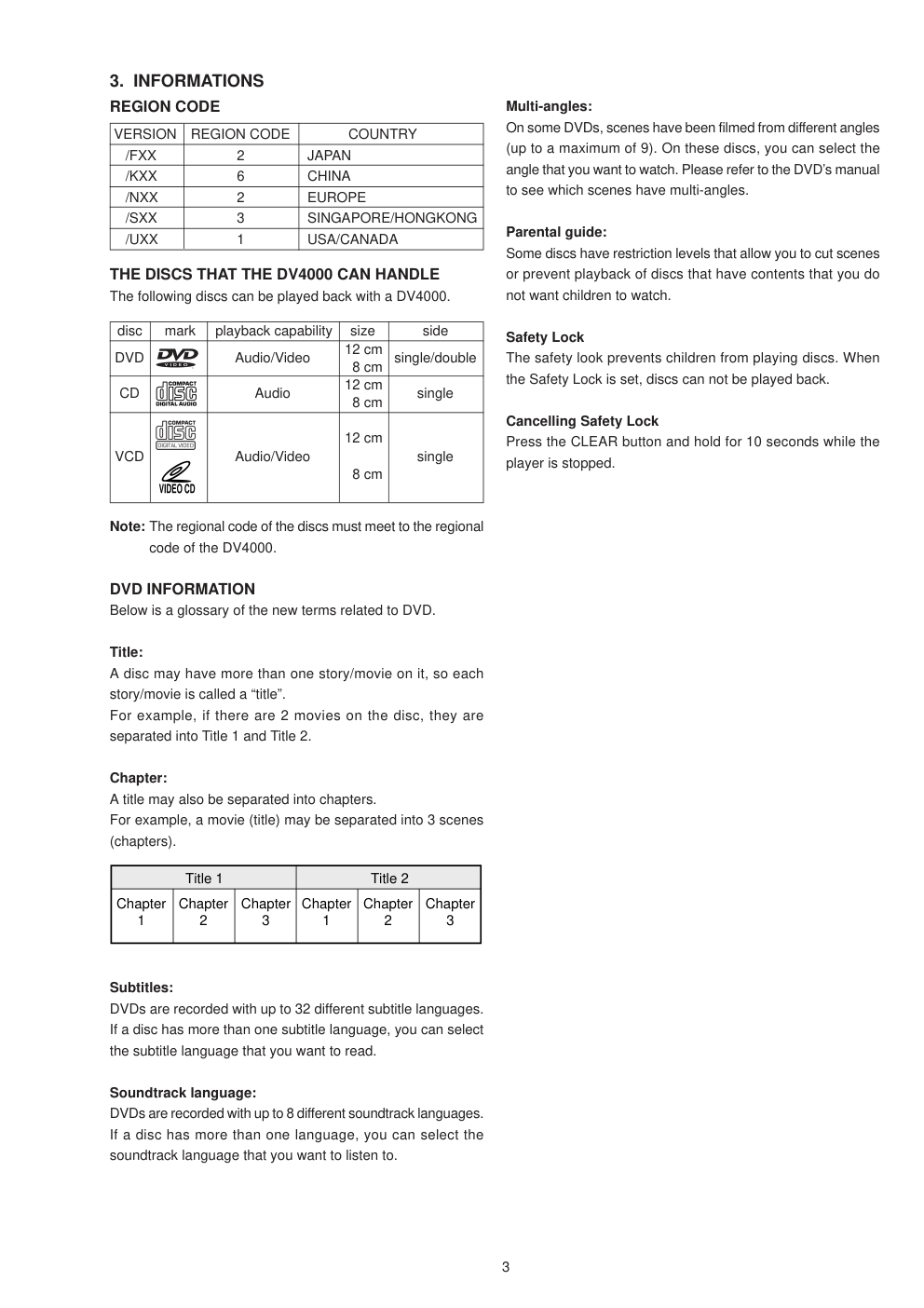
3. INFORMATIONS
REGION CODE
THE DISCS THAT THE DV4000 CAN HANDLE
The following discs can be played back with a DV4000.
Note: The regional code of the discs must meet to the regional
code of the DV4000.
DVD INFORMATION
Below is a glossary of the new terms related to DVD.
Title:
A disc may have more than one story/movie on it, so each
story/movie is called a “title”.
For example, if there are 2 movies on the disc, they are
separated into Title 1 and Title 2.
Chapter:
A title may also be separated into chapters.
For example, a movie (title) may be separated into 3 scenes
(chapters).
Subtitles:
DVDs are recorded with up to 32 different subtitle languages.
If a disc has more than one subtitle language, you can select
the subtitle language that you want to read.
Soundtrack language:
DVDs are recorded with up to 8 different soundtrack languages.
If a disc has more than one language, you can select the
soundtrack language that you want to listen to.
Multi-angles:
On some DVDs, scenes have been filmed from different angles
(up to a maximum of 9). On these discs, you can select the
angle that you want to watch. Please refer to the DVD’s manual
to see which scenes have multi-angles.
Parental guide:
Some discs have restriction levels that allow you to cut scenes
or prevent playback of discs that have contents that you do
not want children to watch.
Safety Lock
The safety look prevents children from playing discs. When
the Safety Lock is set, discs can not be played back.
Cancelling Safety Lock
Press the CLEAR button and hold for 10 seconds while the
player is stopped.
disc
mark
playback capability
size
side
DVD
Audio/Video
12 cm
single/double
8 cm
CD
Audio
12 cm
single
8 cm
12 cm
VCD
Audio/Video
single
8 cm
VERSION
REGION CODE COUNTRY
/FXX
2
JAPAN
/KXX
6
CHINA
/NXX
2
EUROPE
/SXX
3
SINGAPORE/HONGKONG
/UXX
1
USA/CANADA
Title 1
Title 2
Chapter
3
Chapter
1
Chapter
2
Chapter
3
Chapter
1
Chapter
2
SERVICE TOOLS
Audio signals disc
4822 397 30184
Disc without errors (SBC444)+
Disc with DO errors, black spots and fingerprints (SBC444A)
4822 397 30245
Disc (65 min 1kHz) without no pause
4822 397 30155
Max. diameter disc (58.0 mm)
4822 397 60141
Torx screwdrivers
Set (straight)
4822 395 50145
Set (square)
4822 395 50132
13th order filter
4822 395 30204
DVD test disc
4822 397 10131
SERVICE HINTS
4
4. SERVICING HINT
5
5. DISASSEMBLY
In case of trouble, etc., necessitating dismantling, please
dismantle in the order shown in the illustrations. Reassemble
in the reverse order.
1. Removal of the UPPER COVER
2. Removal of the FRONT PANEL
1) Press the “EJECT” button while the unit’s power is turned on and open the DISC TRAY.
2) Remove the decoration plate on the DISC TRAY by pulling it upward.
3) Remove the three retaining screws on the bottom and two screws on each left and right side of the FRONT PANEL as
shown.
4) Disconnect the flat cable from the P702 connector on the OUTPUT PCB .
5) Remove the FRONT PANEL by pulling it forward while releasing the TABs on both left and right ends of the FRONT
PANEL.
TAB
TAB
P702
REMARK : Before disassemble the front panel.
Press open/close button to open the tray.
If the tray doesn’t work, put a small screwdriver into the
hole as shown in picture and slide the knob.
Then the tray comes out. After the first centimeter it is
possible to pull the tray out by hand. Release the door
cover of the tray.
POWER SUPPLY PCB
PICKUP
MAIN PCB
OUTPUT PCB
LOADING MOTOR
SLED MOTOR
SPINDLE MOTOR
OPERATION PCB
6
Fig. 6-1 Top view (DV4000)
6. PRINCIPAL PARTS LOCATION
STOPPER TUB
7-1. Removal of the TRAVERSE MECHA.
7-1-1. Removal of the MECHANISM BLOCK
1) Turn the unit’s power on and press the “EJECT” button to
eject the DISC TRAY.
2) Disconnect the power cord and remove the DISC CLAMPER
BLOCK.
3) Completely remove the DISC TRAY by pulling it outwards
while pulling up both of the stopper tabs alternately.
Fig. 7-1
4) Disconnect the two flat cables from the P803 connectors
and one flat cable from the P808 connector on the MAIN
PCB.
5) Disconnect the P807 connector on the MAIN PCB.
6) Remove the four a retaining screws and remove the
MECHANISM BLOCK from the chassis.
Fig. 7-2
A SCREW
7
7. REPLACEMENT OF PRINCIPAL COMPONENTS
7-1-2. Removal of the TRAVERSE MECHA.
1) Remove the four b screws on the MAIN PCB and then
disconnect the P800 connector on the MAIN PCB.
Fig. 7-3
2) Short the laser diode protection circuit on the PICK UP
BLOCK’s flexible cable with solder as shown.
Caution
To protect the laser diode from damage caused by high voltage
static electricity, a laser diode protection circuit has to be
shorted before disconnecting the flexible cable (P200
connector on the MECHANISM PCB). It is recommended that
you put solder on the top of the soldering iron as shown in Fig.
3-5 then short the circuit at once. When you replace the
TRAVERSE MECHA., be sure to connect the P200 connector
before removing the solder at the shorted parts.
B SCREW
P200
SOLDER
Fig. 7-4
Fig. 7-5
8
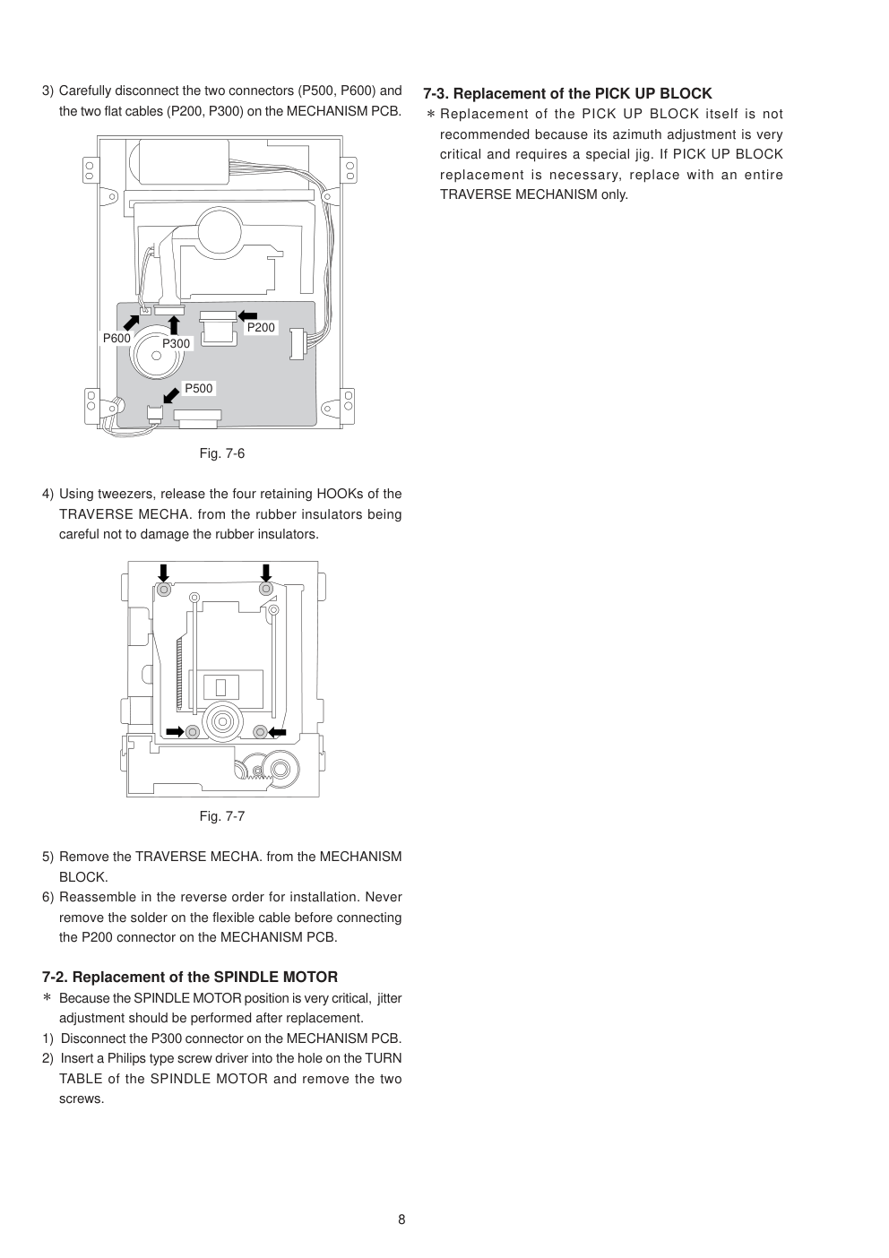
3) Carefully disconnect the two connectors (P500, P600) and
the two flat cables (P200, P300) on the MECHANISM PCB.
Fig. 7-6
4) Using tweezers, release the four retaining HOOKs of the
TRAVERSE MECHA. from the rubber insulators being
careful not to damage the rubber insulators.
Fig. 7-7
5) Remove the TRAVERSE MECHA. from the MECHANISM
BLOCK.
6) Reassemble in the reverse order for installation. Never
remove the solder on the flexible cable before connecting
the P200 connector on the MECHANISM PCB.
7-2. Replacement of the SPINDLE MOTOR
Because the SPINDLE MOTOR position is very critical, jitter
adjustment should be performed after replacement.
1) Disconnect the P300 connector on the MECHANISM PCB.
2) Insert a Philips type screw driver into the hole on the TURN
TABLE of the SPINDLE MOTOR and remove the two
screws.
7-3. Replacement of the PICK UP BLOCK
Replacement of the PICK UP BLOCK itself is not
recommended because its azimuth adjustment is very
critical and requires a special jig. If PICK UP BLOCK
replacement is necessary, replace with an entire
TRAVERSE MECHANISM only.
P200
P300
P600
P500
9
8. SERVICE MODE
8-1.
8-1-1. MAIN
(IC600:MB90574)
NAIN
IC
AV
DEM/ECC
VIDEO
CD-DSP AUDIO-DAC
PRE-AMP
READ-
CHANNEL SERVO
DVD
OSD
DISC
OPE
MAIN
RESET
8-1 OPERATION
8-1-1. Main Microprocessor (IC600 : MB90574)
Functions which operated by main microprocessor
are follows.
Control of following IC's.
AV decoder, DEM/ECC, VIDEO encoder, CD-
DSP, AUDIO-DAC, PRE-AMP, READ-CHANNEL,
SERVO
Mechanism control
DVD rate control
OSD control
DISC detect, Focus/Tracking alignment
Data transmission between OPE microprocessor
Process from POWER ON (RESET RELEASE) till
PLAY BACK are described in the chart below.
Release REST
Initial read EEPROM
EEPROM
Release RESET (IC's)
IC
RESET
VIDEO Encoder initial setup
VIDEO
(PAL or NTSC)
Release RESET (AV Decoder)
AV
RESET
Boot up AV Decoder
AV
BOOT UP
Servo IC initialize
RESET
IC
DEM/ECC initialize
DEM/ECC
Digital out of the AV decoder
initial set up. (48Khz liner PCM)
AV
48KHz
PCM)
Show the start up frame
DISC detect
DISC
CD/VCD
DVD
TOC reading
TOC
Control data
reading
PLAY BACK /
Mechanism initialize
10
8-1-2. OUTPUT CONTROL
(IC700: M38022)
OUTPUT CONTROL
3.3V
ON/OFF
5.0V
ON/OFF
9.0V
ON/OFF
OUTPUT
VIDEO
21PIN SCART
21PIN SCART
(TV/DVD, SQUEEZE, RGB)
S
S1
AUDIO
MUTE
MAIN
OPERATION
FLD
LED
MAIN
FLD/LED
8-1-2. Output Control Microprocessor
(IC700:M38022)
Main operation features of this microprocessor is
as follows.
Power supply control : Power efficiency switching.
3.3V line ON/OFF
5.0V line ON/OFF
9.0V line ON/OFF
Out put selection of the OUTPUT PCB.
VIDEO output stage control
21PIN SCART output signal selection
21PIN SCART control signal selection
(TV/DVD, SQUEEZE, RGB)
AUDIO output control
Output MUTE control
Feedback to the MAIN microprocessor
OPERATION PCB
Operation Button key scan
Remote control code reading
FLD indication
LED indication
Communication between MAIN microprocessor
Command transmission (by user controlable)
Data receiving for FLD/LED indication
S-Video out S1 control
/
In case of no DISC
DVD
/
While DVD Video playback
8-2.
1.
2.
(STOP)
(PAUSE)
FLD
8-2. TEST MODE
How to set up the TEST MODE
1. Remove any Disc from the tray, and turn OFF
the mains power.
2. Turn ON the mains power while depress the " "
(STOP) and " " (PAUSE) buttons together. Do
not release buttons till FLD shows follows.
11
VCD/CD
/
While VCD and CD Video playback
IC600
(CPU :
IC
)
FLD
8-1
In case of some fault has happened. (caused with
communications between CPU: IC600 and related
IC's) Some Error code is shown on the FLD.
Each Error codes are described on the table 8-1.
DISC
CD-DSP(IC490)
D/V/C
D/V/C
D/V/C
D/V/C
V/C
with Servo-DSC (IC300).
D/V/C
D/V/C
D/V/C
D/V/C
D/V/C
D/V/C
D/V/C
D : DVD, V : Video CD, C : CD
8-1. / Table 8-1.
ERORR
CODE
16
17
18
19
20
32
33
34
35
36
37
38
ERORR DESCRIPTION /
No access with CD-DSP (IC490).
Sledge motor is not working.
Tracking ON error.
Focus ON error.
Sub code read error. (CD/VCD)
CD, VCD
No access
DSC(IC300)
with DEM/ECC
DEM/ECC(IC500)
with A/V decoder (IC700).
A/V
(IC700)
No access
(IC500).
No access
No access with system ROM (IC602).
ROM(IC602)
No access with EEPROM(IC603).
EEPROM(IC603)
No access with A/V encoder (IC850).
A/V
(IC850)
No access with Read channel (IC200).
(IC200)
12
3.
(STOP)
FLD
FLD
4.
(STOP)
DVD
DVD
3. Press the "
" (STOP) button while close the
disctray without any disc. Then all segments of
the FLD right ON.
4. Press the "
" (STOP) button again. The FLD
indication shows below. Then the laser diode for
DVD will right ON.
5.
(STOP)
CD
CD
5. Press the " " (STOP) button again. The FLD
indication shows below. Then the laser diode for
CD will right ON.
6.
(STOP)
7.
(Forward Search)
8.
6. Press the "
" (STOP) button again. Then the
TEST MODE back to the first step.
7. Press the "
" (Forward Search) button while
close the disc tray without any disc. Then the
sledge motor will move.
8. Turn OFF the mains power. Then service mode
will be released.
13
U1B
F1N
N1B
S1G
K1G
01
E1
E9
F7
E7
E7
02
30
30
70
30
30
03
00
08
00
00
06
04
53
50
00
00
00
05
55
4A
00
00
00
06
C5
C5
C5
C5
C5
07
A9
A9
A9
A9
A9
Address
Data
8-3. EEPROM initialize
The memory device (EEPROM) which used in this DVD player
is programmed each functions by products regions at factory.
When that EEPROM (MAIN P.C. Board IC602 : M24C16-
MN6T) or MAIN P.C. Board has exchanged, EEPROM initial-
ization is necessary. If that the initialization will not be done
correctly, the product might not be work correctly.
The initialize procedure are as follows.
1. Remove any Disc from the tray, and turn OFF the mains
power.
Turn ON the mains power while depress the “ “ (STOP)
and “ “ (Forward skip) buttons together. Do not release
buttons till FLD shows “ A-01 D-XX “. (XX = is depended
on EEPROM status)
REMARK : In case of some failure with the product. The
ERROR code will be shown on the FLD and above
indication will not be shown. Then other confirmation or
repair is necessary before this EEPROM initialization.
2. The address shown as “ A-01 D-XX “ is can be changed
by pressing “ “ and “ “ buttons on the front panel or
remote controller. Which can be changed to “ 0 “ till “ 07 “.
(Address “ 00 “ is not available.)
“ “ (Forward skip) button
: Address UP
“ “ (Reverse skip) button
: Address DOWN
3. The DATA shown as “ XX “ is can be changed by pressing
“ II “ and “ “ buttons on the front panel or remote
controller. Set up data are shown in following table.
“ II “ (PAUSE) button
: Data UP
“ “ (STOP) button
: Data DOWN
4. Press the “ DIMMER “ button, then address data will be
memorize.
5. Memorize data by each address ( from “ 01 “ to “ 07 “), as
order 2., 3. And 4. processes.
6. Turn OFF the mains switch. (This procedure is necessary
for next procedure.)
14
U1B
F1N
N1B
S1G
K1G
01
02
02
04
20
Data
10. Press the “ ENTER “ button, then address data will be
memorize and the FLD shows a data number which you
stored. ( EX: “ D-02 “ )
11. Turn OFF the mains switch, then EEPROM initialization
mode will be release.
7. Turn ON the mains power while depress the “ DIMMER “
and “ “ (Reverse skip) buttons together. Then the FLD
shows “ -- -- -- -- “.
8. Send the commands “ 1999 “ by the remote controller.
(Press buttons “ 1 “, “ 9 “, “ 9 “ and “ 9 “.) Then the FLD
shows “ A-00 D-XX “. (XX = is depended on EEPROM
status)
9. Send the commands “ D-XX “ (Data) as your product ver-
sion shows in following table by the remote controller.
15
9. ELECTRICAL ADJUSTMENT
9-1. DVD JITTER ADJUSTMENT
1. Stick the provided small round sticker (0.1 mm thickness)
at the innermost position of a DVD disc as shown and make
a swayed DVD disc.
Fig. 9-2
2. Play back the swayed DVD disc and press the F.F button
repeatedly until the pickup block reaches the outermost
position of its movable range. Next, press the PAUSE button.
3. Set the oscilloscope to the DC input mode and connect it to
the TP201 (HOT) and the TP102 (D.GND) on the MAIN
PCB.
4. Adjust the a screw and b screw alternately so that the AC
and DC level of the waveform is minimum. (DC level should
be less than 1.8 V, AC component should be minimum.)
Fig. 9-3
NOTE: If the SPINDLE MOTOR is replaced, this jitter
adjustment should be performed for proper performance.
9-2. SLICE LEVEL ADJUSTMENT
1. Play back an ordinary DVD disc (single side, one layer) and
press the F.F button repeatedly until the pickup block
reaches almost the center position of its movable range.
2. Set the oscilloscope to the DC input mode and connect it to
the TP201 (HOT) and the TP102 (D.GND) on the MAIN
PCB.
3. Adjust the VR202 so that the DC level is minimum. (The DC
level should be less than 1.8 V)
9-3. CD TRACKING BALANCE
1. Set the VR110 at its center position prior to the adjustment.
2. Connect an oscilloscope to the TP150 (TE) on the MAIN
PCB.
3. Play back an ordinary CD-disc and then set it to the PAUSE
mode. If the play mode does not be engage, turn the VR110
at ±15 degrees. If the play mode does still not be engage
even when the VR110 is turned at ±15 degrees, turn the
VR110 at ± 30 degrees and try it again.
4. Observe the waveform and adjust it so that the level A of
the waveform is the same as level B.
Fig. 9-4
Fig. 9-1
TP107
TP105
P800
TP300
VR120
VR121
TP120
VR110
VR202
P807
TP201
P804
P803
JITTER ADJ
SCREW B
JITTER ADJ
SCREW A
Signal recorded side
STICKER
Less than 1.8V
minimum
A
B
500mV
9-4. AS ADJUSTMENT
Adjustment point : VR120
Test point : TP120
1. Turn ON the mains power while depress the “ ” (STOP)
and “ II ” (PAUSE) buttons together. (TEST MODE)
2. Connect the multi meter to test point TP120. Set the multi
meter in DC voltage mode.
3. Press the “ ” (STOP) button several times till the FLD
shows “ LD TEST CD ”. Measure the voltage at that
status.
4. Press the “ ” (STOP) button several times till the FLD
shows “ LD TEST DVD ”.
5. Adjust the voltage at that status 50mV lower than “ LD TEST
CD ” status by the trim resister VR120.
16
17
10. BLOCK DIAGRAM
RF / SERVO / SYSCON
89
CYC11AP000
81
SP_O
SP_N
SP_P
82
80
65
64
62
61 60
58 57
56
52
45
44 46
33
91
90
92
99
100
97 98 95 96 93 94
77 78
73 74
75 76
36 29
34
35
37
41
42
40
69
70
69
71
72
8
7
68
67
66
18
19
AUDIO
Not for DV4000
/N1B ONLY
Not for /N1B
20
21
VIDEO
/N1B ONLY
22
23
11. WIRING DIAGRAM
Not for DV4000
Not For /N1B
/N1B ONLY
Not for /N1B
24
25
OUTPUT-1/2
12. SCHEMATIC DIAGRAM AND PARTS LOCATION
Not for DC4000
26
27
OUTPUT-2-2
28
29
OUTPUT TOP VIEW
OUTPUT BOTTOM VIEW
IC200
TR110
TR200
TR350
TR310
TR320
TR321
TR360
TR361
TR421 TR531 TR530
TR900 TR902 TR901
TR482 TR450
IC719
IC700
IC570
IC470
IC420
IC520
TR400~TR405
TR500~TR505
IC340
TR540~TR542
TR130~TR133
IC250
30
31
OPERATION
Not for DV4000
32
33
OPERATION
PH100
PH120
TR101
TR102
34
35
POWER
36
37
POWER
IC501
PH500
PH501
TR558
TR551
IC551
IC556
IC555
TR550
IC553
TR559
TR560
38
39
13. EXPLODED VIEW AND PARTS LIST
14
010B
003B
002B
006B
005B
001B
020B
011B
013B
019B
012B
018B
001G
POS.
NO
VERS.
COLOR
PART NO.
(FOR PCS)
DESCRIPTION
PART NO.
(MJI)
(VERS. :VERSION, U:U.S.A., F:JAPAN, K:FAR EAST, **:EUROPE)
POS.
NO
VERS.
COLOR
PART NO.
(FOR PCS)
DESCRIPTION
PART NO.
(MJI)
001B
/F1N,/S1
G,/K1G
PANEL FRONT (GLD)HB
294W248110
001B
/U1B
PANEL FRONT (BLK)V2
294W248020
001B
/N1B
9965 000 04731
PANEL FRONT (BLK)HB
294W248010
002B
9965 000 04735
WINDOW FLD
294W158010
003B
4822 454 11825
BADGE MARANTZ
185J251010
005B
/F1N,/S1
G,/K1G
PANEL TRAY (GLD)
294W053110
005B
/U1B
/N1B
9965 000 04745
PANEL TRAY (BLK)
294W053010
006B
/F1N,/S1
G,/K1G
PLATE DVD (GLD)
294W251110
006B
/U1B
/N1B
9965 000 04736
PLATE DVD (BLK)
294W251010
010B
/F1N,/S1
G,/K1G
BUTTON POWER (GLD)
294W270110
010B
/U1B
/N1B
9965 000 04743
BUTTON POWER (BLK)
294W270010
011B
/F1N,/S1
G,/K1G
BUTTON PLAY (GLD)
294W270120
011B
/U1B
/N1B
9965 000 04732
BUTTON PLAY (BLK)
294W270020
012B
/F1N,/S1
G,/K1G
BUTTON SURROUND (GLD)
294W270130
012B
/U1B
/N1B
9965 000 04733
BUTTON SURROUND (BLK)
294W270030
013B
/F1N,/S1
G,/K1G
BUTTON EJECT (GLD)
294W270140
013B
/U1B
/N1B
9965 000 04734
BUTTON EJECT (BLK)
294W270040
018B
9965 000 04737
LENS POWER
294W355010
019B
9965 000 04738
LENS DTS
294W355020
020B
9965 000 04739
LENS WIDE
294W355030
001G
9965 000 04744
JOINT POWER
294W357010
12
nsp
BT BID26X08STL CMT
nsp
13
9965 000 04740
FFC BD P1.0 L230 14P
*YU000590R
14
nsp
ST BID30X06STL CMT
nsp
15
nsp
BT BID30X14STL NI3
nsp
16
9965 000 04741
FFC BD P0.5 L160 24P
*YU000620R
17
/F1N
nsp
PANEL REAR DV4000 (J) (CH)
nsp
17
/U1B
nsp
PANEL REAR DV4000(A) (CH)
nsp
17
/N1B
nsp
PANEL REAR DV4000 (E) (CH)
nsp
17
/S1G
nsp
PANEL
REAR
DV4000(U5)
(CH)
nsp
17
/K1G
nsp
PANEL
REAR
DV4000(Y4)
(CH)
nsp
18
nsp
BT BID30X08STL BZN
nsp
20
9965 000 04742
FOOT
294W057010
21
nsp
CUSHION FOOT 12X12X2 (CH)
nsp
22
nsp
ST BID30X10STL CMT
Nsp
25
/F1N,/S1
G,/K1G
nsp
COVER UPPER (G) (CH)
nsp
25
/U1B
/N1B
nsp
COVER UPPER (B) (CH)
nsp
26
nsp
BT BID30X08STL BZN
nsp
27
/F1N,/S1
G,/K1G
nsp
ST BID40X06STL COP CLEAR
nsp
27
/U1B
/N1B
nsp
ST BID40X06STL BZN
Nsp
PACKING
001T
/F1N
USER GUIDE (JPN)
294W851110
001T
/K1G
USER GUIDE (ENG/CHINA)
294W851350
001T
/N1B
9965 000 04748
9965
*YC000420R
*YC000430R
*YC000410R
*YC000440R
MAINS CORD (JPN)
MAINS CORD (USA)
MAINS CORD (EUR/S-pore)
MAINS CORD (CHINA)
000 04747
USER GUIDE (5LANGUAGE)
294W851310
001T
/S1G
USER GUIDE (ENG/CHINA)
294W851350
001T
/U1B
/F1N
/U1B
/N1B
/S1G
/K1G
USER GUIDE (ENG/FRAN)
294W851250
001Z
9965 000 04746
REMOTE CONTROLLER
RC4000DV
ZK294W0010
002Z
/N1B
nsp
CORD 21P YAF11-0642 1.5M
nsp
ASSIGNMENT OF COMMON PARTS CODES.
RESISTORS
R
1) GD05 x x x 140, Carbon film fixed resistor, 5% 1/4W
R
2) GD05 x x x 160, Carbon film fixed resistor, 5% 1/6W
1 Resistance value
Examples
1 Resistance value
0.1
..... 001
10
......100
1k
......102
100k
...... 104
0.5
..... 005
18
......180
2.7k
......272
680k
...... 684
1
..... 010
100
......101
10k
......103
1M
...... 105
6.8
..... 068
390
......391
22k
......223
4.7M
...... 475
Note : Please distinguish 1/4W from 1/6W by the shape of parts
used actually.
CAPACITORS
C : CERAMIC CAP.
3) DD1 x x x x 370, Ceramic capacitor
Disc type
Temp.coeff. P350~N1000, 50V
3 Capacity value
2 Tolerance
Examples
2 Tolerance (Capacity deviation)
0.25 pF ....... 0
0.5 pF ....... 1
5 % ....... 5
Tolerance of COMMON PARTS handled here are as follows :
0.5 pF - 5 pF .......
0.25 pF
6 pF - 10 pF .....
0.5 pF
12 pF - 560 pF ...
5 %
3 Capacity value
0.5 pF .... 005
3 pF ..... 030
100 pF ..... 101
1 pF .... 010
10 pF ..... 100
220 pF ..... 221
1.5 pF .... 015
47 pF ..... 470
560 pF ..... 561
C : CERAMIC CAP.
4) DK16 x x x 300, High dielectric constant ceramic
capacitor
Disc type
Temp.chara. 2B4, 50V
4 Capacity value
Examples
4 Capacity value
100 pF .....101
1000 pF .... 102
10000 pF .... 103
470 pF .....471
2200 pF .... 222
C
: 5) ELECTROLY CAP.( ), 6)FILM CAP ( )
5) EA x x x x x x 10, Electrolytic capacitor
One-way lead type,Tolerance 20%
6 Working voltage
5 Capacity value
Examples
5 Capacity value
0.1
F .... 104
4.7
F .... 475
100
F ..... 107
0.33
F .... 334
10
F .... 106
330
F ..... 337
1
F .... 105
22
F .... 226
1100
F ..... 118
2200
F .... 228
6 Working voltage
6.3 V ...... 006
25 V ..... 025
10 V ...... 010
35 V ..... 035
16 V ...... 016
50 V ..... 050
6) DF15 x x x 350
Plastic film capacitor
DF15 x x x 310
One-way type, Mylar 5% 50V
DF16 x x x 310
Plastic film capacitor
One-way type, Mylar 10% 50V
7 Capacity value
Examples
7 Capacity value
0.001
F (1000 pF) ...... 102
0.1 F......104
0.0018
F........................ 182
0.56 F......564
0.01
F........................ 103
1 F......105
0.015
F........................ 153
1) The above CODES(R
,R
,C
,C
and C
) are omitted on the schematic diagram in
some case.
2) On the occasion, be confirmed the common parts on the
parts list.
3) Refer to “Common Parts List” for the other common
parts(Rl05, DD4, DK4).
NOTE
NOTE ON SAFETY:
Symbol Fire or electrical shock hazard. Only original
parts should be used to replaced any part marked with
symbol Any other component substitution ( other than
original type), may increase risk of fire or electrical shock
hazard.
990521 A.O
NOTE ON SAFETY FOR FUSIBLE RESIST OR :
The suppliers and their type numbers of fusible resistors are as
follows ;
1 . KOA Corporation
Part No.(MJI)
Type No.(KOA)
Description
NH05 x x x 140
RF25S x x x x
J
J
J
J
5% (1/4W)
NH05 x x x 120
RF50S x x x x
5% (1/2W)
NH85 x x x 110
RF73B2A x x x x
5% (1/10W)
NH95 x x x 140
RF73B2E x x x x
5% (1/4W)
Resistance value Resistance value(0.1
- 10k
)
2. Matsushita Electronic Components Co., Ltd
Part No.(MJI)
Type No.(MEC)
Description
NF05 x x x 140
ERD-2FCJ x x x
( 5% 1/4W)
RF05 x x x 140
NF02 x x x 140
ERD-2FCG x x x
( 2% 1/4W)
RF02 x x x 140
Resistance value
Examples
Resistance value
0.1
..... 001
10
..... 100
1k
..... 102
100k
..... 104
0.5
..... 005
18
..... 180
2.7k
..... 272
680k
..... 684
1
..... 010
100
..... 101
10k
..... 103
1M
..... 105
6.8
..... 068
390
..... 391
22k
..... 223
4.7M
..... 475
ABBREVIATION AND MARKS
ANT.
: ANTENNA
BATT.
: BATTERY
CAP.
: CAPACITOR
CER.
: CERAMIC
CONN.
: CONNECTING
DIG.
: DIGITAL
HP
: HEADPHONE
MIC.
: MICROPHONE
-PRO
: MICROPROCESSOR
REC.
: RECORDING
RES.
: RESISTOR
SPK
: SPEAKER
SW
: SWITCH
TRANSF.
: TRANSFORMER
TRIM.
: TRIMMING
TRS.
: TRANSISTOR
VAR.
: VARIABLE
X’ TAL
: CRYSTAL
:
:
40
14. ELECTRICAL PARTS LIST
41
POS.
NO
VERS.
COLOR
PART NO.
(FOR PCS)
DESCRIPTION
PART NO.
(MJI)
(VERS. :VERSION, U:U.S.A., F:JAPAN, K:FAR EAST, **:EUROPE)
POS.
NO
VERS.
COLOR
PART NO.
(FOR PCS)
DESCRIPTION
PART NO.
(MJI)
OPERATION CIRCUIT BOARD
DIODES
D101
9965 000 04668
1SS133T-77 T26
*HD201380R
D102
9965 000 04668
1SS133T-77 T26
*HD201380R
D105
9965 000 01138
MTZJ4.7C T26
*HD301820R
D106
4822 130 82609
MTZJ2.0B T26
*HD301780R
D120
9965 000 04669
LED SEL5421ETP15
*HI100850R
D121
9965 000 04669
LED SEL5421ETP15
*HI100850R
D122
9965 000 04669
LED SEL5421ETP15
*HI100850R
D123
9965 000 04670
LED SEL2910ATP6 ORANGE
HI10031080
D124
9965 000 04670
LED SEL2910ATP6 ORANGE
HI10031080
D140
9965 000 04671
LED SPR325MVWT31
*HI100840R
D142
9965 000 04672
MTZJ2.0A T26
*HD301760R
INTEGRATED CIRCUITS
IC100
4822 209 90244
IC UPD16311GC-AB6
HC10283060
TRANSISTORS
PH120
9965 000 04674
IR SPS-440-4-E
*HW100460R
TR101
4822 130 61892
2SD2144S U/V/W
*HT400420R
TR102
4822 130 60889
DTA143ES
*BA000800R
MISCELLANEOUS
FL100
9965 000 04673
FLD 13-BT-160GK
*HQ300410R
P102
nsp
SOCKET 14-FMZ-ST 14P
nsp
SW101
4822 276 20508
SW TACT SKHVBE
SP0101128X
SW102
4822 276 20508
SW TACT SKHVBE
SP0101128X
SW103
4822 276 20508
SW TACT SKHVBE
SP0101128X
SW104
4822 276 20508
SW TACT SKHVBE
SP0101128X
SW105
4822 276 20508
SW TACT SKHVBE
SP0101128X
SW106
4822 276 20508
SW TACT SKHVBE
SP0101128X
SW120
4822 276 20508
SW TACT SKHVBE
SP0101128X
SW121
4822 276 20508
SW TACT SKHVBE
SP0101128X
POWER CIRCUIT BOARD
CAPACITORS
C509
nsp
CER.
1000pF 400V
nsp
C511
nsp
CER.
1000pF 400V
nsp
C512
nsp
CER.
1000pF 400V
nsp
C513
nsp
MYLAR
0.1 F 275V
nsp
C514
nsp
MYLAR
0.22 F 275V
nsp
DIODES
D502
9965 000 04668
1SS133T-77 T26
*HD201380R
D504
9965 000 04668
1SS133T-77 T26
*HD201380R
D508
9965 000 04675
1N4006N02 800/1A
*HD201300R
D509
9965 000 04675
1N4006N02 800/1A
*HD201300R
D510
9965 000 04675
1N4006N02 800/1A
*HD201300R
D511
9965 000 04675
1N4006N02 800/1A
*HD201300R
D553
9965 000 04676
AK03V0 T26
*HD201310R
D555
9965 000 04677
1SS244T-77T26 250/0.2A
*HD201370R
D556
5322 130 10293
FMB-G14L 40/5.0A
*HD201340R
D557
9965 000 04678
RK16LF-C1 S15 60/1.5A
*HD201350R
D558
9965 000 04679
AK06V0 T26 60/0.7A
*HD201360R
D559
9965 000 04679
AK06V0 T26 60/0.7A
*HD201360R
D564
4822 130 11643
MTZJ5.1C T26
*HD301770R
INTEGRATED CIRCUITS
IC501
9965 000 04685
IC STR-F6672
*HC105280R
IC551
9965 000 04686
IC KA431AZTA
*HC105270R
IC553
9965 000 04687
IC KA278R33
*HC105260R
IC555
9965 000 04692
IC NJM79M09FA
HC3950909F
IC556
4822 209 33232
IC NJM78M09FA
HC3850909F
TRANSISTORS
TR550
9965 000 04706
DTC143ZS
*BA000810R
TR551
9965 000 04707
2SB1326 Q/R
*HT200380R
TR558
9965 000 04706
DTC143ZS
*BA000810R
TR559
9965 000 04706
DTC143ZS
*BA000810R
TR560
9965 000 04707
2SB1326 Q/R
*HT200380R
RESISTORS
FR551
9965 000 04680
0.24
10% 1/4W FUSE
*NH000110R
FR552
9965 000 04680
0.24
10% 1/4W FUSE
*NH000110R
FR554
9965 000 04681
0.1
10% 1/4W FUSE
NH05001140
FR555
9965 000 04682
0.75
10% 1/4W FUSE
*NH000130R
FR556
9965 000 04683
22
5% 1/4W FUSE
*NH000120R
R504
4822 050 26801
680
5% 1/4W
GG05681140
R505
9965 000 04701
0.36
5% 1W
*GA000180R
R508
9965 000 04702
5.6
5% 1/4W
GG05056140
R512
9965 000 04703
68K
5% 1W
GA05683010
R553
9965 000 04704
0.75
5% 2W
*GA000170R
MISCELLANEOUS
F500
9965 000 04684
FUSE 219 T 250V 3.15A
*FS000720R
L500
9965 000 04693
COIL LF-4ZA-E263 26.0mH
*LC200120R
L501
9965 000 04694
COIL LU-8SA-V102 1.0mH
*LC200130R
L551
9965 000 04695
COIL FIX 2 PC7 330K
*LC107270R
L553
9965 000 04696
COIL FIX 1 EL0606RA 330J
LC13333000
L554
9965 000 04696
COIL FIX 1 EL0606RA 330J
LC13333000
L556
9965 000 04695
COIL FIX 2 PC7 330K
*LC107270R
L557
9965 000 04697
COIL FIX 1 EL0606RA 101J
LC11043000
PH500
9965 000 04698
PHOTO COUP. PF5001-B
*HC200080R
PH501
9965 000 04699
PHOTO COUP. PS2561-1-V
*HC200070R
P500A /F1N,/K1
G,/N1B
/S1G
9965 000 04700
MAINS INLET M1932 1P
*YT001950R
P500B /U1B
MAINS INLET M1934 1P
*YT001960R
SW500
9965 000 04705
SW PUSH SDKLA10200 01-1
*SP000990R
T501
9965 000 04708
TRANS MAINS D6003KALL
*TS001150R
OUTPUT CIRCUIT BOARD
DIODES
D110
9965 000 04620
1SS355TE-17
*HD201320R
D111
9965 000 04620
1SS355TE-17
*HD201320R
D112
9965 000 04620
1SS355TE-17
*HD201320R
D120
9965 000 04620
1SS355TE-17
*HD201320R
D121
9965 000 04620
1SS355TE-17
*HD201320R
D350
9965 000 04620
1SS355TE-17
*HD201320R
D351
9965 000 04620
1SS355TE-17
*HD201320R
D540
/N1B
9965 000 04709
UDZ6.2BTE-17
*HD301790R
D541
/N1B
9965 000 04710
UDZ12BTE-17
*HD301800R
D900
9965 000 04620
1SS355TE-17
*HD201320R
INTEGRATED CIRCUITS
IC200
9965 000 04711
IC TC7SET08FTE85L
*HC105290R
IC250
9965 000 04713
IC TC74HCU04AF
*HC105310R
IC340
9965 000 04714
IC NJM4580M
*HC105240R
IC470
9965 000 04715
IC BA7666FS-E2
*HC105460R
IC520 /N1B
4822 209 83368
IC TC4053BF
HC405300Z0
IC570 /N1B
9965 000 04716
IC BA7660FS-E2
*HC105250R
IC700
9965 000 04717
IC M38034M4-053FP
*HC105510R
IC719
9965 000 04718
IC XC61AN4002MR
*HC105410R
TRANSISTORS
TR110
4822 130 10982
2SA1037AK R/S
*HT100470R
TR130
9965 000 04707
2SB1326 Q/R
*HT200380R
TR131
9965 000 04725
2SD2097 Q/R/S
*HT400430R
TR132
9965 000 04726
DTC143ZKA
*BA000840R
TR133
9965 000 04727
DTA143ZKA
*BA000830R
TR200
9965 000 04727
DTA143ZKA
*BA000830R
TR350
9965 000 04727
DTA143ZKA
*BA000830R
TR360
9965 000 04728
2SD2114K
HX421141V0
TR361
9965 000 04728
2SD2114K
HX421141V0
TR400
4822 130 10982
2SA1037AK R/S
*HT100470R
TR401
4822 130 10982
2SA1037AK R/S
*HT100470R
TR402
4822 130 10982
2SA1037AK R/S
*HT100470R
TR403
9965 000 04729
2SC2412K R/S
*HT300710R
42
POS.
NO
VERS.
COLOR
PART NO.
(FOR PCS)
DESCRIPTION
PART NO.
(MJI)
(VERS. :VERSION, U:U.S.A., F:JAPAN, K:FAR EAST, **:EUROPE)
TR404
9965 000 04729
2SC2412K R/S
*HT300710R
TR405
9965 000 04729
2SC2412K R/S
*HT300710R
TR420
9965 000 04729
2SC2412K R/S
*HT300710R
TR421
9965 000 04729
2SC2412K R/S
*HT300710R
TR450
9965 000 04726
DTC143ZKA
*BA000840R
TR482
9965 000 04729
2SC2412K R/S
*HT300710R
TR500 /N1B
4822 130 10982
2SA1037AK R/S
*HT100470R
TR501 /N1B
4822 130 10982
2SA1037AK R/S
*HT100470R
TR502 /N1B
4822 130 10982
2SA1037AK R/S
*HT100470R
TR503 /N1B
9965 000 04729
2SC2412K R/S
*HT300710R
TR504 /N1B
9965 000 04729
2SC2412K R/S
*HT300710R
TR505 /N1B
9965 000 04729
2SC2412K R/S
*HT300710R
TR530 /N1B
9965 000 04726
DTC143ZKA
*BA000840R
TR531 /N1B
9965 000 04729
2SC2412K R/S
*HT300710R
TR540 /N1B
4822 130 10982
2SA1037AK R/S
*HT100470R
TR541 /N1B
9965 000 04726
DTC143ZKA
*BA000840R
TR542 /N1B
9965 000 04726
DTC143ZKA
*BA000840R
TR580 /N1B
9965 000 04729
2SC2412K R/S
*HT300710R
TR581 /N1B
9965 000 04729
2SC2412K R/S
*HT300710R
TR582 /N1B
9965 000 04729
2SC2412K R/S
*HT300710R
TR900
4822 130 10982
2SA1037AK R/S
*HT100470R
TR901
9965 000 04729
2SC2412K R/S
*HT300710R
TR902
9965 000 04729
2SC2412K R/S
*HT300710R
MISCELLANEOUS
J200
4822 267 31369
SOCKET OPTICAL GP1F32T
YJ15000090
J500
/N1B
9965 000 04719
SCART YKF41-5021 21P
*YT001970R
L250
9965 000 04720
TRANS PULSE TC-1027-04
*TP000030R
PJ250
9965 000 04721
RCA JACK HSP-241V1B (1P)
*YT002000R
PJ300 /F1N,/K1
G,/S1G
/U1B
RCA JACK HSP-243V2-07 (3P)
*YT001980R
PJ400
9965 000 04722
S-VIDEO HDC-050A (4P)
*YT001990R
PJ900
9965 000 04723
RCA JACK HSP-242V3-23 (2P)
*YT002010R
SW900
9965 000 04724
SW SLIDE SK12P7.2G4 1-01-02 *SS000610R
X722
9965 000 04730
RESONATOR CCR8.0MC5T
*FQ000420R
<
版权声明
1. 本站所有素材,仅限学习交流,仅展示部分内容,如需查看完整内容,请下载原文件。
2. 会员在本站下载的所有素材,只拥有使用权,著作权归原作者所有。
3. 所有素材,未经合法授权,请勿用于商业用途,会员不得以任何形式发布、传播、复制、转售该素材,否则一律封号处理。
4. 如果素材损害你的权益请联系客服QQ:77594475 处理。