马兰士MARANTZ 2250B音响服务手册
 "马兰士MARANTZ 2250B音响服务手册-0")
 "马兰士MARANTZ 2250B音响服务手册-1")
 "马兰士MARANTZ 2250B音响服务手册-2")
 "马兰士MARANTZ 2250B音响服务手册-3")
 "马兰士MARANTZ 2250B音响服务手册-4")
 "马兰士MARANTZ 2250B音响服务手册-5")
 "马兰士MARANTZ 2250B音响服务手册-6")
 "马兰士MARANTZ 2250B音响服务手册-7")
 "马兰士MARANTZ 2250B音响服务手册-8")
 "马兰士MARANTZ 2250B音响服务手册-9")
3.
AM ALIGNMENT
PROCEDURE
(~
3.1
AM
IF Alignment
(
)
1. Connect a sweep generator to the J 153 and an alignment scope to the test point B.
2. Rotate each core of I F transformer
L153 for
maximum height and flat top symmetrical
response.
3.2
AM
Frequency Rangeand Tracking Alignment
1. Set AM signal generator to 515 kHz. Turn the tuning capacitor fully closed (place the tuning
pointer
at the low end) and adjust the oscillator
coil
L152 for maximum audio output.
2. Set the signal generator to 1650 kHz. Placethe tuning pointer in the high frequency end and
adjust the oscillator trimmer on the oscillator
tuning capacitor for maximum audio output.
3.
Repeat steps 1 and 2 until no further adjustment is necessary.
4. Set the generator to 600 kHz and tune the receiver to the same frequency anq adjust a slug
core of AM ferrite rod antenna and RF coil L151 for maximum output.
5. Set the generator to 1400 kHz and tune the receiver to the samefrequency and adjust both
trimming
capacitors of antenna and RF tuned circuit for maximum output.
6. Repeat steps 4 and 5 until no further adjustment is necessary.
Note:
During tracking alignment reduce the signal generator output
as necessaryto avoid AGC
action.
3.3
AM Signal Strength Meter Alignment
Set an AM
signal generator to
1000 kHz at 5k1-N, and adjust R178 so that the signal
strength meter may read 90% of the full scale.
,
1
3
4.
FM ALIGNMENT
PROCEDURE
1. ,Connect an FM signal generator to the FM ANTENNA
terminals and an oscilloscope and an
audio distortion
analyzer to the TAPE OUTPUT jacks on the rear panel.
2. Set the FM SG to 87 MHz and provide about 3 to 5J.1.V.Placethe tuning pointer at the low
frequency
end by rotating the tuning knob and adjust the core of oscillator coil L104 to
obtain maximum audio output.
3. Set the FM SG to 109 MHz and provide about 3 to 5J.1.Voutput.
Rotate the tuning knob and
place the tuning pointer at the high frequency end and adjust the trimming capacitor C106
for maximum output.
4.
Repeat steps 2 and 3 until no further adjustment is necessary.
5. Set the FM SG to 90 MHz and tune the receiver to the same frequency. Decreasesignal
generator
output
until
the audio output
level decreases with
the decreasing generator
output.
Adjust the antenna coil L101, RF coils L102 and L103 and I F transformer L 105 for
minimum audio distortion.
6. Set the FM SG to 106 MHz and tune the receiver to the same frequency. Adjust the trim-
ming capacitor C102, C104 and C105 for minimum distortion.
7. Repeat steps 5 and 6 until no further adjustment is necessary.
8. Adjust the secondary core (upper) of discriminator
transformer
L201 so that the center tun-
ing meter pointer
indicates its center at no signal applied. Set the FM SG to 98 MHz and
increase its output level I kJ.l.Vand tune the receiver to the samefrequency so that the center
tuning meter pointer indicates its center.
Adjust the primary core (lower) of L201 for minimum distortion.
9. Set the FM SG to 98 MHz at 1000 kJ.l.V,and adjust R374 so that the signal strength meter
may read 90% ofthe
full scale.
5.
STEREO SEPARATION
ALIGNMENT
1. Set the FM SG to provide I kj.LVat 98 MHz. Tune the receiver to the samefrequency so that
the center tuning meter pointer indicates its center.
2. Turn the FM SG modulation
off
(with
the pilot
signal turned off), connect a frequency
counter to test point J310, and adjust R311 so that the frequency counter may precisely
read 19 kHz.
3. Modulate the FM SG with stereo composite signal consisting only of subchannel signal (of
course a pilot signal must be included).
4. Adjust the trimming
resistor R301 for maximum
and same separation in both channels.
6.
MUTING
CIRCUIT
ALIGNMENT
1. Connect a VTVM
across the resistor R363 and adjust the resistor R363 until
the meter
reads 0.75V DC at no signal.
2. Set the FM SG to provide I kJ1Vat 98 MHz and tune the receiver to the same frequency
correctly.
3. Turn on MUTI NG push switch. Shift the FM signal generator frequency to plus and minus
and note both plus and minus shifted frequencies at which undesirable audio side responses
are muted out. Adjust the R363 so that the same shifted frequencies mute the undesirable
side response.
4. Adjust R362 for proper frequency shift at which the muting circuit operates.
7.
DOLBY
FM TAPE OUTPUT SETTING
1. Set the modulation of FM SG to 400 Hz, 50% (±37.5 kHz Dev.)
2. Set the FM SG to provide 1 kJ1V at 98 MHz. Tune the receiver to the same frequency so
that the center tuning meter pointer indicates its center.
3. Turn on DOLBY FM push switch. Set the semifixed resistors RC01 and RC02 so that the
output of the TAPE OUTPUT terminals Rand L become 580 mVat VTVM.
8.
AUDIO
ADJUSTMENT
1. Voltage adjustment
Connect a DC voltmeter
between pin terminal
804 and 805, and adjust the trimming
resistor R806 for 35V DC.
2. Main Amplifier
DC off--set alignment
Connect a DC voltmeter with 0.5 or 1 V range between the speakerterminals and adjust the
trimming
resistor R707 for "zero"
DC output on the meter.
Repeat the same procedure for the other channel.
Note:
During this alignment no load should be connected to the speakerterminals.
3. Idle-current adjustment
Connect a VTVM
between pin terminals 708 and 710. Next, adjust the trimming
resistor
R719 so the VTVM reads10mV DC. Repeat the sameprocedure for the other channel.
4. Check DC off-set voltage aligned in the procedure 2 and if any DC output is observed on the
DC voltmeter, adjust the R707 again for "zero" output.
5. Phono-amplifier adjustment
Connect an oscilloscope to the TAPE
OUT jacks and an audio signal generator to the
PHONO jacks. Placethe selector switch in the PHONO position. Increase1 kHz audio signal
gradually until
a slight clipping on top of the sine-wave is observed on the oscilloscope.
Adjust the trimming
resistor R408 for equal clipping level.
For the other channel adjust R409.
4
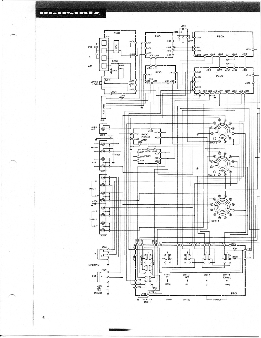
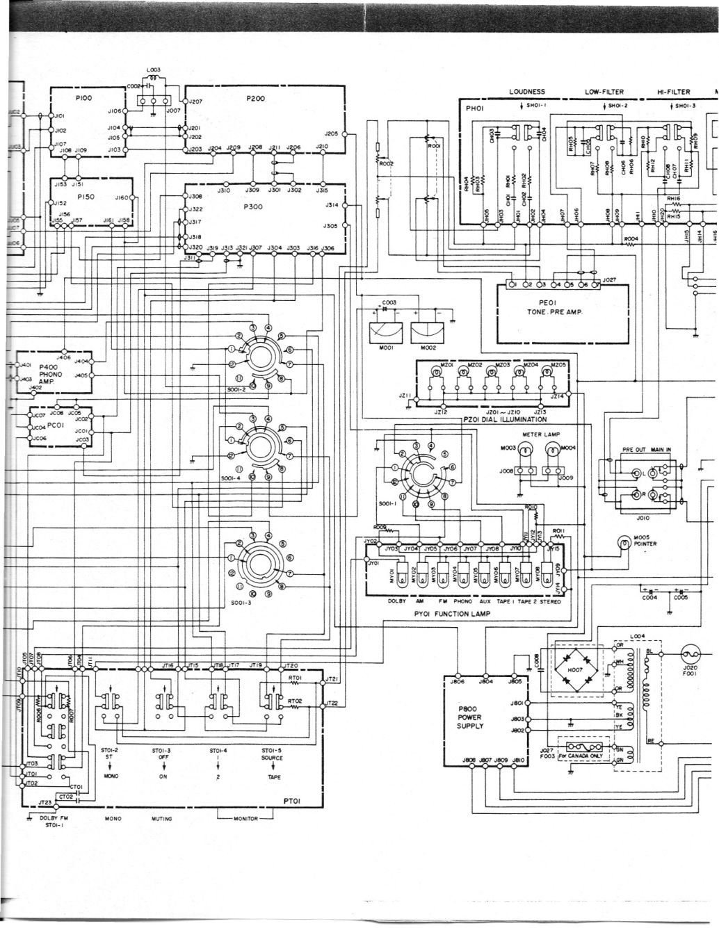
:
Figure 1. Dial Stringing
5
COO3
-
J314
<
J305
<
II
J304
.1303
J316 306
J205 (:r-
J:OS
J "JSP6
J210
:...-....J
--,--
J:;02 -~h
P200
J309
P300
J310
J~
J~9
T I
J317
J318
J320
J319 J1'3
J321 J307
J31lI.
TP
r
I
r---
t-----<
J308
J322
I
i
JI60
JI"
J158:
--
I
,.-J
I
I
JU04
1
.--
G
I
PUOI ---.
r--
IJUOI
I
I
PIOO
0-1--""-
JU02
01
FM
{
0-1- § ~
[~JI02
!.
~ l
~JIC1
7L 0-
JUQ3
-r'
;108
~09
D-
0008
O~
1I
-r
CU02n
I
JI"
J!~'!50
,.J
).J1S2
JI56
IRU04
J~
)-
IJ\5.5
157
MUTING
t;'"
~
lEVECC-
1
I JU07
I JUO'
cOO2-
AM
>-Z<1_
::;;
-
J~
,
J~
J"
J210
ROO
-
,
~
~
,
,
:--J.
,
:
,
-
•••
,
J309
J301
J302
J31.5
f-I
I
•........• ~
P300
J314
>-
J310
~-v@
~D~
I
@
~
7
,
(j])
'-------"
8
@
®
SOOI~3
Jjp4
J<:Q9
r
J203
J3U
r
J317
J305
I
J318
3061
I
J320
J319 J313 "21
J307
J30.
"03
J316
~H
1
-
--
-
J308
C0CJ2.~r-"1T'- 9JF--
I [0
iJ
J207
J '06 >--
J007
1
JIOO 'l'
ryJ2O'
JI05
J202
LOO3
'-
JI60
JI03--
JI6' J'58:
--
PI50
1 I
JJ02
JlO'
JI53
Jr5r
JI01
;108 JI09
).,'52
r--
I
PIOO
IIItl
I
-
I
I
I
;.....
:...--
n
J
Lc"
II
~U
-
-
--
!~-Ol)r~
~406 J404 >--
I~
7
).,.v.
P400
,j,
~
~~"-'
Pore
PHONO
J405
I
® .£1) ~
AMP_
02
--
I
5001-2
9
~
JC08
JC~02
>-.--
tl
JCOI
---®
@-
JCOJI
~\~
i
,j,
r;z""'
19
<
I
flU
l
I
~
FOOl
--J,.
r--------;!
RE
J027,
,'T1iNd
T
FOO3 t~?N~CN..Y~
lGN
c(
:
,J,
~
.J
J803
J802
JSOl
J804
I
J808
J807 J809
J810i
P900
POWER
SUPPLY
I J8C16
I
T20 __
RTOt
JT2r
I
PTOI
I
[ ~tn
RT02
.JT22
.•.•u
I
Q ?
I
STOI-S
SOURCE
+
TAPE
'T17
JTl9
,~
--
JTI6
ON
.2
STOI-3
STO"O
~F
I
+
+
MUTING
MONO
5101-2
ST
+
..:JNO
:
REMOTE
SPEAKER
JOJ5
....,
SPOKE
J("
r--
--0
L
~-o
1--0
- -0 "
----'-
r
{]
L
{]
rD
JOl3
MOOS
-
J703
J704
J,2.!.8
J714
J705
()~,
.-
J701
J706
L
J708
J702
L.:::.
J71Q
()HOO2
P700
I
MAIN
AMP
J711
J712
r~ J713
JOlT
J709
"-----,..----
J~
--< ).1713
J705()~
-
70J
J706
L .J1'02
J708
P700
~
I
MAIN AMPJ710
-
版权声明
1. 本站所有素材,仅限学习交流,仅展示部分内容,如需查看完整内容,请下载原文件。
2. 会员在本站下载的所有素材,只拥有使用权,著作权归原作者所有。
3. 所有素材,未经合法授权,请勿用于商业用途,会员不得以任何形式发布、传播、复制、转售该素材,否则一律封号处理。
4. 如果素材损害你的权益请联系客服QQ:77594475 处理。